EP2048720A2 - Piezoelectic-actuator driving device and exposure apparatus including the same - Google Patents
Piezoelectic-actuator driving device and exposure apparatus including the same Download PDFInfo
- Publication number
- EP2048720A2 EP2048720A2 EP20080166273 EP08166273A EP2048720A2 EP 2048720 A2 EP2048720 A2 EP 2048720A2 EP 20080166273 EP20080166273 EP 20080166273 EP 08166273 A EP08166273 A EP 08166273A EP 2048720 A2 EP2048720 A2 EP 2048720A2
- Authority
- EP
- European Patent Office
- Prior art keywords
- laminated units
- laminated
- driving device
- piezoelectric actuator
- failure
- Prior art date
- Legal status (The legal status is an assumption and is not a legal conclusion. Google has not performed a legal analysis and makes no representation as to the accuracy of the status listed.)
- Withdrawn
Links
Images


Classifications
-
- G—PHYSICS
- G02—OPTICS
- G02B—OPTICAL ELEMENTS, SYSTEMS OR APPARATUS
- G02B7/00—Mountings, adjusting means, or light-tight connections, for optical elements
- G02B7/02—Mountings, adjusting means, or light-tight connections, for optical elements for lenses
- G02B7/023—Mountings, adjusting means, or light-tight connections, for optical elements for lenses permitting adjustment
-
- G—PHYSICS
- G03—PHOTOGRAPHY; CINEMATOGRAPHY; ANALOGOUS TECHNIQUES USING WAVES OTHER THAN OPTICAL WAVES; ELECTROGRAPHY; HOLOGRAPHY
- G03F—PHOTOMECHANICAL PRODUCTION OF TEXTURED OR PATTERNED SURFACES, e.g. FOR PRINTING, FOR PROCESSING OF SEMICONDUCTOR DEVICES; MATERIALS THEREFOR; ORIGINALS THEREFOR; APPARATUS SPECIALLY ADAPTED THEREFOR
- G03F7/00—Photomechanical, e.g. photolithographic, production of textured or patterned surfaces, e.g. printing surfaces; Materials therefor, e.g. comprising photoresists; Apparatus specially adapted therefor
- G03F7/70—Microphotolithographic exposure; Apparatus therefor
- G03F7/708—Construction of apparatus, e.g. environment aspects, hygiene aspects or materials
- G03F7/70808—Construction details, e.g. housing, load-lock, seals or windows for passing light in or out of apparatus
- G03F7/70825—Mounting of individual elements, e.g. mounts, holders or supports
-
- H—ELECTRICITY
- H02—GENERATION; CONVERSION OR DISTRIBUTION OF ELECTRIC POWER
- H02N—ELECTRIC MACHINES NOT OTHERWISE PROVIDED FOR
- H02N2/00—Electric machines in general using piezoelectric effect, electrostriction or magnetostriction
- H02N2/02—Electric machines in general using piezoelectric effect, electrostriction or magnetostriction producing linear motion, e.g. actuators; Linear positioners ; Linear motors
- H02N2/06—Drive circuits; Control arrangements or methods
-
- H—ELECTRICITY
- H10—SEMICONDUCTOR DEVICES; ELECTRIC SOLID-STATE DEVICES NOT OTHERWISE PROVIDED FOR
- H10N—ELECTRIC SOLID-STATE DEVICES NOT OTHERWISE PROVIDED FOR
- H10N30/00—Piezoelectric or electrostrictive devices
- H10N30/50—Piezoelectric or electrostrictive devices having a stacked or multilayer structure
-
- H—ELECTRICITY
- H10—SEMICONDUCTOR DEVICES; ELECTRIC SOLID-STATE DEVICES NOT OTHERWISE PROVIDED FOR
- H10N—ELECTRIC SOLID-STATE DEVICES NOT OTHERWISE PROVIDED FOR
- H10N30/00—Piezoelectric or electrostrictive devices
- H10N30/80—Constructional details
- H10N30/802—Circuitry or processes for operating piezoelectric or electrostrictive devices not otherwise provided for, e.g. drive circuits
-
- Y—GENERAL TAGGING OF NEW TECHNOLOGICAL DEVELOPMENTS; GENERAL TAGGING OF CROSS-SECTIONAL TECHNOLOGIES SPANNING OVER SEVERAL SECTIONS OF THE IPC; TECHNICAL SUBJECTS COVERED BY FORMER USPC CROSS-REFERENCE ART COLLECTIONS [XRACs] AND DIGESTS
- Y10—TECHNICAL SUBJECTS COVERED BY FORMER USPC
- Y10T—TECHNICAL SUBJECTS COVERED BY FORMER US CLASSIFICATION
- Y10T29/00—Metal working
- Y10T29/42—Piezoelectric device making
Definitions
- the present invention relates to a driving device using a piezoelectric actuator.
- Positioning devices currently used to position optical elements in semiconductor exposure apparatuses are required to have a high positioning accuracy of the order of nanometers. For this reason, piezoelectric actuators are used to drive the positioning devices.
- a laminated piezoelectric actuator has a structure in which thin layers of piezoelectric ceramics and electrode layers are alternately stacked to form several hundreds of layers.
- polarization and voltage application are performed by using a wire connected to an electrode layer serving as an anode and a wire connected to an electrode layer serving as a cathode.
- Japanese Patent Laid-Open No. 2002-257000 discloses that driving can be performed even when failure occurs in wire connection in a fuel injection apparatus including a plurality of piezoelectric actuators. More specifically, a plurality of piezoelectric actuators and a plurality of switches are connected in one-to-one correspondence, and, when failure occurs in wire connection for one of the piezoelectric actuators, the corresponding switch is merely turned off, so that the driving of the remaining piezoelectric actuators is prevented from being affected by the failure.
- Japanese Patent Laid-Open No. 2002-185056 discloses a technique of checking a piezoelectric actuator for failure.
- a reference piezoelectric actuator that normally operates is connected to a target piezoelectric actuator in parallel.
- charges accumulated by charging the reference piezoelectric actuator at a fixed voltage are released to the target piezoelectric actuator.
- the voltage of the reference piezoelectric actuator is detected so as to check whether the target piezoelectric actuator is normal.
- the piezoelectric actuators are used to open and close fuel injectors. Since the piezoelectric actuators are provided corresponding to a plurality of cylinders, even when one of the piezoelectric actuators breaks down, the cylinders corresponding to the other piezoelectric actuators can be used.
- the present invention provides a driving device formed by a laminated piezoelectric actuator which includes a plurality of laminated units arranged in series and in which a short-circuited laminated unit can be separated from a driving circuit.
- the present invention in its first aspect provides a driving device as specified in claims 1 to 5.
- the present invention in its second aspect provides an exposure apparatus as specified in claim 6.
- the present invention in its third aspect provides a device manufacturing method as specified in claim 7.
- Fig. 1 shows a configuration of a laminated piezoelectric actuator according to an embodiment of the present invention in which a plurality of laminated units are arranged in series.
- Fig. 2 is a schematic view of a driving device for driving the laminated piezoelectric actuator shown in Fig. 1 .
- Fig. 3 is a flowchart showing a procedure for detecting a short circuit of a laminated unit in the driving device shown in Fig. 2 .
- Fig. 4 shows a configuration of a lens driving device provided in an exposure apparatus to which the embodiment of the present invention is applied.
- Fig. 5 is a flowchart showing a device manufacturing process using the exposure apparatus.
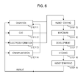
- Fig. 6 is a detailed flowchart showing a wafer process in the flowchart shown in Fig. 5 .
- a piezoelectric actuator serving as a driving device includes a plurality of laminated units.
- the laminated units include a plurality of piezoelectric elements and a plurality of electrode layers, and are arranged in series. Leads serving as an anode and a cathode are connected to each laminated unit. By electrically connecting the laminated units in parallel, voltages can be independently applied to the laminated units.
- a switch is connected to each laminated unit, and is able to provide on/off control.
- a failure detecting unit is provided to detect failure of any of the laminated units. Only a laminated unit whose failure has been detected is separated from a driving circuit by using the switch. This allows the driving device to be used continuously even when one or more laminated units fail.
- a laminated unit whose failure has been detected can be separated from the driving circuit by turning off only the corresponding switch connected to the laminated unit, and this does not affect the operations of the other laminated units which operate normally.
- the same number of switches as the number of laminated units are provided.
- the driving circuit supplies a current for driving to a normal laminated unit (i.e. one for which a failure has not been detected) of a plurality of laminated units, on the basis of the output from the failure detecting unit.
- the failure detecting unit for example, a detection unit for detecting currents passing through a plurality of laminated units or voltages applied to a plurality of laminated units, and a comparison unit for comparing the output of the detection unit with a predetermined reference value can be used. On the basis of the comparison result, the occurrence of failure is detected. For example, when currents are detected, a current much more than in a normal state passes through a piezoelectric actuator that has undergone insulation failure or a short circuit. Hence, insulation failure or a short circuit can be detected by comparing the current passing through the piezoelectric actuator with a normal value (reference value).
- the failure detecting unit for example, a detection unit for detecting displacement of a plurality of laminated units, and a comparison unit for comparing the output of the detection unit with a predetermined reference value can be used. On the basis of the comparison result, the occurrence of failure is detected.
- the driving device is in a normal state, the displacement amount in accordance with the applied voltage is fixed.
- the displacement amount of the piezoelectric actuator in accordance with the applied voltage becomes smaller than in the normal state, or the displacement amount becomes zero. For this reason, when insulation failure or a short circuit occurs, it can be detected by comparing the displacement amount of the piezoelectric actuator with the expected normal value.
- a controller sequentially connects the laminated units one by one by the switches. Then, the failure detecting unit detects insulation failure or a short circuit, and detects a laminated unit in which the insulation failure or short circuit has occurred.
- Fig. 1 shows a configuration of a laminated piezoelectric actuator (driving device) according to a first embodiment of the present invention.
- a piezoelectric actuator 100 according to the first embodiment, multiple thin piezoelectric ceramics plates 2 and multiple electrode layers 3 are alternately stacked and combined.
- the piezoelectric actuator 100 is charged and discharged through leads 4-1, 4-2, 4-3, and 5 connected to the electrode layers 3.
- the piezoelectric actuator 100 is divided into three laminated units 1-1, 1-2, and 1-3.
- the leads 4-1, 4-2, and 4-3 are connected to the electrode layers 3 serving as anodes, and the lead 5 is commonly connected to the electrode layers 3 serving as cathodes.
- the laminated units 1-1, 1-2, and 1-3 can be charged and discharged independently.
- the laminated units 1-1, 1-2, and 1-3 are arranged in series in the expanding and contracting direction thereof. In other words, the amounts of expansion or contraction of the laminated units 1-1, 1-2, and 1-3 are added.
- Fig. 2 shows a driving device including the piezoelectric actuator 100 shown in Fig. 1 and a detection unit for detecting failure of the piezoelectric actuator 100.
- the driving device includes a driving circuit 200, switches 300, a controller 400, a current detection unit 500, and a displacement detection unit 600.
- the driving circuit 200 supplies currents for charging and discharging to the piezoelectric actuator 100 so as to drive the piezoelectric actuator 100.
- the switches 300 are connected to the leads 4-1, 4-2, and 4-3 on the anode sides of the laminated units 1-1, 1-2, and 1-3 in the piezoelectric actuator 100.
- the controller 400 outputs control signals for on/off control of the switches 300.
- the current detection unit 500 detects the current of the piezoelectric actuator 100 from the lead 5 on the cathode side of the piezoelectric actuator 100.
- the displacement detection unit 600 detects the displacement amount of the piezoelectric actuator 100.
- a first failure detecting unit includes the current detection unit 500 and a first comparison unit (comparison circuit) for comparing the detected current with a predetermined first reference value.
- a second failure detecting unit includes the displacement detection unit 600 and a second comparison unit (comparison circuit) for comparing the detected displacement amount with a preset second reference value. These comparison units are provided in a CPU 700.
- the term "failure” mainly refers to a short circuit caused in the piezoelectric actuator by, for example, insulation failure between the electrodes.
- Fig. 3 shows a procedure for detecting failure of the piezoelectric actuator 100.
- the CPU 700 controls the operations of the driving circuit 200, the current detection unit 500, and the displacement detection unit 600.
- Step S1 the CPU 700 compares a detected current value with a preset reference current value, and sends the comparison result to the controller 400.
- the controller 400 determines that there is no failure.
- a case in which the criterion is satisfied means, for example, that the detected current value is less than or equal to the reference current value, or that the detected current value is within a range between two reference current values.
- the controller 400 determines that the piezoelectric actuator 100 is operating normally, the procedure proceeds to Step S2.
- Step S2 all the switches 300 of the laminated units are turned on, and voltage application or discharging is started in Step S3.
- Step S5 is then performed.
- Step S3 the controller 400 applies an arbitrary voltage to the piezoelectric actuator 100 so as to drive an object 800.
- the displacement detection unit 600 detects a displacement amount of the object 800 (or a displacement amount of the piezoelectric actuator 100), and sends the detected value to the CPU 700.
- the CPU 700 compares the detected value with a reference displacement amount of the piezoelectric actuator 100 with respect to the applied voltage, and sends the comparison result to the controller 400.
- the current detection unit 500 for detecting the current of the piezoelectric actuator 100 sends a detected current value to the CPU 700.
- the CPU 700 compares the detected current value with a reference current value, and sends the comparison result to the controller 400.
- Step S5 and subsequent steps it is determined which laminated unit in the piezoelectric actuator 100 is faulty. Steps S5 and subsequent steps will now be described.
- Step S5 detection of a faulty laminated unit is started.
- Step S6 all the switches 300 connected to the laminated units 1-1, 1-2, and 1-3 are turned off.
- Step S7 one of the switches 300 is turned on in Step S7, and a test voltage is applied thereto in Step S8.
- Step S9 a current value and a displacement amount in accordance with the test voltage are detected by the current detection unit 500 and the displacement detection unit 600, and are compared with the reference values so as to determine whether the on-state laminated unit is operating normally.
- Step S11 When it is determined that the laminated unit is operating normally, determination about the laminated unit is completed, Step S11 is performed, and determination about the next laminated unit is performed. In contrast, when it is determined that the laminated unit is short-circuited, the use of the corresponding switch is stopped in Step S10. The faulty laminated unit is thereby separated from the driving circuit 200, and the failure detection is completed in Step S12.
- the driving circuit 200 supplies driving currents to the other laminated units, which are operating normally, on the basis of the output from the failure detecting unit.
- each laminated unit can be electrically separated from the driving circuit, and a faulty laminated unit is separated from the driving circuit.
- the piezoelectric actuator according to the first embodiment has an advantage over the piezoelectric actuator as the related art in its capability to prevent the operation of the driving device from being completely stopped by failure. For example, when it is assumed that the probability that failure will occur between electrodes in one piezoelectric actuator is designated as "a”, the probability that the operation of the piezoelectric actuator as the related art will be completely stopped, in other words, the probability that the piezoelectric actuator as the related art will break down is "a".
- the probability that failure will occurs in each unit is "a/n"
- the probability that the operation of the piezoelectric actuator is completely stopped in other words, the probability that failure occurs in all units is "(a/n) n ". Therefore, reliability becomes higher than in the related art.
- Fig. 4 shows a lens driving device according to a second embodiment of the present invention.
- the lens driving device is preferably used to drive a lens in a projection optical system of an exposure apparatus.
- the lens driving device includes three piezoelectric actuators 8a, 8b, and 8c. This structure allows a lens 7 to be driven in a direction parallel to the optical axis AX or to be inclined with respect to the optical axis AX.
- each piezoelectric actuator two laminated units are arranged in series. Switches 300 are connected to the corresponding laminated units, and on/off control can be exerted on the switches 300 according to a control signal from a controller 400.
- the piezoelectric actuators 8a, 8b, and 8c are connected to a current detection unit 500 for detecting current values of the piezoelectric actuators, and the detected current values are sent to a CPU 700.
- a displacement detection unit 600 includes three displacement sensors 9a, 9b, and 9c, and can detect displacement amounts of the piezoelectric actuators. The detected displacement amounts are sent to the CPU 700.
- the CPU 700 receives signals from the current detection unit 500 and the displacement detection unit 600, enables or disables the current supply to the laminated units in the piezoelectric actuators according to the procedure shown in Fig. 3 , and then sends a selection signal to the controller 400. According to the received signal, the controller 400 sends signals for turning on and off the switches 300 connected to the piezoelectric actuators.
- the driving device is not limited to the lens driving device in the exposure apparatus, and is also applicable to driving devices such as a wafer stage and a mask stage.
- the switch is used to separate a faulty laminated unit in the first and second embodiments, for example, it may be replaced with a fuse.
- FIG. 5 is a flowchart explaining manufacturing of a device (a semiconductor chip such as an IC or an LSI, an LCD, or a CCD).
- a manufacturing method for a semiconductor chip will be described as an example.
- Step S1 circuit design
- Step S2 mask fabrication
- Step S3 wafer fabrication
- Step S4 wafer process
- Step S5 a semiconductor chip is produced by using the wafer fabricated in Step S4.
- the back end process includes, for example, an assembly step (dicing, bonding) and a packaging step (chip encapsulation).
- Step S6 the semiconductor chip produced in Step S5 is subjected to various inspections such as an operation confirmation test and a durability test.
- a semiconductor device is completed through the above steps, and is then shipped (Step S7).
- FIG. 6 is a detailed flowchart of the above-described wafer process (Step 4).
- Step S11 oxidation
- Step S12 CVD
- Step S13 electrode formation
- Step S14 ion implantation
- Step S15 resist coating
- Step S16 exposure
- Step S17 development
- Step S18 etching
- Step S19 resist stripping
Landscapes
- Physics & Mathematics (AREA)
- General Physics & Mathematics (AREA)
- Health & Medical Sciences (AREA)
- Engineering & Computer Science (AREA)
- Environmental & Geological Engineering (AREA)
- Epidemiology (AREA)
- Public Health (AREA)
- Optics & Photonics (AREA)
- Exposure And Positioning Against Photoresist Photosensitive Materials (AREA)
- General Electrical Machinery Utilizing Piezoelectricity, Electrostriction Or Magnetostriction (AREA)
- Exposure Of Semiconductors, Excluding Electron Or Ion Beam Exposure (AREA)
Abstract
Description
- The present invention relates to a driving device using a piezoelectric actuator.
- Positioning devices currently used to position optical elements in semiconductor exposure apparatuses are required to have a high positioning accuracy of the order of nanometers. For this reason, piezoelectric actuators are used to drive the positioning devices.
- A laminated piezoelectric actuator has a structure in which thin layers of piezoelectric ceramics and electrode layers are alternately stacked to form several hundreds of layers. In general, polarization and voltage application are performed by using a wire connected to an electrode layer serving as an anode and a wire connected to an electrode layer serving as a cathode.
- Since the voltage is applied via a pair of wires in the laminated piezoelectric actuator, insulation performance may be reduced by migration, and this may cause a short circuit between the electrodes. Also, failure may occur in wire connection. In this case, it is difficult to apply the voltage to the piezoelectric ceramics, and the actuator may lose its function.
- The following mechanisms for avoiding driving failure of the laminated piezoelectric actuator have been disclosed.
- Japanese Patent Laid-Open No.
2002-257000 - Japanese Patent Laid-Open No.
2002-185056 - Unfortunately, the above-described known techniques are not suitable for precise positioning apparatuses like exposure apparatuses for the following reasons.
- In Japanese Patent Laid-Open No.
2002-257000 - However, for example, when a plurality of optical elements in a projection optical system of an exposure apparatus are driven and a piezoelectric actuator corresponding to one optical element breaks down, it is difficult to maintain exposure accuracy by driving the optical elements corresponding to the other piezoelectric actuators.
- In other words, when a short circuit is caused by migration in the piezoelectric actuator, it is determined that the exposure apparatus has broken down, and the piezoelectric actuator needs to be replaced. However, in order to replace the piezoelectric actuator, it is necessary to stop the operation of the exposure apparatus. This takes much time and much cost.
- It is difficult for the current technology to completely prevent the piezoelectric actuator from migration. Accordingly, there is a demand for a driving device that can continuously drive the apparatus even when a short circuit is caused by migration.
- The present invention provides a driving device formed by a laminated piezoelectric actuator which includes a plurality of laminated units arranged in series and in which a short-circuited laminated unit can be separated from a driving circuit.
- The present invention in its first aspect provides a driving device as specified in
claims 1 to 5. - The present invention in its second aspect provides an exposure apparatus as specified in
claim 6. - The present invention in its third aspect provides a device manufacturing method as specified in
claim 7. - Further features of the present invention will become apparent from the following description of exemplary embodiments with reference to the attached drawings.
-
Fig. 1 shows a configuration of a laminated piezoelectric actuator according to an embodiment of the present invention in which a plurality of laminated units are arranged in series. -
Fig. 2 is a schematic view of a driving device for driving the laminated piezoelectric actuator shown inFig. 1 . -
Fig. 3 is a flowchart showing a procedure for detecting a short circuit of a laminated unit in the driving device shown inFig. 2 . -
Fig. 4 shows a configuration of a lens driving device provided in an exposure apparatus to which the embodiment of the present invention is applied. -
Fig. 5 is a flowchart showing a device manufacturing process using the exposure apparatus. -
Fig. 6 is a detailed flowchart showing a wafer process in the flowchart shown inFig. 5 . - In a preferred embodiment of the present invention, a piezoelectric actuator serving as a driving device includes a plurality of laminated units. The laminated units include a plurality of piezoelectric elements and a plurality of electrode layers, and are arranged in series. Leads serving as an anode and a cathode are connected to each laminated unit. By electrically connecting the laminated units in parallel, voltages can be independently applied to the laminated units.
- A switch is connected to each laminated unit, and is able to provide on/off control. A failure detecting unit is provided to detect failure of any of the laminated units. Only a laminated unit whose failure has been detected is separated from a driving circuit by using the switch. This allows the driving device to be used continuously even when one or more laminated units fail.
- A laminated unit whose failure has been detected can be separated from the driving circuit by turning off only the corresponding switch connected to the laminated unit, and this does not affect the operations of the other laminated units which operate normally. The same number of switches as the number of laminated units are provided.
The driving circuit supplies a current for driving to a normal laminated unit (i.e. one for which a failure has not been detected) of a plurality of laminated units, on the basis of the output from the failure detecting unit. - As the failure detecting unit, for example, a detection unit for detecting currents passing through a plurality of laminated units or voltages applied to a plurality of laminated units, and a comparison unit for comparing the output of the detection unit with a predetermined reference value can be used. On the basis of the comparison result, the occurrence of failure is detected. For example, when currents are detected, a current much more than in a normal state passes through a piezoelectric actuator that has undergone insulation failure or a short circuit. Hence, insulation failure or a short circuit can be detected by comparing the current passing through the piezoelectric actuator with a normal value (reference value).
- Alternatively, as the failure detecting unit, for example, a detection unit for detecting displacement of a plurality of laminated units, and a comparison unit for comparing the output of the detection unit with a predetermined reference value can be used. On the basis of the comparison result, the occurrence of failure is detected. When the driving device is in a normal state, the displacement amount in accordance with the applied voltage is fixed. In contrast, when insulation failure or a short circuit occurs, the displacement amount of the piezoelectric actuator in accordance with the applied voltage becomes smaller than in the normal state, or the displacement amount becomes zero. For this reason, when insulation failure or a short circuit occurs, it can be detected by comparing the displacement amount of the piezoelectric actuator with the expected normal value.
- When insulation failure or a short circuit occurs in the piezoelectric actuator, a controller sequentially connects the laminated units one by one by the switches. Then, the failure detecting unit detects insulation failure or a short circuit, and detects a laminated unit in which the insulation failure or short circuit has occurred.
- The present invention will now be described in further detail with reference to embodiments.
-
Fig. 1 shows a configuration of a laminated piezoelectric actuator (driving device) according to a first embodiment of the present invention. In apiezoelectric actuator 100 according to the first embodiment, multiple thinpiezoelectric ceramics plates 2 andmultiple electrode layers 3 are alternately stacked and combined. Thepiezoelectric actuator 100 is charged and discharged through leads 4-1, 4-2, 4-3, and 5 connected to the electrode layers 3. - The
piezoelectric actuator 100 is divided into three laminated units 1-1, 1-2, and 1-3. The leads 4-1, 4-2, and 4-3 are connected to the electrode layers 3 serving as anodes, and thelead 5 is commonly connected to the electrode layers 3 serving as cathodes. By being electrically connected in parallel, the laminated units 1-1, 1-2, and 1-3 can be charged and discharged independently. Mechanically, the laminated units 1-1, 1-2, and 1-3 are arranged in series in the expanding and contracting direction thereof. In other words, the amounts of expansion or contraction of the laminated units 1-1, 1-2, and 1-3 are added. -
Fig. 2 shows a driving device including thepiezoelectric actuator 100 shown inFig. 1 and a detection unit for detecting failure of thepiezoelectric actuator 100. The driving device includes adriving circuit 200, switches 300, acontroller 400, acurrent detection unit 500, and adisplacement detection unit 600. The drivingcircuit 200 supplies currents for charging and discharging to thepiezoelectric actuator 100 so as to drive thepiezoelectric actuator 100. Theswitches 300 are connected to the leads 4-1, 4-2, and 4-3 on the anode sides of the laminated units 1-1, 1-2, and 1-3 in thepiezoelectric actuator 100. Thecontroller 400 outputs control signals for on/off control of theswitches 300. Thecurrent detection unit 500 detects the current of thepiezoelectric actuator 100 from thelead 5 on the cathode side of thepiezoelectric actuator 100. Thedisplacement detection unit 600 detects the displacement amount of thepiezoelectric actuator 100. A first failure detecting unit includes thecurrent detection unit 500 and a first comparison unit (comparison circuit) for comparing the detected current with a predetermined first reference value. A second failure detecting unit includes thedisplacement detection unit 600 and a second comparison unit (comparison circuit) for comparing the detected displacement amount with a preset second reference value. These comparison units are provided in aCPU 700. The term "failure" mainly refers to a short circuit caused in the piezoelectric actuator by, for example, insulation failure between the electrodes. -
Fig. 3 shows a procedure for detecting failure of thepiezoelectric actuator 100. TheCPU 700 controls the operations of the drivingcircuit 200, thecurrent detection unit 500, and thedisplacement detection unit 600. First, in Step S1, theCPU 700 compares a detected current value with a preset reference current value, and sends the comparison result to thecontroller 400. When the detected current value satisfies the criterion, thecontroller 400 determines that there is no failure. A case in which the criterion is satisfied means, for example, that the detected current value is less than or equal to the reference current value, or that the detected current value is within a range between two reference current values. When thecontroller 400 determines that thepiezoelectric actuator 100 is operating normally, the procedure proceeds to Step S2. In Step S2, all theswitches 300 of the laminated units are turned on, and voltage application or discharging is started in Step S3. In contrast, when the detected current value does not satisfy the criterion, it is determined that thepiezoelectric actuator 100 is faulty, and the voltage application to thepiezoelectric actuator 100 is stopped. In this case, Step S5 is then performed. - In Step S3, the
controller 400 applies an arbitrary voltage to thepiezoelectric actuator 100 so as to drive anobject 800. In Step S4, thedisplacement detection unit 600 detects a displacement amount of the object 800 (or a displacement amount of the piezoelectric actuator 100), and sends the detected value to theCPU 700. TheCPU 700 compares the detected value with a reference displacement amount of thepiezoelectric actuator 100 with respect to the applied voltage, and sends the comparison result to thecontroller 400. In a manner similar to that adopted before the voltage is applied, thecurrent detection unit 500 for detecting the current of thepiezoelectric actuator 100 sends a detected current value to theCPU 700. TheCPU 700 compares the detected current value with a reference current value, and sends the comparison result to thecontroller 400. When the displacement amount and current value of thepiezoelectric actuator 100 satisfy the criteria, it is determined that thepiezoelectric actuator 100 is operating normally. However, when both the values do not satisfy the criteria, it is determined that thepiezoelectric actuator 100 is faulty, the application of voltage to thepiezoelectric actuator 100 is stopped, and Step S5 is then performed. - In Step S5 and subsequent steps, it is determined which laminated unit in the
piezoelectric actuator 100 is faulty. Steps S5 and subsequent steps will now be described. In Step S5, detection of a faulty laminated unit is started. In Step S6, all theswitches 300 connected to the laminated units 1-1, 1-2, and 1-3 are turned off. Next, one of theswitches 300 is turned on in Step S7, and a test voltage is applied thereto in Step S8. In Step S9, a current value and a displacement amount in accordance with the test voltage are detected by thecurrent detection unit 500 and thedisplacement detection unit 600, and are compared with the reference values so as to determine whether the on-state laminated unit is operating normally. When it is determined that the laminated unit is operating normally, determination about the laminated unit is completed, Step S11 is performed, and determination about the next laminated unit is performed.
In contrast, when it is determined that the laminated unit is short-circuited, the use of the corresponding switch is stopped in Step S10. The faulty laminated unit is thereby separated from the drivingcircuit 200, and the failure detection is completed in Step S12. The drivingcircuit 200 supplies driving currents to the other laminated units, which are operating normally, on the basis of the output from the failure detecting unit. - According to the first embodiment, each laminated unit can be electrically separated from the driving circuit, and a faulty laminated unit is separated from the driving circuit. The piezoelectric actuator according to the first embodiment has an advantage over the piezoelectric actuator as the related art in its capability to prevent the operation of the driving device from being completely stopped by failure. For example, when it is assumed that the probability that failure will occur between electrodes in one piezoelectric actuator is designated as "a", the probability that the operation of the piezoelectric actuator as the related art will be completely stopped, in other words, the probability that the piezoelectric actuator as the related art will break down is "a". In contrast, when the piezoelectric actuator is divided into an n-number of units as in the first embodiment, the probability that failure will occurs in each unit is "a/n", and the probability that the operation of the piezoelectric actuator is completely stopped, in other words, the probability that failure occurs in all units is "(a/n)n". Therefore, reliability becomes higher than in the related art.
-
Fig. 4 shows a lens driving device according to a second embodiment of the present invention. The lens driving device is preferably used to drive a lens in a projection optical system of an exposure apparatus. The lens driving device includes threepiezoelectric actuators lens 7 to be driven in a direction parallel to the optical axis AX or to be inclined with respect to the optical axis AX. In each piezoelectric actuator, two laminated units are arranged in series.Switches 300 are connected to the corresponding laminated units, and on/off control can be exerted on theswitches 300 according to a control signal from acontroller 400. Thepiezoelectric actuators current detection unit 500 for detecting current values of the piezoelectric actuators, and the detected current values are sent to aCPU 700. Further, adisplacement detection unit 600 includes threedisplacement sensors CPU 700. TheCPU 700 receives signals from thecurrent detection unit 500 and thedisplacement detection unit 600, enables or disables the current supply to the laminated units in the piezoelectric actuators according to the procedure shown inFig. 3 , and then sends a selection signal to thecontroller 400. According to the received signal, thecontroller 400 sends signals for turning on and off theswitches 300 connected to the piezoelectric actuators. - While the embodiments of the present invention have been described above, it should be noted that the present invention is not limited to these embodiments, and that various modifications and alterations are possible within the scope of the invention.
- For example, while two or three laminated units are arranged in series in each piezoelectric actuator in the above-described first and second embodiments, an arbitrary number of laminated units can be arranged in series. Further, the number and wiring manner of the leads 4-1, 4-2, 4-3, and 5 serving as the anodes and the cathode are not particularly limited as long as the leads are electrically connected in parallel. The driving device according to the embodiment of the present invention is not limited to the lens driving device in the exposure apparatus, and is also applicable to driving devices such as a wafer stage and a mask stage.
- While the switch is used to separate a faulty laminated unit in the first and second embodiments, for example, it may be replaced with a fuse.
- A device manufacturing method according to a fourth embodiment using an exposure apparatus to which the lens driving device shown in
Fig. 4 is applied will now be described with reference toFigs. 5 and6 .Fig. 5 is a flowchart explaining manufacturing of a device (a semiconductor chip such as an IC or an LSI, an LCD, or a CCD). Herein, a manufacturing method for a semiconductor chip will be described as an example. - In Step S1 (circuit design), a circuit pattern of a semiconductor device is designed. In Step S2 (mask fabrication), a mask (also referred to as an original or a reticle) is fabricated on the basis of the designed circuit pattern. In Step S3 (wafer fabrication), a wafer (also referred to as a substrate) is formed of, for example, silicon. In Step S4 (wafer process) called a front end process, an actual circuit is formed on the wafer by using the mask and the wafer by lithography with the above-described exposure apparatus. In Step S5 (assembly) called a back end process, a semiconductor chip is produced by using the wafer fabricated in Step S4. The back end process includes, for example, an assembly step (dicing, bonding) and a packaging step (chip encapsulation). In Step S6 (inspection), the semiconductor chip produced in Step S5 is subjected to various inspections such as an operation confirmation test and a durability test. A semiconductor device is completed through the above steps, and is then shipped (Step S7).
-
FIG. 6 is a detailed flowchart of the above-described wafer process (Step 4). In Step S11 (oxidation), the surface of the wafer is oxidized. In Step S12 (CVD), an insulating film is formed on the surface of the wafer. In Step S13 (electrode formation), electrodes are formed on the wafer by vapor deposition. In Step S14 (ion implantation), ions are implanted into the wafer. In Step S15 (resist coating), a photosensitive material is applied on the wafer. In Step S16 (exposure), the wafer is exposed via the circuit pattern of the mask with the exposure apparatus. In Step S17 (development), the exposed wafer is developed. In Step S18 (etching), a portion other than the developed resist image is removed. In Step S19 (resist stripping), the resist, which has become unnecessary after etching, is removed. By repeating these steps, multiple circuit patterns are formed on the wafer. - While the present invention has been described with reference to exemplary embodiments, it is to be understood that the invention is not limited to the disclosed exemplary embodiments. The scope of the following claims is to be accorded the broadest interpretation so as to encompass all modifications and equivalent structures and functions.
Claims (7)
- A driving device comprising:a plurality of laminated units (1-1, 1-2, 1-3) formed by alternately stacking piezoelectric element layers (2) and electrode layers (3), the laminated units being arranged in series;failure detecting means configured to detect failure of one or more of the laminated units;a plurality of switch means (300) provided corresponding to the laminated units and each configured to enable and disable current supply to one of the laminated units; anda driving circuit (200) configured to supply a current for driving to a laminated unit of the laminated units which is not detected to be faulty, on the basis of an output from the failure detecting means.
- The driving device according to claim 1, wherein the failure detecting means includes:detection means configured to detect currents passing through the laminated units or voltages applied to the laminated units; andcomparison means configured to compare an output from the detection means with a preset reference current or voltage value.
- The driving device according to claim 1 or claim 2,
wherein the failure detecting means includes:detection means configured to detect displacement of the laminated units; andcomparison means configured to compare an output from the detection means with a preset reference displacement value. - A driving device as claimed in any preceding claim in which the laminated units are physically arranged in series.
- A driving device as claimed in any preceding claim in which the laminated units are electrically connected in parallel.
- An exposure apparatus comprising:a projection optical system configured to project a pattern of an original onto a substrate,wherein at least one optical element (7) provided in the projection optical system is driven by a driving device as claimed in any preceding claim.
- A device manufacturing method comprising the steps of:exposing a substrate with an exposure apparatus as claimed in claim 6;developing the exposed substrate; andforming a device from the substrate.
Applications Claiming Priority (1)
| Application Number | Priority Date | Filing Date | Title |
|---|---|---|---|
| JP2007263494A JP2009094284A (en) | 2007-10-09 | 2007-10-09 | Piezoelectric actuator driving device and exposure apparatus using the same |
Publications (2)
| Publication Number | Publication Date |
|---|---|
| EP2048720A2 true EP2048720A2 (en) | 2009-04-15 |
| EP2048720A3 EP2048720A3 (en) | 2013-01-16 |
Family
ID=40149658
Family Applications (1)
| Application Number | Title | Priority Date | Filing Date |
|---|---|---|---|
| EP20080166273 Withdrawn EP2048720A3 (en) | 2007-10-09 | 2008-10-09 | Piezoelectic-actuator driving device and exposure apparatus including the same |
Country Status (4)
| Country | Link |
|---|---|
| US (1) | US7851969B2 (en) |
| EP (1) | EP2048720A3 (en) |
| JP (1) | JP2009094284A (en) |
| KR (1) | KR101025344B1 (en) |
Cited By (2)
| Publication number | Priority date | Publication date | Assignee | Title |
|---|---|---|---|---|
| WO2018113870A1 (en) * | 2016-12-22 | 2018-06-28 | Vestas Wind Systems A/S | Wind turbine generator controller and method |
| US11152838B2 (en) | 2016-12-22 | 2021-10-19 | Vestas Wind Systems A/S | Measuring transducer currents in a wind turbine generator |
Families Citing this family (5)
| Publication number | Priority date | Publication date | Assignee | Title |
|---|---|---|---|---|
| US20100201290A1 (en) * | 2009-01-13 | 2010-08-12 | Richard Becker | Piezoelectric actuator fault recovery system and method |
| JP6315449B2 (en) * | 2014-03-28 | 2018-04-25 | 日本特殊陶業株式会社 | Piezoelectric actuator |
| CN109564398B (en) * | 2016-08-04 | 2021-06-01 | Asml荷兰有限公司 | Positioning system, method for positioning, lithography apparatus and device manufacturing method |
| WO2020234045A1 (en) * | 2019-05-20 | 2020-11-26 | Asml Netherlands B.V. | Actuator assemblies comprising piezo actuators or electrostrictive actuators |
| JP7566625B2 (en) * | 2020-12-28 | 2024-10-15 | 株式会社ディスコ | Laser processing equipment |
Citations (2)
| Publication number | Priority date | Publication date | Assignee | Title |
|---|---|---|---|---|
| JP2002185056A (en) | 2000-12-18 | 2002-06-28 | Denso Corp | Piezo actuator abnormality detection device |
| JP2002257000A (en) | 2001-03-05 | 2002-09-11 | Denso Corp | Piezo actuator drive circuit and fuel injection device |
Family Cites Families (13)
| Publication number | Priority date | Publication date | Assignee | Title |
|---|---|---|---|---|
| JPS62154679A (en) * | 1985-12-26 | 1987-07-09 | Matsushita Electric Ind Co Ltd | Laminated piezoelectric displacement element |
| JPH0529678A (en) * | 1991-07-23 | 1993-02-05 | Toyota Motor Corp | Driving method for piezoelectric actuator |
| JP2815507B2 (en) * | 1992-05-19 | 1998-10-27 | 株式会社ピーエフユー | Abnormality detection circuit of piezoelectric element drive circuit |
| US5786654A (en) * | 1995-06-08 | 1998-07-28 | Minolta Co., Ltd. | Movable stage utilizing electromechanical transducer |
| JP3894509B2 (en) * | 1995-08-07 | 2007-03-22 | キヤノン株式会社 | Optical apparatus, exposure apparatus, and device manufacturing method |
| JPH10290589A (en) * | 1997-04-14 | 1998-10-27 | Minolta Co Ltd | Driver using electromechanical transducer |
| JP3609927B2 (en) * | 1997-11-06 | 2005-01-12 | コニカミノルタホールディングス株式会社 | Drive device |
| US6193032B1 (en) * | 1998-03-02 | 2001-02-27 | The Penn State Research Foundation | Piezoceramic vibration control device and tuning control thereof |
| JP4651179B2 (en) * | 2000-10-26 | 2011-03-16 | 株式会社日本自動車部品総合研究所 | Anomaly detection device for piezo actuators |
| JP4480252B2 (en) * | 2000-10-26 | 2010-06-16 | 株式会社日本自動車部品総合研究所 | Anomaly detection device for piezo actuators |
| JP2002246667A (en) * | 2001-02-13 | 2002-08-30 | Denso Corp | Piezo actuator drive circuit and fuel injection device |
| JP4090278B2 (en) * | 2002-05-29 | 2008-05-28 | 株式会社デンソー | Manufacturing method of multilayer piezoelectric element |
| JP4802445B2 (en) * | 2003-09-29 | 2011-10-26 | 株式会社村田製作所 | Multilayer piezoelectric element and manufacturing method thereof |
-
2007
- 2007-10-09 JP JP2007263494A patent/JP2009094284A/en active Pending
-
2008
- 2008-09-30 US US12/242,179 patent/US7851969B2/en active Active
- 2008-10-09 KR KR1020080099126A patent/KR101025344B1/en not_active Expired - Fee Related
- 2008-10-09 EP EP20080166273 patent/EP2048720A3/en not_active Withdrawn
Patent Citations (2)
| Publication number | Priority date | Publication date | Assignee | Title |
|---|---|---|---|---|
| JP2002185056A (en) | 2000-12-18 | 2002-06-28 | Denso Corp | Piezo actuator abnormality detection device |
| JP2002257000A (en) | 2001-03-05 | 2002-09-11 | Denso Corp | Piezo actuator drive circuit and fuel injection device |
Cited By (4)
| Publication number | Priority date | Publication date | Assignee | Title |
|---|---|---|---|---|
| WO2018113870A1 (en) * | 2016-12-22 | 2018-06-28 | Vestas Wind Systems A/S | Wind turbine generator controller and method |
| CN110100093A (en) * | 2016-12-22 | 2019-08-06 | 维斯塔斯风力系统集团公司 | Wind turbine generator controller and method |
| US11152838B2 (en) | 2016-12-22 | 2021-10-19 | Vestas Wind Systems A/S | Measuring transducer currents in a wind turbine generator |
| US11177646B2 (en) | 2016-12-22 | 2021-11-16 | Vestas Wind Systems A/S | Wind turbine generator controller and method |
Also Published As
| Publication number | Publication date |
|---|---|
| US7851969B2 (en) | 2010-12-14 |
| JP2009094284A (en) | 2009-04-30 |
| EP2048720A3 (en) | 2013-01-16 |
| US20090092929A1 (en) | 2009-04-09 |
| KR20090036529A (en) | 2009-04-14 |
| KR101025344B1 (en) | 2011-03-28 |
Similar Documents
| Publication | Publication Date | Title |
|---|---|---|
| US7851969B2 (en) | Piezoelectric-actuator driving device and exposure apparatus including the same | |
| TWI776155B (en) | Battery system and control method thereof | |
| US20120126138A1 (en) | Charged particle beam drawing apparatus and article manufacturing method using same | |
| US7692763B2 (en) | Exposure apparatus | |
| US20080227226A1 (en) | Semiconductor substrate, manufacturing method of a semiconductor device and testing method of a semiconductor device | |
| EP0402986A2 (en) | Manufacture of electrical transducer devices, particularly infrared detector arrays | |
| US6448098B1 (en) | Detection of undesired connection between conductive structures within multiple layers on a semiconductor wafer | |
| US7463334B2 (en) | Exposure apparatus and device manufacturing method | |
| JP4651179B2 (en) | Anomaly detection device for piezo actuators | |
| US20080034344A1 (en) | Overlay mark | |
| US5953579A (en) | In-line test of contact opening of semiconductor device | |
| JP2015053259A (en) | Apparatus and method for controlling fuel cell system | |
| JP3587343B2 (en) | Surface position detection method, exposure apparatus and device manufacturing method | |
| KR20080056672A (en) | Processing equipment | |
| US10090454B2 (en) | Method for producing an electric contact connection of a multilayer component | |
| US8686374B2 (en) | Drawing apparatus, and method of manufacturing article | |
| US20080079925A1 (en) | Processing apparatus | |
| US5646427A (en) | Integrated circuit defect tolerant architecture | |
| US7472206B2 (en) | Method and apparatus of communication control using direct memory access (DMA) transfer | |
| US20060284307A1 (en) | Component with sensitive component structures and method for the production thereof | |
| CN117907342A (en) | Defect detection apparatus and method | |
| JP4294311B2 (en) | Display device manufacturing method and processed substrate of display device | |
| EP3857620B1 (en) | Electroactive polymer device and method for manufacturing such an electroactive polymer device | |
| JP2010074046A (en) | Charged particle beam-drawing method and charged particle beam-drawing device | |
| JP2002185056A (en) | Piezo actuator abnormality detection device |
Legal Events
| Date | Code | Title | Description |
|---|---|---|---|
| PUAI | Public reference made under article 153(3) epc to a published international application that has entered the european phase |
Free format text: ORIGINAL CODE: 0009012 |
|
| AK | Designated contracting states |
Kind code of ref document: A2 Designated state(s): AT BE BG CH CY CZ DE DK EE ES FI FR GB GR HR HU IE IS IT LI LT LU LV MC MT NL NO PL PT RO SE SI SK TR |
|
| AX | Request for extension of the european patent |
Extension state: AL BA MK RS |
|
| PUAL | Search report despatched |
Free format text: ORIGINAL CODE: 0009013 |
|
| AK | Designated contracting states |
Kind code of ref document: A3 Designated state(s): AT BE BG CH CY CZ DE DK EE ES FI FR GB GR HR HU IE IS IT LI LT LU LV MC MT NL NO PL PT RO SE SI SK TR |
|
| AX | Request for extension of the european patent |
Extension state: AL BA MK RS |
|
| RIC1 | Information provided on ipc code assigned before grant |
Ipc: H02N 2/00 20060101ALI20121211BHEP Ipc: H01L 41/083 20060101AFI20121211BHEP Ipc: H01L 41/047 20060101ALI20121211BHEP Ipc: H01L 21/027 20060101ALI20121211BHEP Ipc: G03F 7/20 20060101ALI20121211BHEP |
|
| STAA | Information on the status of an ep patent application or granted ep patent |
Free format text: STATUS: THE APPLICATION HAS BEEN WITHDRAWN |
|
| 18W | Application withdrawn |
Effective date: 20130416 |