EP2048690A2 - Charged particle beam reflector device and electron microscope - Google Patents
Charged particle beam reflector device and electron microscope Download PDFInfo
- Publication number
- EP2048690A2 EP2048690A2 EP08253293A EP08253293A EP2048690A2 EP 2048690 A2 EP2048690 A2 EP 2048690A2 EP 08253293 A EP08253293 A EP 08253293A EP 08253293 A EP08253293 A EP 08253293A EP 2048690 A2 EP2048690 A2 EP 2048690A2
- Authority
- EP
- European Patent Office
- Prior art keywords
- charged particle
- particle beam
- electrostatic
- mirrors
- voltage
- Prior art date
- Legal status (The legal status is an assumption and is not a legal conclusion. Google has not performed a legal analysis and makes no representation as to the accuracy of the status listed.)
- Withdrawn
Links
- 239000002245 particle Substances 0.000 title claims abstract description 89
- 230000003287 optical effect Effects 0.000 claims abstract description 15
- 238000010894 electron beam technology Methods 0.000 claims description 43
- 230000004075 alteration Effects 0.000 description 33
- 230000000694 effects Effects 0.000 description 6
- 230000005405 multipole Effects 0.000 description 4
- 230000001133 acceleration Effects 0.000 description 2
- 230000005540 biological transmission Effects 0.000 description 1
- 238000003384 imaging method Methods 0.000 description 1
- 238000007689 inspection Methods 0.000 description 1
- 238000010884 ion-beam technique Methods 0.000 description 1
- 230000001678 irradiating effect Effects 0.000 description 1
- 238000004519 manufacturing process Methods 0.000 description 1
- 230000011514 reflex Effects 0.000 description 1
- 239000004065 semiconductor Substances 0.000 description 1
Images


Classifications
-
- H—ELECTRICITY
- H01—ELECTRIC ELEMENTS
- H01J—ELECTRIC DISCHARGE TUBES OR DISCHARGE LAMPS
- H01J37/00—Discharge tubes with provision for introducing objects or material to be exposed to the discharge, e.g. for the purpose of examination or processing thereof
- H01J37/02—Details
- H01J37/04—Arrangements of electrodes and associated parts for generating or controlling the discharge, e.g. electron-optical arrangement or ion-optical arrangement
- H01J37/153—Electron-optical or ion-optical arrangements for the correction of image defects, e.g. stigmators
-
- H—ELECTRICITY
- H01—ELECTRIC ELEMENTS
- H01J—ELECTRIC DISCHARGE TUBES OR DISCHARGE LAMPS
- H01J37/00—Discharge tubes with provision for introducing objects or material to be exposed to the discharge, e.g. for the purpose of examination or processing thereof
- H01J37/26—Electron or ion microscopes; Electron or ion diffraction tubes
-
- H—ELECTRICITY
- H01—ELECTRIC ELEMENTS
- H01J—ELECTRIC DISCHARGE TUBES OR DISCHARGE LAMPS
- H01J37/00—Discharge tubes with provision for introducing objects or material to be exposed to the discharge, e.g. for the purpose of examination or processing thereof
- H01J37/26—Electron or ion microscopes; Electron or ion diffraction tubes
- H01J37/28—Electron or ion microscopes; Electron or ion diffraction tubes with scanning beams
-
- H—ELECTRICITY
- H01—ELECTRIC ELEMENTS
- H01J—ELECTRIC DISCHARGE TUBES OR DISCHARGE LAMPS
- H01J49/00—Particle spectrometers or separator tubes
- H01J49/02—Details
- H01J49/06—Electron- or ion-optical arrangements
- H01J49/067—Ion lenses, apertures, skimmers
-
- H—ELECTRICITY
- H01—ELECTRIC ELEMENTS
- H01J—ELECTRIC DISCHARGE TUBES OR DISCHARGE LAMPS
- H01J2237/00—Discharge tubes exposing object to beam, e.g. for analysis treatment, etching, imaging
- H01J2237/153—Correcting image defects, e.g. stigmators
- H01J2237/1534—Aberrations
Definitions
- the present invention relates to a charged particle beam reflector which can correct chromatic aberration and spherical aberration of a lens system, and to an electron microscope incorporating the charged particle beam reflector.
- an electron beam used in an electron microscope has a wavelength of 0.024 ⁇ when the acceleration voltage is 200kV, for example. It is theoretically possible to increase a resolution of an electron microscope to the order of the wavelength of the electron beam; however, in practice a resolution of the electron microscope is 1.9 ⁇ at most owing to chromatic aberration and spherical aberration of a lens system.
- Japanese Laid-open Patent Application Publication No. Hei 5-205687 discloses an electron microscope including an electrostatic mirror to correct the chromatic aberration and spherical aberration of the lens system.
- Such an electron microscope comprises a beam deflector as a part of the imaging system and the electrostatic mirror to deflect an electron beam at 90 degrees by the beam deflector, reflect the deflected electron beam by the electrostatic mirror, and deflect the reflected electron beam at 90 degrees again by the beam deflector. In such a manner, it returns the electron beam to the original optical axis.
- the high-order aberration occurring in reality and that theoretically obtained do not always coincide with each other, so that it is hard to suppress the high-order aberration and improve the resolution of the electron microscope to the order of the wavelength of the electron.
- an object of the present invention is to provide a charged particle beam reflector device which can correct the chromatic aberration and spherical aberration of a lens system without causing high-order aberration due to the fringing effect, and to provide an electron microscope incorporating such a charged particle beam reflector device.
- a charged particle beam reflector device comprises: at least two electrostatic mirrors arranged with a predetermined interval on a linear optical axis, each having a through hole through which a charged particle beam radiated from a charged particle beam source along the linear optical axis passes, and having a function of either of reflecting the charged particle beam and allowing the charged particle beam to pass through the through hole in accordance with an applied voltage; and a voltage controller controlling an applied voltage to the at least two electrostatic mirrors, in which the voltage controller applies a reflection voltage to each of the electrostatic mirrors at a predetermined timing so that the charged particle beam from the charged particle beam source is reflected by the at least two electrostatic mirrors at least more than once, the reflection voltage allowing the electrostatic mirrors to reflect the charged particle beam, numbers of times of the reflections by the respective electrostatic mirrors being the same.
- one of the electrostatic mirrors is a first electrostatic mirror which is disposed on a side of the charged particle beam source, and the other of the electrostatic mirrors is a second electrostatic mirror facing the first electrostatic mirror.
- the voltage controller is configured to apply a pass voltage to the first electrostatic mirror at a first timing, applies a second reflection voltage to the second electrostatic mirror at a second timing, and applies a first reflection voltage to the first electrostatic mirror at a third timing, the pass voltage allowing the first electrostatic mirror to have the charged particle beam pass therethrough, the first and second reflection voltage allowing the first and second electrostatic mirrors to reflect the charged particle beam, respectively.
- the second timing is set to come before the charged particle beam having passed through the through hole of the first electrostatic mirror applied with the pass voltage at the first timing reaches the second electrostatic mirror.
- the third timing is set to come before the charged particle beam reflected by the second electrostatic mirror reaches the first electrostatic mirror, and the charged particle beam from the charged particle beam source is reflected by the first and second electrostatic mirrors at least more than once, the number of times of the reflections by the first and second electrostatic mirrors being the same.
- such a charged particle beam reflector device further comprises a decelerator around an outer periphery of each of the electrostatic mirrors, to decelerate the charged particle beam.
- an electron microscope comprises the above charged particle beam reflector device, a charged particle beam source radiating a charged particle beam along a linear optical axis, a convergent lens, and an objective lens.
- the electron microscope is set so that the charged particle beam is radiated as a pulse from the charged particle beam reflector device, in which the electron beam scans via the objective lens with a scan period and a blanking period, and a period in which the pulse is not outputted and the blanking period are made coincident with each other.
- the charged particle beam reflector device is configured to include at least the first and second electrostatic mirrors with the through holes so as to achieve the function of reflecting the charged particle beam or allowing it to pass through the through holes.
- it can correct the chromatic aberration and the spherical aberration separately without causing the high-order aberration due to the fringing effect.
- FIG. 1 shows a scan type electron microscope 10.
- the electron microscope comprises an electron gun (charged particle beam source) 11 radiating an electron beam as a charged particle beam along a linear optical axis 10A, a first convergent lens 12 and a second convergent lens 13 converging the radiated electron beam, an objective lens 14 irradiating an electron beam to a specimen 18, a charged particle beam reflector 20 provided between the second convergent lens 13 and the objective lens 14, polarizers 15, 16 provided between the charged particle beam reflector 20 and the objective lens 14 for scanning with the electron beam, and a secondary electron detector 17 provided between the specimen 18 and the objective lens 14.
- an electron gun charged particle beam source
- the electron gun 11 radiates an electron beam at an acceleration voltage of 1 to 3kV, for example.
- the charged particle beam reflector 20 includes first and second electrostatic mirrors 21, 22 which are disposed on the linear optical axis 10A with a predetermined interval.
- the first electrostatic mirror 21 includes a first electrode 21A on a side of the electron gun 11, a second electrode 21B applied with a voltage of a lower potential than that of the first electrode 21A, and a through hole 21 a formed through the first and second electrodes 21A, 21B through which the charged particle beam radiated along the linear optical axis 10A passes.
- the second electrostatic mirror 22 includes a first electrode 22A, a second electrode 22B applied with a voltage of a lower potential than that of the first electrode 22A, and a through hole 22a formed through the first and second electrodes 22A, 22B through which the charged particle beam radiated along the linear optical axis 10A passes.
- the first and second electrodes of the first and second electrostatic mirrors 21, 22 face each other. Note that the first electrodes 21A, 22A can be grounded.
- a controller 30 controls applied voltages to the first and second electrostatic mirrors 21, 22.
- the controller 30 and charged particle beam reflector 20 constitute the charged particle beam reflector device.
- An electron beam as charged particles is radiated from the electron gun 11, travels along the linear optical axis 10A, and passes through the first and second convergent lenses 12, 13.
- the controller 30 applies a pass voltage V1T whose absolute value is smaller than an accelerated voltage value to the first electrostatic mirror 21 to have the electron beam pass through the through hole 21 a thereof.
- the controller 30 Before the electron beam having passed through the through hole 21 a reaches the second electrostatic mirror 22 (second timing), the controller 30 applies a reflection voltage V2R whose absolute value is larger than an accelerated voltage value to the second electrostatic mirror 22 to have the electron beam reflected by the second electrostatic mirror 22.
- the controller 30 applies a reflection voltage V1R whose absolute value is larger than an accelerated voltage value to the first electrostatic mirror 21 to have the electron beam reflected by the first electrostatic mirror 21.
- the controller 30 Before the electron beam reflected by the first electrostatic mirror 21 reaches the second electrostatic mirror 22 (fourth timing), the controller 30 applies a pass voltage V2T whose absolute value is smaller than an accelerated voltage value to the second electrostatic mirror 22 to have the electron beam pass through the through hole 22a thereof.
- the electron beam is emitted from the charged particle beam reflector 20 in a pulse P form with a predetermined cycle, as shown in FIG. 2 .
- time t1 represents a time from the electron beam's having passed through the first electrostatic mirror 21 to its reaching the second electrostatic mirror 22
- a time t2 represents a time from the electron beam's being reflected by the second electrostatic mirror 22 to its reaching the first electrostatic mirror 21
- a time t3 represents a time from the electron beam's being reflected by the second electrostatic mirror 22 to its reaching the first electrostatic mirror 21.
- the times t1 to t3 change depending on the distance between the first and electrostatic mirrors 21, 22 and energy of the electron traveling therebetween.
- the unit of the times t1 to t3 is picosecond or nanosecond, for example.
- the first electrostatic mirror 21 is applied with the pass voltage V1T between a first timing and a third timing while the second electrostatic mirror 22 is applied with the reflection voltage V2R between a second timing and a fourth timing.
- the voltage applied to the first and second electrostatic mirrors 21, 22 is continuous, however, it can be intermissive (pulsing).
- the applied voltage to the polarizers 15, 16 is controlled at a timing at which the electron beam (pulse P) is emitted from the charged particle beam reflector 20, in accordance with the pulse width of the electron beam.
- the electron beam scans the specimen 18 via the objective lens 14. That is, the applied voltage to the polarizers 15, 16 is controlled so that the width of the pulse P and a horizontal scan period is made coincident with each other, and a period T1 between two pulses P is made coincident with a blanking period of the horizontal scan. Thereby, the electron beam can scan the specimen 18 efficiently.
- the electron beam is merely reflected in parallel by the first and second electrostatic mirrors 21, 22 so that rotational symmetry of the electrostatic mirrors can be maintained. Because of this, it is possible to correct the chromatic aberration and spherical aberration of the objective lens 14 or the like by the reflection by the first and second electrostatic mirrors without the high-order aberration caused by the fringing effect.
- the spherical aberration can be corrected with use of the electrostatic mirror by making the electron beam reflected by the electrostatic mirror incident on the objective lens 14 or the like and canceling out a negative spherical aberration by the electrostatic mirror and a positive spherical aberration by the objective lens 14.
- the electron beam is reflected by each of the first and second electrostatic mirrors 21, 22 at once. Alternatively, it can be reflected by each of them at plural times.
- FIG. 3 shows a transmission-type electron microscope 50 incorporating a charged particle beam reflector device.
- the electron microscope 50 comprises an electron gun 51 radiating an electron beam as charged particle beam along a linear optical axis 50A, a first convergent lens 52 and a second convergent lens 57 converging the radiated electron beam, an objective lens 53, an intermediate lens 56, a projector lens 54, a fluorescent plate 55, and a charged particle beam reflector 20 provided between the objective lens 53 and the intermediate lens 56.
- the fluorescent plate 55 can be a CCD detector.
- the charged particle beam reflector 20 as an electrostatic mirror correction system is disposed between the objective lens 53 and the intermediate lens 56, however, it can be disposed between the intermediate lens 56 and the projector lens 54.
- a period between two pulses is set to coincide with the blanking period of the electron, when there is a blanking period. This enables efficient irradiation of the electron beam to the specimen 18.
- the electron microscope 50 can correct the chromatic aberration and spherical aberration of the objective lens 53 without causing high-order aberration due to the fringing effect, as in the first embodiment
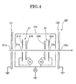
- FIG. 4 shows the structure of another example of a charged particle beam reflector 120.
- the charged particle beam reflector 120 additionally comprises, around the outer periphery of the first and second electrostatic mirrors 21, 22, a decelerator 123 ( FIG. 4 ) decelerating the speed of an electron passing through the electrostatic mirror system by making the entire mirror system have a negative potential.
- Disposed ahead and behind the decelerator 123 are an earth electrode 121 with a through hole 121 a through which the electron beam passes and an earth electrode 122 with a through hole 122a through which the electron beam passes, respectively.
- the decelerator 123 is preferably configured to be applied with a constant voltage V3 whose potential is substantially equal to that of the accelerated voltage of the electron guns 11, 51, thereby to make the potential of the entire mirror system substantially equal to that of the accelerated voltage. This makes it possible to achieve a reflex action of the first and second electrostatic mirrors 21, 22 at a lower voltage and to heighten the speed of reflection and traveling of the electron beam by the first and second electrostatic mirrors.
- Electrostatic mirrors in three or more stages can be also used to reflect the electron beam three times or more.
- first and second electrostatic mirrors are each configured to include a single electrode. However, they can be configured to have a plurality of electrodes, or an electrode which generates a superimposed magnetic field.
- the position of the charged particle beam reflector 20 in the electron microscope is not limited to the position shown in FIGs. 1 , 3 . It can be disposed at any position. However, it is preferable to dispose it at a position closest to the objective lens so as to correct the aberration thereof most effectively.
- the charged particle beam reflector device according to the present invention can be combined with a hexapole.
- the level of accuracy required for the corrector using a multi-pole to correct the chromatic aberration is higher by one digit than to correct the spherical aberration. Therefore, the charged particle beam reflector device can be combined with the multi-pole to correct the chromatic aberration by the charged particle beam reflector device and correct the spherical aberration by the corrector with the multi-pole.
- the present invention is not limited thereto.
- Proton beam or ion beam is also applicable.
- the second electrodes 21 B, 22B of the first and second electrostatic mirrors 21, 22 need to be set to be with a positive potential higher than that of the first electrodes 21A, 22A.
- the above embodiments have described a charged particle beam reflector device which is incorporated into a scan or transmission type electron microscope.
- the present invention is not limited thereto. It is also applicable to a semiconductor manufacture/inspection device using a charged particle beam, an electron beam exposure device, an ion implanter or the like.
Landscapes
- Chemical & Material Sciences (AREA)
- Analytical Chemistry (AREA)
- Analysing Materials By The Use Of Radiation (AREA)
- Electron Sources, Ion Sources (AREA)
Abstract
Description
- The present invention relates to a charged particle beam reflector which can correct chromatic aberration and spherical aberration of a lens system, and to an electron microscope incorporating the charged particle beam reflector.
- Generally, an electron beam used in an electron microscope has a wavelength of 0.024Å when the acceleration voltage is 200kV, for example. It is theoretically possible to increase a resolution of an electron microscope to the order of the wavelength of the electron beam; however, in practice a resolution of the electron microscope is 1.9 Å at most owing to chromatic aberration and spherical aberration of a lens system.
- It is known that the chromatic aberration and spherical aberration of the lens system can be corrected by use of an electrostatic mirror. Japanese Laid-open Patent Application Publication No.
Hei 5-205687 - However, there is a problem in such an electron microscope that since the electron beam is deflected at 90 degrees by the beam deflector, electric and magnetic fields of the beam are both not rotationally symmetric, and the fringing effect of both fields is likely to cause an asymmetric high-order aberration.
- Particularly, the high-order aberration occurring in reality and that theoretically obtained do not always coincide with each other, so that it is hard to suppress the high-order aberration and improve the resolution of the electron microscope to the order of the wavelength of the electron.
- In view of solving the above problem, an object of the present invention is to provide a charged particle beam reflector device which can correct the chromatic aberration and spherical aberration of a lens system without causing high-order aberration due to the fringing effect, and to provide an electron microscope incorporating such a charged particle beam reflector device.
- According to one aspect of the present invention, a charged particle beam reflector device comprises: at least two electrostatic mirrors arranged with a predetermined interval on a linear optical axis, each having a through hole through which a charged particle beam radiated from a charged particle beam source along the linear optical axis passes, and having a function of either of reflecting the charged particle beam and allowing the charged particle beam to pass through the through hole in accordance with an applied voltage; and a voltage controller controlling an applied voltage to the at least two electrostatic mirrors, in which the voltage controller applies a reflection voltage to each of the electrostatic mirrors at a predetermined timing so that the charged particle beam from the charged particle beam source is reflected by the at least two electrostatic mirrors at least more than once, the reflection voltage allowing the electrostatic mirrors to reflect the charged particle beam, numbers of times of the reflections by the respective electrostatic mirrors being the same.
- Preferably, in such a charged particle beam reflector device, one of the electrostatic mirrors is a first electrostatic mirror which is disposed on a side of the charged particle beam source, and the other of the electrostatic mirrors is a second electrostatic mirror facing the first electrostatic mirror. Further, the voltage controller is configured to apply a pass voltage to the first electrostatic mirror at a first timing, applies a second reflection voltage to the second electrostatic mirror at a second timing, and applies a first reflection voltage to the first electrostatic mirror at a third timing, the pass voltage allowing the first electrostatic mirror to have the charged particle beam pass therethrough, the first and second reflection voltage allowing the first and second electrostatic mirrors to reflect the charged particle beam, respectively. The second timing is set to come before the charged particle beam having passed through the through hole of the first electrostatic mirror applied with the pass voltage at the first timing reaches the second electrostatic mirror. The third timing is set to come before the charged particle beam reflected by the second electrostatic mirror reaches the first electrostatic mirror, and the charged particle beam from the charged particle beam source is reflected by the first and second electrostatic mirrors at least more than once, the number of times of the reflections by the first and second electrostatic mirrors being the same.
- Preferably, such a charged particle beam reflector device further comprises a decelerator around an outer periphery of each of the electrostatic mirrors, to decelerate the charged particle beam.
- According to another aspect of the present invention, an electron microscope comprises the above charged particle beam reflector device, a charged particle beam source radiating a charged particle beam along a linear optical axis, a convergent lens, and an objective lens.
- Preferably, the electron microscope is set so that the charged particle beam is radiated as a pulse from the charged particle beam reflector device, in which the electron beam scans via the objective lens with a scan period and a blanking period, and a period in which the pulse is not outputted and the blanking period are made coincident with each other.
- Advantageously, the charged particle beam reflector device according to the present invention is configured to include at least the first and second electrostatic mirrors with the through holes so as to achieve the function of reflecting the charged particle beam or allowing it to pass through the through holes. With such configuration, it can correct the chromatic aberration and the spherical aberration separately without causing the high-order aberration due to the fringing effect.
-
-
FIG. 1 shows a structure of an electron microscope according to a first embodiment of the present invention; -
FIG. 2 is a timing chart for operation of a charged particle beam reflector inFIG. 1 ; -
FIG. 3 shows a structure of an electron microscope according to a second embodiment of the present invention; and -
FIG. 4 shows a structure of an electron microscope according to a third embodiment of the present invention. - Hereinafter, embodiments of an electron microscope comprising a charged particle beam reflector device according to the present invention will be described in detail with reference to the accompanying drawings.
-
FIG. 1 shows a scantype electron microscope 10. The electron microscope comprises an electron gun (charged particle beam source) 11 radiating an electron beam as a charged particle beam along a linearoptical axis 10A, a firstconvergent lens 12 and a secondconvergent lens 13 converging the radiated electron beam, anobjective lens 14 irradiating an electron beam to aspecimen 18, a chargedparticle beam reflector 20 provided between the secondconvergent lens 13 and theobjective lens 14,polarizers particle beam reflector 20 and theobjective lens 14 for scanning with the electron beam, and asecondary electron detector 17 provided between thespecimen 18 and theobjective lens 14. - The
electron gun 11 radiates an electron beam at an acceleration voltage of 1 to 3kV, for example. - The charged
particle beam reflector 20 includes first and secondelectrostatic mirrors optical axis 10A with a predetermined interval. - The first
electrostatic mirror 21 includes afirst electrode 21A on a side of theelectron gun 11, asecond electrode 21B applied with a voltage of a lower potential than that of thefirst electrode 21A, and a throughhole 21 a formed through the first andsecond electrodes optical axis 10A passes. Likewise, the secondelectrostatic mirror 22 includes afirst electrode 22A, asecond electrode 22B applied with a voltage of a lower potential than that of thefirst electrode 22A, and a throughhole 22a formed through the first andsecond electrodes optical axis 10A passes. The first and second electrodes of the first and secondelectrostatic mirrors first electrodes - A
controller 30 controls applied voltages to the first and secondelectrostatic mirrors controller 30 and chargedparticle beam reflector 20 constitute the charged particle beam reflector device. - Next, the operation of the
electron microscope 10 as configured above will be described with reference to a timing chart inFIG. 2 . - An electron beam as charged particles is radiated from the
electron gun 11, travels along the linearoptical axis 10A, and passes through the first and secondconvergent lenses electrostatic mirror 21 of the charged particle beam reflector 20 (first timing), thecontroller 30 applies a pass voltage V1T whose absolute value is smaller than an accelerated voltage value to the firstelectrostatic mirror 21 to have the electron beam pass through the throughhole 21 a thereof. - Before the electron beam having passed through the through
hole 21 a reaches the second electrostatic mirror 22 (second timing), thecontroller 30 applies a reflection voltage V2R whose absolute value is larger than an accelerated voltage value to the secondelectrostatic mirror 22 to have the electron beam reflected by the secondelectrostatic mirror 22. - Then, before the electron beam reflected by the second
electrostatic mirror 22 reaches the first electrostatic mirror 21 (third timing), thecontroller 30 applies a reflection voltage V1R whose absolute value is larger than an accelerated voltage value to the firstelectrostatic mirror 21 to have the electron beam reflected by the firstelectrostatic mirror 21. - Before the electron beam reflected by the first
electrostatic mirror 21 reaches the second electrostatic mirror 22 (fourth timing), thecontroller 30 applies a pass voltage V2T whose absolute value is smaller than an accelerated voltage value to the secondelectrostatic mirror 22 to have the electron beam pass through the throughhole 22a thereof. - Through repetition of a series of operation above, the electron beam is emitted from the charged
particle beam reflector 20 in a pulse P form with a predetermined cycle, as shown inFIG. 2 . - In
FIG. 2 , time t1 represents a time from the electron beam's having passed through the firstelectrostatic mirror 21 to its reaching the secondelectrostatic mirror 22, a time t2 represents a time from the electron beam's being reflected by the secondelectrostatic mirror 22 to its reaching the firstelectrostatic mirror 21, a time t3 represents a time from the electron beam's being reflected by the secondelectrostatic mirror 22 to its reaching the firstelectrostatic mirror 21. The times t1 to t3 change depending on the distance between the first andelectrostatic mirrors - In the timing chart of
FIG. 2 , the firstelectrostatic mirror 21 is applied with the pass voltage V1T between a first timing and a third timing while the secondelectrostatic mirror 22 is applied with the reflection voltage V2R between a second timing and a fourth timing. The voltage applied to the first and secondelectrostatic mirrors - The applied voltage to the
polarizers particle beam reflector 20, in accordance with the pulse width of the electron beam. The electron beam scans thespecimen 18 via theobjective lens 14. That is, the applied voltage to thepolarizers specimen 18 efficiently. - Here, in the charged
particle beam reflector 20 the electron beam is merely reflected in parallel by the first and secondelectrostatic mirrors objective lens 14 or the like by the reflection by the first and second electrostatic mirrors without the high-order aberration caused by the fringing effect. - The faster the electron travels, the larger the amount it travels until it reaches the electrostatic mirror and is reflected thereby. Such an electron will be more greatly affected by action of the electrostatic mirror, resulting in correcting the chromatic aberration.
- The spherical aberration can be corrected with use of the electrostatic mirror by making the electron beam reflected by the electrostatic mirror incident on the
objective lens 14 or the like and canceling out a negative spherical aberration by the electrostatic mirror and a positive spherical aberration by theobjective lens 14. - According to the first embodiment, the electron beam is reflected by each of the first and second
electrostatic mirrors -
FIG. 3 shows a transmission-type electron microscope 50 incorporating a charged particle beam reflector device. Theelectron microscope 50 comprises anelectron gun 51 radiating an electron beam as charged particle beam along a linearoptical axis 50A, a firstconvergent lens 52 and a secondconvergent lens 57 converging the radiated electron beam, anobjective lens 53, anintermediate lens 56, aprojector lens 54, afluorescent plate 55, and a chargedparticle beam reflector 20 provided between theobjective lens 53 and theintermediate lens 56. Note that thefluorescent plate 55 can be a CCD detector. - In
FIG. 3 , the chargedparticle beam reflector 20 as an electrostatic mirror correction system is disposed between theobjective lens 53 and theintermediate lens 56, however, it can be disposed between theintermediate lens 56 and theprojector lens 54. - Similarly to the first embodiment, a period between two pulses is set to coincide with the blanking period of the electron, when there is a blanking period. This enables efficient irradiation of the electron beam to the
specimen 18. - The
electron microscope 50 can correct the chromatic aberration and spherical aberration of theobjective lens 53 without causing high-order aberration due to the fringing effect, as in the first embodiment -
FIG. 4 shows the structure of another example of a chargedparticle beam reflector 120. The chargedparticle beam reflector 120 additionally comprises, around the outer periphery of the first and secondelectrostatic mirrors FIG. 4 ) decelerating the speed of an electron passing through the electrostatic mirror system by making the entire mirror system have a negative potential. Disposed ahead and behind thedecelerator 123 are anearth electrode 121 with a throughhole 121 a through which the electron beam passes and anearth electrode 122 with a throughhole 122a through which the electron beam passes, respectively. - The
decelerator 123 is preferably configured to be applied with a constant voltage V3 whose potential is substantially equal to that of the accelerated voltage of theelectron guns electrostatic mirrors - The above embodiments have described an example where two-stage electrostatic mirrors are used, however, the present invention is not limited thereto. Electrostatic mirrors in three or more stages can be also used to reflect the electron beam three times or more.
- Further, the first and second electrostatic mirrors are each configured to include a single electrode. However, they can be configured to have a plurality of electrodes, or an electrode which generates a superimposed magnetic field.
- The position of the charged
particle beam reflector 20 in the electron microscope is not limited to the position shown inFIGs. 1 ,3 . It can be disposed at any position. However, it is preferable to dispose it at a position closest to the objective lens so as to correct the aberration thereof most effectively. - Moreover, there is a known aberration corrector with a multi-pole (hexapole, for example). The charged particle beam reflector device according to the present invention can be combined with a hexapole. The level of accuracy required for the corrector using a multi-pole to correct the chromatic aberration is higher by one digit than to correct the spherical aberration. Therefore, the charged particle beam reflector device can be combined with the multi-pole to correct the chromatic aberration by the charged particle beam reflector device and correct the spherical aberration by the corrector with the multi-pole.
- The above embodiments have described an example of using an electron beam for the charged particle, however, the present invention is not limited thereto. Proton beam or ion beam is also applicable. With use of a positively charged particle beam such as proton beam, the
second electrodes electrostatic mirrors first electrodes - The above embodiments have described a charged particle beam reflector device which is incorporated into a scan or transmission type electron microscope. However, the present invention is not limited thereto. It is also applicable to a semiconductor manufacture/inspection device using a charged particle beam, an electron beam exposure device, an ion implanter or the like.
- It should be appreciated that variations may be made in the embodiments described by those skilled in the art without departing from the scope of the present invention as defined by the following claims.
Claims (5)
- A charged particle beam reflector device comprising:at least two electrostatic mirrors (21, 22) arranged with a predetermined interval on a linear optical axis (10A, 50A), each having a through hole (21 a, 22a) through which a charged particle beam radiated from a charged particle beam source (11, 51) along the linear optical axis (10A, 50A) passes, and having a function of either reflecting the charged particle beam or allowing the charged particle beam to pass through the through hole (21 a, 22a) in accordance with an applied voltage; anda voltage controller (30) controlling an applied voltage to the at least two electrostatic mirrors (21, 22), whereinthe voltage controller applies a reflection voltage (V1R, V2R) to each of the electrostatic mirrors (21, 22) at a predetermined timing so that the charged particle beam from the charged particle beam source (11, 51) is reflected by each of the electrostatic mirrors (21, 22) at least more than once, the reflection voltage (V1R, V2R) allowing the electrostatic mirrors (21, 22) to reflect the charged particle beam, numbers of times of the reflections by the respective electrostatic mirrors (21, 22) being the same.
- A charged particle beam reflector device according to claim 1, wherein:one of the electrostatic mirrors is a first electrostatic mirror (21) which is disposed on a side of the charged particle beam source (11, 51);the other of the electrostatic mirrors is a second electrostatic mirror (22) facing the first electrostatic mirror (21);the voltage controller (30) is configured to apply a pass voltage (V1T) to the first electrostatic mirror (21) at a first timing, applies a second reflection voltage (V2R) to the second electrostatic mirror (22) at a second timing, and applies a first reflection voltage (V1R) to the first electrostatic mirror (21) at a third timing, the pass voltage (V1T) allowing the first electrostatic mirror (21) to have the charged particle pass therethrough, the first and second reflection voltages (V1R, V2R) allowing the first and second electrostatic mirrors (21, 22) to reflect the charged particle beam, respectively;the second timing is set to come before the charged particle beam having passed through the through hole (21 a) of the first electrostatic mirror (21) applied with the pass voltage (V1T) at the first timing reaches the second electrostatic mirror (22);the third timing is set to come before the charged particle beam reflected by the second electrostatic mirror (22) reaches the first electrostatic mirror (21); andthe charged particle beam from the charged particle beam source (11, 51) is reflected by the first and second electrostatic mirrors (21, 22) at least more than once, numbers of times of the reflections by the first and second electrostatic mirrors (21, 22) being the same.
- A charged particle beam reflector device according to claim 1 or claim 2, further comprising a decelerator (123) around an outer periphery of the electrostatic mirrors (21, 22), the decelerator (123) decelerating the charged particle beam.
- An electron microscope comprising:the charged particle beam reflector device according to any of claims 1 to claim 3;a charged particle beam source (11, 51) radiating a charged particle beam along a linear optical axis (10A, 50A);a convergent lens (12, 13, 52, 57); andan objective lens (14, 53).
- An electron microscope according to claim 4, wherein
the electron microscope is set so that the charged particle beam is radiated as a pulse from the charged particle beam reflector device; wherein the electron beam scans via the objective lens (14, 53) with a scan period and a blanking period; and wherein a period in which the pulse is not outputted and the blanking period are made coincident with each other.
Applications Claiming Priority (1)
| Application Number | Priority Date | Filing Date | Title |
|---|---|---|---|
| JP2007266053A JP2009094020A (en) | 2007-10-12 | 2007-10-12 | Charged particle beam reflector and electron microscope |
Publications (2)
| Publication Number | Publication Date |
|---|---|
| EP2048690A2 true EP2048690A2 (en) | 2009-04-15 |
| EP2048690A3 EP2048690A3 (en) | 2010-12-15 |
Family
ID=40227733
Family Applications (1)
| Application Number | Title | Priority Date | Filing Date |
|---|---|---|---|
| EP08253293A Withdrawn EP2048690A3 (en) | 2007-10-12 | 2008-10-09 | Charged particle beam reflector device and electron microscope |
Country Status (3)
| Country | Link |
|---|---|
| US (1) | US7902504B2 (en) |
| EP (1) | EP2048690A3 (en) |
| JP (1) | JP2009094020A (en) |
Families Citing this family (4)
| Publication number | Priority date | Publication date | Assignee | Title |
|---|---|---|---|---|
| US9406479B1 (en) * | 2015-06-25 | 2016-08-02 | Electron Optica, Inc. | Mirror pulse compressor for electron beam apparatus |
| NL2017213B1 (en) | 2016-07-22 | 2018-01-30 | Univ Delft Tech | Aberration correcting device for an electron microscope and an electron microscope comprising such a device |
| US10283315B2 (en) | 2017-05-16 | 2019-05-07 | International Business Machines Corporation | Measuring spherical and chromatic aberrations in cathode lens electrode microscopes |
| JP7328477B2 (en) * | 2018-11-16 | 2023-08-17 | 株式会社北海光電子 | photoelectron microscope |
Citations (1)
| Publication number | Priority date | Publication date | Assignee | Title |
|---|---|---|---|---|
| JPH05205687A (en) | 1991-09-04 | 1993-08-13 | Carl Zeiss:Fa | Image-forming system, for changed elementary particle beams use, equipped with mirror corrector |
Family Cites Families (9)
| Publication number | Priority date | Publication date | Assignee | Title |
|---|---|---|---|---|
| DE3025764C2 (en) * | 1980-07-08 | 1984-04-19 | Hermann Prof. Dr. 6301 Fernwald Wollnik | Time of flight mass spectrometer |
| JPH01264161A (en) * | 1988-04-14 | 1989-10-20 | Hitachi Ltd | Secondary ion mass spectrometer |
| US6107625A (en) * | 1997-05-30 | 2000-08-22 | Bruker Daltonics, Inc. | Coaxial multiple reflection time-of-flight mass spectrometer |
| US6013913A (en) * | 1998-02-06 | 2000-01-11 | The University Of Northern Iowa | Multi-pass reflectron time-of-flight mass spectrometer |
| DE10116536A1 (en) * | 2001-04-03 | 2002-10-17 | Wollnik Hermann | Flight time mass spectrometer has significantly greater ion energy on substantially rotation symmetrical electrostatic accelerating lens axis near central electrodes than for rest of flight path |
| US7385187B2 (en) * | 2003-06-21 | 2008-06-10 | Leco Corporation | Multi-reflecting time-of-flight mass spectrometer and method of use |
| JP2005150058A (en) * | 2003-11-20 | 2005-06-09 | Canon Inc | Liquid metal ion emission apparatus, ion beam irradiation apparatus, processing apparatus equipped with the ion beam irradiation apparatus, analysis apparatus, and method of manufacturing liquid metal ion emission apparatus |
| GB2428868B (en) * | 2005-10-28 | 2008-11-19 | Thermo Electron Corp | Spectrometer for surface analysis and method therefor |
| JP5250350B2 (en) * | 2008-09-12 | 2013-07-31 | 株式会社日立ハイテクノロジーズ | Charged particle beam application equipment |
-
2007
- 2007-10-12 JP JP2007266053A patent/JP2009094020A/en active Pending
-
2008
- 2008-10-09 EP EP08253293A patent/EP2048690A3/en not_active Withdrawn
- 2008-10-10 US US12/285,673 patent/US7902504B2/en not_active Expired - Fee Related
Patent Citations (1)
| Publication number | Priority date | Publication date | Assignee | Title |
|---|---|---|---|---|
| JPH05205687A (en) | 1991-09-04 | 1993-08-13 | Carl Zeiss:Fa | Image-forming system, for changed elementary particle beams use, equipped with mirror corrector |
Also Published As
| Publication number | Publication date |
|---|---|
| US20090095904A1 (en) | 2009-04-16 |
| US7902504B2 (en) | 2011-03-08 |
| EP2048690A3 (en) | 2010-12-15 |
| JP2009094020A (en) | 2009-04-30 |
Similar Documents
| Publication | Publication Date | Title |
|---|---|---|
| JP4037533B2 (en) | Particle beam equipment | |
| TWI476807B (en) | Drawing apparatus and method of manufacturing article | |
| JP4900389B2 (en) | Spherical aberration correction decelerating lens, spherical aberration correction lens system, electron spectrometer, and photoelectron microscope | |
| JP2000133194A5 (en) | ||
| JP2007500948A5 (en) | ||
| US8957392B2 (en) | Mass spectrometer | |
| JP2010067530A (en) | Charged particle beam apparatus | |
| JP2015032360A (en) | Electron beam equipment | |
| US7902504B2 (en) | Charged particle beam reflector device and electron microscope | |
| JP6690050B2 (en) | Aberration correction device for electron microscope and electron microscope equipped with such device | |
| JP2006080155A (en) | Electron beam application equipment | |
| JP5452722B2 (en) | Aberration correction apparatus and charged particle beam apparatus using the same | |
| JP6401600B2 (en) | Streak tube and streak device including the same | |
| JP2011023126A (en) | Charged particle beam irradiating device, lithography apparatus, analyzer microscope, charged particle beam emitter, and lens unit for charged particle beam | |
| JP3862344B2 (en) | Electrostatic lens | |
| WO2013073373A1 (en) | Mass distribution spectrometry method and mass distribution spectrometer | |
| EP2775504A1 (en) | Streak tube and streak device including same | |
| JP3649008B2 (en) | Electron beam equipment | |
| JP5934517B2 (en) | Chromatic aberration corrector and control method for chromatic aberration corrector | |
| JP3790646B2 (en) | Low energy reflection electron microscope | |
| KR20120128105A (en) | Drawing apparatus and method of manufacturing article | |
| JP3915812B2 (en) | Electron beam equipment | |
| WO2024134945A1 (en) | Streak tube | |
| JPH03102813A (en) | Variable forming type charged particle beam exposure apparatus | |
| JPH04206131A (en) | Device for obtaining specimen image based on electron |
Legal Events
| Date | Code | Title | Description |
|---|---|---|---|
| PUAI | Public reference made under article 153(3) epc to a published international application that has entered the european phase |
Free format text: ORIGINAL CODE: 0009012 |
|
| AK | Designated contracting states |
Kind code of ref document: A2 Designated state(s): AT BE BG CH CY CZ DE DK EE ES FI FR GB GR HR HU IE IS IT LI LT LU LV MC MT NL NO PL PT RO SE SI SK TR |
|
| AX | Request for extension of the european patent |
Extension state: AL BA MK RS |
|
| PUAL | Search report despatched |
Free format text: ORIGINAL CODE: 0009013 |
|
| AK | Designated contracting states |
Kind code of ref document: A3 Designated state(s): AT BE BG CH CY CZ DE DK EE ES FI FR GB GR HR HU IE IS IT LI LT LU LV MC MT NL NO PL PT RO SE SI SK TR |
|
| AX | Request for extension of the european patent |
Extension state: AL BA MK RS |
|
| RIC1 | Information provided on ipc code assigned before grant |
Ipc: H01J 49/40 20060101ALI20101108BHEP Ipc: H01J 37/28 20060101ALI20101108BHEP Ipc: H01J 37/26 20060101ALI20101108BHEP Ipc: H01J 37/153 20060101AFI20090120BHEP |
|
| AKY | No designation fees paid | ||
| REG | Reference to a national code |
Ref country code: DE Ref legal event code: R108 |
|
| REG | Reference to a national code |
Ref country code: DE Ref legal event code: R108 Effective date: 20110824 |
|
| STAA | Information on the status of an ep patent application or granted ep patent |
Free format text: STATUS: THE APPLICATION IS DEEMED TO BE WITHDRAWN |
|
| 18D | Application deemed to be withdrawn |
Effective date: 20110616 |