EP2045579A2 - Photodiode array for an optical encoder and optical encoder - Google Patents
Photodiode array for an optical encoder and optical encoder Download PDFInfo
- Publication number
- EP2045579A2 EP2045579A2 EP08015899A EP08015899A EP2045579A2 EP 2045579 A2 EP2045579 A2 EP 2045579A2 EP 08015899 A EP08015899 A EP 08015899A EP 08015899 A EP08015899 A EP 08015899A EP 2045579 A2 EP2045579 A2 EP 2045579A2
- Authority
- EP
- European Patent Office
- Prior art keywords
- pitch
- photodiode
- photodiodes
- optical encoder
- detector array
- Prior art date
- Legal status (The legal status is an assumption and is not a legal conclusion. Google has not performed a legal analysis and makes no representation as to the accuracy of the status listed.)
- Withdrawn
Links
- 230000003287 optical effect Effects 0.000 title claims abstract description 23
- 230000000295 complement effect Effects 0.000 claims description 24
- 239000011295 pitch Substances 0.000 description 115
- 238000004519 manufacturing process Methods 0.000 description 11
- 238000006073 displacement reaction Methods 0.000 description 8
- 238000003491 array Methods 0.000 description 5
- 238000000034 method Methods 0.000 description 4
- 239000000758 substrate Substances 0.000 description 3
- 238000005259 measurement Methods 0.000 description 2
- 238000001514 detection method Methods 0.000 description 1
Images


Classifications
-
- G—PHYSICS
- G01—MEASURING; TESTING
- G01D—MEASURING NOT SPECIALLY ADAPTED FOR A SPECIFIC VARIABLE; ARRANGEMENTS FOR MEASURING TWO OR MORE VARIABLES NOT COVERED IN A SINGLE OTHER SUBCLASS; TARIFF METERING APPARATUS; MEASURING OR TESTING NOT OTHERWISE PROVIDED FOR
- G01D5/00—Mechanical means for transferring the output of a sensing member; Means for converting the output of a sensing member to another variable where the form or nature of the sensing member does not constrain the means for converting; Transducers not specially adapted for a specific variable
- G01D5/26—Mechanical means for transferring the output of a sensing member; Means for converting the output of a sensing member to another variable where the form or nature of the sensing member does not constrain the means for converting; Transducers not specially adapted for a specific variable characterised by optical transfer means, i.e. using infrared, visible, or ultraviolet light
- G01D5/32—Mechanical means for transferring the output of a sensing member; Means for converting the output of a sensing member to another variable where the form or nature of the sensing member does not constrain the means for converting; Transducers not specially adapted for a specific variable characterised by optical transfer means, i.e. using infrared, visible, or ultraviolet light with attenuation or whole or partial obturation of beams of light
- G01D5/34—Mechanical means for transferring the output of a sensing member; Means for converting the output of a sensing member to another variable where the form or nature of the sensing member does not constrain the means for converting; Transducers not specially adapted for a specific variable characterised by optical transfer means, i.e. using infrared, visible, or ultraviolet light with attenuation or whole or partial obturation of beams of light the beams of light being detected by photocells
- G01D5/36—Forming the light into pulses
-
- G—PHYSICS
- G01—MEASURING; TESTING
- G01D—MEASURING NOT SPECIALLY ADAPTED FOR A SPECIFIC VARIABLE; ARRANGEMENTS FOR MEASURING TWO OR MORE VARIABLES NOT COVERED IN A SINGLE OTHER SUBCLASS; TARIFF METERING APPARATUS; MEASURING OR TESTING NOT OTHERWISE PROVIDED FOR
- G01D5/00—Mechanical means for transferring the output of a sensing member; Means for converting the output of a sensing member to another variable where the form or nature of the sensing member does not constrain the means for converting; Transducers not specially adapted for a specific variable
- G01D5/26—Mechanical means for transferring the output of a sensing member; Means for converting the output of a sensing member to another variable where the form or nature of the sensing member does not constrain the means for converting; Transducers not specially adapted for a specific variable characterised by optical transfer means, i.e. using infrared, visible, or ultraviolet light
- G01D5/32—Mechanical means for transferring the output of a sensing member; Means for converting the output of a sensing member to another variable where the form or nature of the sensing member does not constrain the means for converting; Transducers not specially adapted for a specific variable characterised by optical transfer means, i.e. using infrared, visible, or ultraviolet light with attenuation or whole or partial obturation of beams of light
- G01D5/34—Mechanical means for transferring the output of a sensing member; Means for converting the output of a sensing member to another variable where the form or nature of the sensing member does not constrain the means for converting; Transducers not specially adapted for a specific variable characterised by optical transfer means, i.e. using infrared, visible, or ultraviolet light with attenuation or whole or partial obturation of beams of light the beams of light being detected by photocells
- G01D5/347—Mechanical means for transferring the output of a sensing member; Means for converting the output of a sensing member to another variable where the form or nature of the sensing member does not constrain the means for converting; Transducers not specially adapted for a specific variable characterised by optical transfer means, i.e. using infrared, visible, or ultraviolet light with attenuation or whole or partial obturation of beams of light the beams of light being detected by photocells using displacement encoding scales
- G01D5/34707—Scales; Discs, e.g. fixation, fabrication, compensation
- G01D5/34715—Scale reading or illumination devices
Definitions
- the present invention relates to a photodiode array for an optical encoder and to an optical encoder.
- Encoders are used to measure angular or linear displacement.
- Optical encoders include photodiode arrays arranged in a detection plane for detecting incremental signals indicative of relative movement, e.g., rotary or linear movement, of encoder parts.
- Optical encoders include a light source, a scale index member (such as, e.g., a slotted or graduated code disk), and an array of photodiodes.
- a graduated code disk includes alternating transparent and opaque areas arranged periodically in a defined, fixed code disk pitch. In rotary encoders, the code disk is typically coupled to a rotating shaft and moved relative to the light source and the photodiode array.
- Light is directed from the light source to the photodiode array by the scale index member or code disk.
- the code disk rotates, in the case of an angular encoder, or moves linearly, in the case of a linear encoder, output signals from the photodiode array change: These varying output signals are used to measure angular or linear displacement.
- An encoder's resolution refers to how sensitive the encoder is to displacement and depends on the amount of displacement between discrete measurement points.
- An encoder with a higher resolution allows more precise displacement measurement than encoders with lower resolutions.
- Increasing resolution may be complicated by manufacturing limitations, such as, e.g., a minimum width of the individual photodiodes and a minimum distance between adjacent, i.e., immediately adjacent, photodiodes. For example, under certain manufacturing constraints, it may not be possible to manufacture diodes having a pitch below, e.g., 9 ⁇ m
- U.K. Published Patent Application 2 353 810 relates to a displacement measuring apparatus.
- the photodiodes are deposited onto a substrate in two or more separate layers with adjacent photodiodes being deposited in different layers. This process may allow adjacent photodiodes to be more closely spaced than if the photodiodes were all deposited in the same layer.
- manufacture of such an apparatus requires complex sensor fabrication techniques, additional layers and interconnects, thereby resulting in increased manufacturing costs.
- a photodiode detector array for an optical encoder includes: a sequence of photodiodes having a pitch between adjacent, i.e., immediately adjacent, photodiodes that alternates between a first pitch and a second pitch, the second pitch being different than the first pitch.
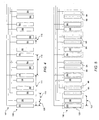
- Figure 1 is a top view of a conventional photodiode detector array 10.
- the photodiode detector array 10 includes a pattern of repeating segments of four photodiodes 3A, 4A, 3B, 4B.
- the photodiodes include two pairs of complementary photodiodes, the first pair including photodiodes 3A and 3B and the second pair including photodiodes 4A and 4B.
- An output arrangement 11 includes four discrete output signals, one for each of the four photodiodes 3A, 4A, 3B, 4B included in each repeating segment. Each output signal of a repeating segment is connected in series to corresponding output signals of other segments.
- FIG. 1 is a top view of the photodiode array 10 illustrated in Figure 1 , further illustrating the scale of the code disk. In Figure 2 , the scale is indicated by slots 18. These slots 18 may be, e.g., openings in the code disk, alternating opaque/transparent areas of the code disk, alternating reflective/non-reflective areas of the code disk, etc.
- the slots direct light from a light source to the photodiodes 3A, 4A, 3B, 4B.
- the slots 18 are positioned according to a code disk pitch 20, which, in this example, is constant and is four times the photodiode pitch 14. When the slots 18 are in the position indicated in Figure 2 , each slot 18 fully exposes each photodiode 3A to light from the light source, while photodiode 3B is unexposed, and photodiodes 4A and 4B are each approximately half exposed.
- Signal 30A the output signal from photodiodes 3A
- signal 30B the output signal from photodiodes 3B
- Signals 40A and 40B the output signals from photodiodes 4A and 4B, respectively, are each approximately at a value halfway between a maximum value and a minimum value.
- the signals 30A, 30B, 40A, 40B are sinusoidal.
- signal 30A is at a maximum positive value
- signal 30B is at a maximum negative value
- each of signals 40A, 40B is at a zero value.
- Channel 30C is at a high value when the value of signal 30A exceeds the value of signal 30B and at a low value when the value of signal 30B exceeds the value of signal 30A; and channel 40C is at a high value when the value of signal 40A exceeds the value of signal 40B and at a low value when the value of signal 40B exceeds the value of signal 40A.
- the slots 18 are displaced in relation to the photodiode array 10 by a distance equal to the pitch 20, four discrete position signal combinations 46, 47, 48, 49 are successively generated.
- the resolution of the photodiode array 10 illustrated in Figures 1 and 2 may -- in theory -- be increased indefinitely by reducing the width of the photodiodes 3A, 4A, 3B, 4B, the gap 15 between the photodiodes, and the pitch 20 between slots 18.
- the resolution of this array 10 is subject to real-world manufacturing limitations.
- the minimum pitch 14 achievable between adjacent photodiodes may be, e.g., 9.0 ⁇ m
- the minimum gap 15 between adjacent photodiodes may be, e.g., 5.0 ⁇ m.
- Example embodiments of the present invention provide for a photodiode array having a virtual diode pitch that is less than the actual minimum pitch manufacturable by the manufacturing process.
- a photodiode array according to example embodiments of the present invention may provide for a virtual diode pitch of, e.g., 4.5 ⁇ m. That is, example embodiments of the present invention provide for greater resolution as compared with conventional devices.
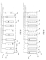
- FIG. 4 is a top view of a photodiode detector array 100 according to an exemplary embodiment of the present invention.
- the photodiode detector array 100 includes a pattern of repeating segments of eight photodiodes, each segment having the following pattern: 5A, 5B, 6A, 6B, 5B, 5A, 6B, 6A.
- four pairs of complementary photodiodes e.g., 5A-5B, 6A-6B, 5B-5A, and 6B-6A, each have a first pitch 105 and a gap 115 between complements, and a second pitch 110 between adjacent complementary pairs.
- the second pitch 110 is 1.5 times the first pitch 105.
- each complementary photodiode 5A, 5B, 6A, 6B repeats with a pitch that alternates between six times the first pitch 105 and four times the first pitch 105.
- photodiode 5A repeats with a pitch that alternates between a first distance 111 that is six times the first pitch 105 and a second distance 112 that is four times the first pitch 105.
- FIG. 5 is a top view of the photodiode detector array 100 illustrated in Figure 4 , further illustrating the positions of slots 120 of a scale index member, e.g., a code disk.
- These slots 120 direct light from a light source to the photodiodes 5A, 5B, 6A, 6B.
- the slots 120 are positioned according to a constant slot pitch 125, which, in this example, is twice the first pitch 105.
- each photodiode 5A is fully exposed by the slots 120 to light from the light source, while photodiode 5B is substantially unexposed and photodiodes 6A and 6B are each approximately half exposed.
- the slots exposing photodiodes 5A are alternatingly spaced by distances equal to three and two times the slot pitch 125.
- the array 100 illustrated in Figures 4 and 5 may have a virtual resolution of twice that of the array 10 illustrated in Figures 1 and 2 .
- FIG. 6 is a top view of a photodiode detector array 150 according to an exemplary embodiment of the present invention.
- the photodiode detector array 150 includes a pattern of repeating segments of eight photodiodes, each segment having the following pattern: 7A, 7B, 8A, 8B, 7B, 7A, 8B, 8A.
- four pairs of complementary photodiodes e.g., 7A-7B, 8A-8B, 7B-7A, and 8B-8A, each have a first pitch 155 and a gap 165 between complements, and a second pitch 160 between adjacent complementary pairs.
- the second pitch 160 is 7/6, i.e. 1 1/6, times the first pitch 155.
- each complementary photodiode repeats with a pitch that alternates between 5 1/3 times the first pitch 155 and 3 1/3 times the first pitch 155.
- photodiode 7A repeats with a pitch that alternates between a first distance 161 that is 5 1/3 times the first pitch 155 and a second distance 162 that is 3 1/3 times the first pitch 155.
- FIG 7 is a top view of the photodiode detector array 150 illustrated in Figure 6 further illustrating the positions of slots 170 of a scale index member, e.g., a code disk.
- These slots 170 direct light from a light source to the photodiodes 7A, 7B, 8A, 8B.
- the slots 170 are positioned according to a slot pitch 175, which, in this example, is 2/3 times the first pitch 155.
- each photodiode 5A is fully exposed by the slots 170 to light from the light source, while photodiode 5B is substantially unexposed and photodiodes 6A and 6B are each approximately half exposed.
- the slots exposing photodiodes 7A are alternatingly spaced by distances equal to eight and five times the slot pitch 175.
- FIG 8 is a top view of a photodiode detector array 200 according to an exemplary embodiment of the present invention.
- the photodiode detector array 200 includes a pattern of repeating segments of eight photodiodes, each segment having the following pattern: 17A, 19A, 19B, 17A, 17B, 19B, 19A, 17B.
- four non-complementary pairs of photodiodes e.g., 17A-19A, 19B-17A, 17B-19B, and 19A-17B, each have a first pitch 205 and a gap 215 between non-complements, and a second pitch 210 between adjacent non-complementary pairs.
- the second pitch 210 is 1.2 times the first pitch 205.
- each complementary photodiode repeats with a pitch that alternates between 3.2 times the first pitch 205 and 5.6 times the first pitch 205.
- photodiode 17A repeats with a pitch that alternates between a first distance 211 that is 3.2 times the first pitch 205 and a second distance 212 that is 5.6 times the first pitch 205.
- FIG 9 is a top view of the photodiode detector array 200 illustrated in Figure 8 further illustrating the positions of slots 220 of a scale index member, e.g., a code disk.
- These slots 220 direct light from a light source to the photodiodes 17A, 17B, 19A, 19B.
- the slots 220 are positioned according to a slot pitch 225, which, in this example, is 4/5, or 0.8 times, the first pitch 205.
- a slot pitch 225 which, in this example, is 4/5, or 0.8 times, the first pitch 205.
- each photodiode 17A is fully exposed by the slots 220 to light from the light source, while photodiodes 17B are substantially unexposed and photodiodes 19A and 19B are each approximately half exposed.
- the slots exposing photodiodes 17A are alternatingly spaced by distances equal to four and seven times the slot pitch 225.
- the photodiode detector arrays 100, 150, 200 and the slots 120, 170, 220 may be disposed in a nonlinear arrangement, e.g., along a circumference or an arc. It should be further appreciated that the slots 120, 170, 220 may be, e.g., openings, reflectors, or any other configuration that allows for the effective direction of light from a light source to the photodiode detector arrays 100, 150, 200.
- Signal 90A which represents the output signal from: photodiodes 5A, photodiodes 7A, or photodiodes 17A is approximately at a maximum value
- signal 30B which is the output signal from photodiodes 5B, photodiodes 7B, or photodiodes 17B is approximately at a minimum value.
- Signals 95A and 95B which are the output signals from photodiodes 6A and 6B, respectively, photodiodes 8A and 8B, respectively, or photodiodes 19A and 19B, respectively, are each approximately at a value halfway between a maximum value and a minimum value.
- These analog signals 90A, 90B, 95A, 95B are converted to digital channels 90C and 95C.
- Channel 90C is at a high value when the value of signal 90A exceeds the value of signal 90B and at a low value when the value of signal 90B exceeds the value of signal 90A; and channel 95C is at a high value when the value of signal 95A exceeds the value of signal 95B and at a low value when the value of signal 95B exceeds the value of signal 95A.
- Figure 11 is a side view of a portion 180 of an optical encoder, including a light source 181, a slotted scale index member 182, a substrate 183, and a photodiode detector array 184 arranged on the substrate 183.
- the slotted scale index member 182 As the slotted scale index member 182 is displaced with respect to the photodiode detector array 184 and the light source 181, the slotted scale index member 182 directs light from the light source 181 to the photodiode detector array 184 though slots disposed in the slotted scale index member 182.
- first pitch and second pitch may be used according to the foregoing equations by, e.g., adjusting the integer value of i.
- the second diode pitch may be (a) twice the first diode pitch, (b) 1 1/9 the first diode pitch, or (c)1 1/10 the first diode pitch.
- first pitch, second pitch and code disk pitch provide for very high virtual resolution.
- a six-fold increase in resolution e.g., a 6X virtual resolution
- a five-fold increase in resolution e.g., a 5X virtual resolution
- a virtual diode pitch of 1.6 ⁇ m may be attained even though the photodiodes are arranged at a first pitch of 9.6 ⁇ m and at a second pitch of 11.2 ⁇ m (i.e., a 6X virtual resolution); and, for a code disk pitch of 7.2 ⁇ m, a virtual diode pitch of 1.8 ⁇ m may be attained even though the photodiodes are arranged at a first pitch of 9.0 ⁇ m and at a second pitch of 10.8 ⁇ m (i.e., a 5X virtual resolution).
Abstract
Description
- The present invention relates to a photodiode array for an optical encoder and to an optical encoder.
- Encoders are used to measure angular or linear displacement. Optical encoders include photodiode arrays arranged in a detection plane for detecting incremental signals indicative of relative movement, e.g., rotary or linear movement, of encoder parts. Optical encoders include a light source, a scale index member (such as, e.g., a slotted or graduated code disk), and an array of photodiodes. A graduated code disk includes alternating transparent and opaque areas arranged periodically in a defined, fixed code disk pitch. In rotary encoders, the code disk is typically coupled to a rotating shaft and moved relative to the light source and the photodiode array.
- Light is directed from the light source to the photodiode array by the scale index member or code disk. As the code disk rotates, in the case of an angular encoder, or moves linearly, in the case of a linear encoder, output signals from the photodiode array change: These varying output signals are used to measure angular or linear displacement.
- An encoder's resolution refers to how sensitive the encoder is to displacement and depends on the amount of displacement between discrete measurement points. An encoder with a higher resolution allows more precise displacement measurement than encoders with lower resolutions. Increasing resolution may be complicated by manufacturing limitations, such as, e.g., a minimum width of the individual photodiodes and a minimum distance between adjacent, i.e., immediately adjacent, photodiodes. For example, under certain manufacturing constraints, it may not be possible to manufacture diodes having a pitch below, e.g., 9 µm
-
U.K. Published Patent Application 2 353 810 - It is an object of the invention to provide a photodiode detector array for an optical encoder as well as an optical encoder offering a higher resolution without simultaneously increasing the manufacturing costs.
- According to an example embodiment of the present invention, a photodiode detector array for an optical encoder includes: a sequence of photodiodes having a pitch between adjacent, i.e., immediately adjacent, photodiodes that alternates between a first pitch and a second pitch, the second pitch being different than the first pitch.
- The following equation may be satisfied:
- second pitch = first pitch * ((3 + 4i) / (2 + 4i)), i representing an integer greater than or equal to 0. The second pitch may be 1.5 times the first pitch. The following equation may be satisfied:
- second pitch = first pitch * ((2 + 4i) / (1 + 4i)), i representing an integer greater than or equal to 0.
The second pitch may be 1.2 times the first pitch.
The photodiode array may include a plurality of channels, and each channel may include a first complementary photodiode and a second complementary photodiode.
Each of the first complementary photodiode and the second complementary diode may repeat with a third pitch, and the third pitch may (a) alternate between 4 times the first pitch and 6 times the first pitch, (b) alternate between 5 1/3 times the first pitch and 3 1/3 times the first pitch, or (b) alternate between 5.6 times the first pitch and 3.2 times the first pitch.
According to an example embodiment of the present invention, an optical encoder includes: a light source; a photodiode detector array including a sequence of photodiodes having a pitch between adjacent photodiodes that alternates between a first pitch and a second pitch, the second pitch being greater than the first pitch; and a scale index member configured to direct light from the light source to the photodiodes.
It should be appreciated that the photodiode detector array of the optical encoder may have any one or more of the features of the photodiode detector array described herein.
Further details and aspects of example embodiments of the present invention are described in more detail below with reference to the appended Figures.- Figure 1 is
- a top view of a conventional photodiode detector array.
- Figure 2
- is a top view of the photodiode array illustrated in
Figure 1 , further illustrating the positions of slots of a scale index member according to the prior art. - Figure 3
- is a graphical view of analog and digitized output signals associated with the photodiode detector array of
Figure 1 . - Figure 4
- is a top view of a photodiode detector array according to an exemplary embodiment of the present invention.
- Figure 5
- is a top view of the photodiode detector array illustrated in
Figure 4 , further illustrating the positions of slots of a scale index member. - Figure 6
- is a top view of a photodiode array according to an exemplary embodiment of the present invention.
- Figure 7
- is a top view of the photodiode detector array illustrated in
Figure 6 , further illustrating the positions of slots of a scale index member. - Figure 8
- is a top view of a photodiode array according to an exemplary embodiment of the present invention.
- Figure 9
- is a top view of the photodiode detector array illustrated in
Figure 8 , further illustrating the positions of slots of a scale index member.
- Figure 10
- is a graphical view of analog and digitized output signals associated with the photodiode detector arrays of
Figures 4 to 9 . - Figure 11
- is a side view of a portion of an optical encoder.
-
Figure 1 is a top view of a conventionalphotodiode detector array 10. Thephotodiode detector array 10 includes a pattern of repeating segments of fourphotodiodes pair including photodiodes pair including photodiodes output arrangement 11 includes four discrete output signals, one for each of the fourphotodiodes photodiodes gap 15.
Figure 2 is a top view of thephotodiode array 10 illustrated inFigure 1 , further illustrating the scale of the code disk. InFigure 2 , the scale is indicated byslots 18. Theseslots 18 may be, e.g., openings in the code disk, alternating opaque/transparent areas of the code disk, alternating reflective/non-reflective areas of the code disk, etc. The slots direct light from a light source to thephotodiodes slots 18 are positioned according to acode disk pitch 20, which, in this example, is constant and is four times thephotodiode pitch 14. When theslots 18 are in the position indicated inFigure 2 , eachslot 18 fully exposes eachphotodiode 3A to light from the light source, whilephotodiode 3B is unexposed, andphotodiodes - The position of the
slots 18 as illustrated inFigure 2 causes the photodiodes to generate output signals as illustrated inFigure 3 atline 42.Signal 30A, the output signal fromphotodiodes 3A, is approximately at a maximum value, and signal 30B, the output signal fromphotodiodes 3B, is approximately at a minimum value.Signals photodiodes signals line 42, signal 30A is at a maximum positive value, signal 30B is at a maximum negative value, and each ofsignals analog signals digital channels Channel 30C is at a high value when the value ofsignal 30A exceeds the value ofsignal 30B and at a low value when the value ofsignal 30B exceeds the value ofsignal 30A; andchannel 40C is at a high value when the value ofsignal 40A exceeds the value ofsignal 40B and at a low value when the value ofsignal 40B exceeds the value ofsignal 40A. As theslots 18 are displaced in relation to thephotodiode array 10 by a distance equal to thepitch 20, four discreteposition signal combinations channel 30C high/channel 40C high; (b)channel 30C low/channel 40C high; (c)channel 30C low/channel 40C low; and (d)channel 30C high/channel 40C low. Four adjacent combinations span adistance 45, which is, in this example, equal to thepitch 20 of theslots 18. In this regard, a higher or lower resolution refers to a greater number or a lesser number, respectively, of discrete signal combinations per unit of displacement. - The resolution of the
photodiode array 10 illustrated inFigures 1 and 2 may -- in theory -- be increased indefinitely by reducing the width of thephotodiodes gap 15 between the photodiodes, and thepitch 20 betweenslots 18. However, the resolution of thisarray 10 is subject to real-world manufacturing limitations. For example, according to certain manufacturing techniques, theminimum pitch 14 achievable between adjacent photodiodes may be, e.g., 9.0 µm, and theminimum gap 15 between adjacent photodiodes may be, e.g., 5.0 µm. - Example embodiments of the present invention provide for a photodiode array having a virtual diode pitch that is less than the actual minimum pitch manufacturable by the manufacturing process. Thus, for example, while the manufacturing technique may only allow for a minimum photodiode pitch of, e.g., 9 µm, a photodiode array according to example embodiments of the present invention may provide for a virtual diode pitch of, e.g., 4.5 µm. That is, example embodiments of the present invention provide for greater resolution as compared with conventional devices.
-
Figure 4 is a top view of aphotodiode detector array 100 according to an exemplary embodiment of the present invention. Thephotodiode detector array 100 includes a pattern of repeating segments of eight photodiodes, each segment having the following pattern: 5A, 5B, 6A, 6B, 5B, 5A, 6B, 6A. Within each segment, four pairs of complementary photodiodes, e.g., 5A-5B, 6A-6B, 5B-5A, and 6B-6A, each have afirst pitch 105 and agap 115 between complements, and asecond pitch 110 between adjacent complementary pairs. In this example, thesecond pitch 110 is 1.5 times thefirst pitch 105. It should be appreciated, however, that any combination of pitches may be employed, such as according to the following equation:
where i is an integer greater than or equal to 0. It is noted that the present example satisfies the foregoing equation with i = 0. Like photodiodes are connected in series inoutput arrangement 101. - In the example
photodiode detector array 100 illustrated inFigure 4 , eachcomplementary photodiode first pitch 105 and four times thefirst pitch 105. For example,photodiode 5A repeats with a pitch that alternates between afirst distance 111 that is six times thefirst pitch 105 and asecond distance 112 that is four times thefirst pitch 105. -
Figure 5 is a top view of thephotodiode detector array 100 illustrated inFigure 4 , further illustrating the positions ofslots 120 of a scale index member, e.g., a code disk. Theseslots 120 direct light from a light source to thephotodiodes slots 120 are positioned according to aconstant slot pitch 125, which, in this example, is twice thefirst pitch 105. When theslots 120 are in the position indicated inFigure 5 , eachphotodiode 5A is fully exposed by theslots 120 to light from the light source, whilephotodiode 5B is substantially unexposed andphotodiodes slots exposing photodiodes 5A are alternatingly spaced by distances equal to three and two times theslot pitch 125. - In comparison to the
array 10 ofFigures 1 and 2 , if a minimumpermissible gap photodiode detector array 100 depicted inFigures 4 and 5 than that illustrated inFigures 1 and 2 , with the same slot pitch and the same minimum manufacturable pitch between adjacent photodiodes. For example, thearray 100 illustrated inFigures 4 and 5 may have a virtual resolution of twice that of thearray 10 illustrated inFigures 1 and 2 . -
Figure 6 is a top view of aphotodiode detector array 150 according to an exemplary embodiment of the present invention. Thephotodiode detector array 150 includes a pattern of repeating segments of eight photodiodes, each segment having the following pattern: 7A, 7B, 8A, 8B, 7B, 7A, 8B, 8A. Within each segment, four pairs of complementary photodiodes, e.g., 7A-7B, 8A-8B, 7B-7A, and 8B-8A, each have afirst pitch 155 and agap 165 between complements, and asecond pitch 160 between adjacent complementary pairs. In this example, thesecond pitch 160 is 7/6, i.e. 1 1/6, times thefirst pitch 155. As with the example illustrated inFigures 4 and 5 , thephotodiode detector array 150 satisfies the equation:
where i is an integer greater than or equal to 0. It is noted that the present example satisfies the foregoing equation with i = 1. Like photodiodes are connected in series inoutput arrangement 151. - In the
example array 150 illustrated inFigure 6 , each complementary photodiode repeats with a pitch that alternates between 5 1/3 times thefirst pitch first pitch 155. For example, photodiode 7A repeats with a pitch that alternates between afirst distance 161 that is 5 1/3 times thefirst pitch 155 and asecond distance 162 that is 3 1/3 times thefirst pitch 155. -
Figure 7 is a top view of thephotodiode detector array 150 illustrated inFigure 6 further illustrating the positions ofslots 170 of a scale index member, e.g., a code disk. Theseslots 170 direct light from a light source to thephotodiodes slots 170 are positioned according to aslot pitch 175, which, in this example, is 2/3 times thefirst pitch 155. When theslots 170 are in the position indicated inFigure 7 , eachphotodiode 5A is fully exposed by theslots 170 to light from the light source, whilephotodiode 5B is substantially unexposed andphotodiodes slot pitch 175. -
Figure 8 is a top view of aphotodiode detector array 200 according to an exemplary embodiment of the present invention. Thephotodiode detector array 200 includes a pattern of repeating segments of eight photodiodes, each segment having the following pattern: 17A, 19A, 19B, 17A, 17B, 19B, 19A, 17B. Within each segment, four non-complementary pairs of photodiodes, e.g., 17A-19A, 19B-17A, 17B-19B, and 19A-17B, each have afirst pitch 205 and agap 215 between non-complements, and asecond pitch 210 between adjacent non-complementary pairs. In this example, thesecond pitch 210 is 1.2 times thefirst pitch 205. It should be appreciated, however, that any combination of pitches may be employed, such as according to the following equation:
where i is an integer greater than or equal to 0. It is noted that the present example satisfies the foregoing equation with i = 1. Like photodiodes are connected in series inoutput arrangement 201. - In the
example array 200 illustrated inFigure 8 , each complementary photodiode repeats with a pitch that alternates between 3.2 times thefirst pitch 205 and 5.6 times thefirst pitch 205. For example,photodiode 17A repeats with a pitch that alternates between afirst distance 211 that is 3.2 times thefirst pitch 205 and asecond distance 212 that is 5.6 times thefirst pitch 205. -
Figure 9 is a top view of thephotodiode detector array 200 illustrated inFigure 8 further illustrating the positions ofslots 220 of a scale index member, e.g., a code disk. Theseslots 220 direct light from a light source to thephotodiodes slots 220 are positioned according to aslot pitch 225, which, in this example, is 4/5, or 0.8 times, thefirst pitch 205. When theslots 220 are in the position indicated inFigure 9 , eachphotodiode 17A is fully exposed by theslots 220 to light from the light source, whilephotodiodes 17B are substantially unexposed andphotodiodes slots exposing photodiodes 17A are alternatingly spaced by distances equal to four and seven times theslot pitch 225. - Although the examples illustrated in
Figures 4 to 9 are illustrated as being arranged linearly, it should be appreciated that thephotodiode detector arrays slots slots photodiode detector arrays - The positions of the slots as illustrated in the embodiments of
Figures 5 ,7 , and9 cause the photodiodes to generate output signals as generally illustrated inFigure 10 atline 92.Signal 90A, which represents the output signal from: photodiodes 5A, photodiodes 7A, orphotodiodes 17A is approximately at a maximum value, and signal 30B, which is the output signal fromphotodiodes 5B,photodiodes 7B, orphotodiodes 17B is approximately at a minimum value.Signals photodiodes photodiodes photodiodes analog signals digital channels Channel 90C is at a high value when the value ofsignal 90A exceeds the value ofsignal 90B and at a low value when the value ofsignal 90B exceeds the value ofsignal 90A; andchannel 95C is at a high value when the value ofsignal 95A exceeds the value ofsignal 95B and at a low value when the value ofsignal 95B exceeds the value ofsignal 95A. As theslots photodiode detector arrays channel 90C high/channel 95C high; (b)channel 90C low/channel 95C high; (c)channel 90C low/channel 95C low; and (d)channel 90C high/channel 95C low. Four adjacent combinations span adistance 96, which, in these examples, corresponds to the slot pitches 125, 175, 225 of theslots -
Figure 11 is a side view of aportion 180 of an optical encoder, including alight source 181, a slottedscale index member 182, asubstrate 183, and aphotodiode detector array 184 arranged on thesubstrate 183. As the slottedscale index member 182 is displaced with respect to thephotodiode detector array 184 and thelight source 181, the slottedscale index member 182 directs light from thelight source 181 to thephotodiode detector array 184 though slots disposed in the slottedscale index member 182. - It should be appreciated that other combinations of first pitch and second pitch may be used according to the foregoing equations by, e.g., adjusting the integer value of i. For example, the second diode pitch may be (a) twice the first diode pitch, (b) 1 1/9 the first diode pitch, or (c)1 1/10 the first diode pitch.
- It should be appreciated that certain combinations of first pitch, second pitch and code disk pitch provide for very high virtual resolution. For example, a six-fold increase in resolution (e.g., a 6X virtual resolution) may be attained by providing adjacent photodiodes at a first pitch of 1.5 times the code disk pitch and at a second pitch at 1.75 times the code disk pitch; and a five-fold increase in resolution (e.g., a 5X virtual resolution) may be attained by providing adjacent photodiodes at a first pitch of 1.25 times the code disk pitch and at a second pitch of 1.5 times the code disk pitch. Thus, for example, for a code disk pitch of 6.4 µm, a virtual diode pitch of 1.6 µm may be attained even though the photodiodes are arranged at a first pitch of 9.6 µm and at a second pitch of 11.2 µm (i.e., a 6X virtual resolution); and, for a code disk pitch of 7.2 µm, a virtual diode pitch of 1.8 µm may be attained even though the photodiodes are arranged at a first pitch of 9.0 µm and at a second pitch of 10.8 µm (i.e., a 5X virtual resolution).
- While the present invention has been described with reference to exemplary embodiments, it is to be understood that the invention is not limited to the disclosed exemplary embodiments. So it is possible to use the disclosed concept in rotary encoders as well as in linear encoders. Furthermore it is possible to use it in connection with transmitting light scanning configurations as well as in incident light scanning configurations. Additionally it is possible to use this concept also in magnetic encoders making use of magnetoresistive sensor elements instead of photodiodes for scanning a magnetic scale etc..
Claims (16)
- A photodiode detector array for an optical encoder, comprising:a sequence of photodiodes having a pitch between adjacent photodiodes that alternates between a first pitch and a second pitch, the second pitch being different than the first pitch.
- The photodiode detector array according to claim 1, wherein the following equation is satisfied: second pitch = first pitch * ((3 + 4i) / (2 + 4i)), i representing an integer greater than or equal to 0.
- The photodiode detector array according to claim 1, wherein the second pitch is 1.5 times the first pitch.
- The photodiode detector array according to claim 1, wherein the following equation is satisfied: second pitch = first pitch * ((2 + 4i) / (1 + 4i)), i representing an integer greater than or equal to 0.
- The photodiode detector array according to claim 1, wherein the second pitch is 1.2 times the first pitch.
- The photodiode detector array according to claim 1, wherein the photodiode array has a plurality of channels, each channel including a first complementary photodiode and a second complementary photodiode.
- The photodiode detector array according to claim 6, wherein each of the first complementary photodiode and the second complementary diode repeats with a third pitch, the third pitch one of (a) alternating between 4 times the first pitch and 6 times the first pitch and (b) alternating between 5 1/3 times the first pitch and 3 1/3 times the first pitch.
- The photodiode detector array according to claim 6, wherein each of the first complementary photodiode and the second complementary photodiode repeats with a third pitch, the third pitch alternating between 5.6 times the first pitch and 3.2 times the first pitch.
- An optical encoder, comprising:a light source;a photodiode detector array including a sequence of photodiodes having a pitch between adjacent photodiodes that alternates between a first pitch and a second pitch, the second pitch being greater than the first pitch; anda scale index member configured to direct light from the light source to the photodiodes.
- The optical encoder according to claim 9, wherein the scale index member is a code disk.
- The optical encoder according to claim 9, wherein the scale index member includes slots having a slot pitch, the slot pitch being twice the first pitch.
- The optical encoder according to claim 9, wherein the scale index member includes slots having a slot pitch, the slot pitch being 4/5 the first pitch.
- The optical encoder according to claim 9, wherein at least one of the following equations is satisfied:(a) second pitch = first pitch * ((3 + 4i) / (2 + 4i)); and(b) second pitch = first pitch * ((2 + 4i) / (1 + 4i)); i representing an integer greater than or equal to 0.
- The optical encoder according to claim 9, wherein the second pitch is one of (a) 1.5 times the first pitch, (b) alternating between 5 1/3 times the first pitch and 3 1/3 times the first pitch, and (c) 1.2 times the first pitch.
- The optical encoder according to claim 9, wherein the photodiode array has a plurality of channels, each channel including a first complementary photodiode and a second complementary photodiode.
- The optical encoder according to claim 9, wherein each of the first complementary photodiode and the second complementary diode repeats with a third pitch, the third pitch one of (a) alternating between 4 times the first pitch and 6 times the first pitch and (b) alternating between 5.6 times the first pitch and 3.2 times the first pitch.
Applications Claiming Priority (1)
| Application Number | Priority Date | Filing Date | Title |
|---|---|---|---|
| US11/866,285 US7679533B2 (en) | 2007-10-02 | 2007-10-02 | Photodiode array for an optical encoder, photodiode detection system, and optical encoder |
Publications (2)
| Publication Number | Publication Date |
|---|---|
| EP2045579A2 true EP2045579A2 (en) | 2009-04-08 |
| EP2045579A3 EP2045579A3 (en) | 2017-05-17 |
Family
ID=40289225
Family Applications (1)
| Application Number | Title | Priority Date | Filing Date |
|---|---|---|---|
| EP08015899.1A Withdrawn EP2045579A3 (en) | 2007-10-02 | 2008-09-10 | Photodiode array for an optical encoder and optical encoder |
Country Status (4)
| Country | Link |
|---|---|
| US (1) | US7679533B2 (en) |
| EP (1) | EP2045579A3 (en) |
| JP (1) | JP5490392B2 (en) |
| CN (1) | CN101403626B (en) |
Families Citing this family (3)
| Publication number | Priority date | Publication date | Assignee | Title |
|---|---|---|---|---|
| JP5765968B2 (en) * | 2011-02-28 | 2015-08-19 | キヤノン株式会社 | Optical encoder |
| JP6087722B2 (en) * | 2013-05-16 | 2017-03-01 | 株式会社ミツトヨ | Origin signal generator and origin signal generation system |
| JP6138664B2 (en) * | 2013-10-30 | 2017-05-31 | オークマ株式会社 | Optical encoder |
Citations (1)
| Publication number | Priority date | Publication date | Assignee | Title |
|---|---|---|---|---|
| GB2353810A (en) | 1999-09-03 | 2001-03-07 | Camco Internat | Polycrystalline diamond insert including carbonate as a sintering binder catalyst |
Family Cites Families (13)
| Publication number | Priority date | Publication date | Assignee | Title |
|---|---|---|---|---|
| US20080A (en) * | 1858-04-27 | Improvement in harvesters | ||
| JPH0626885A (en) | 1992-07-07 | 1994-02-04 | Tamagawa Seiki Co Ltd | Method of eliminating distortion of encoder signal in optical encoder |
| JPH07333005A (en) * | 1994-06-07 | 1995-12-22 | Mitsutoyo Corp | Internal insertion circuit for encoder |
| JP3064227B2 (en) * | 1995-12-25 | 2000-07-12 | 三菱重工業株式会社 | Position detection device |
| JPH09196705A (en) * | 1996-01-23 | 1997-07-31 | Mitsutoyo Corp | Displacement measuring apparatus |
| JP3471177B2 (en) * | 1996-09-02 | 2003-11-25 | 三菱電機株式会社 | Optical encoder |
| AUPP777898A0 (en) * | 1998-12-17 | 1999-01-21 | Bishop Innovation Pty Limited | Position sensor |
| JP4350220B2 (en) | 1999-08-06 | 2009-10-21 | 株式会社ミツトヨ | Displacement measuring device |
| CN1327617A (en) * | 1999-10-18 | 2001-12-19 | 日本板硝子株式会社 | Light-receiving element array and light-receiving element array chip |
| JP2005524050A (en) * | 2001-08-30 | 2005-08-11 | マイクロイー システムズ コーポレイション | Harmonic suppression photodetector array |
| CN100491922C (en) | 2004-07-12 | 2009-05-27 | Nok株式会社 | Magnetic encoder |
| JP4629486B2 (en) | 2005-04-27 | 2011-02-09 | オークマ株式会社 | Optical encoder |
| US20070024865A1 (en) * | 2005-07-26 | 2007-02-01 | Mitchell Donald K | Optical encoder having slanted optical detector elements for harmonic suppression |
-
2007
- 2007-10-02 US US11/866,285 patent/US7679533B2/en not_active Expired - Fee Related
-
2008
- 2008-09-10 EP EP08015899.1A patent/EP2045579A3/en not_active Withdrawn
- 2008-09-28 CN CN2008101681620A patent/CN101403626B/en not_active Expired - Fee Related
- 2008-10-01 JP JP2008256137A patent/JP5490392B2/en not_active Expired - Fee Related
Patent Citations (1)
| Publication number | Priority date | Publication date | Assignee | Title |
|---|---|---|---|---|
| GB2353810A (en) | 1999-09-03 | 2001-03-07 | Camco Internat | Polycrystalline diamond insert including carbonate as a sintering binder catalyst |
Also Published As
| Publication number | Publication date |
|---|---|
| US7679533B2 (en) | 2010-03-16 |
| JP2009085956A (en) | 2009-04-23 |
| CN101403626A (en) | 2009-04-08 |
| US20090084945A1 (en) | 2009-04-02 |
| CN101403626B (en) | 2012-11-14 |
| JP5490392B2 (en) | 2014-05-14 |
| EP2045579A3 (en) | 2017-05-17 |
Similar Documents
| Publication | Publication Date | Title |
|---|---|---|
| EP0801724B2 (en) | Opto-electronic rotary encoder | |
| EP1630528B1 (en) | Detector array for optical encoders | |
| EP0042179B1 (en) | Encoder | |
| JP2546823B2 (en) | Position detection method and device | |
| EP2466266A2 (en) | Absolute rotary encoder | |
| EP2006643A2 (en) | Optical encoder | |
| US7667188B2 (en) | Position measuring device including a scale having an integrated reference marking | |
| EP2045579A2 (en) | Photodiode array for an optical encoder and optical encoder | |
| EP2021740B1 (en) | Rotary encoder apparatus | |
| WO2005015132A1 (en) | Absolute encoder | |
| JP2007071732A (en) | Absolute value encoder of optical type | |
| JP2012013654A (en) | Absolute encoder and imaging apparatus | |
| JP2009085956A5 (en) | ||
| US6759647B2 (en) | Projection encoder | |
| US7534993B2 (en) | Position-measuring device | |
| JP2000321097A (en) | Optical encoder | |
| JP3738742B2 (en) | Optical absolute value encoder and moving device | |
| JPS63290916A (en) | Optical linear scale device | |
| EP3680625A1 (en) | Rotation angle encoder apparatus | |
| JP7475973B2 (en) | Optical Encoder and Control Device | |
| JP4667653B2 (en) | Optical encoder | |
| JP2006266870A (en) | Device for detecting position | |
| JPH08304112A (en) | Vernier type absolute encoder | |
| JP2021193354A (en) | Optical encoder and control device | |
| JP2002236033A (en) | Optical encoder |
Legal Events
| Date | Code | Title | Description |
|---|---|---|---|
| PUAI | Public reference made under article 153(3) epc to a published international application that has entered the european phase |
Free format text: ORIGINAL CODE: 0009012 |
|
| AK | Designated contracting states |
Kind code of ref document: A2 Designated state(s): AT BE BG CH CY CZ DE DK EE ES FI FR GB GR HR HU IE IS IT LI LT LU LV MC MT NL NO PL PT RO SE SI SK TR |
|
| AX | Request for extension of the european patent |
Extension state: AL BA MK RS |
|
| PUAL | Search report despatched |
Free format text: ORIGINAL CODE: 0009013 |
|
| AK | Designated contracting states |
Kind code of ref document: A3 Designated state(s): AT BE BG CH CY CZ DE DK EE ES FI FR GB GR HR HU IE IS IT LI LT LU LV MC MT NL NO PL PT RO SE SI SK TR |
|
| AX | Request for extension of the european patent |
Extension state: AL BA MK RS |
|
| RIC1 | Information provided on ipc code assigned before grant |
Ipc: G01D 5/36 20060101AFI20170408BHEP Ipc: G01D 5/347 20060101ALI20170408BHEP |
|
| STAA | Information on the status of an ep patent application or granted ep patent |
Free format text: STATUS: THE APPLICATION HAS BEEN WITHDRAWN |
|
| 18W | Application withdrawn |
Effective date: 20170914 |