EP2043153A1 - Wiring board and solid-state imaging device - Google Patents
Wiring board and solid-state imaging device Download PDFInfo
- Publication number
- EP2043153A1 EP2043153A1 EP07768243A EP07768243A EP2043153A1 EP 2043153 A1 EP2043153 A1 EP 2043153A1 EP 07768243 A EP07768243 A EP 07768243A EP 07768243 A EP07768243 A EP 07768243A EP 2043153 A1 EP2043153 A1 EP 2043153A1
- Authority
- EP
- European Patent Office
- Prior art keywords
- state imaging
- solid
- wiring board
- imaging element
- electrode pads
- Prior art date
- Legal status (The legal status is an assumption and is not a legal conclusion. Google has not performed a legal analysis and makes no representation as to the accuracy of the status listed.)
- Withdrawn
Links
Images


Classifications
-
- H—ELECTRICITY
- H10—SEMICONDUCTOR DEVICES; ELECTRIC SOLID-STATE DEVICES NOT OTHERWISE PROVIDED FOR
- H10F—INORGANIC SEMICONDUCTOR DEVICES SENSITIVE TO INFRARED RADIATION, LIGHT, ELECTROMAGNETIC RADIATION OF SHORTER WAVELENGTH OR CORPUSCULAR RADIATION
- H10F39/00—Integrated devices, or assemblies of multiple devices, comprising at least one element covered by group H10F30/00, e.g. radiation detectors comprising photodiode arrays
- H10F39/80—Constructional details of image sensors
- H10F39/804—Containers or encapsulations
-
- H—ELECTRICITY
- H05—ELECTRIC TECHNIQUES NOT OTHERWISE PROVIDED FOR
- H05K—PRINTED CIRCUITS; CASINGS OR CONSTRUCTIONAL DETAILS OF ELECTRIC APPARATUS; MANUFACTURE OF ASSEMBLAGES OF ELECTRICAL COMPONENTS
- H05K1/00—Printed circuits
- H05K1/02—Details
-
- H—ELECTRICITY
- H05—ELECTRIC TECHNIQUES NOT OTHERWISE PROVIDED FOR
- H05K—PRINTED CIRCUITS; CASINGS OR CONSTRUCTIONAL DETAILS OF ELECTRIC APPARATUS; MANUFACTURE OF ASSEMBLAGES OF ELECTRICAL COMPONENTS
- H05K1/00—Printed circuits
- H05K1/02—Details
- H05K1/0266—Marks, test patterns or identification means
- H05K1/0269—Marks, test patterns or identification means for visual or optical inspection
-
- H—ELECTRICITY
- H05—ELECTRIC TECHNIQUES NOT OTHERWISE PROVIDED FOR
- H05K—PRINTED CIRCUITS; CASINGS OR CONSTRUCTIONAL DETAILS OF ELECTRIC APPARATUS; MANUFACTURE OF ASSEMBLAGES OF ELECTRICAL COMPONENTS
- H05K1/00—Printed circuits
- H05K1/02—Details
- H05K1/11—Printed elements for providing electric connections to or between printed circuits
- H05K1/111—Pads for surface mounting, e.g. lay-out
- H05K1/112—Pads for surface mounting, e.g. lay-out directly combined with via connections
-
- H—ELECTRICITY
- H10—SEMICONDUCTOR DEVICES; ELECTRIC SOLID-STATE DEVICES NOT OTHERWISE PROVIDED FOR
- H10F—INORGANIC SEMICONDUCTOR DEVICES SENSITIVE TO INFRARED RADIATION, LIGHT, ELECTROMAGNETIC RADIATION OF SHORTER WAVELENGTH OR CORPUSCULAR RADIATION
- H10F99/00—Subject matter not provided for in other groups of this subclass
-
- H—ELECTRICITY
- H05—ELECTRIC TECHNIQUES NOT OTHERWISE PROVIDED FOR
- H05K—PRINTED CIRCUITS; CASINGS OR CONSTRUCTIONAL DETAILS OF ELECTRIC APPARATUS; MANUFACTURE OF ASSEMBLAGES OF ELECTRICAL COMPONENTS
- H05K1/00—Printed circuits
- H05K1/02—Details
- H05K1/0286—Programmable, customizable or modifiable circuits
- H05K1/0295—Programmable, customizable or modifiable circuits adapted for choosing between different types or different locations of mounted components
-
- H—ELECTRICITY
- H05—ELECTRIC TECHNIQUES NOT OTHERWISE PROVIDED FOR
- H05K—PRINTED CIRCUITS; CASINGS OR CONSTRUCTIONAL DETAILS OF ELECTRIC APPARATUS; MANUFACTURE OF ASSEMBLAGES OF ELECTRICAL COMPONENTS
- H05K2201/00—Indexing scheme relating to printed circuits covered by H05K1/00
- H05K2201/09—Shape and layout
- H05K2201/09209—Shape and layout details of conductors
- H05K2201/09218—Conductive traces
- H05K2201/09254—Branched layout
-
- H—ELECTRICITY
- H05—ELECTRIC TECHNIQUES NOT OTHERWISE PROVIDED FOR
- H05K—PRINTED CIRCUITS; CASINGS OR CONSTRUCTIONAL DETAILS OF ELECTRIC APPARATUS; MANUFACTURE OF ASSEMBLAGES OF ELECTRICAL COMPONENTS
- H05K2201/00—Indexing scheme relating to printed circuits covered by H05K1/00
- H05K2201/09—Shape and layout
- H05K2201/09818—Shape or layout details not covered by a single group of H05K2201/09009 - H05K2201/09809
- H05K2201/09918—Optically detected marks used for aligning tool relative to the PCB, e.g. for mounting of components
-
- H—ELECTRICITY
- H05—ELECTRIC TECHNIQUES NOT OTHERWISE PROVIDED FOR
- H05K—PRINTED CIRCUITS; CASINGS OR CONSTRUCTIONAL DETAILS OF ELECTRIC APPARATUS; MANUFACTURE OF ASSEMBLAGES OF ELECTRICAL COMPONENTS
- H05K2201/00—Indexing scheme relating to printed circuits covered by H05K1/00
- H05K2201/09—Shape and layout
- H05K2201/09818—Shape or layout details not covered by a single group of H05K2201/09009 - H05K2201/09809
- H05K2201/09954—More mounting possibilities, e.g. on same place of PCB, or by using different sets of edge pads
-
- H—ELECTRICITY
- H05—ELECTRIC TECHNIQUES NOT OTHERWISE PROVIDED FOR
- H05K—PRINTED CIRCUITS; CASINGS OR CONSTRUCTIONAL DETAILS OF ELECTRIC APPARATUS; MANUFACTURE OF ASSEMBLAGES OF ELECTRICAL COMPONENTS
- H05K2201/00—Indexing scheme relating to printed circuits covered by H05K1/00
- H05K2201/10—Details of components or other objects attached to or integrated in a printed circuit board
- H05K2201/10613—Details of electrical connections of non-printed components, e.g. special leads
- H05K2201/10621—Components characterised by their electrical contacts
- H05K2201/10674—Flip chip
-
- H—ELECTRICITY
- H05—ELECTRIC TECHNIQUES NOT OTHERWISE PROVIDED FOR
- H05K—PRINTED CIRCUITS; CASINGS OR CONSTRUCTIONAL DETAILS OF ELECTRIC APPARATUS; MANUFACTURE OF ASSEMBLAGES OF ELECTRICAL COMPONENTS
- H05K2203/00—Indexing scheme relating to apparatus or processes for manufacturing printed circuits covered by H05K3/00
- H05K2203/04—Soldering or other types of metallurgic bonding
- H05K2203/049—Wire bonding
-
- H—ELECTRICITY
- H05—ELECTRIC TECHNIQUES NOT OTHERWISE PROVIDED FOR
- H05K—PRINTED CIRCUITS; CASINGS OR CONSTRUCTIONAL DETAILS OF ELECTRIC APPARATUS; MANUFACTURE OF ASSEMBLAGES OF ELECTRICAL COMPONENTS
- H05K2203/00—Indexing scheme relating to apparatus or processes for manufacturing printed circuits covered by H05K3/00
- H05K2203/16—Inspection; Monitoring; Aligning
- H05K2203/166—Alignment or registration; Control of registration
-
- H—ELECTRICITY
- H10—SEMICONDUCTOR DEVICES; ELECTRIC SOLID-STATE DEVICES NOT OTHERWISE PROVIDED FOR
- H10W—GENERIC PACKAGES, INTERCONNECTIONS, CONNECTORS OR OTHER CONSTRUCTIONAL DETAILS OF DEVICES COVERED BY CLASS H10
- H10W70/00—Package substrates; Interposers; Redistribution layers [RDL]
- H10W70/60—Insulating or insulated package substrates; Interposers; Redistribution layers
- H10W70/62—Insulating or insulated package substrates; Interposers; Redistribution layers characterised by their interconnections
- H10W70/63—Vias, e.g. via plugs
-
- H—ELECTRICITY
- H10—SEMICONDUCTOR DEVICES; ELECTRIC SOLID-STATE DEVICES NOT OTHERWISE PROVIDED FOR
- H10W—GENERIC PACKAGES, INTERCONNECTIONS, CONNECTORS OR OTHER CONSTRUCTIONAL DETAILS OF DEVICES COVERED BY CLASS H10
- H10W72/00—Interconnections or connectors in packages
- H10W72/20—Bump connectors, e.g. solder bumps or copper pillars; Dummy bumps; Thermal bumps
- H10W72/29—Bond pads specially adapted therefor
-
- H—ELECTRICITY
- H10—SEMICONDUCTOR DEVICES; ELECTRIC SOLID-STATE DEVICES NOT OTHERWISE PROVIDED FOR
- H10W—GENERIC PACKAGES, INTERCONNECTIONS, CONNECTORS OR OTHER CONSTRUCTIONAL DETAILS OF DEVICES COVERED BY CLASS H10
- H10W72/00—Interconnections or connectors in packages
- H10W72/50—Bond wires
- H10W72/59—Bond pads specially adapted therefor
-
- H—ELECTRICITY
- H10—SEMICONDUCTOR DEVICES; ELECTRIC SOLID-STATE DEVICES NOT OTHERWISE PROVIDED FOR
- H10W—GENERIC PACKAGES, INTERCONNECTIONS, CONNECTORS OR OTHER CONSTRUCTIONAL DETAILS OF DEVICES COVERED BY CLASS H10
- H10W72/00—Interconnections or connectors in packages
- H10W72/851—Dispositions of multiple connectors or interconnections
- H10W72/874—On different surfaces
- H10W72/884—Die-attach connectors and bond wires
-
- H—ELECTRICITY
- H10—SEMICONDUCTOR DEVICES; ELECTRIC SOLID-STATE DEVICES NOT OTHERWISE PROVIDED FOR
- H10W—GENERIC PACKAGES, INTERCONNECTIONS, CONNECTORS OR OTHER CONSTRUCTIONAL DETAILS OF DEVICES COVERED BY CLASS H10
- H10W90/00—Package configurations
- H10W90/701—Package configurations characterised by the relative positions of pads or connectors relative to package parts
- H10W90/721—Package configurations characterised by the relative positions of pads or connectors relative to package parts of bump connectors
- H10W90/724—Package configurations characterised by the relative positions of pads or connectors relative to package parts of bump connectors between a chip and a stacked insulating package substrate, interposer or RDL
-
- H—ELECTRICITY
- H10—SEMICONDUCTOR DEVICES; ELECTRIC SOLID-STATE DEVICES NOT OTHERWISE PROVIDED FOR
- H10W—GENERIC PACKAGES, INTERCONNECTIONS, CONNECTORS OR OTHER CONSTRUCTIONAL DETAILS OF DEVICES COVERED BY CLASS H10
- H10W90/00—Package configurations
- H10W90/701—Package configurations characterised by the relative positions of pads or connectors relative to package parts
- H10W90/731—Package configurations characterised by the relative positions of pads or connectors relative to package parts of die-attach connectors
- H10W90/734—Package configurations characterised by the relative positions of pads or connectors relative to package parts of die-attach connectors between a chip and a stacked insulating package substrate, interposer or RDL
-
- H—ELECTRICITY
- H10—SEMICONDUCTOR DEVICES; ELECTRIC SOLID-STATE DEVICES NOT OTHERWISE PROVIDED FOR
- H10W—GENERIC PACKAGES, INTERCONNECTIONS, CONNECTORS OR OTHER CONSTRUCTIONAL DETAILS OF DEVICES COVERED BY CLASS H10
- H10W90/00—Package configurations
- H10W90/701—Package configurations characterised by the relative positions of pads or connectors relative to package parts
- H10W90/751—Package configurations characterised by the relative positions of pads or connectors relative to package parts of bond wires
- H10W90/754—Package configurations characterised by the relative positions of pads or connectors relative to package parts of bond wires between a chip and a stacked insulating package substrate, interposer or RDL
Definitions
- the solid-state imaging device of the present invention is constituted with a solid-state imaging element arranged at a to-be-arranged region of a wiring board; the wiring board is provided with a plurality of first electrode pads formed inside the to-be-arranged region and a plurality of second electrode pads formed outside the to-be-arranged region, each of which is electrically connected to each of the first electrode pads; the solid-state imaging element is provided with a light detecting portion disposed on a light receiving face and terminal electrodes electrically connected to the light detecting portion; the light detecting portion is provided with a vertical charge transfer portion, horizontal charge transfer portions disposed on both ends of the vertical charge transfer portion and a signal reading portion disposed at each of the horizontal charge transfer portions to read a signal from the horizontal charge transfer portion; and the terminal electrodes are electrically connected to the second electrode pads by wire bonding.
- the backside incident type solid-state imaging element 30 is formed in a rectangular shape when viewed from above, corresponding in size to a to-be-arranged region 1a of the wiring board 1.
- the backside incident type solid-state imaging element 30 is constituted, for example, with a P+ layer of silicon and a P epi-layer formed thereon.
- a CCD 32 is formed at a part of the front side layer on the front side S1 thereof as a light detecting portion.
- the CCD 32 is provided, for example, with a plurality of pixels of 1024 pixels ⁇ 128 pixels arranged in a two-dimensional manner. Further, the CCD 32 is provided with a vertical charge transfer portion 321 and a horizontal charge transfer portions 322, 323, as shown in Fig. 3 .
- the frontside incident type solid-state imaging element 40 is mounted on the wiring board 1 by wire bonding. More specifically, the wiring board 1 is arranged so as to oppose the backside S2 of the frontside incident type solid-state imaging element 40. In this instance, the frontside incident type solid-state imaging element 40 is adjusted for the position by the positioning marks 14 on the wiring board 1 and arranged at the to-be-arranged region 1a. Further, an electrical insulating layer 42 is formed between the frontside incident type solid-state imaging element 40 and the wiring board 1. The electrical insulating layer 42 is formed in a rectangular shape when viewed from above, having such a size that covers the backside of the frontside incident type solid-state imaging element 40.
- the terminal electrodes 44 formed on the front side S1 of the frontside incident type solid-state imaging element 40 are electrically connected to the second electrode pads 13 formed outside the to-be-arranged region 1a on the wiring board 1 via the conductive wires 41.
Landscapes
- Engineering & Computer Science (AREA)
- Microelectronics & Electronic Packaging (AREA)
- Solid State Image Pick-Up Elements (AREA)
- Structure Of Printed Boards (AREA)
Abstract

Description
- The present invention relates to a wiring board for mounting a solid-state imaging element and also relates to a solid-state imaging device.
- As a solid-state imaging device in which a solid-state imaging element is mounted on a wiring board, frontside incident type solid-state imaging devices and backside incident type solid-state imaging devices have been known. The frontside incident type solid-state imaging device is provided with a solid-state imaging element having a light detecting portion and a terminal electrode electrically connected to the light detecting portion on one face and also giving the one face as a light receiving face, the solid-state imaging element is mounted on a wiring board so that the other face opposes the wiring board, and the terminal electrode of the solid-state imaging element is connected to an electrode pad of the wiring board by wire bonding (refer, for example, to Patent Document 1).
- Further, the backside incident type solid-state imaging device is provided with a solid-state imaging element having a light detecting portion and a terminal electrode electrically connected to the light detecting portion on one face and also giving the other face as a light receiving face, the solid-state imaging element is mounted on a wiring board so that the one face opposes the wiring board, and the terminal electrode of the solid-state imaging element is connected to an electrode pad of the wiring board by bump bonding (refer, for example, to Patent Document 2).
- Further, a backside incident type solid-state imaging device is higher in price than a frontside incident type solid-state imaging device because it has a thinned portion on a solid-state imaging element formed. Therefore, in view of a reduction in manufacturing costs, the frontside incident type solid-state imaging element and the backside incident type solid-state imaging element are made in common platform (more specifically, processes before the formation of the thinned portion are made common).
- Patent Document 1: Japanese Published Unexamined Patent Application No.
Hei-10-107255 - Patent Document 2: Japanese Published Unexamined Patent Application No.
Hei-6-45574 - Incidentally, a frontside incident type solid-state imaging element and a backside incident type solid-state imaging element differs in the position of an electrode pad formed on the wiring board since the electrical connection form between the wiring board differs between wire bonding and bump bonding. Thus, where solid-state imaging elements common in platform are used, a wiring board for mounting a frontside incident type solid-state imaging element and a wiring board for mounting backside incident type solid-state imaging element are required to be prepared. Thus, a problem in terms of manufacturing cost has been imposed.
- Under the above circumstances, the present invention is to provide a wiring board high in general versatility and capable of mounting either the frontside incident type solid-state imaging element and the backside incident type solid-state imaging element and also a solid-state imaging device using the wiring board.
- The wiring board of the present invention is a wiring board having a to-be-arranged region at which a solid-state imaging element is arranged and provided with a plurality of first electrode pads formed inside the to-be-arranged region and a plurality of second electrode pads formed outside the to-be-arranged region, each of which is electrically connected to each of the first electrode pads.
- On the wiring board, a plurality of first electrode pads are formed inside a to-be-arranged region and a plurality of second electrode pads are formed outside the to-be-arranged region. Therefore, where a backside incident type solid-state imaging element is mounted, the terminal electrodes thereof can be electrically connected to the first electrode pads by bump bonding. On the other hand, where a frontside incident type solid-state imaging element is mounted, the terminal electrodes thereof are electrically connected to the second electrode pads by wire bonding. Further, since the mutually corresponding first electrode pads and the second electrode pads are electrically connected, common input and output signals can be transmitted. Therefore, such a wiring board is provided that is high in general versatility and capable of mounting either the frontside incident type solid-state imaging element and the backside incident type solid-state imaging element.
- Further, the wiring board of the present invention is preferably provided with positioning marks indicating a to-be-arranged region. According to the wiring board, a solid-state imaging element can be accurately arranged on the to-be-arranged region on the basis of the positioning marks.
- The solid-state imaging device of the present invention is constituted with a solid-state imaging element arranged at a to-be-arranged region of a wiring board; the wiring board is provided with a plurality of first electrode pads formed inside the to-be-arranged region and a plurality of second electrode pads formed outside the to-be-arranged region, each of which is electrically connected to each of the first electrode pads; the solid-state imaging element is provided with a light detecting portion disposed on a face opposing a light receiving face and terminal electrodes electrically connected to the light detecting portion; the light detecting portion is provided with a vertical charge transfer portion, horizontal charge transfer portions disposed on both sides of the vertical charge transfer portion and a signal reading portion disposed at each of the horizontal charge transfer portions to read a signal from the horizontal charge transfer portion; and the terminal electrodes are electrically connected to the first electrode pads by bump bonding.
- The solid-state imaging device of the present invention is constituted with a solid-state imaging element arranged at a to-be-arranged region of a wiring board; the wiring board is provided with a plurality of first electrode pads formed inside the to-be-arranged region and a plurality of second electrode pads formed outside the to-be-arranged region, each of which is electrically connected to each of the first electrode pads; the solid-state imaging element is provided with a light detecting portion disposed on a light receiving face and terminal electrodes electrically connected to the light detecting portion; the light detecting portion is provided with a vertical charge transfer portion, horizontal charge transfer portions disposed on both ends of the vertical charge transfer portion and a signal reading portion disposed at each of the horizontal charge transfer portions to read a signal from the horizontal charge transfer portion; and the terminal electrodes are electrically connected to the second electrode pads by wire bonding.
- The application of the above-described wiring board of the present invention makes it possible to provide a frontside incident type solid-state imaging device and a backside incident type solid-state imaging device at a moderate price.
- Further, the solid-state imaging device of the present invention is preferably provided with an electrical insulating layer disposed between a wiring board and a solid-state imaging element at a to-be-arranged region. In the above-described solid-state imaging device, the electrical insulating layer is able to electrically insulate a frontside incident type solid-state imaging element and second electrode pads of the wiring board. Therefore, it is possible to transmit input and output signals to a frontside incident type solid-state imaging device via the wiring board without fail.
- According to the present invention, it is possible to provide a wiring board high in general versatility and capable of mounting either the frontside incident type and backside incident type, and also a solid-state imaging device using the wiring board.
-
-
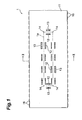
Fig. 1 is a plan view showing one embodiment of the wiring board of the present invention. -
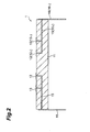
Fig. 2 is a cross sectional view taken along line II-II of the wiring board inFig. 1 . -
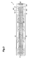
Fig. 3 is a view showing one example of a solid-state imaging element having the arrangement of terminal electrodes interchangeable in inputting and outputting depending on the frontside incident type or backside incident type. -
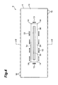
Fig. 4 is a plan view showing one embodiment of the solid-state imaging device of the present invention. -
Fig. 5 is a cross sectional view taken along line V-V of the solid-state imaging device inFig. 4 . -
Fig. 6 is a plan view showing another embodiment of the solid-state imaging device of the present invention. -
Fig. 7 is a cross sectional view taken along line VII-VII of the solid-state imaging device inFig. 6 . -
- 1: wiring board
- 2: solid-state imaging element
- 3: backside incident type solid-state imaging device
- 4: frontside incident type solid-state imaging device
- 11: substrate
- 12: first electrode pad
- 13: second electrode pad
- 14: positioning mark
- 15: internal wiring
- 16: external terminal
- 22, 35, 44: terminal electrodes
- 31: conductive bump
- 41: conductive wire
- 42: electrical insulating layer
- Findings of the present invention will be easily understood by considering a detailed description given below with reference to the attached views presented only for illustration. Then, a description will be given for embodiments of the present invention with reference to the attached views. Wherever possible, the same part is given the same reference symbol to omit a redundant description.
- The wiring board of the present embodiment will be described with reference to
Fig. 1 andFig. 2 .Fig. 1 is a plan view showing one embodiment of the wiring board of the present invention.Fig. 2 is a cross sectional view taken along line II-II of the wiring board inFig. 1 . The wiring board 1 is provided with a rectangular ceramicmulti-layered substrate 11 when viewed from above (the ceramic material is, for example, aluminum nitride).First electrode pads 12,second electrode pads 13 and positioning marks 14 are formed at predetermined positions on the front side thereof. Further, inside thesubstrate 11, aninternal wiring 15 is formed, and on the side face thereof, anexternal terminal 16 is formed. - A plurality of the
first electrode pads 12 are formed inside a to-be-arranged region 1a on the front side of thesubstrate 11. In this instance, the to-be-arranged region 1a is a region where a solid-state imaging element is arranged. The region is formed in a rectangular shape when viewed from above, extending to a longitudinal direction of thesubstrate 11 approximately at the center of thesubstrate 11. Thefirst electrode pads 12 are arranged in line along the peripheral part of the to-be-arranged region 1a which is rectangular in shape. It is noted that thefirst electrode pads 12 are to be bump-bonded to terminal electrodes of a backside incident type solid-state imaging element, and positions at which thefirst electrode pads 12 are formed correspond to those at which the thus arranged terminal electrodes of the backside incident type solid-state imaging element are formed. - A plurality of the
second electrode pads 13 are formed outside the to-be-arranged region 1a on the front side of thesubstrate 11. More specifically, these electrode pads are arranged in line outside the to-be-arranged region 1a so as to surround the rectangular to-be-arranged region 1a. Further, thesecond electrode pads 13 are formed in the same number as thefirst electrode pads 12. It is noted that thesecond electrode pads 13 are to be wire-bonded to the terminal electrodes of a frontside incident type solid-state imaging element and the positions at which thesecond electrode pads 13 are formed to correspond to those at which the thus arranged terminal electrodes of the frontside incident type solid-state imaging element are formed. Thefirst electrode pads 12 and thesecond electrode pads 13 are formed with a conductive material, for example, metal, by methods such as printing and sputtering. - The positioning marks 14 are formed to indicate a to-
be-arranged region 1a at which a solid-state imaging element is arranged. Specifically, the positioning marks 14 are formed at four positions between the thus arrangedfirst electrode pads 12 and the thus arrangedsecond electrode pads 13. Where a solid-state imaging device is arranged, the solid-state imaging element is fixed in such a manner that four corners of the element are respectively in alignment with the four positioning marks 14. The positioning marks 14 may be formed in the same manner as thefirst electrode pads 12 and thesecond electrode pads 13 by methods such as printing and sputtering. - The mutually corresponding
first electrode pads 12 andsecond electrode pads 13 are electrically connected byinternal wirings 15. Further, theinternal wirings 15 are electrically connected individually to a plurality ofexternal terminals 16 formed so as to extend from the side face of thesubstrate 11 to below. As a result, common input and output signals are to be transmitted to the thus correspondingfirst electrode pads 12 andsecond electrode pads 13 via theinternal wirings 15 and theexternal terminals 16. For example, where afirst electrode pad 121 is electrically connected to asecond electrode pad 131 and both of them are electrically connected to anexternal terminal 161, upon input of a vertical charge transfer pulse from theexternal terminal 161, the vertical charge transfer pulse is transmitted to both of thefirst electrode pad 121 and thesecond electrode pad 131 via theinternal wiring 151. - Therefore, the
first electrode pads 12 and thesecond electrode pads 13 electrically connected by theinternal wirings 15 are appropriately determined according to arrangements of the respective terminal electrodes of a frontside incident type solid-state imaging element and a backside incident type solid-state imaging element arranged on a wiring board. Where the arrangements of the respective terminal electrodes of the frontside incident type solid-state imaging element and the backside incident type solid-state imaging element arranged on a wiring board 1 are interchangeable in inputting and outputting depending on the frontside incident type or backside incident type, thefirst electrode pads 12 and thesecond electrode pads 13 which oppose each other behind the outer periphery of a rectangular to-be-arranged region 1a are connected by theinternal wirings 15. In this instance,adjacent electrode pads internal wirings 15. - In this instance, a description will be given for a frontside incident type solid-state imaging element and a backside incident type solid-state imaging element in which terminal electrodes are arranged so as to be interchangeable in inputting and outputting depending on the frontside incident type or backside incident type.
Fig. 3 is a view showing an example of the solid-state imaging element in which terminal electrodes are arranged so as to be interchangeable in inputting and outputting depending on the frontside incident type or backside incident type. The solid-state imaging element 2 is provided with aCCD 20, and theCCD 20 has a verticalcharge transfer portion 201 and horizontalcharge transfer portions charge transfer portion 201. Further,signal reading portions charge transfer portions signal reading portions center line 21 extending to a longitudinal direction of the solid-state imaging element 2. Thereby, an input/output interchangeable device which does not differ in the charge transfer direction (the solid line arrow indicates the transfer direction where the terminal electrodes are arranged on a wiring board from a backside S2, and the dotted line arrow indicates the transfer direction where they are arranged on the wiring board from a front side S1) and in the position at which signals are input and output, irrespective of whether the electrodes are arranged on the wiring board from the backside S2 or they are arranged on the wiring board from the front side S1, reversed around thecenter line 21. If theterminal electrodes 22 are arranged so as to be a line symmetry with respect to the center line extending to a width direction of the solid-state imaging element 2, the element can also be interchangeable in inputting and outputting depending on the frontside incident type or backside incident type. In this case, the horizontal charge transfer portion may be formed only on one end of the vertical charge transfer portion. - As described above, a plurality of the
first electrode pads 12 are formed inside the to-be-arranged region 1a and a plurality of thesecond electrode pads 13 are formed outside the to-be-arranged region 1a on the wiring board 1. Therefore, where a backside incident type solid-state imaging element is mounted, the terminal electrodes thereof can be electrically connected to thefirst electrode pads 12 by bump bonding. On the other hand, where a frontside incident type solid-state imaging element is mounted, the terminal electrodes can be electrically connected to thesecond electrode pads 13 by wire bonding. Further, since the mutually correspondingfirst electrode pads 12 andsecond electrode pads 13 are electrically connected, it is possible to transmit common input and output signals. Therefore, it is possible to provide the wiring board 1 high in general versatility and capable of mounting either the frontside incident type solid-state imaging element and the backside incident type solid-state imaging element. - Further, since the wiring board 1 is provided with positioning marks 14 indicating a to-
be-arranged region 1a, it is possible to arrange accurately a solid-state imaging element at the to-be-arranged region 1a on the basis of the positioning marks 14. - Then, a description will be given for one embodiment of the solid-state imaging device of the present invention with reference to
Fig. 4 andFig. 5 .Fig. 4 is a plan view showing one embodiment of the solid-state imaging device of the present invention.Fig. 5 is a cross sectional view taken along line V-V of the solid-state imaging device inFig. 4 . - A backside incident type solid-
state imaging device 3 is provided with a wiring board 1, a backside incident type solid-state imaging element 30 and aconductive bump 31. The backside incident type solid-state imaging device 3 is a device mounted on the wiring board of the above described one embodiment, the backside incident type solid-state imaging element having terminal electrodes arranged so as to be interchangeable in inputting and outputting depending on the frontside incident type or backside incident type as shown inFig. 3 . - The backside incident type solid-
state imaging element 30 is formed in a rectangular shape when viewed from above, corresponding in size to a to-be-arranged region 1a of the wiring board 1. The backside incident type solid-state imaging element 30 is constituted, for example, with a P+ layer of silicon and a P epi-layer formed thereon. ACCD 32 is formed at a part of the front side layer on the front side S1 thereof as a light detecting portion. TheCCD 32 is provided, for example, with a plurality of pixels of 1024 pixels × 128 pixels arranged in a two-dimensional manner. Further, theCCD 32 is provided with a verticalcharge transfer portion 321 and a horizontalcharge transfer portions Fig. 3 . - A backside incident type solid-
state imaging element 30 is also provided with a thinnedportion 33 formed which is thinned by etching a region of the backside S2 opposing theCCD 32. The thinnedportion 33 is formed having a flat light receiving face S3, the etched face of which is rectangular. And, the light receiving face S3 is formed so as to be approximately similar in size to theCCD 32. - The thickness of the backside incident type solid-
state imaging element 30 is approximately from 10 to 100 µm, for example, at the thinnedportion 33 and from 300 to 600 µm at an outer peripheral part of the thinnedportion 33. It is noted that the outerperipheral part 34 of the thinnedportion 33 is a part which is thicker than the thinnedportion 33 on the periphery of the thinnedportion 33 in the backside incident type solid-state imaging element 30. - A
terminal electrode 35 is formed at a peripheral part on the front side S1 of the backside incident type solid-state imaging element 30. Theterminal electrode 35 is arranged so as to be interchangeable in inputting and outputting depending on the frontside incident type or backside incident type as shown inFig. 3 . Further, theterminal electrode 35 is electrically connected to theCCD 32 by a wiring (not illustrated). Still further, the backside S2 of the backside incident type solid-state imaging element 30 is covered with an accumulation layer (not illustrated) for its entirety including the light receiving face S3. The accumulation layer has the same conductive type as that of the backside incident type solid-state imaging element 30 but higher in concentration of impurities than the backside incident type solid-state imaging element 30. - The backside incident type solid-
state imaging element 30 is implemented on a wiring board 1 by bump bonding. More specifically, the wiring board 1 is arranged so as to oppose the front side S1 of the backside incident type solid-state imaging element 30. In this case, the backside incident type solid-state imaging element 30 is adjusted for the position by the positioning marks 14 on the wiring board 1 and arranged at the to-be-arranged region 1a. Further, theterminal electrodes 35 formed on the front side S1 of the backside incident type solid-state imaging element 30 are connected to thefirst electrode pads 12 formed inside the to-be-arranged region 1a on the wiring board 1 individually via the conductive bumps 31. - The wiring board 1 is also provided with a package (not illustrated) which is opened at the center so as to cover the backside incident type solid-
state imaging element 30. A window member (not illustrated) is fitted into an opening part of the package. - As described above, since the wiring board 1 high in general versatility is used, it is possible to provide the backside incident type solid-
state imaging device 3 at a moderate price. - Then, a description will be given for another embodiment of the solid-state imaging device of the present invention with reference to
Fig. 6 andFig. 7 .Fig. 6 is a plan view showing another embodiment of the solid-state imaging device of the present invention.Fig. 7 is a cross sectional view taken along line VII-VII of the solid-state imaging device inFig. 6 . - A frontside incident type solid-
state imaging device 4 is provided with a wiring board 1, a frontside incident type solid-state imaging element 40, aconductive wire 41 and an electrical insulatinglayer 42. The frontside incident type solid-state imaging device 4 is provided with a frontside incident type solid-state imaging element being an interchangeable in inputting and outputting depending on the frontside incident type or backside incident type as shown inFig. 3 on the wiring board according to the above-described one enbodiment. - The frontside incident type solid-
state imaging element 40 differs from the backside incident type solid-state imaging element 30 in that no thinned portion is formed, and is identical in the other constitutions to the backside incident type solid-state imaging element 30. More specifically, the frontside incident type solid-state imaging element 40 is formed in a rectangular shape when viewed from above, corresponding in size to a to-be-arranged region 1a of the wiring board 1. ACCD 43 is formed at a part of the front side layer on the front side S1 thereof as a light detecting portion. TheCCD 43 is provided, for example, with a plurality of pixels of 1024 pixels × 128 pixels arranged in a two-dimensional manner. Further, theCCD 43 is provided with a verticalcharge transfer portion 431 and a horizontalcharge transfer portions 432, 433 as shown inFig. 3 . - The thickness of the frontside incident type solid-
state imaging element 40 is, for example, approximately from 300 to 600 µm.Terminal electrodes 44 are formed at a peripheral part on the front side S1 of the frontside incident type solid-state imaging element 40. Theterminal electrodes 44 are arranged so as to be interchangeable in inputting and outputting depending on the frontside incident type or of backside incident type as shown inFig. 3 . Further, theterminal electrodes 44 are electrically connected to theCCD 43 by a wiring (not illustrated). - The frontside incident type solid-
state imaging element 40 is mounted on the wiring board 1 by wire bonding. More specifically, the wiring board 1 is arranged so as to oppose the backside S2 of the frontside incident type solid-state imaging element 40. In this instance, the frontside incident type solid-state imaging element 40 is adjusted for the position by the positioning marks 14 on the wiring board 1 and arranged at the to-be-arranged region 1a. Further, an electrical insulatinglayer 42 is formed between the frontside incident type solid-state imaging element 40 and the wiring board 1. The electrical insulatinglayer 42 is formed in a rectangular shape when viewed from above, having such a size that covers the backside of the frontside incident type solid-state imaging element 40. Theterminal electrodes 44 formed on the front side S1 of the frontside incident type solid-state imaging element 40 are electrically connected to thesecond electrode pads 13 formed outside the to-be-arranged region 1a on the wiring board 1 via theconductive wires 41. - The wiring board 1 is also provided with a package (not illustrated) which is opened at the center so as to cover the frontside incident type solid-
state imaging element 40. A window member (not illustrated) is fitted into an opening part of the package. - As described above, since the wiring board 1 high in general versatility is used, it is possible to provide the frontside incident type solid-
state imaging device 4 at a moderate price. - Further, according to the frontside incident type solid-
state imaging device 4, since the frontside incident type solid-state imaging element 31 is mounted on the wiring board 1 via the electrical insulatinglayer 42, it is possible to electrically insulate the frontside incident type solid-state imaging element 40 from thesecond electrode pads 13 disposed on the wiring board 1. Thus, input and output signals can be transmitted to the frontside incident type solid-state imaging device 4 via the wiring board 1 without fail. - Still further, the solid-state imaging device of the present invention shall not be limited to the embodiments described above. The backside incident type solid-state imaging element mounted on the wiring board may include not only devices which are partially thinned but also those that are totally thinned in place of the former.
- The present invention is able to provide a wiring board high in general versatility capable of mounting either a frontside incident type solid-state imaging element and a backside incident type solid-state imaging element and a solid-state imaging device using the wiring board.
Claims (5)
- A wiring board having a to-be-arranged region at which a solid-state imaging element is arranged, including;
a plurality of first electrode pads formed inside the to-be-arranged region and
a plurality of second electrode pads formed outside the to-be-arranged region, each of which is electrically connected to each of the first electrode pads. - The wiring board according to claim 1 including;
positioning marks indicating the to-be-arranged region. - A solid-state imaging device in which a solid-state imaging element is arranged at a to-be-arranged region of a wiring board, wherein
the wiring board is provided with a plurality of first electrode pads formed inside the to-be-arranged region and a plurality of second electrode pads formed outside the to-be-arranged region, each of which is electrically connected to each of the first electrode pads;
the solid-state imaging element is provided with a light detecting portion disposed on a face opposing a light receiving face and a terminal electrode electrically connected to the light detecting portion;
the light detecting portion is provided with a vertical charge transfer portion, horizontal charge transfer portions disposed on both sides of the vertical charge transfer portion and a signal reading portion disposed at each of the horizontal charge transfer portions to read a signal from the horizontal charge transfer portion; and
the terminal electrodes are electrically connected to the first electrode pads by bump bonding. - A solid-state imaging device in which a solid-state imaging element is arranged at a to-be-arranged region on a wiring board, wherein
the wiring board is provided with a plurality of first electrode pads formed inside the to-be-arranged region and a plurality of second electrode pads formed outside the to-be-arranged region, each of which is electrically connected to each of the first electrode pads;
the solid-state imaging element is provided with a light detecting portion disposed on a light receiving face and a terminal electrode electrically connected to the light detecting portion;
the light detecting portion is provided with a vertical charge transfer portion, horizontal charge transfer portions disposed on both sides of the vertical charge transfer portion and a signal reading portion disposed at each of the horizontal charge transfer portions to read a signal from the horizontal charge transfer portion, and
the terminal electrodes are electrically connected to the second electrode pads by wire bonding. - The solid-state imaging device according to claim 4, wherein
an electrical insulating layer is disposed between the wiring board and the solid-state imaging element at the to-be-arranged region.
Applications Claiming Priority (2)
| Application Number | Priority Date | Filing Date | Title |
|---|---|---|---|
| JP2006190475A JP4451864B2 (en) | 2006-07-11 | 2006-07-11 | Wiring board and solid-state imaging device |
| PCT/JP2007/063494 WO2008007613A1 (en) | 2006-07-11 | 2007-07-05 | Wiring board and solid-state imaging device |
Publications (2)
| Publication Number | Publication Date |
|---|---|
| EP2043153A1 true EP2043153A1 (en) | 2009-04-01 |
| EP2043153A4 EP2043153A4 (en) | 2012-08-15 |
Family
ID=38923174
Family Applications (1)
| Application Number | Title | Priority Date | Filing Date |
|---|---|---|---|
| EP07768243A Withdrawn EP2043153A4 (en) | 2006-07-11 | 2007-07-05 | CONNECTION CHART AND SEMICONDUCTOR IMAGING DEVICE |
Country Status (6)
| Country | Link |
|---|---|
| US (1) | US20090243024A1 (en) |
| EP (1) | EP2043153A4 (en) |
| JP (1) | JP4451864B2 (en) |
| KR (1) | KR20090029189A (en) |
| CN (1) | CN101490844B (en) |
| WO (1) | WO2008007613A1 (en) |
Cited By (1)
| Publication number | Priority date | Publication date | Assignee | Title |
|---|---|---|---|---|
| US9583526B2 (en) | 2011-09-05 | 2017-02-28 | Hamamatsu Photonics K.K. | Solid-state image pickup element and solid-state image pickup element mounting structure |
Families Citing this family (2)
| Publication number | Priority date | Publication date | Assignee | Title |
|---|---|---|---|---|
| JP4421589B2 (en) * | 2006-10-10 | 2010-02-24 | 浜松ホトニクス株式会社 | Photodetector |
| JP4490406B2 (en) * | 2006-10-11 | 2010-06-23 | 浜松ホトニクス株式会社 | Solid-state imaging device |
Family Cites Families (20)
| Publication number | Priority date | Publication date | Assignee | Title |
|---|---|---|---|---|
| EP0478812A1 (en) | 1990-10-01 | 1992-04-08 | Societe Des Produits Nestle S.A. | Package for food product |
| JP2651323B2 (en) | 1992-07-22 | 1997-09-10 | 浜松ホトニクス株式会社 | Semiconductor energy detector |
| JP2888207B2 (en) | 1996-10-01 | 1999-05-10 | 日本電気株式会社 | Solid-state imaging device and driving method thereof |
| JP2897825B2 (en) * | 1996-12-20 | 1999-05-31 | 日本電気株式会社 | Solid-state imaging device |
| US5821532A (en) * | 1997-06-16 | 1998-10-13 | Eastman Kodak Company | Imager package substrate |
| US6501157B1 (en) * | 1998-04-15 | 2002-12-31 | Micron Technology, Inc. | Substrate for accepting wire bonded or flip-chip components |
| JP3494948B2 (en) * | 2000-03-22 | 2004-02-09 | シャープ株式会社 | Solid-state imaging device and method of manufacturing the same |
| US6384473B1 (en) * | 2000-05-16 | 2002-05-07 | Sandia Corporation | Microelectronic device package with an integral window |
| US6765801B1 (en) * | 2001-06-25 | 2004-07-20 | Amkor Technology, Inc. | Optical track drain package |
| DE10235332A1 (en) | 2002-08-01 | 2004-02-19 | Infineon Technologies Ag | Multiple layer switch support used in flip-chip technology comprises a semiconductor chip and/or a discrete component, a rewiring layer, an insulating layer with through-structures, and outer contact surfaces |
| US6885107B2 (en) * | 2002-08-29 | 2005-04-26 | Micron Technology, Inc. | Flip-chip image sensor packages and methods of fabrication |
| JP4195594B2 (en) | 2002-09-06 | 2008-12-10 | ジーイー・メディカル・システムズ・グローバル・テクノロジー・カンパニー・エルエルシー | Vector switching method for offset correction and X-ray CT apparatus |
| WO2004060034A1 (en) * | 2002-12-24 | 2004-07-15 | Matsushita Electric Industrial Co., Ltd. | Electronic component-built-in module |
| JP4364514B2 (en) * | 2003-01-08 | 2009-11-18 | 浜松ホトニクス株式会社 | Wiring board and radiation detector using the same |
| JP2004219318A (en) * | 2003-01-16 | 2004-08-05 | Hamamatsu Photonics Kk | Radiation detector |
| SG143932A1 (en) * | 2003-05-30 | 2008-07-29 | Micron Technology Inc | Packaged microelectronic devices and methods of packaging microelectronic devices |
| JP4499386B2 (en) * | 2003-07-29 | 2010-07-07 | 浜松ホトニクス株式会社 | Manufacturing method of back-illuminated photodetector |
| JP4494745B2 (en) * | 2003-09-25 | 2010-06-30 | 浜松ホトニクス株式会社 | Semiconductor device |
| JP4606063B2 (en) * | 2004-05-14 | 2011-01-05 | パナソニック株式会社 | Optical device and manufacturing method thereof |
| US7276393B2 (en) * | 2004-08-26 | 2007-10-02 | Micron Technology, Inc. | Microelectronic imaging units and methods of manufacturing microelectronic imaging units |
-
2006
- 2006-07-11 JP JP2006190475A patent/JP4451864B2/en not_active Expired - Lifetime
-
2007
- 2007-07-05 WO PCT/JP2007/063494 patent/WO2008007613A1/en not_active Ceased
- 2007-07-05 US US12/373,106 patent/US20090243024A1/en not_active Abandoned
- 2007-07-05 CN CN2007800263397A patent/CN101490844B/en active Active
- 2007-07-05 KR KR1020087027765A patent/KR20090029189A/en not_active Ceased
- 2007-07-05 EP EP07768243A patent/EP2043153A4/en not_active Withdrawn
Cited By (1)
| Publication number | Priority date | Publication date | Assignee | Title |
|---|---|---|---|---|
| US9583526B2 (en) | 2011-09-05 | 2017-02-28 | Hamamatsu Photonics K.K. | Solid-state image pickup element and solid-state image pickup element mounting structure |
Also Published As
| Publication number | Publication date |
|---|---|
| EP2043153A4 (en) | 2012-08-15 |
| WO2008007613A1 (en) | 2008-01-17 |
| JP4451864B2 (en) | 2010-04-14 |
| CN101490844B (en) | 2011-02-16 |
| JP2008021724A (en) | 2008-01-31 |
| KR20090029189A (en) | 2009-03-20 |
| CN101490844A (en) | 2009-07-22 |
| US20090243024A1 (en) | 2009-10-01 |
Similar Documents
| Publication | Publication Date | Title |
|---|---|---|
| EP2077581B1 (en) | Solid-state imaging device | |
| US7515203B2 (en) | Image capture apparatus | |
| CN103782388B (en) | Solid-state imager and the installation constitution of solid-state imager | |
| KR102877798B1 (en) | Semiconductor package | |
| TWI302742B (en) | Solid-state image sensing device | |
| JP4601331B2 (en) | Imaging device and imaging module | |
| US20090243024A1 (en) | Wiring board and solid-state imaging device | |
| JP4720120B2 (en) | Semiconductor image sensor module | |
| EP2963686B1 (en) | Semiconductor photodetection device | |
| JP4714502B2 (en) | Solid-state imaging device | |
| US20080217515A1 (en) | Illuminance detection apparatus and sensor module | |
| CN101536489B (en) | Solid-state imaging device and electronic equipment | |
| EP4235769A1 (en) | Imaging device, electronic apparatus, and method for manufacturing imaging device | |
| JP4822624B2 (en) | Package for pressure detection device | |
| US7579579B2 (en) | Integrated photoreceptor circuit and optoelectronic component including the same with electric contact pads arranged solely on side of the processing area which is juxtaposed with the photosensitive area | |
| JP2009111130A (en) | Imaging apparatus and manufacturing method thereof | |
| US20070090284A1 (en) | Image sensor package structure | |
| JP5908218B2 (en) | Optical sensor and optical sensor manufacturing method | |
| JP4753926B2 (en) | Pressure detector and pressure detector assembly | |
| JP4925522B2 (en) | Package for pressure detection device | |
| JP4794072B2 (en) | Package for pressure detection device | |
| JP4557676B2 (en) | Mounting structure of semiconductor device | |
| JP2004208086A (en) | Imaging device | |
| JP2004340575A (en) | Package for pressure detector | |
| JPH10116973A (en) | Solid-state imaging device |
Legal Events
| Date | Code | Title | Description |
|---|---|---|---|
| PUAI | Public reference made under article 153(3) epc to a published international application that has entered the european phase |
Free format text: ORIGINAL CODE: 0009012 |
|
| 17P | Request for examination filed |
Effective date: 20090119 |
|
| AK | Designated contracting states |
Kind code of ref document: A1 Designated state(s): AT BE BG CH CY CZ DE DK EE ES FI FR GB GR HU IE IS IT LI LT LU LV MC MT NL PL PT RO SE SI SK TR |
|
| AX | Request for extension of the european patent |
Extension state: AL BA HR MK RS |
|
| DAX | Request for extension of the european patent (deleted) | ||
| RBV | Designated contracting states (corrected) |
Designated state(s): DE FR GB |
|
| A4 | Supplementary search report drawn up and despatched |
Effective date: 20120716 |
|
| RIC1 | Information provided on ipc code assigned before grant |
Ipc: H01L 27/146 20060101AFI20120710BHEP Ipc: H05K 1/11 20060101ALI20120710BHEP Ipc: H05K 1/02 20060101ALI20120710BHEP |
|
| 17Q | First examination report despatched |
Effective date: 20120727 |
|
| STAA | Information on the status of an ep patent application or granted ep patent |
Free format text: STATUS: THE APPLICATION IS DEEMED TO BE WITHDRAWN |
|
| 18D | Application deemed to be withdrawn |
Effective date: 20150630 |