EP2040362B1 - Power supply apparatus - Google Patents
Power supply apparatus Download PDFInfo
- Publication number
- EP2040362B1 EP2040362B1 EP07745467.6A EP07745467A EP2040362B1 EP 2040362 B1 EP2040362 B1 EP 2040362B1 EP 07745467 A EP07745467 A EP 07745467A EP 2040362 B1 EP2040362 B1 EP 2040362B1
- Authority
- EP
- European Patent Office
- Prior art keywords
- voltage
- converter
- power supply
- time
- power source
- Prior art date
- Legal status (The legal status is an assumption and is not a legal conclusion. Google has not performed a legal analysis and makes no representation as to the accuracy of the status listed.)
- Active
Links
- 230000002457 bidirectional effect Effects 0.000 claims description 17
- 238000005070 sampling Methods 0.000 claims 1
- 238000010586 diagram Methods 0.000 description 71
- 239000003990 capacitor Substances 0.000 description 54
- 239000007858 starting material Substances 0.000 description 36
- 230000008929 regeneration Effects 0.000 description 29
- 238000011069 regeneration method Methods 0.000 description 29
- 230000007423 decrease Effects 0.000 description 25
- 230000003247 decreasing effect Effects 0.000 description 9
- 230000007274 generation of a signal involved in cell-cell signaling Effects 0.000 description 9
- 238000009499 grossing Methods 0.000 description 8
- 238000007599 discharging Methods 0.000 description 6
- 230000007774 longterm Effects 0.000 description 6
- 238000000034 method Methods 0.000 description 4
- 230000001172 regenerating effect Effects 0.000 description 4
- 230000006866 deterioration Effects 0.000 description 3
- 238000005516 engineering process Methods 0.000 description 2
- 230000007613 environmental effect Effects 0.000 description 2
- 238000002360 preparation method Methods 0.000 description 2
- 238000011084 recovery Methods 0.000 description 2
- 230000000717 retained effect Effects 0.000 description 2
- 230000003213 activating effect Effects 0.000 description 1
- 238000006243 chemical reaction Methods 0.000 description 1
- 230000002950 deficient Effects 0.000 description 1
- 230000002542 deteriorative effect Effects 0.000 description 1
- 239000000446 fuel Substances 0.000 description 1
- 230000010355 oscillation Effects 0.000 description 1
- 230000000630 rising effect Effects 0.000 description 1
- 230000000087 stabilizing effect Effects 0.000 description 1
- 230000002123 temporal effect Effects 0.000 description 1
Images


Classifications
-
- H—ELECTRICITY
- H02—GENERATION; CONVERSION OR DISTRIBUTION OF ELECTRIC POWER
- H02J—CIRCUIT ARRANGEMENTS OR SYSTEMS FOR SUPPLYING OR DISTRIBUTING ELECTRIC POWER; SYSTEMS FOR STORING ELECTRIC ENERGY
- H02J9/00—Circuit arrangements for emergency or stand-by power supply, e.g. for emergency lighting
- H02J9/04—Circuit arrangements for emergency or stand-by power supply, e.g. for emergency lighting in which the distribution system is disconnected from the normal source and connected to a standby source
- H02J9/06—Circuit arrangements for emergency or stand-by power supply, e.g. for emergency lighting in which the distribution system is disconnected from the normal source and connected to a standby source with automatic change-over, e.g. UPS systems
- H02J9/061—Circuit arrangements for emergency or stand-by power supply, e.g. for emergency lighting in which the distribution system is disconnected from the normal source and connected to a standby source with automatic change-over, e.g. UPS systems for DC powered loads
-
- G—PHYSICS
- G11—INFORMATION STORAGE
- G11C—STATIC STORES
- G11C27/00—Electric analogue stores, e.g. for storing instantaneous values
- G11C27/02—Sample-and-hold arrangements
- G11C27/024—Sample-and-hold arrangements using a capacitive memory element
-
- H—ELECTRICITY
- H02—GENERATION; CONVERSION OR DISTRIBUTION OF ELECTRIC POWER
- H02M—APPARATUS FOR CONVERSION BETWEEN AC AND AC, BETWEEN AC AND DC, OR BETWEEN DC AND DC, AND FOR USE WITH MAINS OR SIMILAR POWER SUPPLY SYSTEMS; CONVERSION OF DC OR AC INPUT POWER INTO SURGE OUTPUT POWER; CONTROL OR REGULATION THEREOF
- H02M3/00—Conversion of dc power input into dc power output
- H02M3/02—Conversion of dc power input into dc power output without intermediate conversion into ac
- H02M3/04—Conversion of dc power input into dc power output without intermediate conversion into ac by static converters
- H02M3/10—Conversion of dc power input into dc power output without intermediate conversion into ac by static converters using discharge tubes with control electrode or semiconductor devices with control electrode
- H02M3/145—Conversion of dc power input into dc power output without intermediate conversion into ac by static converters using discharge tubes with control electrode or semiconductor devices with control electrode using devices of a triode or transistor type requiring continuous application of a control signal
- H02M3/155—Conversion of dc power input into dc power output without intermediate conversion into ac by static converters using discharge tubes with control electrode or semiconductor devices with control electrode using devices of a triode or transistor type requiring continuous application of a control signal using semiconductor devices only
-
- H—ELECTRICITY
- H02—GENERATION; CONVERSION OR DISTRIBUTION OF ELECTRIC POWER
- H02J—CIRCUIT ARRANGEMENTS OR SYSTEMS FOR SUPPLYING OR DISTRIBUTING ELECTRIC POWER; SYSTEMS FOR STORING ELECTRIC ENERGY
- H02J7/00—Circuit arrangements for charging or depolarising batteries or for supplying loads from batteries
- H02J7/34—Parallel operation in networks using both storage and other dc sources, e.g. providing buffering
- H02J7/345—Parallel operation in networks using both storage and other dc sources, e.g. providing buffering using capacitors as storage or buffering devices
-
- H—ELECTRICITY
- H02—GENERATION; CONVERSION OR DISTRIBUTION OF ELECTRIC POWER
- H02M—APPARATUS FOR CONVERSION BETWEEN AC AND AC, BETWEEN AC AND DC, OR BETWEEN DC AND DC, AND FOR USE WITH MAINS OR SIMILAR POWER SUPPLY SYSTEMS; CONVERSION OF DC OR AC INPUT POWER INTO SURGE OUTPUT POWER; CONTROL OR REGULATION THEREOF
- H02M1/00—Details of apparatus for conversion
- H02M1/0003—Details of control, feedback or regulation circuits
- H02M1/0016—Control circuits providing compensation of output voltage deviations using feedforward of disturbance parameters
- H02M1/0022—Control circuits providing compensation of output voltage deviations using feedforward of disturbance parameters the disturbance parameters being input voltage fluctuations
-
- H—ELECTRICITY
- H02—GENERATION; CONVERSION OR DISTRIBUTION OF ELECTRIC POWER
- H02M—APPARATUS FOR CONVERSION BETWEEN AC AND AC, BETWEEN AC AND DC, OR BETWEEN DC AND DC, AND FOR USE WITH MAINS OR SIMILAR POWER SUPPLY SYSTEMS; CONVERSION OF DC OR AC INPUT POWER INTO SURGE OUTPUT POWER; CONTROL OR REGULATION THEREOF
- H02M1/00—Details of apparatus for conversion
- H02M1/0003—Details of control, feedback or regulation circuits
- H02M1/0025—Arrangements for modifying reference values, feedback values or error values in the control loop of a converter
Definitions
- the present invention relates to a power supply unit compensating voltage fluctuation of a power source.
- stop idling In recent years, to protect the earth environment from the aspect of improving fuel efficiency especially in automobiles, technologies have been developed such as stop idling, electromotive power steering, electromotive turbocharger, and brake regeneration.
- stop idling, electromotive power steering, and electromotive turbocharger consume a large amount of current on the order of 100 amperes to activate a starter, steering motor, and turbine drive motor, respectively, thus causing a voltage drop in a power source composed of such as a battery and power generator.
- a large voltage drop prevents a load powered from the power source from operating satisfactorily.
- brake regeneration generates a regenerative current on the order of a maximum of 100 amperes, depending on the vehicle speed, thereby increasing the voltage of the power source. Directly supplying such voltage causes supply voltage to the load to increase, possibly preventing normal operation.
- a voltage drop protection circuit is provided between the battery and auxiliaries.
- the voltage drop protection circuit may use either of the following method. That is, one includes a capacitor as an auxiliary power supply as described in Patent Document 1, and the voltage is compensated by supplying auxiliaries with power from the capacitor when the battery voltage drops. The other does not include an auxiliary power supply, but the voltage is compensated by raising the voltage of the battery to supply to auxiliaries when the battery voltage drops.
- the voltage drop protection circuit requires a DC/DC converter that converts voltage of a capacitor and/or battery to that required for operation of auxiliaries.
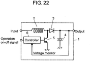
- a description is made for a concrete example of a voltage drop protection circuit including a capacitor as an auxiliary power supply, using Fig. 22 .
- voltage drop protection circuit 1 includes a DC/DC converter circuit configuration, where its input is connected to the output through coil 2 and diode 3.
- the connecting point of the cathode of diode 3 with the output is connected to the ground through capacitor 4.
- the connecting points of coil 2 with diode 3 are connected to the ground through transistor 5, and the base of transistor 5 is connected to the output from controller 6.
- Controller 6 monitors output voltage of voltage drop protection circuit 1 to on-off control transistor 5. Operation of controller 6 is controlled according to an on-off signal from the outside.
- transistor 5 is on-off controlled by controller 6 operating according to an operation on-off signal and charges capacitor 4 with voltage increased by means of coil 2. Additionally, controller 6 monitors output voltage of voltage drop protection circuit 1 to maintain the voltage at a predetermined output set value. Consequently, even in a low-voltage state of the battery, the output voltage of voltage drop protection circuit 1 can be controlled so as not to decrease.
- controller 6 monitors output voltage of voltage drop protection circuit 1 to maintain the voltage at a predetermined output set value. Consequently, even in a low-voltage state of the battery, the output voltage of voltage drop protection circuit 1 can be controlled so as not to decrease.
- the above is an example of a power supply unit compensating a voltage drop of a power source.
- Patent Document 1 compensates a voltage drop of a battery. Meanwhile, output voltage of voltage drop protection circuit 1 may be suppressed by storing power in brake regeneration to capacitor 4, for example.
- the problem lies in the fact that the voltage output set value of controller 6 is constant. That is, a battery or the like as a power source produces voltage fluctuation relatively small (concretely, a range between approximately 12 V and 14 V) over a long duration according to an environment change such as fluctuation in ambient temperature and/or deterioration. For this reason, the output set value of controller 6 is fixed to a value (e.g. 11 V) lower than the lowest value (12 V) in a long-term voltage fluctuation range of the battery in order to output power from the battery preferentially in normal times, during which a temporary voltage fluctuation of the battery does not occur.
- a value e.g. 11 V
- controller 6 When performing regeneration by braking, the voltage of the power source temporarily increases as well, and thus controller 6 operates so as to charge capacitor 4 when a certain predetermined voltage (e.g. 14.5 V) is exceeded. At this moment, if the voltage of such as a battery before regeneration is 14 V, the voltage fluctuation is small, however if the battery voltage is 12 V, the supply voltage to the load suddenly increases to 14.5 V, which can possibly affect the load in the same way as the above.
- a certain predetermined voltage e.g. 14.5 V
- Patent Document 1 Japanese Patent Unexamined Publication No. 2005-112250
- European Patent Application EP 1209549 A2 discloses a power supply with the features of the preamble of claim 1.
- Japanese Patent Application JP H04 251522 A discloses an auxiliary power supply compensating load voltage fluctuations.
- the present invention provides a power supply unit in which the difference is always small between the voltage of a power source in normal times and the output voltage of a DC/DC converter when the voltage of the power source fluctuates.
- a power supply unit of the present invention includes a sample-and-hold circuit that samples voltage corresponding to the voltage supplied from a power source to a load according to sample timing signal 27 and holds the voltage as an output set value of the DC/DC converter.
- the power supply unit controls the output voltage of the DC/DC converter so as to be the output set value.
- the output set value of a DC/DC converter is updated to a value corresponding to the voltage of the power source immediately before voltage fluctuation, and thus even if the voltage of the power source in normal times fluctuates due to environmental influence, the output voltage of the DC/DC converter is controlled according to the fluctuation. This enables the difference is always small between the voltage of a power source in normal times and the output voltage of a DC/DC converter when the voltage of the power source fluctuates, thereby keeping the load stably operated.
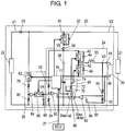
- Fig. 1 is a block circuit diagram of a power supply unit according to the first embodiment of the present invention.
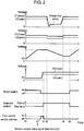
- Fig. 2 is a timing diagram showing the operation of the power supply unit according to the first embodiment of the present invention.
- Fig. 2 includes time-lapse change of voltage V1 of power source 22, time-lapse change of voltage V2 supplied to load 21, time-lapse change of voltage V3 of auxiliary power supply 30, time-lapse change of voltage V4 of capacitor 88 for sample and hold, an on-off timing diagram of third switch 26, a switching timing diagram of selector switch 66, and an on-off timing diagram of first and second sample switches 82, 86.
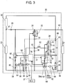
- Fig. 3 is a block circuit diagram of a power supply unit with another structure, according to the first embodiment of the present invention.
- power supply unit 20 supplies load 21 with power, where they are electrically connected to each other.
- Power supply unit 20 comprises power source 22 including a battery and generator, selection switch 23, DC/DC converter 24, third switch 26, sample-and-hold circuit 28, and auxiliary power supply 30 including a capacitor capable of charging and discharging.
- selection switch 23 switches between output from power source 22 and output from DC/DC converter 24 as a power source supplying load 21 with power.
- selection switch 23 is composed of a diode to automatically change so as to supply load 21 with power from auxiliary power supply 30 when voltage V1 of power source 22 drops. This prevents a current output from auxiliary power supply 30 through DC/DC converter 24 from flowing back to power source 22 when voltage V1 temporarily drops.
- DC/DC converter 24 is a bidirectional converter capable of charging and discharging auxiliary power supply 30 with a single circuit.
- third switch 26 has rectifier element 32 in parallel therewith and can be on-off controlled externally, and an FET is used as third switch in the first embodiment.
- rectifier element 32 works as a body diode of the FET.
- a capacitor used for auxiliary power supply 30 is an electric double-layer capacitor that has excellent rapid charge-discharge characteristic and large capacity. With these structure, DC/DC converter 24 obtains output voltage from power source 22 or auxiliary power supply 30.
- third switch 26 One end of third switch 26 is connected to first Input/Output (I/O) terminal 34 of DC/DC converter 24, and the other end is connected to the connecting point of selection switch 23 and load 21. Consequently, power source 22 is connected to DC/DC converter 24 through third switch 26.
- rectifier element 32 is connected so that first I/O terminal 34 side is an anode.
- first I/O terminal 34 has smoothing capacitor 38 connected thereto between terminal 34 and ground 36 for smoothing output in step-up operation.
- the capacitance of the electric double-layer capacitor of auxiliary power supply 30 is larger than a capacitance of smoothing capacitor 38.
- Both ends of smoothing capacitor 38 have two switches (first switch 40, second switch 42) series-connected thereto.
- first switch 40 and second switch 42 can be externally controlled so as to alternately repeat on-off operation.
- FETs are used as first and second switches 40, 42 in the first embodiment, as well as third switch 26. Therefore, body diodes 44, 46 are formed as shown by the broken lines in the wiring of Fig. 1 .
- First switch 40 is connected to a positive electrode side of smoothing capacitor 38 so that voltage between the positive and negative electrodes of second I/O terminal 48 of DC/DC converter 24 becomes higher as on-time of first switch 40 becomes longer.
- first switch 40 with second switch 42 is connected to one end of coil 50 (i.e. inductance element).
- the other end of coil 50 is connected to the positive electrode of second I/O terminal 48 giving and receiving power to and from auxiliary power supply 30.
- a smoothing capacitor for smoothing output is not provided in the first embodiment, however it may be provided between the positive and negative electrodes of second I/O terminal 48.
- first error amplifier 56 To detect voltage V5 at first I/O terminal 34, two resistors 52, 54 for detecting voltage V5 are series-connected between first I/O terminal 34 and ground 36. With these resistors, voltage at the connecting point of resistors 52, 54 for detecting voltage V5 is detected as voltage proportional to voltage V5. Therefore, by connecting the connecting point to one input terminal of first error amplifier 56 and connecting an output set value determined by sample-and-hold circuit 28 to the other input terminal, first error amplifier 56 outputs an error between them to make voltage V5 equivalent to the output set value when auxiliary power supply 30 discharges (i.e. in step-up operation of DC/DC converter 24 in the first embodiment). The detailed structure of sample-and-hold circuit 28 is described later.
- two resistors 58, 60 for detecting voltage V3 are series-connected between the positive electrode of second I/O terminal 48 and the negative electrode of auxiliary power supply 30.
- the voltage at the connecting point of resistors 58, 60 for detecting voltage V3 is detected as voltage proportional to voltage V3. Therefore, by connecting the connecting point to one input terminal of second error amplifier 62 and connecting set voltage source 64 to the other input terminal, second error amplifier 62 outputs an error between them to make voltage V3 corresponding to the output set value when charging auxiliary power supply 30 (i.e. in step-down operation of DC/DC converter 24 in the first embodiment).
- first error amplifier 56 and that of second error amplifier 62 are connected to selector switch 66 for selecting either one of them.
- This selector switch 66 switches between step-up and step-down operation. That is, when selector switch 66 selects the output of first error amplifier 56, step-up operation from auxiliary power supply 30 to load 21 is to be performed; when selector switch 66 selects the output from second error amplifier 62, step-down operation from power source 22 to auxiliary power supply 30 is to be performed.
- Switching signal generation circuit 68 compares a signal having been input with output from oscillation circuit 70 using comparator 72, generates a pulse signal for turning on and off first switch 40 and second switch 42, divides an input into two, and inputs one of them to inverting circuit 74 to generate on and off signals mutually inverted. These signals are separately input to first switch 40 and second switch 42 to perform voltage conversion (i.e. step-up and step-down of DC/DC converter 24).
- switching control of selector switch 66, operation control of switching signal generation circuit 68, on-off control of third switch 26, and operation control of sample-and-hold circuit 28 are performed by control circuit 76. Of these, the operation of switching signal generation circuit 68 is controlled by receiving switching start-up signal 77 from control circuit 76.
- Sample-and-hold circuit 28 has a function to sample voltage corresponding to voltage V2 currently supplied from power source 22 to load 21 according to sample timing signal 27 delivered from an external unit, e.g. from an engine ECU, and to hold it as an output set value of DC/DC converter 24.
- resistors 78, 80 for detecting voltage V2 are connected between the positive electrode of load 21 and ground 36. With these resistors, voltage at the connecting point of resistors 78, 80 for detecting voltage V2 is detected as voltage proportional to V2.
- resistors 78, 80 for detecting voltage V2 are directly connected between the positive electrode of load 21 and ground 36, a current from power source 22 results in always flowing into resistors 78, 80 for detecting voltage V2, causing a great loss.
- first sample switch 82 is series-connected so that resistors 78, 80 for detecting voltage V2 function only when sample and hold are required.
- the connecting point of resistors 78, 80 for detecting voltage V2 is connected to capacitor 88 for sample and hold through voltage follower 84 and second sample switch 86.
- second sample switch 86 is turned off to hold voltage corresponding to voltage V2. Therefore, first and second sample switches 82, 86 are controlled by control circuit 76 so as to be simultaneously turned on only during sample and hold operation.
- the voltage output copied to capacitor 88 for sample and hold is input to first error amplifier 56 as an output set value of DC/DC converter 24.
- voltage follower 84 is used as a circuit configuration capable of decreasing voltage V4 to voltage corresponding to voltage V2. This voltage follower 84 allows electric charge of capacitor 88 for sample and hold to automatically escape through the ground terminal (not shown) of voltage follower 84 until voltage V4 decreases to voltage corresponding to voltage V2.
- the output set value of DC/DC converter 24 is determined so that, when voltage V1 of power source 22 drops, voltage supplied from auxiliary power supply 30 to load 21 is lower than the voltage supplied from power source 22 to load 21 in normal times. This reason is described later in the description for operation.
- resistors 78, 80 for detecting voltage V2 having resistances with which the voltage decreases at a constant rate have only to be used, for example.
- resistances with which the voltage decreases by approximately 10% is selected.
- DC/DC converter 24 performs control so that voltage V5 of first I/O terminal 34 becomes an output set value.
- Rectifier element 32 is connected between first I/O terminal 34 and load 21, thereby causing a voltage drop. Consequently, simply using a resistance with which the voltage decreases at a constant rate results in an excessively low output voltage from auxiliary power supply 30 by the voltage drop. Accordingly, the output set value of DC/DC converter 24 is preliminarily raised by voltage corresponding to a voltage drop at rectifier element 32.
- the resistances of resistors 78, 80 for detecting voltage V2 are set so that the voltage is eventually decreased at a constant rate (approximately 10%) while being increased by a voltage drop at rectifier element 32.
- an output set value of DC/DC converter 24 is determined by setting resistances of resistors 78, 80 for detecting voltage V2.
- an output set value may be determined by setting resistances of resistors 52, 54 for detecting voltage V5 in the same way as the above.
- voltage V1 of power source 22 is a certain constant value when power supply unit 20 starts up (time t0) as shown in Fig. 2 .
- voltage V1 is shown by a solid line V1(max) and a dotted line V1(min), showing a fluctuation range of power source 22 according to a change in ambient temperature or a deterioration, where the maximum value of voltage V1 is indicated by a solid line and the minimum by a dotted line.
- control circuit 76 turns on third switch 26 and sets selector switch 66 to the step-down position as shown in Fig. 2 . Meanwhile, since sample timing signal 27 from the ECU is off immediately after start-up, first and second sample switches 82, 86 remain off as shown in Fig. 2 .
- control circuit 76 delivers switching start-up signal 77 to drive switching signal generation circuit 68. Since selector switch 66 has been switched to the step-down position, DC/DC converter 24 charges auxiliary power supply 30 with power from power source 22. In this case, DC/DC converter 24 performs control for step-down operation so that voltage V3 corresponds to the voltage of set voltage source 64. Consequently, as shown in Fig. 2 , voltage V3 increases as time elapses.
- Starter operation is performed when a driver changes step from a brake pedal to a gas pedal during a stop, for example.
- the ECU transmits sample timing signal 27 (pulse signal) to control circuit 76 simultaneously with detecting a step change of the pedals.
- the starter has not been operated yet.
- control circuit 76 When control circuit 76 receives sample timing signal 27 at time t1, control circuit 76 immediately turns off third switch 26 and at the same time turns on first and second sample switches 82, 86 as shown in Fig. 2 . Consequently, by turning off third switch 26, control circuit 76 cuts power input from power source 22, at first. Meanwhile, by turning on first and second sample switches 82, 86, control circuit 76 copies voltage V2 currently supplied to load 21 to capacitor 88 for sample and hold as a voltage proportional to voltage V2 resistively divided with resistors 78, 80 for detecting voltage V2. Time for charging is required to reach a level at which voltage V4 of capacitor 88 for sample and hold reaches a voltage corresponding to voltage V2. Under the circumstances, as shown in Fig. 2 , first and second sample switches 82, 86 are kept on until time t2 (preliminarily determined) when voltage V4 is stabilized with sufficient charge accumulated.
- control circuit 76 turns off first and second sample switches 82, 86 as shown in Fig. 2 to hold voltage V4 remaining constant and simultaneously changes selector switch 66 to the step-up position. With this operation, whenever the starter is driven to drop voltage V1, auxiliary power supply 30 is ready to supply load 21 with power.
- the output voltage of DC/DC converter 24 is controlled so as to be an output set value held at time t2. Consequently, after time t3, voltage V2 can be voltage nearly the same as that before the starter is operated. Consequently, if power source 22 provides a high voltage value as shown by the solid line of voltage V2 in Fig. 2 , a voltage close to the voltage value is supplied to load 21. Meanwhile, if power source 22 provides a low voltage value as shown by the dotted line of voltage V2, a voltage close to the voltage value is supplied to load 21. Accordingly, by performing variance control on the output voltage of DC/DC converter 24 so that voltage V4 sampled by sample-and-hold circuit 28 becomes the output set value, the output voltage can follow long-term voltage fluctuation of power source 22. This reduces the possibility that the fluctuation in the difference between the voltage from power source 22 and that the voltage from auxiliary power supply 30 influences the operation of load 21 depending on conditions of power source 22, as seen conventionally.
- auxiliary power supply 30 is slightly lower than the voltage from power source 22.
- the embodiment is structured so that voltage lower than that supplied from power source 22 to load 21 is preliminarily held as an output set value.
- the reason for such a structure is to avoid the following possibility. That is, if voltage from auxiliary power supply 30 is higher than the voltage from power source 22, power is supplied from auxiliary power supply 30 to load 21 even if voltage V1 is not low, and the starter has not been operated yet from time t2 to time t3. This causes insufficient power supplied from auxiliary power supply 30 when actually required. Setting the resistances of resistors 78, 80 for detecting voltage V2 for the above purpose is the same as described in the structure of sample-and-hold circuit 28.
- control circuit 76 turns on third switch 26 at time t5 and changes selector switch 66 to the step-down position as shown in Fig. 2 . Since this state is the same as that at time t0, the operation same as that from time t0 to time t1 charges auxiliary power supply 30. Consequently, voltage V3 increases after time t5 as shown in Fig. 2 , and when fully charged, operation is performed so as to maintain the voltage.
- sample timing signal 27 is received again in this state to turn on first and second sample switches 82, 86, voltage V4 is updated to voltage corresponding to voltage V2 at the time, where if voltage V4 is lower than voltage corresponding to voltage V2, capacitor 88 for sample and hold is charged until voltage corresponding to voltage V2 is reached. Meanwhile, if voltage V4 is higher than voltage corresponding to voltage V2, discharge is made from capacitor 88 for sample and hold to the ground of voltage follower 84 to a level at which voltage corresponding to voltage V2 is reached as described in the structure of sample-and-hold circuit 28. In this way, sample-and-hold circuit 28 with the structure of the first embodiment enables voltage V4 to be automatically updated to a voltage corresponding to voltage V2 only by turning on first and second sample switches 82, 86.
- the above-described structure and operation provide power supply unit 20 in which the difference is always small between voltage of power source 22 in normal times and output voltage of DC/DC converter 24 when the voltage of power source 22 drops.
- DC/DC converter 24 step ups the voltage of auxiliary power supply 30 to supply load 21 with power.
- the following structure provides the same advantages. That is, a well-known step-down type converter, or step-up and step-down type converters may be used as DC/DC converter 24 that steps down the high voltage of auxiliary power supply 30 to supply power from auxiliary power supply 30 to load 21.
- the structure is shown in which power source 22 and auxiliary power supply 30 are connected in parallel through DC/DC converter 24.
- power source 22 may be series-connected to auxiliary power supply 30 as shown in Fig. 3 .
- the other circuit configuration is the same as that of Fig. 1 except that the step-up and step-down positions of selector switch 66 are inverted.
- the voltage to charge auxiliary power supply 30 needs to be higher than voltage V1 of power source 22 , and thus DC/DC converter 24 is to perform step-up operation when charging. Consequently, during a voltage drop period of power source 22, high voltage V3 of auxiliary power supply 30 is stepped down and supplied to load 2.
- step-up and step-down operation of DC/DC converter 24 is to be inverted from the operation of Fig. 1 , and thus the step-up and step-down positions of the selector switch in Fig. 2 need to be inverted.
- Temporal operation other than this is the same as that of Fig. 2 .
- the voltage drop characteristic of voltage V3 during the voltage drop period (time t3 to t4) of voltage V3 in Fig. 2 is not linear, but has a characteristic given by being combined with fluctuation of voltage V1 during the period t3 to t4 in Fig. 2 . In other words, it is a characteristic (not shown) in which the voltage is decreasing like the time-lapse change of voltage V3 in Fig. 2 as a whole while including short-term voltage fluctuation of V1.
- auxiliary power supply 30 even after auxiliary power supply 30 is fully charged, for example, DC/DC converter 24 continues to be operated to maintain the fully charged voltage.
- the electric double-layer capacitor with a large capacitance used in auxiliary power supply 30 prevents the voltage from rapidly decreasing even if DC/DC converter 24 is stopped. Therefore, DC/DC converter 24 may be operated only while auxiliary power supply 30 is being charged or discharged. In this case, while DC/DC converter 24 is at a stop, it does not consume power. Accordingly, in addition to the primary advantage that enables stable operation of a load with reduced voltage fluctuation, further efficient power supply unit 20 is obtained.
- the example is shown where a bidirectional converter is used as DC/DC converter 24, but the invention can use a conventional DC/DC converter with diode rectification as well.
- Fig. 4 is a block circuit diagram of a power supply unit according to the second embodiment.
- Fig. 5 is a timing diagram showing the operation of the power supply unit according to the second embodiment.
- Fig. 5 includes time-lapse change of voltage V1, time-lapse change of supply voltage V2 to load 21, time-lapse change of voltage V4 of capacitor 88 for sample and hold, an on-off timing diagram of switching start-up signal 77, and an on-off timing diagram of first and second sample switches 82, 86.
- Figs. 4 , 5 a component same as that in Figs. 1 , 2 is given the same reference mark to omit its detailed description.
- a description is made for the structure in which, when voltage of a power source (composed of a battery and a power generator) drops, the voltage is stepped up and its DC output is supplied to a load.
- rectifier element 32 since rectifier element 32 is not present, its voltage drop does not need to be considered in setting the resistances of resistors 78, 80 for detecting voltage V2. Therefore, a resistance with which simply the voltage decreases at a constant rate (approximately 10%) is selected.
- control circuit 76 keeps switching start-up signal 77 off as shown in Fig. 5 .
- sample timing signal 27 from the ECU is off immediately after start-up, and thus first and second sample switches 82, 86 remain off as well as shown in Fig. 5 .
- the ECU delivers sample timing signal 27 (pulse signal) to control circuit 76 immediately before activating the starter.
- control circuit 76 If control circuit 76 is assumed to receive sample timing signal 27 at time t1, control circuit 76 immediately turns on first and second sample switches 82, 86 as shown in Fig. 5 . Consequently, voltage V2 currently supplied to load 21 is copied to capacitor 88 for sample and hold as voltage proportional to voltage V2 resistively divided with resistors 78, 80 for detecting voltage V2. At this moment, time for charging is required to at least a level at which voltage V4 of capacitor 88 for sample and hold reaches voltage corresponding to voltage V2. Under the circumstances, as shown in Fig. 5 , first and second sample switches 82, 86 are kept on until time t2 (preliminarily determined) when voltage V4 is stabilized with sufficient charge accumulated.
- control circuit 76 turns off first and second sample switches 82, 86 as shown in Fig. 5 to hold voltage V4 remaining constant and simultaneously turns on switching start-up signal 77 as shown in Fig. 5 .
- DC/DC converter 24 of the second embodiment is of step-up type, it cannot convert the voltage V2 lower than input voltage V1 of DC/DC converter 24 at time t2.
- switching signal generation circuit 68 performs control so as to operate for the lowest possible step-up ratio, namely to operate so that second switch 42 remain off and first switch 40 remain on. Consequently, DC/DC converter 24 results in being activated so as to step up the voltage of power source 22 to be able to supply load 21 whenever the starter is driven to drop voltage V1. This results in power supply from power source 22 to load 21 executed by means of wiring through selection switch 23 and of wiring through the series circuit of coil 50 and first switch 40.
- output voltage of DC/DC converter 24 is controlled so as to be an output set value held at time t2. Consequently, as described in the first embodiment, voltage V2 can be set to nearly the same voltage as the voltage before the starter operation. This reduces the possibility that the fluctuation in the difference of voltage V2 between before and after the starter operation, that depends on conditions of power source 22 and influences the operation of load 21 as seen conventionally.
- the voltage from DC/DC converter 24 is set to a level slightly lower than the voltage from power source 22 because of the following reason. If the voltage from DC/DC converter 24 is higher than the voltage from power source 22, power is supplied from DC/DC converter 24 to load 21 even when the starter has not been operated yet and voltage V1 has not been decreased during the period from time t2 to time t3. In this case, DC/DC converter 24 produces a loss, and thus such voltage setting is made to reduce any unnecessary power consumption due to the loss.
- control circuit 76 turns off switching start-up signal 77 at time t5 as shown in Fig. 5 , resulting in the same state as that at time t0.
- voltage V2 can be maintained at a level nearly the same even if voltage V1 drops.
- updating voltage V4 after time t5 is performed with the same operation as that in the first embodiment.
- the above-described structure and operation provide power supply unit 20 in which the difference is always small between the voltage of power source 22 in normal times and the output voltage of DC/DC converter 24 when the voltage of power source 22 drops.
- control is performed so as to stop the operation of DC/DC converter 24 when switching start-up signal 77 is off.
- switching signal generation circuit 68 may be operated so that only first switch 40 connected between the input and output of DC/DC converter 24 (i.e. between first I/O terminal 34 and second I/O terminal 48) is turned on.
- first switch 40 connected between the input and output of DC/DC converter 24 (i.e. between first I/O terminal 34 and second I/O terminal 48) is turned on.
- voltage V4 sampled and held becomes correspond to voltage V1, and thus the output voltage of DC/DC converter 24 is not subject to the influence of a voltage drop at selection switch 23, thereby further reducing the difference between voltage supplied to load 21 in normal times and that when the voltage of power source 22 drops. Accordingly, the advantage is available in that voltage V2 is further stabilized. In this case, power from power source 22 is supplied to load 21 through coil 50 and first switch 40, and the wiring through selection switch 23 may be eliminated.
- rectifier element 32 In the second embodiment, the description is made for the structure in which rectifier element 32 is not provided. However, rectifier element 32 may be provided at the same position as that in the first embodiment.
- rectifier element 32 may be provided at the same position as that in the first embodiment.
- the resistances of resistors 78, 80 for detecting voltage V2 needs to be set in consideration of a voltage drop at rectifier element 32 in the same way as in the first embodiment.
- the example is shown where a synchronously rectifying step-up converter is used as DC/DC converter 24, but a conventional DC/DC converter with diode rectification may be used.
- the structures described in the first and second embodiments may be applied to a large current consuming system such as an electromotive power steering and electromotive turbocharger in addition to stop idling.
- Fig. 6 is a block circuit diagram of a power supply unit according to the third embodiment of the present invention.
- Fig. 7 is a timing diagram showing the operation of the power supply unit according to the third embodiment of the present invention.
- Fig. 7 includes time-lapse change of current I1 from power source 22, time-lapse change of current I5 to DC/DC converter, time-lapse change of current 12 to load 21, time-lapse change of voltage V2 at load 21, time-lapse change of voltage V3 of auxiliary power supply 30, time-lapse change of voltage V4 of capacitor 88 for sample and hold, a switching timing diagram of selector switch 66, and an on-off timing diagram of first and second sample switches 82, 86.
- a component same as that in Fig. 1 is given the same reference mark to omit its detailed description.
- An arrow in Fig. 6 indicates a current flow, where the direction of the arrow is defined as a positive current.
- rectifier element 32 since rectifier element 32 is not present as well as in the second embodiment, its voltage drop does not need to be considered in setting the resistances of resistors 78, 80 for detecting voltage V2. Therefore, a resistance with which voltage from power source 22 becomes equal to that from auxiliary power supply 30 is selected.
- auxiliary power supply 30 has circuit configuration in which it is charged through DC/DC converter 24, and thus control is performed so that current I5 to DC/DC converter 24 becomes zero as shown in Fig. 7 .
- An electric double layer capacitor fully dischargeable is used as auxiliary power supply 30.
- voltage V2 applied to load 21 is controlled so as to be always constant within an operable voltage range while the vehicle is being used, and thus voltage V2 remains constant at time t0 as shown in Fig. 7 .
- solid lines V2(max) and dotted lines V2(min) in Fig. 7 mean the same as those in Fig. 2 .
- Auxiliary power supply 30 is not charged at time t0 as described above, and thus voltage V3 of auxiliary power supply 30 is zero as shown in Fig. 7 .
- capacitor 88 for sample and hold that sets voltage (output voltage) at first I/O terminal 34 of DC/DC converter 24 is not sufficiently charged, and thus voltage V4 of capacitor 88 for sample and hold is in a low state at time t0 as shown in Fig. 7 .
- control circuit 76 performs control so that selector switch 66 selects the step-down position (second error amplifier 62 side).
- the set voltage of set voltage source 64 connected to second error amplifier 62 is set to the lowest possible voltage (e.g. 1 V) at which DC/DC converter 24 can perform step-up operation, and thus with the above-described selection, DC/DC converter 24 is charge-controlled so that voltage V3 of auxiliary power supply 30 becomes the set voltage.
- the driver is assumed to execute braking operation in this state. With this operation, a braking signal is input to the ECU on the vehicle from the brake pedal. With the signal, the ECU immediately delivers sample timing signal 27 to control circuit 76. At the time point, the power generator has not performed regeneration yet.
- control circuit 76 If control circuit 76 is assumed to receive sample timing signal 27 at time t1, control circuit 76 immediately turns on first and second sample switches 82, 86 as shown in Fig. 7 . Consequently, in the same way as in the first embodiment, voltage corresponding to voltage V2 currently supplied to load 21 is copied to capacitor 88 for sample and hold. At this moment, time for charging is required to at least a voltage V4 of capacitor 88 for sample and hold reaches voltage corresponding to voltage V2. Under the circumstances, as shown in Fig. 7 , first and second sample switches 82, 86 are kept on until time t2 (preliminarily determined) when voltage V4 becomes stabilized with sufficient charge accumulated.
- control circuit 76 turns off first and second sample switches 82, 86 as shown in Fig. 7 to hold voltage V4 constant, and simultaneously switches selector switch 66 to the step-up position as shown in Fig. 7 .
- operation is performed so that output of DC/DC converter 24 becomes voltage immediately before (voltage held). Consequently, auxiliary power supply 30 is hardly charged or discharged until a regenerative current is generated.
- current I1 increases after time t2 due to regeneration, preparation is made with the operation so that the increase is absorbed by charging auxiliary power supply 30 with regenerative electric power.
- control is performed so that voltage V5 at first I/O terminal 34 of DC/DC converter 24 becomes an output set value held at time t2, and thus voltage V2 is almost the same voltage as that the voltage before regeneration operation. Consequently, if power source 22 supplies a high voltage as shown by the solid line in Fig. 7 , voltage V2(max) almost the same as the high voltage is supplied to load 21. If power source 22 supplies a low voltage as shown by the dotted line, voltage V2(min) almost the same as the low voltage is supplied to load 21.
- voltage V5 at first I/O terminal 34 can be made follow long-term voltage fluctuation of power source 22 in the same way as in the first and second embodiments. This reduces the possibility that the fluctuation in the difference between voltage from power source 22 and that from auxiliary power supply 30 depending on conditions of power source 22 influences the operation of load 21 as seen conventionally.
- auxiliary power supply 30 power is not supplied from auxiliary power supply 30 to load 21 during a voltage drop period of power source 22 as seen in the first embodiment, and thus the possibility does not exist inherently that power from auxiliary power supply 30 becomes deficient when necessary. Consequently, an output set value does not need to be set so that voltage from auxiliary power supply 30 is slightly lower than the voltage from power source 22 as shown by the time-lapse change of current I5 in Fig. 2 . Accordingly, as shown in Fig. 7 , even during a large current generating period due to regeneration operation, voltage V2 is to be almost the same voltage as in normal times when the regeneration operation does not take place. This operation reduces fluctuation in voltage to load 21 to the extent as soon as possible.
- auxiliary power supply 30 As power from auxiliary power supply 30 is supplied to load 21, voltage V3 temporally decreases after time t4. Auxiliary power supply 30 needs to be completely discharged to absorb a next temporary fluctuation portion of a large amount of current. Under the circumstances, control circuit 76 changes selector switch 66 to the step-down position at time t5. With this action, DC/DC converter 24 operates so that voltage V3 of auxiliary power supply 30 becomes voltage of set voltage source 64. Consequently, power of auxiliary power supply 30 is completely discharged and its state is maintained.
- time t5 when selector switch 66 is changed may be any time between t4 and t6. Updating voltage V4 held is executed in the same way as in the first embodiment.
- the above-described structure and operation implement power supply unit 20 in which the difference is always small between the voltage of power source 22 in normal times and the output voltage of DC/DC converter 24 when temporarily fluctuating due to a large amount of current from power source 22.
- an electric double layer capacitor is used as auxiliary power supply 30.
- another storage element such as an electrochemical capacitor that is capable of rapidly charging and discharging may be used.
- Fig. 8 is a block circuit diagram of a power supply unit according to the fourth embodiment of the present invention.
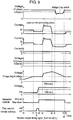
- Fig. 9 is a timing diagram showing the operation of the power supply unit according to the fourth embodiment of the present invention.
- Fig. 9 includes time-lapse change of voltage V1 of power source 22, time-lapse change of current I1 from power source 22, time-lapse change of current I5 to a DC/DC converter, time-lapse change of current I2 to load 21, time-lapse change of voltage V2 at load 21, time-lapse change of voltage V3 of auxiliary power supply 30, time-lapse change of voltage V4 of a capacitor for sample and hold, a switching timing diagram of selector switch 66, and an on-off timing diagram of first and second sample switches 82, 86.
- a component same as that in Figs. 1 , 6 is given the same reference mark to omit its detailed description.
- An arrow in Fig. 8 means the same as that in Fig. 6 .
- the fourth embodiment includes a case where a voltage drop at power source 22 occurs in the same way as in the first embodiment, selection switch 23 is provided to prevent backflow of output from DC/DC converter 24 to power source 22. Accordingly, the operation of selection switch 23 is corresponding to that switching between output from power source 22 and that from DC/DC converter 24 as a power source to load 21 in the same way as in the first embodiment.
- voltage V2 applied to load 21 retains a constant value as well, as shown in Fig. 9 . These are because control is performed so that load 21 always consumes constant current I2 and because constant voltage V2 is always retained within an operable voltage range while the vehicle is being used, in the same way as in the third embodiment.
- Auxiliary power supply 30 is charged until target voltage is reached as shown in Fig. 9 , and thus voltage V3 of auxiliary power supply 30 temporally rises from a low state at time t0.
- auxiliary power supply 30 is fully charged
- control is performed so as not to charge auxiliary power supply 30.
- auxiliary power supply 30 is charged to a charge-target voltage between an uncharged state and fully charged state.
- auxiliary power supply 30 is made to have a margin for an absorbed portion so that it can absorb and charge whenever a large current generating period begins.
- the auxiliary power supply 30 is preliminarily charged to a level at which auxiliary power supply 30 can supply load 21 with power whenever a voltage drop period begins. Therefore, control is performed so that charge-target voltage is always retained in a normal state by discharging power absorbed promptly after a large current generating period ends and by charging a portion of power used promptly after a voltage drop period ends.
- the capacity of auxiliary power supply 30 is to be a sum of a capacity required for absorbing power during a large current generating period and a capacity is required for discharging during the voltage drop period. With this capacity, a charge-target voltage is set so that an amount of charge is large enough to supply load 21 with power during the voltage drop period.
- capacitor 88 for sample and hold that sets voltage (output voltage) at first I/O terminal 34 of DC/DC converter 24 is not sufficiently charged, and thus voltage V4 of capacitor 88 for sample and hold is in a low state at time t0, as shown in Fig. 9 .
- control circuit 76 turns selector switch 66 to the step-down position as shown in Fig. 9 .
- sample timing signal 27 from the ECU is off, and thus first and second sample switches 82, 86 remain off as shown in Fig. 9 .
- control circuit 76 delivers switching start-up signal 77 to drive switching signal generation circuit 68.
- DC/DC converter 24 charges auxiliary power supply 30 with power from power source 22 because selector switch 66 is turned to the step-down position.
- DC/DC converter 24 performs step-down control so that voltage V3 corresponds to voltage (charge-target voltage) of set voltage source 64. Consequently, voltage V3 increases as time elapses as shown in Fig. 9 .
- control circuit 76 If control circuit 76 is assumed to receive sample timing signal 27 at time t2, control circuit 76 immediately turns on first and second sample switches 82, 86 as shown in Fig. 9 . As a result, in the same way as in the third embodiment, voltage corresponding to voltage V2 currently supplied to load 21 is copied to capacitor 88 for sample and hold. At time t3 when sample and hold complete, voltage V4 becomes stabilized as shown in Fig. 9 , and thus control circuit 76 turns off first and second sample switches 82, 86 to hold voltage V4 remaining constant as shown in Fig. 9 . Simultaneously with that, control circuit 76 changes selector switch 66 to the step-up position as shown in Fig. 9 . With this operation, preparation is made so that auxiliary power supply 30 absorbs regenerative electric power or compensates a voltage drop whenever current I1 increases due to regeneration operation or voltage V1 decreases due to consumption of a large amount of current after time t3.
- the operation allows continuing to supply load 21 with current 12 of almost the same amount as that before regeneration operation as shown in Fig. 9 .
- voltage V5 at first I/O terminal 34 of DC/DC converter 24 becomes an output set value held at time t2, and thus voltages V1 and V2 are almost the same as those before regeneration operation. Consequently, if power source 22 supplies a high voltage as shown by solid line V1(max) and V2(max) in Fig. 9 , the voltage becomes almost the same as them. If power source 22 supplies a low voltage as shown by dotted line V1(min) and V2(min), the voltage becomes almost the same as them. Accordingly, voltage V5 at first I/O terminal 34 can be made follow long-term voltage fluctuation of power source 22 in the same way as in the embodiments first through third. This reduces the possibility that the fluctuation in the difference between voltage from power source 22 and that from auxiliary power supply 30 depending on conditions of power source 22 influences the operation of load 21 as seen conventionally.
- Starter operation is performed when the driver changes step from the brake pedal to the gas pedal during a stop, for example. Accordingly, the ECU transmits sample timing signal 27 to control circuit 76 simultaneously with detecting a step change of the pedals. At the time, the starter has not been operated yet.
- the ECU is assumed to drive the starter at time t6 while electric energy absorbed by auxiliary power supply 30 in regeneration operation is being discharged to load 21.
- This causes a large amount of current to flow from power source 22 to the starter, thereby rapidly decreasing voltage V1 as shown in Fig. 9 .
- power has been already supplied from auxiliary power supply to load 21, and thus power is continuously supplied to load 21 after time t6.
- auxiliary power supply 30 needs to pass a current including that equivalent to current I1. Accordingly, as shown by the time-lapse change of current 15 in Fig. 9 , 15 slightly increases to the negative side at time t6. Consequently, current 12 is stabilized after time t6 and voltage V2 at load 21 is stable as well, as shown in Fig. 9 .
- voltage V2 can be set to nearly the same voltage as that before the starter operation even during the voltage drop period, and thus the output voltage of DC/DC converter 24 can be made follow long-term voltage fluctuation of power source 22.
- this reduces the possibility that the fluctuation in the difference between voltage from power source 22 and that from auxiliary power supply 30 depending on conditions of power source 22 influences the operation of load 21 as seen conventionally.
- Voltage V3 of auxiliary power supply 30 needs to be preliminarily adjusted to a charge-target voltage as described above, and thus control circuit 76 changes selector switch 66 to the step-down position at time t8. With this operation, DC/DC converter 24 performs control so that voltage V3 of auxiliary power supply 30 becomes the charge-target voltage of set voltage source 64. Consequently, voltage V3 reaches the charge-target voltage at time t9 and then maintains the voltage.
- time t8 when selector switch 66 is changed may be any time between t7 and t9. Updating voltage V4 held is performed in the same way as in the first embodiment.
- the above-described structure and operation implement power supply unit 20 in which the difference is always small between the voltage of power source 22 in normal times and the output voltage of DC/DC converter 24 when temporarily fluctuating due to generation of a large amount of current from power source 22 or a voltage drop at power source 22.
- the description is made for the case where a large current generating period due to regeneration operation and a voltage drop period due to starter operation nearly continuously occur, as seen in stop idling function.
- the present invention is applicable to a case where both periods occur at a long time interval as well. In such a case, control has only to be performed so that voltage V3 of auxiliary power supply 30 always becomes a charge-target voltage when whichever period completes, a large current generating period or voltage drop period.
- any storage element may be used as long as it is rapidly charging and discharging (e.g. electric double layer capacitor, electrochemical capacitor) as auxiliary power supply 30.
- electrochemical capacitor its discharge potential cannot be made to 0 V, and thus the charge-target voltage of set voltage source 64 needs to be determined in consideration of the lowest possible voltage at which the electrochemical capacitor operates.
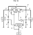
- Fig. 10 is a block circuit diagram of a power supply unit according to the fifth embodiment.
- Fig. 11 is a timing diagram showing the operation of the power supply unit according to the fifth embodiment of the present invention.
- Fig. 11 includes time-lapse change of voltage Va when voltage V1 of a power source is resistively divided with a resistance for detecting voltage V1, time-lapse change of voltage Vb when voltage V2 supplied to a load is resistively divided with resistors 78, 80 for detecting voltage V2, an on-off timing diagram of DC/DC converter start-up signal 29, an on-off timing diagram of a selection switch, an on-off timing diagram of sample timing signal 27, and time-lapse change of voltage V2 supplied to a load.
- Fig. 10 is a block circuit diagram of a power supply unit according to the fifth embodiment.
- Fig. 11 is a timing diagram showing the operation of the power supply unit according to the fifth embodiment of the present invention.
- Fig. 11 includes time-lapse change of voltage Va when voltage V1 of a power source is
- Fig. 12 is a block circuit diagram of a power supply unit with another structure, according to the fifth embodiment.
- Fig. 13 is a timing diagram showing the operation of the power supply unit with another structure, according to the fifth embodiment.
- Fig. 13 includes time-lapse change of voltage Va when voltage V1 of a power source is resistively divided with a resistance for detecting voltage V1, time-lapse change of voltage Vb when voltage V2 supplied to a load is resistively divided with resistors 78, 80 for detecting voltage V2, an on-off timing diagram of DC/DC converter start-up signal 29, an on-off timing diagram of selection switch 23, an on-off timing diagram of sample timing signal 27, and time-lapse change of voltage V2 supplied to a load.
- a component same as that in Fig. 4 is given the same reference mark to omit its detailed description.
- Heavy lines indicate wiring of the power system; thin lines, the control system.
- a description is made in the same way as in the second embodiment, in a vehicle with stop idling function, for example, for the structure in which, when voltage of a power source (composed of a battery and a generator) drops, the voltage of the power source is stepped up and its DC output is supplied to a load.
- Fig. 10 Power is supplied to load 21 through either of the following two paths as shown by the heavy lines in Fig. 10 .
- One is a path through which power from power source 22 is directly supplied through selection switch 23, and the other, supplied through DC/DC converter 24.
- the fifth embodiment is structured so that selection switch 23 is on-off controllable according to an external signal, and is composed of an FET, for example.
- This voltage Vb together with hold voltage Vh output from output terminal OUT of sample-and-hold circuit 28 is input to operational amplifier 94. Output from operational amplifier 94 is input to feedback terminal F/B of DC/DC converter 24.
- Sample timing signal 27 delivered from the engine ECU is input to hold terminal "hold" of sample-and-hold circuit 28 and also to on-off terminal ON/OFF as a start-up signal for DC/DC converter 24. Further, sample timing signal 27 is inverted by inverting circuit 74 to perform on-off control of selection switch 23.
- sample-and-hold circuit 28 is different from those in the embodiments first through fourth.
- hold terminal "hold” When hold terminal "hold” is off, voltage at input terminal IN is directly output from output terminal OUT. After that, when hold terminal "hold” is on, voltage at input terminal IN is held, and voltage Vh held always continues to be output from output terminal OUT. To update hold voltage Vh, hold terminal "hold” is turned off, and then turned on when desired.
- voltage V1 of power source 22 is directly supplied to load 21 because selection switch 23 is on. Consequently, as shown in Fig. 11 , voltage Vb becomes voltage corresponding to voltage Va, and voltage V2 is equal to voltage V1.
- sample timing signal 27 is a signal that turns on before the engine stops and remains on until the engine completes restart. Consequently, sample timing signal 27 is at least on state from the engine stops until the engine completes restart.
- time t1 shows a case where sample timing signal 27 has been delivered nearly at the same time as the engine stops as shown in Fig. 11 .
- sample timing signal 27 is on at time t1.
- This turns on hold terminal "hold" of sample-and-hold circuit 28, and thus voltage Va corresponding to voltage V1 of power source 22 is held and the voltage value (hold voltage Vh) is output from output terminal OUT.
- DC/DC converter start-up signal 29 (equivalent to sample timing signal 27 in the fifth embodiment) turns on and is input to on-off terminal ON/OFF to start up DC/DC converter 24.
- the on-off signal of selection switch 23 is an inverted start-up signal for DC/DC converter 24, the on-off signal becomes off. Resultingly, selection switch 23 is off.
- sample timing signal 27 when sample timing signal 27 turns on at a time before voltage V1 of power source 22 drops (here, time t1 when voltage V1 start to drops), voltage Va corresponding to voltage V1 of power source 22 is held by sample-and-hold circuit 28, DC/DC converter 24 is started up, and selection switch 23 is turned off.
- sample timing signal 27 may be turned on at any time before voltage V1drops.
- sample timing signal 27 is turned on too early, voltage V1 cannot be held even if voltage V1 fluctuates before sample timing signal 27 is turned on, deteriorating the control accuracy of voltage V2 output from DC/DC converter 24, and thus sample timing signal 27 is desirably turned on immediately before voltage V1 drops to the extent as possible.
- DC/DC converter 24 controls output voltage V2 according to a feedback signal from operational amplifier 94 so that voltage Vb corresponding to voltage V2 output from DC/DC converter 24 becomes voltage Vh held by sample-and-hold circuit 28. Consequently, as shown by the time-lapse change of Va in Fig. 11 , even if a voltage drop at power source 22 occurs due to a stop of the generator, voltage Vb corresponding to output voltage V2 becomes equal to hold voltage Vh as shown in the time-lapse change of Vb in Fig. 11 , which does not cause a voltage drop. Consequently, as shown by time-lapse change of V2 in Fig. 11 , voltage V2 remains equal to voltage V1 after time t1, thereby continuously supplying load 21 with power at stable voltage.
- sample timing signal 27 remains on at time t4, and thus, as shown in Fig. 11 , DC/DC converter start-up signal 29 is on and continues its operation.
- Selection switch 23 remains off as shown in Fig. 11 . Consequently, even if voltage Va has recovered at time t4, output from DC/DC converter 24 continues to be supplied to load 21.
- DC/DC converter 24 operates to continue supplying load 21 with voltage corresponding to hold voltage Vh during the voltage drop period (time t1 to t4) of voltage Va shown in Fig. 11 , and thus V2 is stable as shown in Fig. 11 even if voltage V1 of power source 22 largely fluctuates. Consequently, load 21 can continue to be driven.
- sample timing signal 27 is off at time t5 after time t4 when the engine completes restart. However, sample timing signal 27 may become off at time t4. In this case, the operating time of DC/DC converter 24 is decreased, thereby reducing power consumption.
- DC/DC converter 24 continues its operation even after voltage V1 of power source 22 has recovered to the level before stop idling, where voltage (target control voltage) that DC/DC converter 24 is going to output is nearly equal to voltage V1. Consequently, as voltage V2 output from DC/DC converter 24 becomes equal to voltage V1, intermittent operation performed, which causes a voltage ripple in output from DC/DC converter 24 during the period from t4 to t5.
- power supply unit 20 may have a circuit configuration shown in Fig. 12 .
- k is a positive numeric value less than 1.
- k 0.9 so that voltage V2 is 10% lower than voltage V1 when held.
- Fig. 13 Time-lapse change of voltage V2 output from DC/DC converter 24 with such a structure is shown in Fig. 13 .
- Fig. 13 is completely the same as Fig. 11 except voltage V2, and thus its description is omitted.
- DC/DC converter 24 continues its operation from time t6 to t7 even if voltage V1 has been recovered.
- the target control voltage is k times lower than voltage V1 after recovery, and thus DC/DC converter 24 does not perform unstable intermittent operation, unlike in the structure of Fig. 10 . Accordingly, stable voltage V2 with a voltage ripple hardly occurring can continue to be output.
- the above-described structure and operation implement power supply unit 20 in which the difference is always small between the voltage of power source 22 in normal times and the output voltage of DC/DC converter 24 when temporarily fluctuating due to a voltage drop at power source 22.
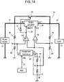
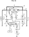
- Fig. 14 is a block circuit diagram of a power supply unit according to the sixth embodiment.
- Fig. 15 is a timing diagram showing the operation of the power supply unit according to the sixth embodiment Fig. 15 includes time-lapse change of voltage Va when voltage V1 of power source is resistively divided with a resistance for detecting voltage V1, time-lapse change of voltage Vb when voltage V2 supplied to a load is resistively divided with resistors 78, 80 for detecting voltage V2, an on-off timing diagram of DC/DC converter start-up signal 29, an on-off timing diagram of a selection switch, an on-off timing diagram of sample timing signal 27, and time-lapse change of voltage V2 supplied to a load.
- Fig. 16 is a block circuit diagram of a power supply unit with another structure, according to the sixth embodiment.
- Fig. 17 is a timing diagram showing the operation of the power supply unit with another structure, according to the sixth embodiment.
- Fig. 17 includes time-lapse change of voltage Va when voltage V1 of a power source is resistively divided with a resistance for detecting voltage V1, time-lapse change of voltage Vb when voltage V2 supplied to a load is resistively divided with a resistance for detecting voltage V2, an on-off timing diagram of DC/DC converter start-up signal 29, an on-off timing diagram of a selection switch, an on-off timing diagram of sample timing signal 27, and time-lapse change of voltage V2 supplied to a load.
- Fig. 18 is a block circuit diagram of a power supply unit with yet another structure, according to the sixth embodiment of the present invention. Fig.
- Fig. 19 is a timing diagram showing the operation of the power supply unit with yet another structure, according to the sixth embodiment of the present invention.
- Fig. 19 includes time-lapse change of voltage Va when voltage V1 of a power source is resistively divided with a resistors for detecting voltage V1, time-lapse change of voltage Vb when voltage V2 supplied to a load is resistively divided with resistors 78, 80 for detecting voltage V2, an on-off timing diagram of DC/DC converter start-up signal 29, an on-off timing diagram of a selection switch, an on-off timing diagram of sample timing signal 27, and time-lapse change of voltage V2 supplied to the load.
- a component same as that in Fig. 10 is given the same reference mark to omit its detailed description.
- Heavy lines indicate wiring of the power system, and thin lines, the control system.
- Figs. 15 , 17 , 19 description for the operation shown by heavy dotted lines in Fig. 5 and others are omitted in the same way as in Fig. 11 .
- a description is made in the same way as in the second embodiment, in a vehicle with stop idling function, for example, for the structure in which, when voltage of a power source (composed of a battery and a power generator) drops, the voltage is stepped up and its DC output is supplied to a load.
- threshold voltage Vc is set so as to be lower than hold voltage Vh is to avoid a voltage ripple generated by DC/DC converter 24 intermittently operating.
- sample-and-hold circuit 28 holds voltage Va corresponding to voltage V1 of power source 22.
- threshold voltage Vc that is a hold voltage Vh multiplied by k with resistors 96, 98 for multiplying voltage Vh by a constant is input to operational amplifier 94 and hysteresis comparator 100.
- output from operational amplifier 94 is input to feedback terminal F/B of DC/DC converter 24 as a feedback signal for making voltage Vb to be threshold voltage Vc.
- Hysteresis comparator 100 compares voltage Va with threshold voltage Vc to output a Lo level ("off signal” hereinafter) if Va > Vc, and a Hi level ("on signal” hereinafter) if Va ⁇ Vc.
- a Lo level if Va > Vc
- a Hi level if Va ⁇ Vc.
- output from hysteresis comparator 100 is an off signal, and thus DC/DC converter start-up signal 29 remains off as shown in Fig. 15 .
- DC/DC converter 24 remains stopping at time t1.
- an off signal of hysteresis comparator 100 is inverted by inverting circuit 74, and thus selection switch 23 remains on at time t1 as shown in Fig. 15 .
- sample timing signal 27 may be turned on at any time before voltage V1drops, where desirably immediately before voltage V1 drops as possible.
- sample timing signal 27 turns off at time t7 after the engine completes restart as shown in Fig. 15 .
- voltage V2 and Vb corresponding to it remain unchanged as shown in Fig. 15 .
- DC/DC converter 24 operates to continue supplying load 21 with voltage corresponding to threshold voltage Vc, from time t1 to t2 and from time t5 to t6, a voltage value corresponding to a voltage between hold voltage Vh and threshold voltage Vc is supplied. Consequently, as shown in Fig. 15 , stable voltage V2 continues to be output even if voltage V1 of power source 22 largely fluctuates, thereby continuing to drive load 21.
- sample timing signal 27 turns off at time t7, namely after time t6 when the engine completes restart. However, it may turn off at time t6.
- Fig. 17 The operation of such power supply unit 20 is shown in Fig. 17 .
- the only different operation is the behavior of voltage Vb during the voltage drop period (time t1 to t6). That is, hold voltage Vh is input to the non-inverting input of operational amplifier 94, and thus in Fig. 17 , control is performed so that voltage Vb becomes hold voltage Vh in the voltage drop period. Accordingly, the time-lapse change characteristic of Vb in Fig. 17 is the same as that of Vb in Fig. 13 . Consequently, final output voltage V2 in the voltage drop period is equal to that in Fig. 13 , which is also equal to that in Fig. 15 as well.
- Fig. 14 The structure of Fig. 14 is applicable to the case where voltage V1 of power source 22 returns to a level nearly close to the voltage before stop idling when the engine completes restart after stop idling. However, if voltage V1 returns to a level lower than the voltage before stop idling when the engine completes restart, output from hysteresis comparator 100 does not turn off, resulting in DC/DC converter 24 continuing to operate.
- Fig. 18 a circuit configuration for avoiding such a state is shown in Fig. 18 .
- the structure of Fig. 18 is different from that of Fig. 14 in that AND circuit 101 is provided into which output from hysteresis comparator 100 and sample timing signal 27 are respectively input, and that output from AND circuit 101 is connected to on-off terminal ON/OFF of DC/DC converter 24 and inverting circuit 74.
- AND circuit 101 is provided into which output from hysteresis comparator 100 and sample timing signal 27 are respectively input, and that output from AND circuit 101 is connected to on-off terminal ON/OFF of DC/DC converter 24 and inverting circuit 74.
- Such power supply unit 20 is shown in Fig. 19 .
- the operation from time t0 to t5 is the same as that of Fig. 15 , and thus its description is omitted.
- DC/DC converter 24 does not continue its operation even if voltage V1 returns to a voltage lower than the voltage before stop idling when the engine completes restart, thereby reducing power consumption of DC/DC converter 24.
- the resistances of resistors 78, 80 for detecting voltage V2 may be set to k times those of resistors 90, 92 for detecting voltage V1, and hold voltage Vh may be input to the non-inverting input of operational amplifier 94.
- the above-described structure and operation implement power supply unit 20 in which the difference is always small between the voltage of power source 22 in normal times and the output voltage of DC/DC converter 24 when temporarily fluctuating due to voltage drop of power source 22.
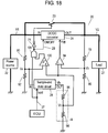
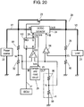
- Fig. 20 is a block circuit diagram of a power supply unit according to the seventh embodiment.
- Fig. 21 is a timing diagram showing the operation of the power supply unit according to the seventh embodiment.
- Fig. 21 includes time-lapse change of voltage Va when voltage V1 of the power source is resistively divided with a resistance for detecting voltage V1, time-lapse change of voltage Vb when voltage V2 supplied to a load is resistively divided with resistors 78, 80 for detecting voltage V2, an on-off timing diagram of DC/DC converter start-up signal 29, an on-off timing diagram of a selection switch, an on-off timing diagram of sample timing signal 27, and time-lapse change of voltage V2 supplied to the load.
- a component same as that in Fig. 14 is given the same reference mark to omit its detailed description.
- Heavy lines indicate wiring of the power system, and thin lines, the control system.
- Fig. 21 description for the operation shown by heavy dotted lines in Fig. 5 and others is omitted in the same way as in Fig. 11 .
- a description is made, in a vehicle with stop idling function, for example, for the structure in which, when voltage of a power source (composed of a battery and a power generator) drops, the voltage is stepped up and its DC output is supplied to a load.
- Fig. 20 Compared with the structure of Fig. 14 , the structural features of Fig. 20 are (1) through (4) below.
- sample timing signal 27 delivered from the ECU is a pulse signal delivered only when stop idling is started. Therefore, completion of an engine restart cannot be detected from sample timing signal 27.
- V1 is approximately 14 V (i.e. maximum value) and voltage Va corresponding to voltage V1 is at its maximum value.
- a stop idling state is assumed to be entered at time t1.
- Hold voltage Vh at this moment is multiplied by k (0.9) with resistors 96, 98 for multiplying voltage Vh by a constant, and threshold voltage Vc obtained is input to operational amplifier 94.
- Vh > Vc is as described in the sixth embodiment. Accordingly, voltage V2 output from DC/DC converter 24 is a predetermined constant times (k times) lower than voltage V1 of power source 22 when held.
- threshold voltage Vc is also input to hysteresis comparator 100, where Va > Vc at time t1 as is clear from Fig. 21 . Accordingly, output from hysteresis comparator 100 becomes an on signal to input 1 to reset terminal R of reset-set flip-flop circuit 102. At this moment, however, 1 is being input to set terminal S, and thus output from DC/DC converter 24 is supplied to load 21. Control is performed so that voltage V2 output from DC/DC converter 24 becomes voltage corresponding to threshold voltage Vc, where Va > Vc from time t1 to t2 as shown by the time-lapse change of Va in Fig. 21 .
- DC/DC converter 24 operates so as to almost directly output voltage at input terminal IN from output terminal OUT. Consequently, as shown in Fig. 21 , voltage V2 decreases according to voltage V1 decreasing, and so does voltage Vb corresponding to voltage V2 as shown in Fig. 21 .
- pulse sample timing signal 27 is assumed to turn off at time t3.
- 0 is input to set terminal S of reset-set flip-flop circuit 102.
- 0 continues to be input to reset terminal R because Va ⁇ Vc as described above.
- Va ⁇ Vc as described above.
- sample timing signal 27 when sample timing signal 27 turns on at a time point before voltage V1 of power-source 22 drops (here, time t1 when voltage Vlstart to drop), voltage Va corresponding to voltage V1 of power source 22 is held by sample-and-hold circuit 28 while DC/DC converter 24 is to be started up and selection switch 23 is to be turned off.
- sample timing signal 27 may be turned on at any time before voltage Vldrops, the time being desirably immediately before voltage V1 drops as possible.
- DC/DC converter 24 operates so as to continue supplying load 21 with voltage corresponding to threshold voltage Vc, and from time t6 to t7, voltage value corresponding to that between hold voltage Vh and threshold voltage Vc is supplied. Consequently, load 21 is stably driven even if voltage of power source 22 largely fluctuates.
- DC/DC converter 24 can be operated only when needed in the same way as in the sixth embodiment.
- the resistances of resistors 78, 80 for detecting voltage V2 may be set to k times those of resistors 90, 92 for detecting voltage V1, and hold voltage Vh may be input to the non-inverting input of operational amplifier 94.
- final output voltage V2 is the same as the time-lapse change characteristic of V2 in Fig. 21 , where the time-lapse change characteristic of Vb in Fig. 21 is merely replaced by the time-lapse change in Fig. 17 , and thus whichever structure may be employed.
- the above-described structure and operation implement power supply unit 20 in which the difference is always small between the voltage of power source 22 in normal times and the output voltage of DC/DC converter 24 when temporarily fluctuating due to a voltage drop at power source 22.
- predetermined constant k is set to 0.9, but an arbitrary number can be set.
- predetermined constant k is set low (e.g. as shown by ta and tb in the time-lapse change of Va in Fig. 21 )
- DC/DC converter 24 can be made to perform step-up operation only during the period from time ta to tb during which voltage Va corresponding to voltage V1 is too low to drive load 21 although DC/DC converter 24 has been started up.
- a power supply unit supplies a load with voltage corresponding to the voltage of a power source in normal times of the power source even when voltage of the power source temporarily fluctuates, thereby continuing to stably operate the load. Therefore, the power supply unit is useful because it compensates a voltage drop at the power source such as a battery producing voltage fluctuation over a long duration according to an environment change.
Landscapes
- Engineering & Computer Science (AREA)
- Power Engineering (AREA)
- Business, Economics & Management (AREA)
- Emergency Management (AREA)
- Dc-Dc Converters (AREA)
- Charge And Discharge Circuits For Batteries Or The Like (AREA)
Description
- The present invention relates to a power supply unit compensating voltage fluctuation of a power source.
- In recent years, to protect the earth environment from the aspect of improving fuel efficiency especially in automobiles, technologies have been developed such as stop idling, electromotive power steering, electromotive turbocharger, and brake regeneration. Among these technologies, stop idling, electromotive power steering, and electromotive turbocharger, for example, consume a large amount of current on the order of 100 amperes to activate a starter, steering motor, and turbine drive motor, respectively, thus causing a voltage drop in a power source composed of such as a battery and power generator. A large voltage drop prevents a load powered from the power source from operating satisfactorily. Performing brake regeneration generates a regenerative current on the order of a maximum of 100 amperes, depending on the vehicle speed, thereby increasing the voltage of the power source. Directly supplying such voltage causes supply voltage to the load to increase, possibly preventing normal operation.
- As a method of eliminating such influence of temporary voltage fluctuation of a power source, the following measure is proposed against a voltage drop, for example, in
Patent Document 1. That is, a voltage drop protection circuit is provided between the battery and auxiliaries. The voltage drop protection circuit may use either of the following method. That is, one includes a capacitor as an auxiliary power supply as described inPatent Document 1, and the voltage is compensated by supplying auxiliaries with power from the capacitor when the battery voltage drops. The other does not include an auxiliary power supply, but the voltage is compensated by raising the voltage of the battery to supply to auxiliaries when the battery voltage drops. - In either of the methods, the voltage drop protection circuit requires a DC/DC converter that converts voltage of a capacitor and/or battery to that required for operation of auxiliaries. Here, a description is made for a concrete example of a voltage drop protection circuit including a capacitor as an auxiliary power supply, using
Fig. 22 . - In
Fig. 22 , voltagedrop protection circuit 1 includes a DC/DC converter circuit configuration, where its input is connected to the output throughcoil 2 anddiode 3. The connecting point of the cathode ofdiode 3 with the output is connected to the ground throughcapacitor 4. Further, the connecting points ofcoil 2 withdiode 3 are connected to the ground throughtransistor 5, and the base oftransistor 5 is connected to the output fromcontroller 6.Controller 6 monitors output voltage of voltagedrop protection circuit 1 to on-offcontrol transistor 5. Operation ofcontroller 6 is controlled according to an on-off signal from the outside. - In such voltage
drop protection circuit 1,transistor 5 is on-off controlled bycontroller 6 operating according to an operation on-off signal and chargescapacitor 4 with voltage increased by means ofcoil 2. Additionally,controller 6 monitors output voltage of voltagedrop protection circuit 1 to maintain the voltage at a predetermined output set value. Consequently, even in a low-voltage state of the battery, the output voltage of voltagedrop protection circuit 1 can be controlled so as not to decrease. The above is an example of a power supply unit compensating a voltage drop of a power source. - The example in
Patent Document 1 compensates a voltage drop of a battery. Meanwhile, output voltage of voltagedrop protection circuit 1 may be suppressed by storing power in brake regeneration tocapacitor 4, for example. - It is true that such a conventional power supply unit can supply a load with stable voltage even if voltage of a power source fluctuates. However, the problem lies in the fact that the voltage output set value of
controller 6 is constant. That is, a battery or the like as a power source produces voltage fluctuation relatively small (concretely, a range between approximately 12 V and 14 V) over a long duration according to an environment change such as fluctuation in ambient temperature and/or deterioration. For this reason, the output set value ofcontroller 6 is fixed to a value (e.g. 11 V) lower than the lowest value (12 V) in a long-term voltage fluctuation range of the battery in order to output power from the battery preferentially in normal times, during which a temporary voltage fluctuation of the battery does not occur. With this arrangement, when the normal battery voltage is approximately 12 V (i.e. lowest value), power is supplied to the load with the output voltage fromcapacitor 4 controlled to be 11 V if the battery voltage temporarily decreases due to such as driving the starter. Accordingly, the load can be kept driven without problems because the supply voltage decreases from 12 V to 11 V at lowest from the viewpoint of the load. If the regular battery voltage is 14 V, however, the voltage results in suddenly decreasing from 14 V to 11 V (the gap is as high as 3 V) from the viewpoint of the load because voltagedrop protection circuit 1 outputs a constant voltage of 11 V due to a temporary drop of the battery voltage. This can possibly affect operation depending on a load. - When performing regeneration by braking, the voltage of the power source temporarily increases as well, and thus
controller 6 operates so as to chargecapacitor 4 when a certain predetermined voltage (e.g. 14.5 V) is exceeded. At this moment, if the voltage of such as a battery before regeneration is 14 V, the voltage fluctuation is small, however if the battery voltage is 12 V, the supply voltage to the load suddenly increases to 14.5 V, which can possibly affect the load in the same way as the above. - Patent Document 1: Japanese Patent Unexamined Publication No.
2005-112250 EP 1209549 A2 discloses a power supply with the features of the preamble ofclaim 1. Japanese Patent ApplicationJP H04 251522 A - To address the above problems, the present invention provides a power supply unit in which the difference is always small between the voltage of a power source in normal times and the output voltage of a DC/DC converter when the voltage of the power source fluctuates.
- A power supply unit of the present invention includes a sample-and-hold circuit that samples voltage corresponding to the voltage supplied from a power source to a load according to
sample timing signal 27 and holds the voltage as an output set value of the DC/DC converter. When the voltage of the power source fluctuates, the power supply unit controls the output voltage of the DC/DC converter so as to be the output set value. By supplying the load with power with the output voltage controlled as explained above, the power supply unit can follow long-term voltage fluctuation of the power source. This structure enables voltage before the voltage of the power source temporarily fluctuates to be an output set value. - With a power supply unit of the present invention, the output set value of a DC/DC converter is updated to a value corresponding to the voltage of the power source immediately before voltage fluctuation, and thus even if the voltage of the power source in normal times fluctuates due to environmental influence, the output voltage of the DC/DC converter is controlled according to the fluctuation. This enables the difference is always small between the voltage of a power source in normal times and the output voltage of a DC/DC converter when the voltage of the power source fluctuates, thereby keeping the load stably operated.
-
-
Fig. 1 is a block circuit diagram of a power supply unit according to the first embodiment of the present invention. -
Fig. 2 is a timing diagram showing the operation of the power supply unit according to the first embodiment of the present invention. -
Fig. 3 is a block circuit diagram of a power supply unit with another structure, according to the first embodiment of the present invention. -
Fig. 4 is a block circuit diagram of a power supply unit according to the second embodiment not forming part of the present invention. -
Fig. 5 is a timing diagram showing the operation of the power supply unit according to the second embodiment. -
Fig. 6 is a block circuit diagram of a power supply unit according to the third embodiment of the present invention. -
Fig. 7 is a timing diagram showing the operation of the power supply unit according to the third embodiment of the present invention. -
Fig. 8 is a block circuit diagram of a power supply unit according to the fourth embodiment of the present invention. -
Fig. 9 is a timing diagram showing the operation of the power supply unit according to the fourth embodiment of the present invention. -
Fig. 10 is a block circuit diagram of a power supply unit according to the fifth embodiment not forming part of the present invention. -
Fig. 11 is a timing diagram showing the operation of the power supply unit according to the fifth embodiment. -
Fig. 12 is a block circuit diagram of a power supply unit with another structure, according to the fifth embodiment. -
Fig. 13 is a timing diagram showing the operation of the power supply unit with another structure, according to the fifth embodiment. -
Fig. 14 is a block circuit diagram of a power supply unit according to the sixth embodiment not forming part of the present invention. -
Fig. 15 is a timing diagram showing the operation of the power supply unit according to the sixth embodiment. -
Fig. 16 is a block circuit diagram of a power supply unit with another structure, according to the sixth embodiment. -
Fig. 17 is a timing diagram showing the operation of the power supply unit with another structure, according to the sixth embodiment. -
Fig. 18 is a block circuit diagram of a power supply unit with yet another structure, according to the sixth embodiment. -
Fig. 19 is a timing diagram showing the operation of the power supply unit with yet another structure, according to the sixth embodiment. -
Fig. 20 is a block circuit diagram of a power supply unit according to the seventh embodiment not forming part of the present invention. -
Fig. 21 is a timing diagram showing the operation of the power supply unit according to the seventh embodiment. -
Fig. 22 is a block circuit diagram of the voltage drop protection circuit of a conventional power supply unit. -
- 20
- Power supply unit
- 21
- Load
- 22
- Power source
- 23
- Selection switch
- 24
- DC/DC converter
- 25
- Third switch
- 26
- Sample timing signal
- 27
- Sample-and-hold circuit
- 28
- DC/DC converter start-up signal
- 30
- Auxiliary power supply
- 32
- Rectifier element
- 40
- First switch
- 42
- Second switch
- 66
- Selector switch
- 68
- Switching signal generation circuit
- 76
- Control circuit
- Hereinafter, a description is made for some preferred embodiments with reference to the related drawings.
-
Fig. 1 is a block circuit diagram of a power supply unit according to the first embodiment of the present invention.Fig. 2 is a timing diagram showing the operation of the power supply unit according to the first embodiment of the present invention.Fig. 2 includes time-lapse change of voltage V1 ofpower source 22, time-lapse change of voltage V2 supplied to load 21, time-lapse change of voltage V3 ofauxiliary power supply 30, time-lapse change of voltage V4 ofcapacitor 88 for sample and hold, an on-off timing diagram ofthird switch 26, a switching timing diagram ofselector switch 66, and an on-off timing diagram of first and second sample switches 82, 86.Fig. 3 is a block circuit diagram of a power supply unit with another structure, according to the first embodiment of the present invention. - In the first embodiment, a description is made for the structure in which, when voltage of the power source drops due to such as driving a starter, power of the auxiliary power supply is voltage-converted by a DC/DC converter, and DC output is supplied to the load.
- In
Fig. 1 ,power supply unit 20 supplies load 21 with power, where they are electrically connected to each other.Power supply unit 20 comprisespower source 22 including a battery and generator,selection switch 23, DC/DC converter 24,third switch 26, sample-and-hold circuit 28, andauxiliary power supply 30 including a capacitor capable of charging and discharging. - Here,
selection switch 23 switches between output frompower source 22 and output from DC/DC converter 24 as a powersource supplying load 21 with power. Concretely,selection switch 23 is composed of a diode to automatically change so as to supplyload 21 with power fromauxiliary power supply 30 when voltage V1 ofpower source 22 drops. This prevents a current output fromauxiliary power supply 30 through DC/DC converter 24 from flowing back topower source 22 when voltage V1 temporarily drops. - DC/
DC converter 24 is a bidirectional converter capable of charging and dischargingauxiliary power supply 30 with a single circuit. Further,third switch 26 hasrectifier element 32 in parallel therewith and can be on-off controlled externally, and an FET is used as third switch in the first embodiment. In this case,rectifier element 32 works as a body diode of the FET. Here, a capacitor used forauxiliary power supply 30 is an electric double-layer capacitor that has excellent rapid charge-discharge characteristic and large capacity. With these structure, DC/DC converter 24 obtains output voltage frompower source 22 orauxiliary power supply 30. - One end of
third switch 26 is connected to first Input/Output (I/O)terminal 34 of DC/DC converter 24, and the other end is connected to the connecting point ofselection switch 23 andload 21. Consequently,power source 22 is connected to DC/DC converter 24 throughthird switch 26. Here,rectifier element 32 is connected so that first I/O terminal 34 side is an anode. - Next, a description is made for the detailed structure of DC/
DC converter 24. First, first I/O terminal 34 has smoothingcapacitor 38 connected thereto betweenterminal 34 andground 36 for smoothing output in step-up operation. Here, the capacitance of the electric double-layer capacitor ofauxiliary power supply 30 is larger than a capacitance of smoothingcapacitor 38. - Both ends of smoothing
capacitor 38 have two switches (first switch 40, second switch 42) series-connected thereto. Here,first switch 40 andsecond switch 42 can be externally controlled so as to alternately repeat on-off operation. FETs are used as first andsecond switches third switch 26. Therefore,body diodes Fig. 1 .First switch 40 is connected to a positive electrode side of smoothingcapacitor 38 so that voltage between the positive and negative electrodes of second I/O terminal 48 of DC/DC converter 24 becomes higher as on-time offirst switch 40 becomes longer. - The connecting point of
first switch 40 withsecond switch 42 is connected to one end of coil 50 (i.e. inductance element). The other end ofcoil 50 is connected to the positive electrode of second I/O terminal 48 giving and receiving power to and fromauxiliary power supply 30. Here, a smoothing capacitor for smoothing output is not provided in the first embodiment, however it may be provided between the positive and negative electrodes of second I/O terminal 48. - To detect voltage V5 at first I/
O terminal 34, tworesistors O terminal 34 andground 36. With these resistors, voltage at the connecting point ofresistors first error amplifier 56 and connecting an output set value determined by sample-and-hold circuit 28 to the other input terminal,first error amplifier 56 outputs an error between them to make voltage V5 equivalent to the output set value whenauxiliary power supply 30 discharges (i.e. in step-up operation of DC/DC converter 24 in the first embodiment). The detailed structure of sample-and-hold circuit 28 is described later. - In the same way, to detect voltage V3 at the positive electrode of second I/
O terminal 48, tworesistors O terminal 48 and the negative electrode ofauxiliary power supply 30. With these resistors, the voltage at the connecting point ofresistors second error amplifier 62 and connecting setvoltage source 64 to the other input terminal,second error amplifier 62 outputs an error between them to make voltage V3 corresponding to the output set value when charging auxiliary power supply 30 (i.e. in step-down operation of DC/DC converter 24 in the first embodiment). - The output terminal of
first error amplifier 56 and that ofsecond error amplifier 62 are connected toselector switch 66 for selecting either one of them. Thisselector switch 66 switches between step-up and step-down operation. That is, whenselector switch 66 selects the output offirst error amplifier 56, step-up operation fromauxiliary power supply 30 to load 21 is to be performed; whenselector switch 66 selects the output fromsecond error amplifier 62, step-down operation frompower source 22 toauxiliary power supply 30 is to be performed. - Output selected by
selector switch 66 is input to switchingsignal generation circuit 68. Switchingsignal generation circuit 68 compares a signal having been input with output fromoscillation circuit 70 usingcomparator 72, generates a pulse signal for turning on and offfirst switch 40 andsecond switch 42, divides an input into two, and inputs one of them to invertingcircuit 74 to generate on and off signals mutually inverted. These signals are separately input tofirst switch 40 andsecond switch 42 to perform voltage conversion (i.e. step-up and step-down of DC/DC converter 24). Here, switching control ofselector switch 66, operation control of switchingsignal generation circuit 68, on-off control ofthird switch 26, and operation control of sample-and-hold circuit 28 are performed bycontrol circuit 76. Of these, the operation of switchingsignal generation circuit 68 is controlled by receiving switching start-upsignal 77 fromcontrol circuit 76. - Next, a description is made for the detailed structure of sample-and-
hold circuit 28. Sample-and-hold circuit 28 has a function to sample voltage corresponding to voltage V2 currently supplied frompower source 22 to load 21 according tosample timing signal 27 delivered from an external unit, e.g. from an engine ECU, and to hold it as an output set value of DC/DC converter 24. - First, to sample voltage V2, two
resistors load 21 andground 36. With these resistors, voltage at the connecting point ofresistors resistors load 21 andground 36, a current frompower source 22 results in always flowing intoresistors first sample switch 82 is series-connected so thatresistors - The connecting point of
resistors capacitor 88 for sample and hold throughvoltage follower 84 andsecond sample switch 86. With this connection, after voltage proportional to voltage V2 at the connecting point is copied tocapacitor 88 for sample and hold,second sample switch 86 is turned off to hold voltage corresponding to voltage V2. Therefore, first and second sample switches 82, 86 are controlled bycontrol circuit 76 so as to be simultaneously turned on only during sample and hold operation. The voltage output copied tocapacitor 88 for sample and hold is input tofirst error amplifier 56 as an output set value of DC/DC converter 24. If voltage V4 ofcapacitor 88 for sample and hold previously held is higher than voltage corresponding to voltage V2 required to be held this time,voltage follower 84 is used as a circuit configuration capable of decreasing voltage V4 to voltage corresponding to voltage V2. Thisvoltage follower 84 allows electric charge ofcapacitor 88 for sample and hold to automatically escape through the ground terminal (not shown) ofvoltage follower 84 until voltage V4 decreases to voltage corresponding to voltage V2. - Here, a description is made for setting of the resistances of
resistors - In this first embodiment, the output set value of DC/
DC converter 24 is determined so that, when voltage V1 ofpower source 22 drops, voltage supplied fromauxiliary power supply 30 to load 21 is lower than the voltage supplied frompower source 22 to load 21 in normal times. This reason is described later in the description for operation. - To determine an output set value in this way, voltage lower than that supplied from
source 22 to load 21 has only to be preliminarily held as an output set value, by way of example. Concretely,resistors - However, DC/
DC converter 24 performs control so that voltage V5 of first I/O terminal 34 becomes an output set value.Rectifier element 32 is connected between first I/O terminal 34 andload 21, thereby causing a voltage drop. Consequently, simply using a resistance with which the voltage decreases at a constant rate results in an excessively low output voltage fromauxiliary power supply 30 by the voltage drop. Accordingly, the output set value of DC/DC converter 24 is preliminarily raised by voltage corresponding to a voltage drop atrectifier element 32. - From all of the above, the resistances of
resistors rectifier element 32. - Here, an output set value of DC/
DC converter 24 is determined by setting resistances ofresistors resistors - Next, a description is made for the operation of
power supply unit 20 having a structure described above, usingFigs. 1 ,2 . - The assumption is made that voltage V1 of
power source 22 is a certain constant value whenpower supply unit 20 starts up (time t0) as shown inFig. 2 . InFig. 2 , voltage V1 is shown by a solid line V1(max) and a dotted line V1(min), showing a fluctuation range ofpower source 22 according to a change in ambient temperature or a deterioration, where the maximum value of voltage V1 is indicated by a solid line and the minimum by a dotted line. - At time t0, since a temporary voltage drop is not occurring in
power source 22, power frompower source 22 is supplied to load 21 throughselection switch 23. Consequently, as shown inFig. 2 , voltage V2 applied to load 21 is constant within the range between solid line V2 (max) and dotted line V2(min) corresponding to the fluctuation range of voltage V1. - At this moment, since
power supply unit 20 is in a state immediately after start-up,auxiliary power supply 30 has not been charged yet. Consequently, as shown inFig. 2 , voltage V3 ofauxiliary power supply 30 is in a low state at time t0. - In the same way, immediately after
power supply unit 20 starts up, sincecapacitor 88 for sample and hold that sets output voltage of DC/DC converter 24 has not been charged, voltage V4 ofcapacitor 88 for sample and hold is in a low state at time t0 as shown inFig. 2 . - In this state immediately after start-up,
auxiliary power supply 30 needs to be fully charged, to compensate a temporary voltage drop ofpower source 22, like in a case when operating a starter after stop idling. For this reason,control circuit 76 turns onthird switch 26 and setsselector switch 66 to the step-down position as shown inFig. 2 . Meanwhile, sincesample timing signal 27 from the ECU is off immediately after start-up, first and second sample switches 82, 86 remain off as shown inFig. 2 . - In this state,
control circuit 76 delivers switching start-upsignal 77 to drive switchingsignal generation circuit 68. Sinceselector switch 66 has been switched to the step-down position, DC/DC converter 24 chargesauxiliary power supply 30 with power frompower source 22. In this case, DC/DC converter 24 performs control for step-down operation so that voltage V3 corresponds to the voltage of setvoltage source 64. Consequently, as shown inFig. 2 , voltage V3 increases as time elapses. - Then, when voltage V3 becomes corresponding to the voltage of set
voltage source 64, DC/DC converter 24 operates so that voltage V3 maintains voltage corresponding to that of setvoltage source 64. Consequently, voltage V3 is stabilized as shown inFig. 2 . - After that, the assumption is made that the starter is operated to restart the engine after the stop idling of the automobile. Starter operation is performed when a driver changes step from a brake pedal to a gas pedal during a stop, for example. At this moment, the ECU transmits sample timing signal 27 (pulse signal) to control
circuit 76 simultaneously with detecting a step change of the pedals. At the time, the starter has not been operated yet. - When
control circuit 76 receivessample timing signal 27 at time t1,control circuit 76 immediately turns offthird switch 26 and at the same time turns on first and second sample switches 82, 86 as shown inFig. 2 . Consequently, by turning offthird switch 26,control circuit 76 cuts power input frompower source 22, at first. Meanwhile, by turning on first and second sample switches 82, 86,control circuit 76 copies voltage V2 currently supplied to load 21 tocapacitor 88 for sample and hold as a voltage proportional to voltage V2 resistively divided withresistors capacitor 88 for sample and hold reaches a voltage corresponding to voltage V2. Under the circumstances, as shown inFig. 2 , first and second sample switches 82, 86 are kept on until time t2 (preliminarily determined) when voltage V4 is stabilized with sufficient charge accumulated. - At time t2, voltage V4 becomes stabilized and voltage corresponding to voltage V2 has been sampled. Then, control
circuit 76 turns off first and second sample switches 82, 86 as shown inFig. 2 to hold voltage V4 remaining constant and simultaneously changesselector switch 66 to the step-up position. With this operation, whenever the starter is driven to drop voltage V1,auxiliary power supply 30 is ready to supplyload 21 with power. - After that, the ECU is assumed to drive the starter at time t3. This causes a large amount of current to flow from
power source 22 to the starter, thereby rapidly dropping voltage V1 as shown inFig. 2 . At this moment, since DC/DC converter 24 has been switched to step-up operation, voltage ofauxiliary power supply 30 is increased and supplied to load 21 immediately. - Here, the output voltage of DC/
DC converter 24 is controlled so as to be an output set value held at time t2. Consequently, after time t3, voltage V2 can be voltage nearly the same as that before the starter is operated. Consequently, ifpower source 22 provides a high voltage value as shown by the solid line of voltage V2 inFig. 2 , a voltage close to the voltage value is supplied to load 21. Meanwhile, ifpower source 22 provides a low voltage value as shown by the dotted line of voltage V2, a voltage close to the voltage value is supplied to load 21. Accordingly, by performing variance control on the output voltage of DC/DC converter 24 so that voltage V4 sampled by sample-and-hold circuit 28 becomes the output set value, the output voltage can follow long-term voltage fluctuation ofpower source 22. This reduces the possibility that the fluctuation in the difference between the voltage frompower source 22 and that the voltage fromauxiliary power supply 30 influences the operation ofload 21 depending on conditions ofpower source 22, as seen conventionally. - In the first embodiment, as shown in
Fig. 2 , arrangement is made so that voltage fromauxiliary power supply 30 is slightly lower than the voltage frompower source 22. This is because the embodiment is structured so that voltage lower than that supplied frompower source 22 to load 21 is preliminarily held as an output set value. The reason for such a structure is to avoid the following possibility. That is, if voltage fromauxiliary power supply 30 is higher than the voltage frompower source 22, power is supplied fromauxiliary power supply 30 to load 21 even if voltage V1 is not low, and the starter has not been operated yet from time t2 to time t3. This causes insufficient power supplied fromauxiliary power supply 30 when actually required. Setting the resistances ofresistors hold circuit 28. - During the voltage drop period of voltage V1, power is supplied from
auxiliary power supply 30 to load 21, and thus voltage V3 decreases as time lapses after time t3 as shown inFig. 2 . - Then, the assumption is made that starting the engine completes at time t4 and the operation of the starter stops. At this moment, voltage V1 rapidly recovers the voltage before its drop as shown in
Fig. 2 . As, the output voltage of DC/DC converter 24 is set to a level slightly lower than the voltage ofpower source 22, supplyingload 21 with output from DC/DC converter 24 is stopped byrectifier element 32, and power supply frompower source 22 continues. Resultingly, voltage V2 slightly rises and then stays stabilized as shown inFig. 2 . Meanwhile, as supplyingload 21 with output from DC/DC converter 24 stops, voltage V3 remains constant at a voltage at time t4. - After that, to fully charge
auxiliary power supply 30 again,control circuit 76 turns onthird switch 26 at time t5 and changesselector switch 66 to the step-down position as shown inFig. 2 . Since this state is the same as that at time t0, the operation same as that from time t0 to time t1 chargesauxiliary power supply 30. Consequently, voltage V3 increases after time t5 as shown inFig. 2 , and when fully charged, operation is performed so as to maintain the voltage. - By repeating the above-described operation, voltage V2 van be maintained at nearly the same voltage even if voltage V1 decreases.
- Here, as shown in
Fig. 2 , after time t5, voltage V4 continues maintaining the voltage held. Ifsample timing signal 27 is received again in this state to turn on first and second sample switches 82, 86, voltage V4 is updated to voltage corresponding to voltage V2 at the time, where if voltage V4 is lower than voltage corresponding to voltage V2,capacitor 88 for sample and hold is charged until voltage corresponding to voltage V2 is reached. Meanwhile, if voltage V4 is higher than voltage corresponding to voltage V2, discharge is made fromcapacitor 88 for sample and hold to the ground ofvoltage follower 84 to a level at which voltage corresponding to voltage V2 is reached as described in the structure of sample-and-hold circuit 28. In this way, sample-and-hold circuit 28 with the structure of the first embodiment enables voltage V4 to be automatically updated to a voltage corresponding to voltage V2 only by turning on first and second sample switches 82, 86. - The above-described structure and operation provide
power supply unit 20 in which the difference is always small between voltage ofpower source 22 in normal times and output voltage of DC/DC converter 24 when the voltage ofpower source 22 drops. - In the first embodiment, the example is shown where DC/
DC converter 24 step ups the voltage ofauxiliary power supply 30 to supplyload 21 with power. However, the following structure provides the same advantages. That is, a well-known step-down type converter, or step-up and step-down type converters may be used as DC/DC converter 24 that steps down the high voltage ofauxiliary power supply 30 to supply power fromauxiliary power supply 30 to load 21. - In the first embodiment, the structure is shown in which
power source 22 andauxiliary power supply 30 are connected in parallel through DC/DC converter 24. However,power source 22 may be series-connected toauxiliary power supply 30 as shown inFig. 3 . In this case, the other circuit configuration is the same as that ofFig. 1 except that the step-up and step-down positions ofselector switch 66 are inverted. In the circuit configuration ofFig. 3 , the voltage to chargeauxiliary power supply 30 needs to be higher than voltage V1 ofpower source 22 , and thus DC/DC converter 24 is to perform step-up operation when charging. Consequently, during a voltage drop period ofpower source 22, high voltage V3 ofauxiliary power supply 30 is stepped down and supplied to load 2. Accordingly, step-up and step-down operation of DC/DC converter 24 is to be inverted from the operation ofFig. 1 , and thus the step-up and step-down positions of the selector switch inFig. 2 need to be inverted. Temporal operation other than this is the same as that ofFig. 2 . However, the voltage drop characteristic of voltage V3 during the voltage drop period (time t3 to t4) of voltage V3 inFig. 2 is not linear, but has a characteristic given by being combined with fluctuation of voltage V1 during the period t3 to t4 inFig. 2 . In other words, it is a characteristic (not shown) in which the voltage is decreasing like the time-lapse change of voltage V3 inFig. 2 as a whole while including short-term voltage fluctuation of V1. - With such a structure, in addition to the advantage obtained from the structure of
Fig. 1 , voltage is stepped down and supplied to load 21 during a voltage drop period, contrarily to the case ofFig. 1 , thus resulting in the advantage in that a current flowing is reduced proportionately with a high voltage, and a loss in DC/DC converter 24 is reduced. - In the first embodiment, even after
auxiliary power supply 30 is fully charged, for example, DC/DC converter 24 continues to be operated to maintain the fully charged voltage. However, the electric double-layer capacitor with a large capacitance used inauxiliary power supply 30 prevents the voltage from rapidly decreasing even if DC/DC converter 24 is stopped. Therefore, DC/DC converter 24 may be operated only whileauxiliary power supply 30 is being charged or discharged. In this case, while DC/DC converter 24 is at a stop, it does not consume power. Accordingly, in addition to the primary advantage that enables stable operation of a load with reduced voltage fluctuation, further efficientpower supply unit 20 is obtained. - In the first embodiment, the example is shown where a bidirectional converter is used as DC/
DC converter 24, but the invention can use a conventional DC/DC converter with diode rectification as well. -
Fig. 4 is a block circuit diagram of a power supply unit according to the second embodiment.Fig. 5 is a timing diagram showing the operation of the power supply unit according to the second embodiment.Fig. 5 includes time-lapse change of voltage V1, time-lapse change of supply voltage V2 to load 21, time-lapse change of voltage V4 ofcapacitor 88 for sample and hold, an on-off timing diagram of switching start-upsignal 77, and an on-off timing diagram of first and second sample switches 82, 86. InFigs. 4 ,5 , a component same as that inFigs. 1 ,2 is given the same reference mark to omit its detailed description. In the second embodiment, a description is made for the structure in which, when voltage of a power source (composed of a battery and a power generator) drops, the voltage is stepped up and its DC output is supplied to a load. - First, the structural differences between
Fig. 4 andFig. 1 are (1) through (4) as described below. - (1)
Auxiliary power supply 30 is eliminated, andpower source 22 is connected to second I/O terminal 48 to whichauxiliary power supply 30 has been connected. - (2) Following this change, a step-up converter is used as DC/
DC converter 24. - (3) Consequently, step-down control becomes unnecessary, thus resistors 58, 60 for detecting voltage V3,
second error amplifier 62, setvoltage source 64, andselector switch 66 are eliminated. - (4) Since charge operation for
auxiliary power supply 30 by DC/DC converter 24 becomes unnecessary,third switch 26 andrectifier element 32 are eliminated, which results in voltage V5 of first I/O terminal 34 being equal to voltage V2 to load 21. - Although the structures other than the above differences are the same as those in the first embodiment, since
rectifier element 32 is not present, its voltage drop does not need to be considered in setting the resistances ofresistors - Next, a description is made for the operation of
power supply unit 20 with such a structure, usingFigs. 4 ,5 . - The assumption is made that voltage V1 of
power source 22 is a certain constant value whenpower supply unit 20 starts up (time t0) as shown inFig. 5 . Here, solid lines V1(max), V2(max) and dotted lines V1(min), V2(min) inFig. 5 mean the same as those inFig. 2 . - Since a temporary voltage drop of
power source 22 does not occur at time t0, power frompower source 22 is supplied to load 21 throughselection switch 23. Consequently, as shown inFig. 5 , voltage V2 atload 21 remains constant within the range between the solid line and broken line corresponding to the fluctuation range of voltage V1. - At this moment,
power supply unit 20 is in a state immediately after start-up, and thuscapacitor 88 for sample and hold that sets output voltage of DC/DC converter 24 is not charged. Consequently, voltage V4 ofcapacitor 88 for sample and hold is in a low state at time t0 as shown inFig. 5 . - In this state immediately after start-up, a temporary voltage drop of
power source 22 does not occur, and thus DC/DC converter 24 does not need to be started up. Therefore,control circuit 76 keeps switching start-upsignal 77 off as shown inFig. 5 . In the same way,sample timing signal 27 from the ECU is off immediately after start-up, and thus first and second sample switches 82, 86 remain off as well as shown inFig. 5 . - Then, after the automobile stops idling, for example, when the starter is activated to restart the engine, the ECU delivers sample timing signal 27 (pulse signal) to control
circuit 76 immediately before activating the starter. - If
control circuit 76 is assumed to receivesample timing signal 27 at time t1,control circuit 76 immediately turns on first and second sample switches 82, 86 as shown inFig. 5 . Consequently, voltage V2 currently supplied to load 21 is copied tocapacitor 88 for sample and hold as voltage proportional to voltage V2 resistively divided withresistors capacitor 88 for sample and hold reaches voltage corresponding to voltage V2. Under the circumstances, as shown inFig. 5 , first and second sample switches 82, 86 are kept on until time t2 (preliminarily determined) when voltage V4 is stabilized with sufficient charge accumulated. - At time t2, voltage V4 becomes stable and voltage corresponding to voltage V2 results in having been sampled. Under the circumstances,
control circuit 76 turns off first and second sample switches 82, 86 as shown inFig. 5 to hold voltage V4 remaining constant and simultaneously turns on switching start-upsignal 77 as shown inFig. 5 . - Here, as described later, voltage V2 output from DC/
DC converter 24 is set to a level slightly lower than output voltage V1 ofpower source 22. However, since DC/DC converter 24 of the second embodiment is of step-up type, it cannot convert the voltage V2 lower than input voltage V1 of DC/DC converter 24 at time t2. In this case, switchingsignal generation circuit 68 performs control so as to operate for the lowest possible step-up ratio, namely to operate so thatsecond switch 42 remain off andfirst switch 40 remain on. Consequently, DC/DC converter 24 results in being activated so as to step up the voltage ofpower source 22 to be able to supplyload 21 whenever the starter is driven to drop voltage V1. This results in power supply frompower source 22 to load 21 executed by means of wiring throughselection switch 23 and of wiring through the series circuit ofcoil 50 andfirst switch 40. - After that, the ECU is assumed to drive the starter at time t3. Then, a large amount of current flows from
power source 22 to the starter, which causes voltage V1 to be droped rapidly as shown inFig. 5 . At this moment, although voltage V2 simultaneously drops, step-up operation can be started at a time point when voltage V2 decreases to an output set value, because DC/DC converter 24 has been already started up. Consequently, DC/DC converter 24 steps up the low voltage ofpower source 22 and immediately supplies power from first I/O terminal 34 to load 21, thereby stabilizing voltage V2. - Here, output voltage of DC/
DC converter 24 is controlled so as to be an output set value held at time t2. Consequently, as described in the first embodiment, voltage V2 can be set to nearly the same voltage as the voltage before the starter operation. This reduces the possibility that the fluctuation in the difference of voltage V2 between before and after the starter operation, that depends on conditions ofpower source 22 and influences the operation ofload 21 as seen conventionally. - In the second embodiment, as shown in the characteristic of voltage V2 in
Fig. 5 , the voltage from DC/DC converter 24 is set to a level slightly lower than the voltage frompower source 22 because of the following reason. If the voltage from DC/DC converter 24 is higher than the voltage frompower source 22, power is supplied from DC/DC converter 24 to load 21 even when the starter has not been operated yet and voltage V1 has not been decreased during the period from time t2 to time t3. In this case, DC/DC converter 24 produces a loss, and thus such voltage setting is made to reduce any unnecessary power consumption due to the loss. - Next, the assumption is made that the engine start completes at time t4 to stop the starter operation. At this moment, as shown in
Fig. 5 , voltage V1 rapidly recovers the voltage before its drop. Consequently, as described above,second switch 42 of DC/DC converter 24 remains off andfirst switch 40 remains on because the output voltage of DC/DC converter 24 is set to a level slightly lower than that frompower source 22. At this moment, power to load 21 is continuously supplied through the wiring ofselection switch 23 and that of the series circuit ofcoil 50 andfirst switch 40. Resultingly, voltage V2 slightly rises and then stays stabilized as shown inFig. 5 . - After that, to stop the operation of DC/
DC converter 24,control circuit 76 turns off switching start-upsignal 77 at time t5 as shown inFig. 5 , resulting in the same state as that at time t0. - By repeating the above-described operation, voltage V2 can be maintained at a level nearly the same even if voltage V1 drops. Here, updating voltage V4 after time t5 is performed with the same operation as that in the first embodiment.
- The above-described structure and operation provide
power supply unit 20 in which the difference is always small between the voltage ofpower source 22 in normal times and the output voltage of DC/DC converter 24 when the voltage ofpower source 22 drops. - In the second embodiment, control is performed so as to stop the operation of DC/
DC converter 24 when switching start-upsignal 77 is off. However, in normal times during which the voltage ofpower source 22 is not low, namely when switching start-upsignal 77 is off, switchingsignal generation circuit 68 may be operated so that onlyfirst switch 40 connected between the input and output of DC/DC converter 24 (i.e. between first I/O terminal 34 and second I/O terminal 48) is turned on. With this method, power is supplied frompower source 22 to load 21 through DC/DC converter 24 even when switching start-upsignal 77 is off. When operated in this way, voltage V2 becomes equal to voltage V1 becausefirst switch 40 is on in normal times. Consequently, voltage V4 sampled and held becomes correspond to voltage V1, and thus the output voltage of DC/DC converter 24 is not subject to the influence of a voltage drop atselection switch 23, thereby further reducing the difference between voltage supplied to load 21 in normal times and that when the voltage ofpower source 22 drops. Accordingly, the advantage is available in that voltage V2 is further stabilized. In this case, power frompower source 22 is supplied to load 21 throughcoil 50 andfirst switch 40, and the wiring throughselection switch 23 may be eliminated. - In the second embodiment, the description is made for the structure in which
rectifier element 32 is not provided. However,rectifier element 32 may be provided at the same position as that in the first embodiment. Herewith, even if smoothingcapacitor 38,first switch 40, orsecond switch 42 fails with a short circuit in the worst case, a problem in which a current frompower source 22 flows to ground 36 is prevented, thereby improving the reliability. In this case, however, the resistances ofresistors rectifier element 32 in the same way as in the first embodiment. - In the second embodiment, the example is shown where a synchronously rectifying step-up converter is used as DC/
DC converter 24, but a conventional DC/DC converter with diode rectification may be used. - The structures described in the first and second embodiments may be applied to a large current consuming system such as an electromotive power steering and electromotive turbocharger in addition to stop idling.
-
Fig. 6 is a block circuit diagram of a power supply unit according to the third embodiment of the present invention.Fig. 7 is a timing diagram showing the operation of the power supply unit according to the third embodiment of the present invention.Fig. 7 includes time-lapse change of current I1 frompower source 22, time-lapse change of current I5 to DC/DC converter, time-lapse change of current 12 to load 21, time-lapse change of voltage V2 atload 21, time-lapse change of voltage V3 ofauxiliary power supply 30, time-lapse change of voltage V4 ofcapacitor 88 for sample and hold, a switching timing diagram ofselector switch 66, and an on-off timing diagram of first and second sample switches 82, 86. InFig. 6 , a component same as that inFig. 1 is given the same reference mark to omit its detailed description. An arrow inFig. 6 indicates a current flow, where the direction of the arrow is defined as a positive current. - In the third embodiment, a description is made for the following case. That is, when the voltage of a power source temporarily rises due to such as regeneration of braking energy to electric energy, this rising fluctuation portion is voltage-converted by a DC/DC converter and absorbed by an auxiliary power supply, and power of the auxiliary power supply is discharged in normal times when regeneration is not performed.
- First, the structural differences between
Fig. 6 andFig. 1 are (1) through (3) below. - (1) In the third embodiment, a description is made for a case where a voltage drop at
power source 22 as in the first embodiment does not occur, and thus output from DC/DC converter 24 does not backflow to powersource 22. Consequently,selection switch 23 for preventing backflow is unnecessary and eliminated. - (2) In the first embodiment,
third switch 26 is provided so that excessive power does not flow out to outside unless necessary whenauxiliary power supply 30 is fully charged. In the third embodiment,third switch 26 is eliminated so that regenerated power is ready to be used for charge any time. Following this,rectifier element 32 is eliminated as well. - (3) The chargeable capacity of
auxiliary power supply 30 is set to a level at which all the maximum electric energy in regeneration can be absorbed. - The other structures other than the above are the same as those in the first embodiment. However, since
rectifier element 32 is not present as well as in the second embodiment, its voltage drop does not need to be considered in setting the resistances ofresistors power source 22 becomes equal to that fromauxiliary power supply 30 is selected. - Next, a description is made for the operation of
power supply unit 20 , usingFigs. 6 ,7 . - In normal times (time t0) after
power supply unit 20 completes start-up, current I1 flowing frompower source 22 is assumed to be a constant value consumed byload 21 as shown inFig. 7 . - Meanwhile, although
auxiliary power supply 30 is in a state discharged at time t0, control needs to be performed so thatauxiliary power supply 30 is not charged in order to collect all the energy generated by regeneration. Accordingly,auxiliary power supply 30 has circuit configuration in which it is charged through DC/DC converter 24, and thus control is performed so that current I5 to DC/DC converter 24 becomes zero as shown inFig. 7 . An electric double layer capacitor fully dischargeable is used asauxiliary power supply 30. - If
load 21 is assumed to be always consuming constant current I2 while the vehicle is being used, constant current I2 flows throughload 21 at time t0 as shown inFig. 7 , and thus I1 = I2 at time t0. - Meanwhile, voltage V2 applied to load 21 is controlled so as to be always constant within an operable voltage range while the vehicle is being used, and thus voltage V2 remains constant at time t0 as shown in
Fig. 7 . Here, solid lines V2(max) and dotted lines V2(min) inFig. 7 mean the same as those inFig. 2 . -
Auxiliary power supply 30 is not charged at time t0 as described above, and thus voltage V3 ofauxiliary power supply 30 is zero as shown inFig. 7 . - When
power supply unit 20 completes start-up,capacitor 88 for sample and hold that sets voltage (output voltage) at first I/O terminal 34 of DC/DC converter 24 is not sufficiently charged, and thus voltage V4 ofcapacitor 88 for sample and hold is in a low state at time t0 as shown inFig. 7 . - Here, a description is made for the operation of each switch using timing diagrams.
- First, to prevent
auxiliary power supply 30 from being charged at time t0,control circuit 76 performs control so thatselector switch 66 selects the step-down position (second error amplifier 62 side). The set voltage of setvoltage source 64 connected tosecond error amplifier 62 is set to the lowest possible voltage (e.g. 1 V) at which DC/DC converter 24 can perform step-up operation, and thus with the above-described selection, DC/DC converter 24 is charge-controlled so that voltage V3 ofauxiliary power supply 30 becomes the set voltage. Onceauxiliary power supply 30 is charged, the charge operation stops. - Next, since
sample timing signal 27 from the ECU is off at time t0, both of the first and second sample switches 82 and 86 remain off as shown inFig. 7 . - The driver is assumed to execute braking operation in this state. With this operation, a braking signal is input to the ECU on the vehicle from the brake pedal. With the signal, the ECU immediately delivers
sample timing signal 27 to controlcircuit 76. At the time point, the power generator has not performed regeneration yet. - If
control circuit 76 is assumed to receivesample timing signal 27 at time t1,control circuit 76 immediately turns on first and second sample switches 82, 86 as shown inFig. 7 . Consequently, in the same way as in the first embodiment, voltage corresponding to voltage V2 currently supplied to load 21 is copied tocapacitor 88 for sample and hold. At this moment, time for charging is required to at least a voltage V4 ofcapacitor 88 for sample and hold reaches voltage corresponding to voltage V2. Under the circumstances, as shown inFig. 7 , first and second sample switches 82, 86 are kept on until time t2 (preliminarily determined) when voltage V4 becomes stabilized with sufficient charge accumulated. - At time t2, voltage V4 becomes stable and voltage corresponding to voltage V2 results in having been sampled. Then, control
circuit 76 turns off first and second sample switches 82, 86 as shown inFig. 7 to hold voltage V4 constant, and simultaneously switchesselector switch 66 to the step-up position as shown inFig. 7 . At this moment, operation is performed so that output of DC/DC converter 24 becomes voltage immediately before (voltage held). Consequently,auxiliary power supply 30 is hardly charged or discharged until a regenerative current is generated. Whenever current I1 increases after time t2 due to regeneration, preparation is made with the operation so that the increase is absorbed by chargingauxiliary power supply 30 with regenerative electric power. - After that, regeneration operation for vehicle braking is assumed to start at time t3. This causes a large amount of current to flow from
power source 22 temporarily, thereby rapidly increasing current I1 as shown inFig. 7 . At this moment, DC/DC converter 24 performs control so that voltage V5 at first I/O terminal 34 becomes voltage V4 sampled and held, and thus temporary fluctuating current I5 due to regeneration as shown inFig. 7 is absorbed by chargingauxiliary power supply 30 to lower an increase of voltage V5 according to an increase of current I1 to voltage V4. - The operation allows continuing to supply
load 21 with current I2 of almost the same amount as before the regeneration as shown inFig. 7 . - Further, control is performed so that voltage V5 at first I/
O terminal 34 of DC/DC converter 24 becomes an output set value held at time t2, and thus voltage V2 is almost the same voltage as that the voltage before regeneration operation. Consequently, ifpower source 22 supplies a high voltage as shown by the solid line inFig. 7 , voltage V2(max) almost the same as the high voltage is supplied to load 21. Ifpower source 22 supplies a low voltage as shown by the dotted line, voltage V2(min) almost the same as the low voltage is supplied to load 21. Accordingly, by exercising variance control on output voltage of DC/DC converter 24 so that voltage V4 sampled by sample-and-hold circuit 28 becomes the output set value, voltage V5 at first I/O terminal 34 can be made follow long-term voltage fluctuation ofpower source 22 in the same way as in the first and second embodiments. This reduces the possibility that the fluctuation in the difference between voltage frompower source 22 and that fromauxiliary power supply 30 depending on conditions ofpower source 22 influences the operation ofload 21 as seen conventionally. - In the third embodiment, power is not supplied from
auxiliary power supply 30 to load 21 during a voltage drop period ofpower source 22 as seen in the first embodiment, and thus the possibility does not exist inherently that power fromauxiliary power supply 30 becomes deficient when necessary. Consequently, an output set value does not need to be set so that voltage fromauxiliary power supply 30 is slightly lower than the voltage frompower source 22 as shown by the time-lapse change of current I5 inFig. 2 . Accordingly, as shown inFig. 7 , even during a large current generating period due to regeneration operation, voltage V2 is to be almost the same voltage as in normal times when the regeneration operation does not take place. This operation reduces fluctuation in voltage to load 21 to the extent as soon as possible. - During a large current generating period, temporary fluctuation portion I5 of current I1 of
power source 22 is absorbed by chargingauxiliary power supply 30 through DC/DC converter 24, and thus voltage V3 temporally increases after time t3 as shown by the time-lapse change of voltage V3 inFig. 7 . - Then, the regeneration operation is assumed to end at time t4. At this moment, as shown in
Fig. 7 , current I1 rapidly decreases and hardly flows frompower source 22. This is because control is performed so that charge power absorbed byauxiliary power supply 30 during a large current generating period is preferentially discharged to prepare for reabsorbing a fluctuation portion of a current in the next large current generating period. - As a result, as shown by the time-lapse change of current I5 in
Fig. 7 , current I5 at first I/O terminal 34 flows in the negative direction to be supplied to load 21 after time t4, resulting in I2 ≒ -I5. Accordingly, as shown by the time-lapse change of current I2 inFig. 7 , the same amount of current I2 is continuously supplied to load 21 after time t4, and as shown by the time-lapse change of voltage V2 inFig. 7 , voltage V2 atload 21 is kept constant. - Following this, as power from
auxiliary power supply 30 is supplied to load 21, voltage V3 temporally decreases after time t4.Auxiliary power supply 30 needs to be completely discharged to absorb a next temporary fluctuation portion of a large amount of current. Under the circumstances,control circuit 76changes selector switch 66 to the step-down position at time t5. With this action, DC/DC converter 24 operates so that voltage V3 ofauxiliary power supply 30 becomes voltage of setvoltage source 64. Consequently, power ofauxiliary power supply 30 is completely discharged and its state is maintained. - Circumstances of the operation at this moment are shown as the time-lapse change of voltage V3 in
Fig. 7 . Voltage V3 becomes 0 V at time t6 and retains 0 V from then on. With such operation, power cannot be supplied fromauxiliary power supply 30 to load 21 after time t6, and thus current I1 is supplied frompower source 22 to load 21 at this time point as shown by the time-lapse change of current I1 inFig. 7 . At this moment,auxiliary power supply 30 has completed discharge as shown by the time-lapse change of current I5 inFig. 7 , and thus current I5 at first I/O terminal 34 becomes zero. - With the above operation, current I2 and voltage V2 to load 21 always retain the same values, enabling
load 21 to continue operating stably. - By repeating the above-described operation, current I2 and voltage V2 can retain the roughly same values even when current I1 increases. Here, time t5 when
selector switch 66 is changed may be any time between t4 and t6. Updating voltage V4 held is executed in the same way as in the first embodiment. - The above-described structure and operation implement
power supply unit 20 in which the difference is always small between the voltage ofpower source 22 in normal times and the output voltage of DC/DC converter 24 when temporarily fluctuating due to a large amount of current frompower source 22. - In the third embodiment, an electric double layer capacitor is used as
auxiliary power supply 30. However, another storage element such as an electrochemical capacitor that is capable of rapidly charging and discharging may be used. -
Fig. 8 is a block circuit diagram of a power supply unit according to the fourth embodiment of the present invention.Fig. 9 is a timing diagram showing the operation of the power supply unit according to the fourth embodiment of the present invention.Fig. 9 includes time-lapse change of voltage V1 ofpower source 22, time-lapse change of current I1 frompower source 22, time-lapse change of current I5 to a DC/DC converter, time-lapse change of current I2 to load 21, time-lapse change of voltage V2 atload 21, time-lapse change of voltage V3 ofauxiliary power supply 30, time-lapse change of voltage V4 of a capacitor for sample and hold, a switching timing diagram ofselector switch 66, and an on-off timing diagram of first and second sample switches 82, 86. InFig. 8 , a component same as that inFigs. 1 ,6 is given the same reference mark to omit its detailed description. An arrow inFig. 8 means the same as that inFig. 6 . - In the fourth embodiment, a description is made for a power supply unit supplying a load with stable power even when both the following occur. That is, a case where both the first and third embodiments are simultaneously performed, namely when voltage of the power source temporarily rises due to such as regeneration operation by braking; and when voltage of the power source temporarily drops due to consumption of a large amount of current by the starter.
- First, the structural differences between
Fig. 8 andFig. 6 are described below. Since the fourth embodiment includes a case where a voltage drop atpower source 22 occurs in the same way as in the first embodiment,selection switch 23 is provided to prevent backflow of output from DC/DC converter 24 topower source 22. Accordingly, the operation ofselection switch 23 is corresponding to that switching between output frompower source 22 and that from DC/DC converter 24 as a power source to load 21 in the same way as in the first embodiment. - The structures other than the above are the same as those in the first and third embodiments. Setting the resistances of
resistors power source 22 becomes the same as that fromauxiliary power supply 30 in the same way as in the third embodiment. - Next, a description is made for the operation of
power supply unit 20 with such a structure, usingFigs. 8 ,9 . - In normal times (time t0) after
power supply unit 20 completes start-up, when neither generation of a large amount of current nor a voltage drop occurs, voltage V1 ofpower source 22 is assumed to be constant as shown inFig. 9 . Here, solid line V1(max) and dotted line V1(min) inFig. 9 mean the same as those in the first embodiment. In this case, current I1 flowing fromcurrent supply source 22 is a constant value corresponding to the sum of consumption current I2 due to drivingload 21 and charging current I5 toauxiliary power supply 30, as shown inFig. 9 . Consequently, charging current I5 toauxiliary power supply 30 and current I2 to load 21 are constant values as well, as shown inFig. 9 . Resultingly, voltage V2 applied to load 21 retains a constant value as well, as shown inFig. 9 . These are because control is performed so thatload 21 always consumes constant current I2 and because constant voltage V2 is always retained within an operable voltage range while the vehicle is being used, in the same way as in the third embodiment. -
Auxiliary power supply 30 is charged until target voltage is reached as shown inFig. 9 , and thus voltage V3 ofauxiliary power supply 30 temporally rises from a low state at time t0. Here, though in the first embodiment,auxiliary power supply 30 is fully charged, in the third embodiment, control is performed so as not to chargeauxiliary power supply 30. In the fourth embodiment, meanwhile,auxiliary power supply 30 is charged to a charge-target voltage between an uncharged state and fully charged state. This is becauseauxiliary power supply 30 is made to have a margin for an absorbed portion so that it can absorb and charge whenever a large current generating period begins., Theauxiliary power supply 30 is preliminarily charged to a level at whichauxiliary power supply 30 can supplyload 21 with power whenever a voltage drop period begins. Therefore, control is performed so that charge-target voltage is always retained in a normal state by discharging power absorbed promptly after a large current generating period ends and by charging a portion of power used promptly after a voltage drop period ends. For this arrangement, the capacity ofauxiliary power supply 30 is to be a sum of a capacity required for absorbing power during a large current generating period and a capacity is required for discharging during the voltage drop period. With this capacity, a charge-target voltage is set so that an amount of charge is large enough to supplyload 21 with power during the voltage drop period. - When
power supply unit 20 completes start-up,capacitor 88 for sample and hold that sets voltage (output voltage) at first I/O terminal 34 of DC/DC converter 24 is not sufficiently charged, and thus voltage V4 ofcapacitor 88 for sample and hold is in a low state at time t0, as shown inFig. 9 . - In this state (time t0) after start-up completes, to compensate a temporary voltage drop of
power source 22 during the voltage drop period,auxiliary power supply 30 needs to be charged to charge-target voltage as described above. For this purpose,control circuit 76 turnsselector switch 66 to the step-down position as shown inFig. 9 . After start-up completes,sample timing signal 27 from the ECU is off, and thus first and second sample switches 82, 86 remain off as shown inFig. 9 . - In this state,
control circuit 76 delivers switching start-upsignal 77 to drive switchingsignal generation circuit 68. With this operation, DC/DC converter 24 chargesauxiliary power supply 30 with power frompower source 22 becauseselector switch 66 is turned to the step-down position. In this case, DC/DC converter 24 performs step-down control so that voltage V3 corresponds to voltage (charge-target voltage) of setvoltage source 64. Consequently, voltage V3 increases as time elapses as shown inFig. 9 . - Then, when voltage V3 becomes voltage corresponding to a voltage of set
voltage source 64, DC/DC converter 24 operates so that voltage V3 maintains voltage corresponding to that the voltage of setvoltage source 64. Consequently, voltage V3 becomes stabilized at time t1 as shown inFig. 9 . This operation completes charge toauxiliary power supply 30, and thus current I5 for chargingauxiliary power supply 30 becomes zero as shown by the time-lapse change of current I5 inFig. 9 . Consequently, current I1 decreases to a level same as load consumption current I2 at time t1 as shown inFig. 9 becausepower source 22 needs to pass only current I2 throughload 21. - In this state, the driver is assumed to perform braking operation. This operation causes a braking signal to be input from the brake pedal to the ECU of the vehicle. With this input, the ECU transmits
sample timing signal 27 to controlcircuit 76 immediately. At this time, the power generator has not performed regeneration operation. - If
control circuit 76 is assumed to receivesample timing signal 27 at time t2,control circuit 76 immediately turns on first and second sample switches 82, 86 as shown inFig. 9 . As a result, in the same way as in the third embodiment, voltage corresponding to voltage V2 currently supplied to load 21 is copied tocapacitor 88 for sample and hold. At time t3 when sample and hold complete, voltage V4 becomes stabilized as shown inFig. 9 , and thus controlcircuit 76 turns off first and second sample switches 82, 86 to hold voltage V4 remaining constant as shown inFig. 9 . Simultaneously with that,control circuit 76changes selector switch 66 to the step-up position as shown inFig. 9 . With this operation, preparation is made so thatauxiliary power supply 30 absorbs regenerative electric power or compensates a voltage drop whenever current I1 increases due to regeneration operation or voltage V1 decreases due to consumption of a large amount of current after time t3. - After that, regeneration operation for vehicle braking is assumed to start at time t4. This causes a large amount of current to flow from
power source 22 temporarily, thereby rapidly increasing current I1 as shown inFig. 9 . At this moment, DC/DC converter 24 performs control so that voltage V5 at first I/O terminal 34 becomes voltage V4 sampled and held, and thus temporary fluctuating current I5 due to regeneration is absorbed by chargingauxiliary power supply 30 through DC/DC converter 24 to lower an increase of voltage V5 according to an increase of current I1 to voltage V4. - The operation allows continuing to supply
load 21 with current 12 of almost the same amount as that before regeneration operation as shown inFig. 9 . - Further, control is performed so that voltage V5 at first I/
O terminal 34 of DC/DC converter 24 becomes an output set value held at time t2, and thus voltages V1 and V2 are almost the same as those before regeneration operation. Consequently, ifpower source 22 supplies a high voltage as shown by solid line V1(max) and V2(max) inFig. 9 , the voltage becomes almost the same as them. Ifpower source 22 supplies a low voltage as shown by dotted line V1(min) and V2(min), the voltage becomes almost the same as them. Accordingly, voltage V5 at first I/O terminal 34 can be made follow long-term voltage fluctuation ofpower source 22 in the same way as in the embodiments first through third. This reduces the possibility that the fluctuation in the difference between voltage frompower source 22 and that fromauxiliary power supply 30 depending on conditions ofpower source 22 influences the operation ofload 21 as seen conventionally. - During a large current generating period,
temporary fluctuation portion 15 of current I1 frompower source 22 is absorbed by chargingauxiliary power supply 30 through DC/DC converter 24, and thus voltage V3 temporally increases after time t4 as shown inFig. 9 . - Then, the assumption is made that the regeneration operation ends and the vehicle stops (stop idling) at time t5. At this moment, current I1 rapidly drops as shown in
Fig. 9 and current I1 hardly flows frompower source 22. This is because control is performed so that charge power absorbed byauxiliary power supply 30 during the large current generating period is preferentially discharged to prepare for reabsorbing a fluctuation portion of a current in the next large current generating period. - As a result, as shown by the time-lapse change of current I5 in
Fig. 9 , current I5 at first I/O terminal 34 flows in the negative direction to be supplied to load 21 after time t5, resulting in I2 ≒ -I5. Accordingly, even when the engine stops for stop idling, as shown by the time-lapse change of current I2 inFig. 9 , the same amount of current I2 is continuously supplied to load 21 after time t5, and as shown inFig. 9 , voltage V2 atload 21 is kept constant. - Following this, as power from
auxiliary power supply 30 is supplied to load 21, voltage V3 temporally decreases after time t5. - After that, the assumption is made that the starter is operated to restart the engine. Starter operation is performed when the driver changes step from the brake pedal to the gas pedal during a stop, for example. Accordingly, the ECU transmits
sample timing signal 27 to controlcircuit 76 simultaneously with detecting a step change of the pedals. At the time, the starter has not been operated yet. - Under normal circumstances, voltage V2 currently supplied to load 21 at this time is copied to
capacitor 88 for sample and hold. However, since the time from regeneration operation until restart of the starter is usually short, during which the environmental temperature and deterioration of the battery are not supposed to change suddenly, voltage V4 already having been sampled and held at time t3 is continuously used here. Therefore, sample and hold operation is not performed after time t5. - After that, the ECU is assumed to drive the starter at time t6 while electric energy absorbed by
auxiliary power supply 30 in regeneration operation is being discharged to load 21. This causes a large amount of current to flow frompower source 22 to the starter, thereby rapidly decreasing voltage V1 as shown inFig. 9 . At this time, power has been already supplied from auxiliary power supply to load 21, and thus power is continuously supplied to load 21 after time t6. - Here, at time t6, nearly all the current from
power source 22 flows to the starter, and thus a small amount of current I1 that was flowing to load 21 at time t5 becomes completely zero at time t6 as shown inFig. 9 . Therefore, to continue passing stable current I2 throughload 21,auxiliary power supply 30 needs to pass a current including that equivalent to current I1. Accordingly, as shown by the time-lapse change of current 15 inFig. 9 ,15 slightly increases to the negative side at time t6. Consequently, current 12 is stabilized after time t6 and voltage V2 atload 21 is stable as well, as shown inFig. 9 . - With such operation, voltage V2 can be set to nearly the same voltage as that before the starter operation even during the voltage drop period, and thus the output voltage of DC/
DC converter 24 can be made follow long-term voltage fluctuation ofpower source 22. In the fourth embodiment as well, this reduces the possibility that the fluctuation in the difference between voltage frompower source 22 and that fromauxiliary power supply 30 depending on conditions ofpower source 22 influences the operation ofload 21 as seen conventionally. - During the voltage drop period of voltage V1, power is supplied from
auxiliary power supply 30 to load 21, and thus as shown in the time-lapse change of voltage V3 inFig. 9 , voltage V3 temporally decreases after time t6. In this case, since current I1 fromcurrent supply source 22 is zero, a declination of voltage V3 from time t6 to t7 is slightly lager than a declination from time t5 to t6. - Then, the assumption is made that the engine completes start-up and the operation of the starter stops at time t7. At this moment, as shown in
Fig. 9 , voltage V1 rapidly recovers to a voltage before the voltage drop. Consequently, the same state as that from time t5 to t6 is entered, and as shown inFig. 9 , a small amount of current I1 flows again frompower source 22. Following this, as shown inFig. 9 , current I5 supplied fromauxiliary power supply 30 to load 21 becomes slightly lower at the negative side. Consequently, as shown inFig. 9 , the declination of voltage V3 ofauxiliary power supply 30 decreases as well. - Voltage V3 of
auxiliary power supply 30 needs to be preliminarily adjusted to a charge-target voltage as described above, and thus controlcircuit 76changes selector switch 66 to the step-down position at time t8. With this operation, DC/DC converter 24 performs control so that voltage V3 ofauxiliary power supply 30 becomes the charge-target voltage of setvoltage source 64. Consequently, voltage V3 reaches the charge-target voltage at time t9 and then maintains the voltage. - When voltage V3 reaches the charge-target voltage, power supply from
auxiliary power supply 30 to load 21 is stopped to maintain the voltage. Consequently, as shown inFig. 9 , load consumption current I2 is supplied frompower source 22 to load 21 at time t9. At this moment, as shown inFig. 9 , power supply fromauxiliary power supply 30 has been stopped, and thus current I5 at first I/O terminal 34 becomes zero. - Even if both a large current generating period and voltage drop period exist, by repeating the above-described operation, current I2 and voltage V2 to load 21 always retain almost the same values as shown in
Fig. 9 , and thus load 21 can continue its operation stably. Here, time t8 whenselector switch 66 is changed may be any time between t7 and t9. Updating voltage V4 held is performed in the same way as in the first embodiment. - The above-described structure and operation implement
power supply unit 20 in which the difference is always small between the voltage ofpower source 22 in normal times and the output voltage of DC/DC converter 24 when temporarily fluctuating due to generation of a large amount of current frompower source 22 or a voltage drop atpower source 22. - In the fourth embodiment, the description is made for the case where a large current generating period due to regeneration operation and a voltage drop period due to starter operation nearly continuously occur, as seen in stop idling function. However, the present invention is applicable to a case where both periods occur at a long time interval as well. In such a case, control has only to be performed so that voltage V3 of
auxiliary power supply 30 always becomes a charge-target voltage when whichever period completes, a large current generating period or voltage drop period. - In the fourth embodiment as well, any storage element may be used as long as it is rapidly charging and discharging (e.g. electric double layer capacitor, electrochemical capacitor) as
auxiliary power supply 30. However, for an electrochemical capacitor, its discharge potential cannot be made to 0 V, and thus the charge-target voltage of setvoltage source 64 needs to be determined in consideration of the lowest possible voltage at which the electrochemical capacitor operates. -
Fig. 10 is a block circuit diagram of a power supply unit according to the fifth embodiment.Fig. 11 is a timing diagram showing the operation of the power supply unit according to the fifth embodiment of the present invention.Fig. 11 includes time-lapse change of voltage Va when voltage V1 of a power source is resistively divided with a resistance for detecting voltage V1, time-lapse change of voltage Vb when voltage V2 supplied to a load is resistively divided withresistors signal 29, an on-off timing diagram of a selection switch, an on-off timing diagram ofsample timing signal 27, and time-lapse change of voltage V2 supplied to a load.Fig. 12 is a block circuit diagram of a power supply unit with another structure, according to the fifth embodiment.Fig. 13 is a timing diagram showing the operation of the power supply unit with another structure, according to the fifth embodiment.Fig. 13 includes time-lapse change of voltage Va when voltage V1 of a power source is resistively divided with a resistance for detecting voltage V1, time-lapse change of voltage Vb when voltage V2 supplied to a load is resistively divided withresistors signal 29, an on-off timing diagram ofselection switch 23, an on-off timing diagram ofsample timing signal 27, and time-lapse change of voltage V2 supplied to a load. - In
Figs. 10 ,12 , a component same as that inFig. 4 is given the same reference mark to omit its detailed description. Heavy lines indicate wiring of the power system; thin lines, the control system. In the fifth embodiment, a description is made in the same way as in the second embodiment, in a vehicle with stop idling function, for example, for the structure in which, when voltage of a power source (composed of a battery and a generator) drops, the voltage of the power source is stepped up and its DC output is supplied to a load. - First, a description is made for the circuit configuration of
Fig. 10 . Power is supplied to load 21 through either of the following two paths as shown by the heavy lines inFig. 10 . One is a path through which power frompower source 22 is directly supplied throughselection switch 23, and the other, supplied through DC/DC converter 24. The fifth embodiment is structured so thatselection switch 23 is on-off controllable according to an external signal, and is composed of an FET, for example. - Voltage V1 of
power source 22 is detected as midpoint voltage Va when voltage V1 is resistively divided withresistors resistors hold circuit 28. - In the same way, voltage V2 at
load 21 is detected as midpoint voltage Vb when voltage V2 is resistively divided withresistors resistors hold circuit 28 is input tooperational amplifier 94. Output fromoperational amplifier 94 is input to feedback terminal F/B of DC/DC converter 24. -
Sample timing signal 27 delivered from the engine ECU is input to hold terminal "hold" of sample-and-hold circuit 28 and also to on-off terminal ON/OFF as a start-up signal for DC/DC converter 24. Further,sample timing signal 27 is inverted by invertingcircuit 74 to perform on-off control ofselection switch 23. - Here, the operation of sample-and-
hold circuit 28 is different from those in the embodiments first through fourth. When hold terminal "hold" is off, voltage at input terminal IN is directly output from output terminal OUT. After that, when hold terminal "hold" is on, voltage at input terminal IN is held, and voltage Vh held always continues to be output from output terminal OUT. To update hold voltage Vh, hold terminal "hold" is turned off, and then turned on when desired. - Next, a description is made for the operation of
power supply unit 20 with such a structure usingFig. 11 . Here, the operation shown by the heavy dotted lines inFig. 5 , for example, is the same as that shown by the heavy solid lines V1(min) and V2(min) inFig. 5 (merely the voltage becomes low), and is omitted inFig. 11 . - First, at time t0, stop idling is not performed and the engine is being driven. At this moment, since the generator is operating as well, voltage V1 of
power source 22 is stable at approximately 14 V, for example. Consequently, voltage Va corresponding to voltage V1 is stable at a high voltage value as shown inFig. 11 . At this time, as shown inFig. 11 , sincesample timing signal 27 from the ECU is off, DC/DC converter start-upsignal 29 to be input to on-off terminal ON/OFF of DC/DC converter 24 remains off and DC/DC converter 24 is in a stopped state.Sample timing signal 27 is inverted by invertingcircuit 74, and thus an on signal is input toselection switch 23 as shown inFig. 11 . Consequently,selection switch 23 turns on. - From these results, voltage V1 of
power source 22 is directly supplied to load 21 becauseselection switch 23 is on. Consequently, as shown inFig. 11 , voltage Vb becomes voltage corresponding to voltage Va, and voltage V2 is equal to voltage V1. - Next, the assumption is made that stop idling is performed to stop the engine at time t1. The ECU delivers
sample timing signal 27 at the time before the engine stops. In the fifth embodiment,sample timing signal 27 is a signal that turns on before the engine stops and remains on until the engine completes restart. Consequently,sample timing signal 27 is at least on state from the engine stops until the engine completes restart. - In the fifth embodiment, time t1 shows a case where
sample timing signal 27 has been delivered nearly at the same time as the engine stops as shown inFig. 11 . Accordingly, as shown inFig. 11 ,sample timing signal 27 is on at time t1. This turns on hold terminal "hold" of sample-and-hold circuit 28, and thus voltage Va corresponding to voltage V1 ofpower source 22 is held and the voltage value (hold voltage Vh) is output from output terminal OUT. Simultaneously with this, as shown inFig. 11 , DC/DC converter start-up signal 29 (equivalent to sample timingsignal 27 in the fifth embodiment) turns on and is input to on-off terminal ON/OFF to start up DC/DC converter 24. Further, as shown inFig. 11 , as the on-off signal ofselection switch 23 is an inverted start-up signal for DC/DC converter 24, the on-off signal becomes off. Resultingly,selection switch 23 is off. - In summary, when
sample timing signal 27 turns on at a time before voltage V1 ofpower source 22 drops (here, time t1 when voltage V1 start to drops), voltage Va corresponding to voltage V1 ofpower source 22 is held by sample-and-hold circuit 28, DC/DC converter 24 is started up, andselection switch 23 is turned off. Here,sample timing signal 27 may be turned on at any time before voltage V1drops. However, ifsample timing signal 27 is turned on too early, voltage V1 cannot be held even if voltage V1 fluctuates beforesample timing signal 27 is turned on, deteriorating the control accuracy of voltage V2 output from DC/DC converter 24, and thus sample timingsignal 27 is desirably turned on immediately before voltage V1 drops to the extent as possible. - As a result of such operation, power is supplied from DC/
DC converter 24 to load 21. DC/DC converter 24 controls output voltage V2 according to a feedback signal fromoperational amplifier 94 so that voltage Vb corresponding to voltage V2 output from DC/DC converter 24 becomes voltage Vh held by sample-and-hold circuit 28. Consequently, as shown by the time-lapse change of Va inFig. 11 , even if a voltage drop atpower source 22 occurs due to a stop of the generator, voltage Vb corresponding to output voltage V2 becomes equal to hold voltage Vh as shown in the time-lapse change of Vb inFig. 11 , which does not cause a voltage drop. Consequently, as shown by time-lapse change of V2 inFig. 11 , voltage V2 remains equal to voltage V1 after time t1, thereby continuously supplyingload 21 with power at stable voltage. - During the period from time t1 (stop idling occurs) to time t2 (after a short period elapses), as shown in
Fig. 11 , voltage Va corresponding to voltage V1 ofpower source 22 drops rapidly, however, it decreases slowly after time t2. Meanwhile, despite such fluctuation of voltage Va, as shown inFig. 11 , voltage Vb corresponding to voltage V2 output from DC/DC converter 24 remains stable at hold voltage Vh, and thus voltage V2 maintains a state equal to voltage V1 when held. - Next, the assumption is made that stop idling ends and the starter is driven to restart the engine at time t3. In this case, since a large amount of current flows through the starter, voltage V1 of
power source 22 rapidly drops to approximately 6 V. Consequently, as shown by the time-lapse change of Va inFig. 11 , voltage Va corresponding to voltage V1 also drops rapidly. After that, as the engine revolution becomes stabilized, an amount of current to the starter decreases to increase voltage Va. When the engine completes restart at time t4, the generator restarts as well, and thus voltage V1 ofpower source 22 returns to a voltage value (approximately 14 V) before the stop idling. Consequently, voltage Va corresponding to voltage V1 recovers the voltage value from time t0 to t1. - However, in the fifth embodiment, as shown in
Fig. 11 ,sample timing signal 27 remains on at time t4, and thus, as shown inFig. 11 , DC/DC converter start-upsignal 29 is on and continues its operation.Selection switch 23 remains off as shown inFig. 11 . Consequently, even if voltage Va has recovered at time t4, output from DC/DC converter 24 continues to be supplied to load 21. - After that, the assumption is made that
sample timing signal 27 from the ECU turns off at time t5 after the time point (time t4) when the engine restarted as shown inFig. 11 . The operation in this case is opposite to that at time t1, namely hold terminal "hold" of sample-and-hold circuit 28 turns off, and thus hold voltage Vh at output terminal OUT of sample-and-hold circuit 28 becomes equal to voltage Va at input terminal IN. As shown inFig. 11 , start-upsignal 29 for DC/DC converter 24 turns off to stop the operation. Further, as shown inFig. 11 ,selection switch 23 turns on, and thus voltage V1 ofpower source 22 is to be applied to load 21 throughselection switch 23. With this operation, the state returns to a state when the engine is in operation, namely the state at time t0. - With such operation, DC/
DC converter 24 operates to continue supplyingload 21 with voltage corresponding to hold voltage Vh during the voltage drop period (time t1 to t4) of voltage Va shown inFig. 11 , and thus V2 is stable as shown inFig. 11 even if voltage V1 ofpower source 22 largely fluctuates. Consequently, load 21 can continue to be driven. - In the fifth embodiment,
sample timing signal 27 is off at time t5 after time t4 when the engine completes restart. However,sample timing signal 27 may become off at time t4. In this case, the operating time of DC/DC converter 24 is decreased, thereby reducing power consumption. - To summarize the operation when the engine restarts described above, as shown in
Fig. 11 , whensample timing signal 27 turns off after the time point (time t4) when voltage Va corresponding to voltage V1 ofpower source 22 recovers to hold voltage Vh, DC/DC converter 24 is to be stopped andselection switch 23 is to be turned on. - In the circuit configuration of
Fig. 10 , as shown inFig. 11 (from time t4 to t5), DC/DC converter 24 continues its operation even after voltage V1 ofpower source 22 has recovered to the level before stop idling, where voltage (target control voltage) that DC/DC converter 24 is going to output is nearly equal to voltage V1. Consequently, as voltage V2 output from DC/DC converter 24 becomes equal to voltage V1, intermittent operation performed, which causes a voltage ripple in output from DC/DC converter 24 during the period from t4 to t5. - If this voltage ripple is problematic,
power supply unit 20 may have a circuit configuration shown inFig. 12 . The structure ofFig. 12 is different from that ofFig. 10 in that the resistances ofresistors DC converter 24 is a predetermined constant times (k times) lower than voltage V1 ofpower source 22 when held. More specifically, assuming the resistances ofresistors resistors - Time-lapse change of voltage V2 output from DC/
DC converter 24 with such a structure is shown inFig. 13 . Here,Fig. 13 is completely the same asFig. 11 except voltage V2, and thus its description is omitted. - As shown at time t1 in
Fig. 13 , whensample timing signal 27 is delivered from the ECU, DC/DC converter 24 turns on andselection switch 23 turns off. With this operation, voltage V2 output from DC/DC converter 24 is applied to load 21. In this case, control is performed so that the target control voltage of DC/DC converter 24 becomes a voltage that is k times voltage V1 ofpower source 22 held at time t1. Consequently, voltage V1 is higher than the target control voltage (= k × V1 = 0.9 × V1) at time t1. Accordingly, DC/DC converter 24, a step-up converter as described above, does not undergo step-up operation even if started up, and thus voltage V1 at input terminal IN is almost directly output from output terminal OUT. - After that, as shown in
Fig. 13 , since voltage Va corresponding to voltage V1 decreases after stop idling is started, where, when voltage V1 becomes the target control voltage at time t2, the voltage value (∝ k × Vh) is output, and after t2, the voltage proportional to k × Vh is maintained. - After that, as a result that stop idling ends and voltage V1 of
power source 22 recovers, when voltage V1 exceeds the target control voltage at time t5, DC/DC converter 24 almost directly outputs voltage V1 at input terminal IN from output terminal OUT as described above. Consequently, voltage V2 increases in the same way as voltage V1 during the period from time t5 to time t6 when voltage V1 completes its recovery, and then voltage V1 becomes stabilized after time t6, so does voltage V2. - After that, as shown in
Fig. 13 , whensample timing signal 27 turns off at time t7, DC/DC converter 24 turns off, and simultaneouslyselection switch 23 turns on. With this operation, voltage V1 is directly applied to load 21, and thus voltage V2 becomes equal to voltage V1. - In such operation, DC/
DC converter 24 continues its operation from time t6 to t7 even if voltage V1 has been recovered. However, the target control voltage is k times lower than voltage V1 after recovery, and thus DC/DC converter 24 does not perform unstable intermittent operation, unlike in the structure ofFig. 10 . Accordingly, stable voltage V2 with a voltage ripple hardly occurring can continue to be output. - The above-described structure and operation implement
power supply unit 20 in which the difference is always small between the voltage ofpower source 22 in normal times and the output voltage of DC/DC converter 24 when temporarily fluctuating due to a voltage drop atpower source 22. -
Fig. 14 is a block circuit diagram of a power supply unit according to the sixth embodiment.Fig. 15 is a timing diagram showing the operation of the power supply unit according to the sixth embodimentFig. 15 includes time-lapse change of voltage Va when voltage V1 of power source is resistively divided with a resistance for detecting voltage V1, time-lapse change of voltage Vb when voltage V2 supplied to a load is resistively divided withresistors signal 29, an on-off timing diagram of a selection switch, an on-off timing diagram ofsample timing signal 27, and time-lapse change of voltage V2 supplied to a load.Fig. 16 is a block circuit diagram of a power supply unit with another structure, according to the sixth embodiment.Fig. 17 is a timing diagram showing the operation of the power supply unit with another structure, according to the sixth embodiment.Fig. 17 includes time-lapse change of voltage Va when voltage V1 of a power source is resistively divided with a resistance for detecting voltage V1, time-lapse change of voltage Vb when voltage V2 supplied to a load is resistively divided with a resistance for detecting voltage V2, an on-off timing diagram of DC/DC converter start-upsignal 29, an on-off timing diagram of a selection switch, an on-off timing diagram ofsample timing signal 27, and time-lapse change of voltage V2 supplied to a load.Fig. 18 is a block circuit diagram of a power supply unit with yet another structure, according to the sixth embodiment of the present invention.Fig. 19 is a timing diagram showing the operation of the power supply unit with yet another structure, according to the sixth embodiment of the present invention.Fig. 19 includes time-lapse change of voltage Va when voltage V1 of a power source is resistively divided with a resistors for detecting voltage V1, time-lapse change of voltage Vb when voltage V2 supplied to a load is resistively divided withresistors signal 29, an on-off timing diagram of a selection switch, an on-off timing diagram ofsample timing signal 27, and time-lapse change of voltage V2 supplied to the load. - In
Figs. 14 ,16 ,18 , a component same as that inFig. 10 is given the same reference mark to omit its detailed description. Heavy lines indicate wiring of the power system, and thin lines, the control system. InFigs. 15 ,17 ,19 , description for the operation shown by heavy dotted lines inFig. 5 and others are omitted in the same way as inFig. 11 . In the sixth embodiment, a description is made in the same way as in the second embodiment, in a vehicle with stop idling function, for example, for the structure in which, when voltage of a power source (composed of a battery and a power generator) drops, the voltage is stepped up and its DC output is supplied to a load. - First, the circuit configuration of
Fig. 14 is described. Compared with the structure ofFig. 10 , the structural features ofFig. 14 are (1) through (3) below. - (1)
Resistors hold circuit 28, and its midpoint voltage Vc (referred to as "threshold voltage Vc" hereinafter) is connected tooperational amplifier 94 and the non-inverting input ofhysteresis comparator 100. Here, resistances R5, R6 are set so that threshold voltage Vc is positive and lower than hold voltage Vh, namely k < 1. In the sixth embodiment, like in the first embodiment, k is determined as k = 0.9 so that threshold voltage Vc is 10% lower than hold voltage Vh, and thus Vc = Vh × R6/(R5 + R6) = 0.9 × Vh. - (2) Voltage Va is input to the inverting input of
hysteresis comparator 100. - (3) Output of
hysteresis comparator 100 is used as a start-up signal for DC/DC converter 24 and connected to on-off terminal ON/OFF and invertingcircuit 74. - (4) Following (3),
sample timing signal 27 is only connected to terminal "hold" of sample-and-hold circuit 28. - Here, the reason why threshold voltage Vc is set so as to be lower than hold voltage Vh is to avoid a voltage ripple generated by DC/
DC converter 24 intermittently operating. As described in the fifth embodiment, the voltage ripple occurs when input voltage V1 of DC/DC converter 24 becomes equal to output voltage V2. That is, with Vh > Vc, DC/DC converter 24 does not enter the state of V1 = V2, causing no voltage ripple, thereby supplyingload 21 with more stable voltage. - Next, a description is made for the operation of such
power supply unit 20 referring toFig. 15 . First, the operation from time t0 to t1 is the same as that in the fifth embodiment, and thus its description is omitted. - The assumption is made that stop idling is performed to turn on
sample timing signal 27 from the ECU at time t1. Consequently, sample-and-hold circuit 28 holds voltage Va corresponding to voltage V1 ofpower source 22. With this operation, threshold voltage Vc that is a hold voltage Vh multiplied by k withresistors operational amplifier 94 andhysteresis comparator 100. As a result, output fromoperational amplifier 94 is input to feedback terminal F/B of DC/DC converter 24 as a feedback signal for making voltage Vb to be threshold voltage Vc.Hysteresis comparator 100 compares voltage Va with threshold voltage Vc to output a Lo level ("off signal" hereinafter) if Va > Vc, and a Hi level ("on signal" hereinafter) if Va < Vc. At time t1, which is immediately after voltage Va is held and k = 0.9, thus Va > Vc as shown inFig. 15 . Consequently, output fromhysteresis comparator 100 is an off signal, and thus DC/DC converter start-upsignal 29 remains off as shown inFig. 15 . Accordingly, DC/DC converter 24 remains stopping at time t1. In the same way, an off signal ofhysteresis comparator 100 is inverted by invertingcircuit 74, and thusselection switch 23 remains on at time t1 as shown inFig. 15 . - As described in the fifth embodiment, after time t1 when a stop idling state is entered, voltage V1 of
power source 22 drops, and thus voltage Va corresponding to voltage V1 also decreases as shown inFig. 15 . Following this state, sinceselection switch 23 is on, voltage V2 applied to load 21 also decreases as shown inFig. 15 . - Meanwhile, hold voltage Vh is constant, and so is threshold voltage Vc. Consequently, voltage Va becomes lower than threshold voltage Vc. At time t2 when such a state begins,
hysteresis comparator 100 outputs an on signal. Since this signal is DC/DC converter start-upsignal 29, as shown inFig. 15 , DC/DC converter start-upsignal 29 turns on to start operation andselection switch 23 turns off. With this state, power is to be supplied from DC/DC converter 24 to load 21 after time t2. Control is performed so that voltage Vb corresponding to output voltage V2 at this moment becomes threshold voltage Vc as shown inFig. 15 , and thus voltage lower than hold voltage Vh, namely voltage 10% lower than that before stop idling, is to be supplied to load 21. Consequently, as shown inFig. 15 , voltage V2 atload 21 is proportional to k × Vh (= Vc). - To summarize such operation, when
sample timing signal 27 turns on at a time point before voltage V1 ofpower source 22 drops (here, time t1 when voltage V1 begins to drops), voltage Va corresponding to voltage V1 ofpower source 22 is held by sample-and-hold circuit 28, and when voltage Va corresponding to voltage V1 ofpower source 22 decreases to positive threshold voltage Vc that is a predetermined constant times (in the sixth embodiment, predetermined constant k = 0.9) lower than hold voltage Vh, DC/DC converter 24 is to be started up andselection switch 23 is to be turned off. With this operation, voltage V2 output from DC/DC converter 24 becomes a predetermined constant times (k times) lower than voltage V1 ofpower source 22 when held. Here,sample timing signal 27 may be turned on at any time before voltage V1drops, where desirably immediately before voltage V1 drops as possible. - After that, operations at time t3 and t4 are the same as those at time t2 and t3 in
Fig. 11 , respectively, and thus their description is omitted. Next, at time t5, the engine is assumed to be in a state immediately before restart completes. At this moment, as shown inFig. 15 , voltage Va rapidly rises, and thus becomes higher than threshold voltage Vc, makinghysteresis comparator 100 output an off signal. Consequently, as shown inFig. 15 , a start-up signal for DC/DC converter 24 turns off to stop operation andselection switch 23 turns on. With this state, power is to be supplied to load 21 throughselection switch 23 after time t5. Consequently, as shown inFig. 15 , voltage V2 becomes equal to voltage V1 and rises in the same way as voltage V1. - After time t5, voltage V1 of
power source 22 is to be supplied to load 21, and thus voltage Vb corresponding to voltage V2 atload 21 also rises until time t6 when the engine fully completes restart as shown inFig. 15 . After that, when the engine completes restart at time t6 and voltage V1 ofpower source 22 becomes stabilized at approximately 14 V, voltage V2 and voltage Vb corresponding to it also become stabilized as shown inFig. 15 . - After that,
sample timing signal 27 turns off at time t7 after the engine completes restart as shown inFig. 15 . However, since the operation of DC/DC converter 24 has been already stopped at this moment, voltage V2 and Vb corresponding to it remain unchanged as shown inFig. 15 . - To summarize such operation when the engine restarts, when voltage Va corresponding to voltage V1 of
power source 22 recovers to threshold voltage Vc or higher, DC/DC converter 24 is to be stopped andselection switch 23 is to be turned on. With this operation, the state after time t6 results in having returned to the state at time t0. - With the above-described operation, during the voltage drop period (from time t1 to t6) shown in
Fig. 15 , from time t2 to t5, DC/DC converter 24 operates to continue supplyingload 21 with voltage corresponding to threshold voltage Vc, from time t1 to t2 and from time t5 to t6, a voltage value corresponding to a voltage between hold voltage Vh and threshold voltage Vc is supplied. Consequently, as shown inFig. 15 , stable voltage V2 continues to be output even if voltage V1 ofpower source 22 largely fluctuates, thereby continuing to driveload 21. - In the sixth embodiment,
sample timing signal 27 turns off at time t7, namely after time t6 when the engine completes restart. However, it may turn off at time t6. - With the operation of the sixth embodiment, rather than of the fifth embodiment, operating time of DC/
DC converter 24 can be shortened to the minimum necessary. This brings about the advantage in that power consumption ofpower supply unit 20 is suppressed. - In the circuit configuration of
Fig. 14 , by setting threshold voltage Vc (= hold voltage Vh × k) to the target control voltage, voltage V2 output from DC/DC converter 24 is made a predetermined constant times (k times) lower than voltage V1 ofpower source 22 when held. However, the structure ofFig. 12 described in the fifth embodiment may be applied to that ofFig. 14 . The circuit configuration in this case is shown inFig. 16 . The structure ofFig. 16 is different from that ofFig. 14 in that resistances R3, R4 ofresistors operational amplifier 94. - The operation of such
power supply unit 20 is shown inFig. 17 . Compared toFig. 15 , the only different operation is the behavior of voltage Vb during the voltage drop period (time t1 to t6). That is, hold voltage Vh is input to the non-inverting input ofoperational amplifier 94, and thus inFig. 17 , control is performed so that voltage Vb becomes hold voltage Vh in the voltage drop period. Accordingly, the time-lapse change characteristic of Vb inFig. 17 is the same as that of Vb inFig. 13 . Consequently, final output voltage V2 in the voltage drop period is equal to that inFig. 13 , which is also equal to that inFig. 15 as well. Eventually, the structure ofFig. 16 , in the same way as that inFig. 14 , brings about the advantage in that stable voltage V2 continues to be output independently of the fluctuation of voltage V1 ofpower source 22. Therefore, whichever structure (Fig. 14 ,Fig. 16 ) may be used. - The structure of
Fig. 14 is applicable to the case where voltage V1 ofpower source 22 returns to a level nearly close to the voltage before stop idling when the engine completes restart after stop idling. However, if voltage V1 returns to a level lower than the voltage before stop idling when the engine completes restart, output fromhysteresis comparator 100 does not turn off, resulting in DC/DC converter 24 continuing to operate. - Under the circumstances, a circuit configuration for avoiding such a state is shown in
Fig. 18 . The structure ofFig. 18 is different from that ofFig. 14 in that ANDcircuit 101 is provided into which output fromhysteresis comparator 100 andsample timing signal 27 are respectively input, and that output from ANDcircuit 101 is connected to on-off terminal ON/OFF of DC/DC converter 24 and invertingcircuit 74. With such structure, when voltage Va corresponding to voltage V1 ofpower source 22 recovers to a level higher than threshold voltage Vc or whensample timing signal 27 turns off, DC/DC converter 24 can be stopped. Therefore, even if voltage V1 returns to a level lower than that before stop idling when the engine completes restart, DC/DC converter 24 stops whensample timing signal 27 turns off. This is because output from ANDcircuit 101 turns off when at least one of output fromhysteresis comparator 100 to be input to ANDcircuit 101 andsample timing signal 27. - The operation of such
power supply unit 20 is shown inFig. 19 . Here, the operation from time t0 to t5 is the same as that ofFig. 15 , and thus its description is omitted. - The assumption is made that voltage V1 of
power source 22 does not recover to the original value and voltage Va corresponding to voltage V1 does not reach threshold voltage Vc as shown inFig. 19 even if at time t5 the engine completes restart after stop idling. Consequently, output fromhysteresis comparator 100 remains on. At this moment,sample timing signal 27 is on as shown inFig. 19 , and thus output from ANDcircuit 101 turns on. Consequently, as shown inFig. 19 , DC/DC converter start-up signal remains on at time t5 and DC/DC converter 24 continues its operation. Meanwhile, as shown inFig. 19 ,selection switch 23 remains off. - After that, the assumption is made that
sample timing signal 27 turns off at time t6 as shown inFig. 19 . This makes output from ANDcircuit 101 turns off, and thus as shown inFig. 19 , DC/DC converter start-upsignal 29 turns off and DC/DC converter 24 turns off while selection switch 23 turns on as shown inFig. 19 . Consequently, voltage V1 ofpower source 22 becomes equal to voltage V2 atload 21. However, since voltage V1 has not recovered to the voltage before stop idling, voltage V2 drops at time t6 to a voltage lower than the voltage before stop idling as shown inFig. 19 , and then becomes stabilized while retaining the low voltage. Accordingly, voltage Vb corresponding to voltage V2 also drops to a low voltage at time t6 and then becomes stabilized as shown inFig. 19 . - With such operation, DC/
DC converter 24 does not continue its operation even if voltage V1 returns to a voltage lower than the voltage before stop idling when the engine completes restart, thereby reducing power consumption of DC/DC converter 24. - In the structure of
Fig. 18 , like in the structure ofFig. 16 , the resistances ofresistors resistors operational amplifier 94. - The above-described structure and operation implement
power supply unit 20 in which the difference is always small between the voltage ofpower source 22 in normal times and the output voltage of DC/DC converter 24 when temporarily fluctuating due to voltage drop ofpower source 22. -
Fig. 20 is a block circuit diagram of a power supply unit according to the seventh embodiment.Fig. 21 is a timing diagram showing the operation of the power supply unit according to the seventh embodiment.Fig. 21 includes time-lapse change of voltage Va when voltage V1 of the power source is resistively divided with a resistance for detecting voltage V1, time-lapse change of voltage Vb when voltage V2 supplied to a load is resistively divided withresistors signal 29, an on-off timing diagram of a selection switch, an on-off timing diagram ofsample timing signal 27, and time-lapse change of voltage V2 supplied to the load. - In
Fig. 20 , a component same as that inFig. 14 is given the same reference mark to omit its detailed description. Heavy lines indicate wiring of the power system, and thin lines, the control system. InFig. 21 , description for the operation shown by heavy dotted lines inFig. 5 and others is omitted in the same way as inFig. 11 . In the seventh embodiment also, in the same way as in the second embodiment, a description is made, in a vehicle with stop idling function, for example, for the structure in which, when voltage of a power source (composed of a battery and a power generator) drops, the voltage is stepped up and its DC output is supplied to a load. - Compared with the structure of
Fig. 14 , the structural features ofFig. 20 are (1) through (4) below. - (1) Reset-set flip-
flop circuit 102 is provided,sample timing signal 27 is input to set terminal S, output fromhysteresis comparator 100 is connected to reset terminal R, output terminal Q is connected to on-off terminal ON/OFF of DC/DC converter 24, and output from inverted output terminal NQ of output terminal Q is made to be an on-off signal for the selection switch. Accordingly, DC/DC converter start-upsignal 29 is an output signal of output terminal Q. - (2) Following the above, inverting
circuit 74 is eliminated. - (3) Hold terminal "hold" of sample-and-
hold circuit 28 is connected to output terminal Q of reset-set flip-flop circuit 102. - (4) The non-inverting input and inverting input of
hysteresis comparator 100 are reversed. - The logical table of input (S,R) of reset-set flip-
flop circuit 102 to output (Q,NQ) is shown in table 1.Table 1 S R Q NQ 0 0 Retains the previous value Retains the previous value 0 1 0 1 1 0 1 1 1 1 0 - In the seventh embodiment, reset-set flip-
flop circuit 102 prioritizes input of set terminal S, and thus as shown in Table 1, when input of set terminal S is 1, namely whensample timing signal 27 is on, reset-set flip-flop circuit 102 always outputs Q = 1 and NQ = 0. Accordingly, when Q = 1, the start-up signal for DC/DC converter 24 turns on to start up DC/DC converter 24. Simultaneously, hold terminal "hold" of sample-and-hold circuit 28 turns on to maintain hold voltage Vh. Since NQ = 0, which corresponds to turning offselection switch 23,selection switch 23 is turned off. - Next, the operation of such
power supply unit 20 is described. The biggest difference in operation between the seventh embodiment and the fifth or sixth embodiment is thatsample timing signal 27 delivered from the ECU is a pulse signal delivered only when stop idling is started. Therefore, completion of an engine restart cannot be detected fromsample timing signal 27. Hereinafter, a description is made for details about the operation mainly on control for such a difference. - First, in
Fig. 21 , the engine is being driven at time t0. At this moment,sample timing signal 27 is off, which corresponds to the state in which 0 is being input to set terminal S of reset-set flip-flop circuit 102. Meanwhile, reset terminal R behaves as the following. - At time t0, since the engine is being driven to operate the generator, voltage V1 is approximately 14 V (i.e. maximum value) and voltage Va corresponding to voltage V1 is at its maximum value. Here, if hold terminal "hold" of sample-and-
hold circuit 28 is off, hold voltage Vh = Va. Meanwhile, threshold voltage Vc = 0.9 × Vh, thus Va > Vc, where output fromhysteresis comparator 100 is on (= 1). This is because the non-inverting input and inverting input ofhysteresis comparator 100 of the sixth embodiment are connected being reversed. - If hold terminal "hold" is on, meanwhile, sample-and-
hold circuit 28 continues to output some hold voltage Vh. At this moment, as described above, the maximum hold voltage Vh possible to output is equal to the maximum voltage Va. Now, since the engine is being driven, voltage Va is at its maximum value. Accordingly, hold voltage Vh does not exceed voltage Va. Therefore, always Va > Vc in the same way as when hold terminal "hold" is off, and output fromhysteresis comparator 100 is on (= 1). - From all of the above, output from
hysteresis comparator 100 is on (= 1) at time t0 whether hold terminal "hold" is on or off, and thus 1 is input to reset terminal R of reset-set flip-flop circuit 102. Consequently, 0 is to be input to set terminal S, and 1 to reset terminal R, thus Q = 0 and NQ = 1 are output according to table 1. - From all of the above, at time t0, DC/DC converter start-up
signal 29 turns off according toFig. 21 because Q = 0, andselection switch 23 turns on because NQ = 1. Meanwhile, hold terminal "hold" of sample-and-hold circuit 28 is off, namely in a state not holding, because Q = 0. - Next, a stop idling state is assumed to be entered at time t1. At this moment, as shown in
Fig. 21 ,sample timing signal 27 from the ECU turns on toinput 1 to set terminal S of reset-set flip-flop circuit 102. Consequently, as shown in table 1, when set terminal S is 1, Q = 1 and NQ = 0 regardless of the value of reset terminal R. Accordingly, as shown inFig. 21 , DC/DC converter start-upsignal 29 turns on at time t1 to start up DC/DC converter 24 while selection switch 23 turns off as shown inFig. 21 . This makes hold terminal "hold" of sample-and-hold circuit 28 to turn on to hold voltage Va at time t1. Hold voltage Vh at this moment is multiplied by k (0.9) withresistors operational amplifier 94. This makes DC/DC converter 24 to operate so that voltage Vb becomes threshold voltage Vc. Here, the reason why Vh > Vc is as described in the sixth embodiment. Accordingly, voltage V2 output from DC/DC converter 24 is a predetermined constant times (k times) lower than voltage V1 ofpower source 22 when held. - Meanwhile, threshold voltage Vc is also input to
hysteresis comparator 100, where Va > Vc at time t1 as is clear fromFig. 21 . Accordingly, output fromhysteresis comparator 100 becomes an on signal to input 1 to reset terminal R of reset-set flip-flop circuit 102. At this moment, however, 1 is being input to set terminal S, and thus output from DC/DC converter 24 is supplied to load 21. Control is performed so that voltage V2 output from DC/DC converter 24 becomes voltage corresponding to threshold voltage Vc, where Va > Vc from time t1 to t2 as shown by the time-lapse change of Va inFig. 21 . Therefore, as described in the fifth embodiment, DC/DC converter 24 operates so as to almost directly output voltage at input terminal IN from output terminal OUT. Consequently, as shown inFig. 21 , voltage V2 decreases according to voltage V1 decreasing, and so does voltage Vb corresponding to voltage V2 as shown inFig. 21 . - After that, Va becomes to be Va < Vc at time t2 as shown by the time-lapse change of Va in
Fig. 21 . Consequently, output fromhysteresis comparator 100 becomes an off signal toinput 0 to reset terminal R of reset-set flip-flop circuit 102. At this moment, however, 1 continues to be input to set terminal S, and thus as shown by the time-lapse change of V2 inFig. 21 , voltage V2 corresponding to threshold voltage Vc (= k × Vh) is applied from DC/DC converter 24 to load 21. - Next, pulse
sample timing signal 27 is assumed to turn off at time t3. Then, 0 is input to set terminal S of reset-set flip-flop circuit 102. At this moment, 0 continues to be input to reset terminal R because Va < Vc as described above. This corresponds to the case where both set terminal S and reset terminal R are 0 in Table 1, and thus Q and NQ are output so as to hold their previous values. Since the previous values are S = 1 and R = 0, Q and NQ become Q = 1 and NQ = 0. Accordingly, after time t3, DC/DC converter 24 maintains an on state because Q = 1 as shown inFig. 21 while hold voltage Vh is maintained because hold terminal "hold" of sample-and-hold circuit 28 is on. Accordingly, threshold voltage Vc also becomes constant. Since NQ = 0 as shown inFig. 21 ,selection switch 23 remains off. Therefore, as shown inFig. 21 , voltage V2 corresponding to threshold voltage Vc (= k × Vh) remains being applied to load 21. - To summarize the above-described operation, when
sample timing signal 27 turns on at a time point before voltage V1 of power-source 22 drops (here, time t1 when voltage Vlstart to drop), voltage Va corresponding to voltage V1 ofpower source 22 is held by sample-and-hold circuit 28 while DC/DC converter 24 is to be started up andselection switch 23 is to be turned off. Here, as described in the fifth embodiment,sample timing signal 27 may be turned on at any time before voltage Vldrops, the time being desirably immediately before voltage V1 drops as possible. - Next, the operations at time t4 and t5 are the same as those at time t2 and t3 in
Fig. 11 in the fifth embodiment, respectively, and thus their description is omitted. - When time t6 is reached, the engine restart nearly completes; voltage V1 of
power source 22 rises; and voltage Va corresponding to voltage V1 increases to exceed threshold voltage Vc. Consequently, output fromhysteresis comparator 100 turns on (= 1). Accordingly, 1 is input to reset terminal R of reset-set flip-flop circuit 102. Meanwhile, as shown inFig. 21 , assample timing signal 27 remains off, 0 remains being input to set terminal S. Therefore, Q and NQ become Q = 0 and NQ = 1 according to Table 1. Accordingly, as shown inFig. 21 , DC/DC converter start-upsignal 29 turns off because Q = 0 at time t6 to turn off DC/DC converter 24 while hold terminal "hold" of sample-and-hold circuit 28 turns off to make hold voltage Vh equal to voltage Va. Accordingly, Va is always Va > Vc after time t6, and output fromhysteresis comparator 100 remains on (= 1). Meanwhile, because NQ = 1 as shown inFig. 21 ,selection switch 23 turns on. Accordingly, voltage V1 ofpower source 22 is supplied to load 21. Consequently, until time t7 when the engine start completes, voltage Vb continues to increase according to voltage Va increasing and be stabilizes at time t7. - After time t7, 0 continues to be input to set terminal S of reset-set flip-
flop circuit - To summarize such operation at an engine restart, when voltage Va corresponding to voltage V1 of
power source 22 recovers to a level higher than positive threshold voltage Vc that is a predetermined constant times (in the seventh embodiment, predetermined constant k = 0.9) lower than hold voltage Vh, DC/DC converter 24 stops while selection switch 23 is to be turned on. With this operation, the state after time t7 results in having returned to that at time t0. - With the above-described operation, during the voltage drop period (from time t1 to t7) shown in
Fig. 21 , from time t1 to t6, DC/DC converter 24 operates so as to continue supplyingload 21 with voltage corresponding to threshold voltage Vc, and from time t6 to t7, voltage value corresponding to that between hold voltage Vh and threshold voltage Vc is supplied. Consequently, load 21 is stably driven even if voltage ofpower source 22 largely fluctuates. - With the operation of the seventh embodiment, even if pulse
sample timing signal 27 is input and a completion signal of an engine restart is not obtained, DC/DC converter 24 can be operated only when needed in the same way as in the sixth embodiment. - In the structure of
Fig. 20 , as well as in that ofFig. 16 described in the sixth embodiment, the resistances ofresistors resistors operational amplifier 94. In the operation in this case, final output voltage V2 is the same as the time-lapse change characteristic of V2 inFig. 21 , where the time-lapse change characteristic of Vb inFig. 21 is merely replaced by the time-lapse change inFig. 17 , and thus whichever structure may be employed. - The above-described structure and operation implement
power supply unit 20 in which the difference is always small between the voltage ofpower source 22 in normal times and the output voltage of DC/DC converter 24 when temporarily fluctuating due to a voltage drop atpower source 22. - In the embodiments fifth through seventh, the description is made for the case where predetermined constant k is set to 0.9, but an arbitrary number can be set. Particularly, when predetermined constant k is set low (e.g. as shown by ta and tb in the time-lapse change of Va in
Fig. 21 ), DC/DC converter 24 can be made to perform step-up operation only during the period from time ta to tb during which voltage Va corresponding to voltage V1 is too low to driveload 21 although DC/DC converter 24 has been started up. That is, from time t1 to ta and time tb to t6, input voltage of DC/DC converter 24 is higher than output voltage, and thus DC/DC converter 24 almost directly outputs voltage at input terminal IN from output terminal OUT as described above and does not perform step-up operation. This operation further reduces step-up operating time of DC/DC converter 24. - A power supply unit according to the present invention supplies a load with voltage corresponding to the voltage of a power source in normal times of the power source even when voltage of the power source temporarily fluctuates, thereby continuing to stably operate the load. Therefore, the power supply unit is useful because it compensates a voltage drop at the power source such as a battery producing voltage fluctuation over a long duration according to an environment change.
Claims (7)
- A power supply unit comprising:a power source (22);a bidirectional DC/DC converter (24) with a first terminal (34) and a second terminal (48), the first terminal (34) being connected to the power source (22);a sample-and-hold circuit (28) sampling and holding a voltage corresponding to a voltage (V2) supplied from the power source (22) to a load (21) according to a sample timing signal; anda control circuit (76) that controls the bidirectional DC/DC converter (24),wherein an output voltage (V5) output from the bidirectional DC/DC converter (24) to the load (21) is changed according to a voltage fluctuation of the power source (22), and an output set value (V4) of the bidirectional DC/DC converter (24) is controlled by the held voltagecharacterized by:an auxiliary power supply (30) connected to the second terminal of the bidirectional DC/DC converter (24),wherein the bidirectional DC/DC converter (24) obtains an output voltage (V3) from the auxiliary power supply (30), andwherein, when a voltage (V1) of the power source (22) drops, the control circuit (76) is configured to:increase the voltage (V3) from the auxiliary power supply (30), and supply the increased voltage to the load (21); andcontrol the output voltage (V5) output from the bidirectional DC/DC converter (24) to the load (21) such that a voltage proportional to the output voltage (V5) is the output set value (V4).
- The power supply unit of claim 1, wherein the control circuit (76) is operable to set an output from the bidirectional DC/DC converter (24) so that voltage supplied from the auxiliary power supply (30) to the load (21) through the bidirectional DC/DC converter (24) is lower than the voltage supplied from the power source (22) to the load (21) in a normal time when the voltage (V1) of the power source (22) does not drop.
- The power supply unit of claim 1, further comprising a rectifier element (32) connected between an output from the bidirectional DC/DC converter (24) and the load (21), wherein the output set value of the bidirectional DC/DC converter (24) is preliminarily raised by a voltage corresponding to a voltage drop of the rectifier element (32).
- The power supply unit of claim 1, wherein power is supplied from the power source (22) to the auxiliary power supply (30) through the bidirectional DC/DC converter (24) in a normal time when the voltage of the power source (22) is not dropped.
- The power supply unit of claim 1, wherein the bidirectional DC/DC converter (24) is operated only while the auxiliary power supply (30) is charged or discharged.
- The power supply unit of claim 1, further comprising a selection switch (23) for supplying power to the load (21), the selection switch switching between an output from the power source (22) and an output from the bidirectional DC/DC converter (24).
- The power supply unit of claim 2, a temporary fluctuation portion of a current from the power source (22) is absorbed or discharged by the auxiliary power supply (30) through the bidirectional DC/DC converter (24).
Applications Claiming Priority (3)
| Application Number | Priority Date | Filing Date | Title |
|---|---|---|---|
| JP2006188879 | 2006-07-10 | ||
| JP2006319850A JP4867619B2 (en) | 2006-07-10 | 2006-11-28 | Power supply |
| PCT/JP2007/062217 WO2008007519A1 (en) | 2006-07-10 | 2007-06-18 | Power supply apparatus |
Publications (3)
| Publication Number | Publication Date |
|---|---|
| EP2040362A1 EP2040362A1 (en) | 2009-03-25 |
| EP2040362A4 EP2040362A4 (en) | 2014-06-25 |
| EP2040362B1 true EP2040362B1 (en) | 2018-09-05 |
Family
ID=38923084
Family Applications (1)
| Application Number | Title | Priority Date | Filing Date |
|---|---|---|---|
| EP07745467.6A Active EP2040362B1 (en) | 2006-07-10 | 2007-06-18 | Power supply apparatus |
Country Status (4)
| Country | Link |
|---|---|
| US (1) | US7830035B2 (en) |
| EP (1) | EP2040362B1 (en) |
| JP (1) | JP4867619B2 (en) |
| WO (1) | WO2008007519A1 (en) |
Families Citing this family (19)
| Publication number | Priority date | Publication date | Assignee | Title |
|---|---|---|---|---|
| US8872485B1 (en) * | 2009-03-20 | 2014-10-28 | Maxim Integrated Products, Inc. | Circuit and device for increasing power supply hold-up time |
| US8115457B2 (en) | 2009-07-31 | 2012-02-14 | Power Integrations, Inc. | Method and apparatus for implementing a power converter input terminal voltage discharge circuit |
| US8207577B2 (en) | 2009-09-29 | 2012-06-26 | Power Integrations, Inc. | High-voltage transistor structure with reduced gate capacitance |
| JP5493955B2 (en) * | 2010-02-10 | 2014-05-14 | 三菱自動車工業株式会社 | Power supply |
| JP5471767B2 (en) * | 2010-04-23 | 2014-04-16 | パナソニック株式会社 | Power supply |
| DE102010028544A1 (en) * | 2010-05-04 | 2011-11-10 | Robert Bosch Gmbh | A control device for operating a safety system for a vehicle and method for operating such a safety system for a vehicle |
| JP5657918B2 (en) * | 2010-05-21 | 2015-01-21 | マツダ株式会社 | Vehicle electrical component control device |
| EP2657091B1 (en) * | 2012-04-23 | 2019-06-12 | Autoliv Development AB | A drive arrangement |
| US9300326B2 (en) * | 2012-11-01 | 2016-03-29 | Qualcomm Incorporated | Prevention of output supply boosting upon removal of input adapter |
| US9627999B2 (en) | 2012-11-07 | 2017-04-18 | Volvo Truck Corporation | Power supply device |
| CN105283335A (en) * | 2013-06-07 | 2016-01-27 | 日产自动车株式会社 | Hybrid vehicle control device |
| US9454196B2 (en) * | 2013-06-27 | 2016-09-27 | Apple Inc. | Active peak power management of a high performance embedded microprocessor cluster |
| WO2015116222A1 (en) * | 2014-01-31 | 2015-08-06 | Hewlett-Packard Development Company, L.P. | Device with blocking rectifier |
| CN109196762B (en) * | 2016-06-02 | 2021-03-16 | 株式会社村田制作所 | Power supply system |
| JP6825250B2 (en) * | 2016-07-07 | 2021-02-03 | 株式会社デンソー | In-vehicle system |
| CN106571734A (en) * | 2016-10-31 | 2017-04-19 | 通化师范学院 | Three phase-single phase matrix converter-based marine controlled-source electromagnetic launcher |
| DE102017104977A1 (en) * | 2017-03-09 | 2018-09-13 | Dr. Ing. H.C. F. Porsche Aktiengesellschaft | On-board network arrangement for a motor vehicle |
| DE112019005307T5 (en) * | 2018-10-26 | 2021-07-22 | Sumitomo Electric Industries, Ltd. | Power supply system and power source forming it |
| US20230353030A1 (en) * | 2022-04-27 | 2023-11-02 | Texas Instruments Incorporated | Current sampling in converter circuits |
Family Cites Families (6)
| Publication number | Priority date | Publication date | Assignee | Title |
|---|---|---|---|---|
| JPH04251522A (en) * | 1990-12-29 | 1992-09-07 | Kanzaki Paper Mfg Co Ltd | Electric power averaging circuit |
| DE10057439A1 (en) * | 2000-11-20 | 2002-05-23 | Nokia Mobile Phones Ltd | Voltage regulator has control element, comparator element and demand value circuit that derives demand signal from input voltage so it is essentially constant during load pulse |
| JP3747037B2 (en) * | 2003-04-28 | 2006-02-22 | 東光株式会社 | Switching constant current power supply |
| JP2005112250A (en) * | 2003-10-09 | 2005-04-28 | Toyota Motor Corp | Power circuit and vehicle |
| JP3974899B2 (en) * | 2004-01-14 | 2007-09-12 | ファナック株式会社 | Converter device and inverter device provided with converter device |
| JP4474939B2 (en) | 2004-02-20 | 2010-06-09 | トヨタ自動車株式会社 | Vehicle power supply |
-
2006
- 2006-11-28 JP JP2006319850A patent/JP4867619B2/en active Active
-
2007
- 2007-06-18 EP EP07745467.6A patent/EP2040362B1/en active Active
- 2007-06-18 US US12/307,994 patent/US7830035B2/en active Active
- 2007-06-18 WO PCT/JP2007/062217 patent/WO2008007519A1/en active Application Filing
Non-Patent Citations (1)
| Title |
|---|
| None * |
Also Published As
| Publication number | Publication date |
|---|---|
| EP2040362A4 (en) | 2014-06-25 |
| US7830035B2 (en) | 2010-11-09 |
| US20090315401A1 (en) | 2009-12-24 |
| JP2008043180A (en) | 2008-02-21 |
| EP2040362A1 (en) | 2009-03-25 |
| JP4867619B2 (en) | 2012-02-01 |
| WO2008007519A1 (en) | 2008-01-17 |
Similar Documents
| Publication | Publication Date | Title |
|---|---|---|
| EP2040362B1 (en) | Power supply apparatus | |
| US7839128B2 (en) | Bidirectional power supply device | |
| JP4862823B2 (en) | Power stabilization device and vehicle using the same | |
| US20090179613A1 (en) | Charging device | |
| JP4876773B2 (en) | Power supply | |
| US8629573B2 (en) | On-board electrical system for a motor vehicle, motor vehicle and method for operating an on-board electrical system | |
| EP2040361A1 (en) | Power supply device | |
| JP5326706B2 (en) | Power supply | |
| WO2012008124A1 (en) | Power supply device for vehicle | |
| US9415732B2 (en) | Vehicle power unit | |
| CN102177644B (en) | Vehicular power unit | |
| CN101511628B (en) | Accumulator | |
| WO2008041666A1 (en) | Dc/dc converter | |
| JP2010110192A (en) | Vehicle power supply unit | |
| JP2008211952A (en) | Power supply unit | |
| JP2003237501A (en) | Power supply device for automobile | |
| JP4923831B2 (en) | Power supply | |
| JP2007124771A (en) | Power supply device for vehicle | |
| JP4872554B2 (en) | Power supply | |
| JPH06284601A (en) | Dc power supply | |
| KR20040074783A (en) | Power apparatus of hybrid electric vehicle and method controlling thereof | |
| JP4735523B2 (en) | Power storage device | |
| JP2003333832A (en) | Equivalent series resistance correcting circuit and piezoelectric actuator driving circuit | |
| JP2012244826A (en) | Power storage apparatus | |
| JP2010220445A (en) | Power supply controller for vehicle |
Legal Events
| Date | Code | Title | Description |
|---|---|---|---|
| PUAI | Public reference made under article 153(3) epc to a published international application that has entered the european phase |
Free format text: ORIGINAL CODE: 0009012 |
|
| 17P | Request for examination filed |
Effective date: 20081230 |
|
| AK | Designated contracting states |
Kind code of ref document: A1 Designated state(s): AT BE BG CH CY CZ DE DK EE ES FI FR GB GR HU IE IS IT LI LT LU LV MC MT NL PL PT RO SE SI SK TR |
|
| AX | Request for extension of the european patent |
Extension state: AL BA HR MK RS |
|
| DAX | Request for extension of the european patent (deleted) | ||
| RBV | Designated contracting states (corrected) |
Designated state(s): DE FR |
|
| A4 | Supplementary search report drawn up and despatched |
Effective date: 20140522 |
|
| RIC1 | Information provided on ipc code assigned before grant |
Ipc: H02J 9/06 20060101ALI20140516BHEP Ipc: H02M 1/00 20070101ALN20140516BHEP Ipc: H02M 3/155 20060101AFI20140516BHEP Ipc: H02J 7/34 20060101ALI20140516BHEP Ipc: G11C 27/02 20060101ALI20140516BHEP |
|
| RAP1 | Party data changed (applicant data changed or rights of an application transferred) |
Owner name: PANASONIC INTELLECTUAL PROPERTY MANAGEMENT CO., LT |
|
| RAP1 | Party data changed (applicant data changed or rights of an application transferred) |
Owner name: PANASONIC INTELLECTUAL PROPERTY MANAGEMENT CO., LT |
|
| STAA | Information on the status of an ep patent application or granted ep patent |
Free format text: STATUS: EXAMINATION IS IN PROGRESS |
|
| 17Q | First examination report despatched |
Effective date: 20161117 |
|
| GRAP | Despatch of communication of intention to grant a patent |
Free format text: ORIGINAL CODE: EPIDOSNIGR1 |
|
| STAA | Information on the status of an ep patent application or granted ep patent |
Free format text: STATUS: GRANT OF PATENT IS INTENDED |
|
| RIC1 | Information provided on ipc code assigned before grant |
Ipc: G11C 27/02 20060101ALI20180523BHEP Ipc: H02J 7/34 20060101ALI20180523BHEP Ipc: H02M 3/155 20060101AFI20180523BHEP Ipc: H02J 9/06 20060101ALI20180523BHEP Ipc: H02M 1/00 20060101ALN20180523BHEP |
|
| INTG | Intention to grant announced |
Effective date: 20180619 |
|
| GRAS | Grant fee paid |
Free format text: ORIGINAL CODE: EPIDOSNIGR3 |
|
| GRAA | (expected) grant |
Free format text: ORIGINAL CODE: 0009210 |
|
| STAA | Information on the status of an ep patent application or granted ep patent |
Free format text: STATUS: THE PATENT HAS BEEN GRANTED |
|
| AK | Designated contracting states |
Kind code of ref document: B1 Designated state(s): DE FR |
|
| REG | Reference to a national code |
Ref country code: DE Ref legal event code: R096 Ref document number: 602007056018 Country of ref document: DE |
|
| REG | Reference to a national code |
Ref country code: DE Ref legal event code: R097 Ref document number: 602007056018 Country of ref document: DE |
|
| PLBE | No opposition filed within time limit |
Free format text: ORIGINAL CODE: 0009261 |
|
| STAA | Information on the status of an ep patent application or granted ep patent |
Free format text: STATUS: NO OPPOSITION FILED WITHIN TIME LIMIT |
|
| 26N | No opposition filed |
Effective date: 20190606 |
|
| PG25 | Lapsed in a contracting state [announced via postgrant information from national office to epo] |
Ref country code: FR Free format text: LAPSE BECAUSE OF NON-PAYMENT OF DUE FEES Effective date: 20190630 |
|
| PGFP | Annual fee paid to national office [announced via postgrant information from national office to epo] |
Ref country code: DE Payment date: 20240619 Year of fee payment: 18 |