EP2037502A2 - Light emitting display device and method of fabricating the same - Google Patents
Light emitting display device and method of fabricating the same Download PDFInfo
- Publication number
- EP2037502A2 EP2037502A2 EP08164168A EP08164168A EP2037502A2 EP 2037502 A2 EP2037502 A2 EP 2037502A2 EP 08164168 A EP08164168 A EP 08164168A EP 08164168 A EP08164168 A EP 08164168A EP 2037502 A2 EP2037502 A2 EP 2037502A2
- Authority
- EP
- European Patent Office
- Prior art keywords
- light emitting
- region
- display device
- photo diode
- emitting display
- Prior art date
- Legal status (The legal status is an assumption and is not a legal conclusion. Google has not performed a legal analysis and makes no representation as to the accuracy of the status listed.)
- Withdrawn
Links
Images


Classifications
-
- H—ELECTRICITY
- H10—SEMICONDUCTOR DEVICES; ELECTRIC SOLID-STATE DEVICES NOT OTHERWISE PROVIDED FOR
- H10K—ORGANIC ELECTRIC SOLID-STATE DEVICES
- H10K59/00—Integrated devices, or assemblies of multiple devices, comprising at least one organic light-emitting element covered by group H10K50/00
- H10K59/10—OLED displays
- H10K59/12—Active-matrix OLED [AMOLED] displays
- H10K59/13—Active-matrix OLED [AMOLED] displays comprising photosensors that control luminance
-
- H—ELECTRICITY
- H10—SEMICONDUCTOR DEVICES; ELECTRIC SOLID-STATE DEVICES NOT OTHERWISE PROVIDED FOR
- H10F—INORGANIC SEMICONDUCTOR DEVICES SENSITIVE TO INFRARED RADIATION, LIGHT, ELECTROMAGNETIC RADIATION OF SHORTER WAVELENGTH OR CORPUSCULAR RADIATION
- H10F30/00—Individual radiation-sensitive semiconductor devices in which radiation controls the flow of current through the devices, e.g. photodetectors
- H10F30/20—Individual radiation-sensitive semiconductor devices in which radiation controls the flow of current through the devices, e.g. photodetectors the devices having potential barriers, e.g. phototransistors
-
- G—PHYSICS
- G09—EDUCATION; CRYPTOGRAPHY; DISPLAY; ADVERTISING; SEALS
- G09F—DISPLAYING; ADVERTISING; SIGNS; LABELS OR NAME-PLATES; SEALS
- G09F7/00—Signs, name or number plates, letters, numerals, or symbols; Panels or boards
-
- H—ELECTRICITY
- H10—SEMICONDUCTOR DEVICES; ELECTRIC SOLID-STATE DEVICES NOT OTHERWISE PROVIDED FOR
- H10H—INORGANIC LIGHT-EMITTING SEMICONDUCTOR DEVICES HAVING POTENTIAL BARRIERS
- H10H29/00—Integrated devices, or assemblies of multiple devices, comprising at least one light-emitting semiconductor element covered by group H10H20/00
- H10H29/10—Integrated devices comprising at least one light-emitting semiconductor component covered by group H10H20/00
Definitions
- the present invention relates to a light emitting display device and a method of fabricating the same. More particularly, embodiments of the present invention relate to a light emitting display device with a photo diode and to a method of fabricating the same.
- a light emitting display device may include a light emitting diode (LED) that emits visible light to display images.
- the LED may have high power consumption due to a constant luminance value thereof regardless of changes in ambient light. Therefore, attempts have been made to use a photo diode (PD) to control luminance of the LED.
- the PD may convert light energy, e.g., light emitted from the LED or ambient light, into an electrical signal, e.g., electric current or voltage, by generating electrons or holes in accordance with an optical absorption, e.g., intensity of light.
- the conventional PD in the light emitting display device may include an intrinsic region between a region doped with P-type impurities and a region doped with N-type impurities, i.e., a PIN structure.
- Use of both P-type and N-type impurities in the PD may require use of multiple masks to form the PD. Further, additional masks may be required to form both the PD and a thin film transistor (TFT) of the light emitting display device with both P-type and N-type impurities. Accordingly, manufacturing costs and processes of the light emitting display device may be increased.
- TFT thin film transistor
- Embodiments of the present invention are therefore directed to a light emitting display device and a method of fabricating the same, which substantially overcome one or more of the disadvantages and shortcomings of the related art.
- a light emitting display device including a light emitting diode and a thin film transistor on a substrate, the light emitting diode and thin film transistor being electrically coupled to each other; and a photo diode on the substrate, the photo diode including an intrinsic region and a P-type doping region coupled to each other.
- the light emitting display device may further include a first metal electrode coupled to the intrinsic region of the photo diode and a second metal electrode coupled to the P-type doping region of the photo diode, the first and second metal electrodes having a space therebetween.
- the PD does not include an N-Type doping region.
- the PD comprises an intrinsic region and a single impurity type doping region, being a P-type doping region.
- the thin film transistor may be a PMOS.
- the photo diode may be spaced apart from the thin film transistor.
- the photo diode and the thin film transistor may be co-planar along a plane parallel to a plane of the substrate.
- the P-type doping region and the intrinsic region of the photo diode may be co-planar along a plane parallel to a plane of the substrate.
- the P-type doping region may be between the thin film transistor and the intrinsic region.
- the light emitting display device may further include a controller, the controller being configured to control voltage applied to the light emitting diode in accordance with an electrical signal output from the photo diode.
- the photo diode may consist essentially of the P-type doping region and the intrinsic region.
- At least one of the above and other features and advantages of the present invention may be also realized by providing a method of fabricating a light emitting display device, including forming a thin film transistor on a substrate, forming a photo diode on the substrate, the photo diode including an intrinsic region and a P-type doping region coupled to each other, and forming a light emitting diode on the substrate, such that the light emitting diode and the thin film transistor are electrically coupled to each other.
- Forming the photo diode and the thin film transistor on the substrate may include disposing a first polycrystalline silicon layer and a second polycrystalline silicon layer, respectively, on the substrate.
- the first and second polycrystalline silicon layers may be co-planar.
- Forming the photo diode and the thin film transistor on the substrate may further include doping one side of the first polycrystalline silicon layer and both sides of the second polycrystalline silicon layer with P-type impurities to form a P-type doping region in one side of the first polycrystalline silicon layer and a source region and a drain region in the second polycrystalline silicon layer.
- Doping the first and second polycrystalline silicon layers may include using a single mask. Doping of the first and second polycrystalline silicon layers may be simultaneous.
- the method may further include stacking a first dielectric layer and a second dielectric layer on the substrate to cover the first polycrystalline silicon layer and the second polycrystalline silicon layer.
- the method may further include forming contact holes through the first and second dielectric layers, such that first and second electrodes are coupled to the photo diode through the contact holes and source and drain electrodes are coupled to the thin film transistor through the contact holes.
- each of the expressions “at least one of A, B, and C,” “at least one of A, B, or C,” “one or more of A, B, and C,” “one or more of A, B, or C” and "A, B, and/or C” includes the following meanings: A alone; B alone; C alone; both A and B together; both A and C together; both B and C together; and all three of A, B, and C together.
- FIG. 1 illustrates a cross-sectional view of a light emitting display device according to one exemplary embodiment of the present invention.
- a light emitting display device 100 may include a TFT 190 and a PD 120 on a substrate 110.
- the light emitting display device 100 may further include an LED (not shown), e.g., an organic light emitting diode (OLED), on the substrate 110.
- LED not shown
- OLED organic light emitting diode
- the TFT 190 may include a semiconductor layer 130, a gate electrode 150, and source/drain electrodes 170a and 170b.
- the semiconductor layer 130 of the TFT 190 may include a source region 132, a drain region 133, and an intrinsic region 131 between the source region 132 and the drain region 133.
- Both the source region 132 and the drain region 133 of the semiconductor layer 130 may be doped with impurity having substantially the same conductivity.
- both the source and drain regions 132 and 133 may be doped with P-type impurities to form a P-type TFT, i.e., a PMOS. Forming the source and drain regions 132 and 133 to have substantially the same conductivity may reduce the required number of masks during processing.
- the TFT 190 is a PMOS
- no separate masks are used to implant N-type impurities in the semiconductor layer 130, so formation of a PMOS may require a lower number of masks than, e.g., a CMOS. Accordingly, productivity and yield of the light emitting display device 100 may be improved.
- a buffer layer 112 may be disposed between the substrate 110 and the TFT 190, so the semiconductor layer 130 of the TFT 190 may be formed on the buffer layer 112.
- a first dielectric layer 140 may be formed on the buffer layer 112 to cover the semiconductor layer 130, i.e., the semiconductor layer 130 may be between the buffer layer 112 and the first dielectric layer 140.
- the gate electrode 150 may be formed on the first dielectric layer 140 in a region corresponding to the intrinsic region 131 of the semiconductor layer 130.
- a second dielectric layer 160 may be formed on the first dielectric layer 140 to cover the gate electrode 150, i.e., the gate electrode 150 may be between the first and second dielectric layers 140 and 160.
- the source and drain electrodes 170a and 170b may be disposed on the second dielectric layer 160, so the source electrode 170a and the drain electrode 170b may be coupled respectively to the source region 132 and the drain region 133 of the semiconductor layer 130 through contact holes in the first and second dielectric layers 140 and 160.
- the light emitting display device 100 may further include a third dielectric layer (not shown) on the TFT 190, so the LED may be formed on the third dielectric layer.
- the LED may be electrically coupled to the TFT 190.
- the LED may be any suitable LED, e.g., an OLED.
- a controller may be connected to the LED for controlling luminance thereof in accordance with electrical signals, e.g., voltage signals, output by the PD 120.
- the PD 120 of the light emitting display device 100 may be electrically coupled to the LED, and may control luminance of the LED.
- the PD 120 may be between the substrate 110 and the LED in a non-light emission region of the light emitting display device 100.
- the PD 120 may be on the buffer layer 112, and may be spaced apart from the TFT 190 along the x-axis.
- the semiconductor layer 130 of the TFT 190 and the PD 120 may be co-planar along a plane parallel to the substrate 110, e.g., a horizontal plane along the x-axis.
- both the semiconductor layer 130 and the PD 120 may be directly on the buffer layer 112.
- the semiconductor layer 130 and the PD 120 may be formed of substantially the same material, e.g., polycrystalline silicon. As such, formation of the PD 120 and the semiconductor layer 130 may be substantially simplified by depositing two polycrystalline silicon layers spaced apart from each on the same plane, e.g., simultaneously.
- the PD 120 may include a single impurity region having substantially the same conductivity as the source and drain regions 132 and 133 of the semiconductor layer 133.
- the PD 120 may include a P-type impurity region.
- the PD 120 may include a P-type doping region 122, an intrinsic region 121, and first and second electrodes 180a and 180b for applying a voltage to the intrinsic region 121 and the P-type doping region 122, respectively.
- the first and second electrodes 180a and 180b may be metal electrodes. Therefore, the PD 120 may have a metal intrinsic P + (MIP) structure.
- MIP metal intrinsic P +
- MIP metal intrinsic P +
- the P-type doping region 122 and the intrinsic region 121 may be coplanar along a plane parallel to the substrate 110, and may be coupled to each other. More specifically, one side of the polycrystalline silicon layer of the PD 120 may be doped with P-type impurities simultaneously with the polycrystalline silicon layer of semiconductor layer 130 to form the P-type doping region 122. A side of the polycrystalline silicon layer of the PD 120 not doped with P-type impurities may define the intrinsic region 121.
- the P-type doping region 122 of the PD 120 may be formed on the buffer layer 112, and may be on a side of the PD 120 adjacent to the semiconductor layer 130 of the TFT 190. More specifically, the P-type doping region 122 may be between the intrinsic region 121 and the TFT 190. Therefore, the P-type doping region 122 of the PD 120 may not require a separate mask for implanting P-type impurity therein, i.e., may be formed via a same mask used to form the doping regions of the semiconductor layer 130.
- the intrinsic region 121 may be on the buffer layer 112 and in direct contact with the P-type doping region 122.
- the thickness of the light emitting display device 100 may be minimized due to a horizontal structure of the PD 120, i.e., the P-type doping region 122 and the intrinsic region 121 being on substantially the same plane.
- the first and second dielectric layers 140 and 160 may be on the PD 120, so the first and second electrodes 180a and 180b may be electrically coupled to the intrinsic region 121 and the P-type doping region 122, respectively, via contact holes in the first and second dielectric layers 140 and 160.
- the PD 120 may be a semiconductor device for converting an optical signal into an electrical signal, and its driving method is as follows.
- a negative (-) voltage is applied to the P-type doping region 122 through the second electrode 180b and a positive (+) voltage is applied to the intrinsic region 121 through the first electrode 180a simultaneously
- the PD 120 may generate electrons and holes in the intrinsic region 121 in accordance with light incident on the intrinsic region 121.
- Current may flow in the intrinsic region 123 by means of a reverse electric field.
- the PD 120 may include only a P-type doping region, i.e., may not include a N-type doping region, so the number of doping stages and masks may be reduced, thereby simplifying a manufacturing process of the PD 120.
- the PD 120 may be formed to have a MIP structure, so light sensitivity of the PD 120 may be higher as compared, e.g., to a PD having a PIN structure, and therefore, the PD 120 may have an increased efficiency in controlling luminance of the LED.
- a comparison between the PD 120 and a PD having a PIN structure will be explained in more detail below with reference to FIG. 4 . It is noted that a PD having a PIN structure refers to a PD having a P-type doping region, an N-type doping region, and an intrinsic region between the P-type doping region and the N-type doping region.
- a light emitting display device formed according to embodiments of the present invention may have reduced power consumption of its LED due to improved luminance control thereof via the PD.
- ambient light i.e., light external to the light emitting display device 100
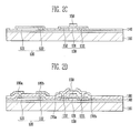
- FIGS. 2A-2D illustrate sequential cross-sectional views of a method for fabricating the light emitting display device 100 according to one exemplary embodiment of the present invention.
- the buffer layer 112 may be formed on the substrate 110.
- Patterned first and second polycrystalline silicon layers 120' and 130' may be formed on an upper surface of the buffer layer 112.
- the first and second polycrystalline silicon layers 120' and 130' may be spaced apart from each other.
- a single mask may be used to implant P-type impurities simultaneously into one side of the first polycrystalline silicon portion 120' and into two sides of the second polycrystalline silicon portion 130', as illustrated by the shadowed portions in FIG. 2B .
- Doping of the one side of the first polycrystalline silicon portion 120' with P-type impurities may form the P-type doping region 122.
- Doping of both sides of the second polycrystalline silicon portion 130' with P-type impurities may form the source/drain regions 132 and 133.
- the undoped portions of the first and second polycrystalline silicon portions 120' and 130' may be formed into the intrinsic region 121 of the PD120 and the intrinsic region 131 of the semiconductor layer 130, respectively.
- the first polycrystalline silicon portion 120' may be formed into the PD 120, and the second polycrystalline silicon portion 130' may be formed into the semiconductor layer 130 of the TFT 190.
- the intrinsic region 131 of the semiconductor layer 130 may correspond to a channel region between the source and drain regions 132 and 133.
- the first dielectric layer 140 may be formed on the buffer layer 112 to cover the semiconductor layer 130 and the PD 120.
- the gate electrode 150 may be formed on the first dielectric layer 140 in a region corresponding to the intrinsic region 131 of the semiconductor layer 130, i.e., the gate electrode 150 may overlap the intrinsic region 131.
- the second dielectric layer 160 may be formed on the first dielectric layer 140 to cover the gate electrode 150. Then, the first and second dielectric layers 140 and 160 may be etched to form contact holes therethrough to expose portions of upper surfaces of the source/drain regions 132 and 133 of the semiconductor layer 130 and portions of upper surfaces of the P-type doping region 122 and the intrinsic region 121 of the PD 120.
- Source and drain electrodes 170a and 170b may be coupled via the contact holes to the source and drain regions 132 and 133, respectively.
- First and second electrodes 180a and 180b may be coupled via the contact holes to the intrinsic region 121 and the P-type doping region 122, respectively.
- the first electrode 180a and the second electrode 180b may be spaced apart from each other along the x-axis to form sufficient space for transmitting light into the intrinsic region 121. More specifically, as illustrated in FIG. 3 , a portion of the intrinsic region 121 of the PD 120 may be between the first electrode 180a and the second electrode 180b, and may have a predetermined surface area of an upper surface thereof to provide light transmittance.
- the intrinsic region 121 may have a predetermined length L, e.g., about 4 ⁇ m, and a predetermined width W, e.g., about 25,000 ⁇ m, to form an exposed surface area, so light may be incident on the upper surface of the intrinsic region 121 between the first and second electrodes 180a and 180b.
- the length L and width W of the intrinsic region 121 may be varied according to a size of the PD 120.
- FIG. 4 illustrates a graph comparing light sensitivity of a PIN PD and an MIP PD.
- X axis represents voltage (V) applied to the PD
- Y axis represents a reverse current (A) of the PD that is varied according to the voltage applied to the PD.
- Each PD was formed to have a length L of 4 ⁇ m and a width W of 25,000 ⁇ m.
- an external light of a PD is measured when a voltage of -0.5 to -2.0 (V) is applied to the PD.
- the sensitivity ratio refers to a dynamic difference between ON/OFF states of the reverse current.
- the sensitivity ratio refers to a difference between an OFF state, i.e., a reverse current through the PD when external luminance is 0 Lux, and an ON state, i.e., a reverse current through the PD when the external luminance is greater than 0 Lux at a substantially same voltage.
- An external luminance of 0 Lux refers to dark surroundings with substantially no light, and external luminance that is greater than 0 Lux was used as 1000 Lux.
- the PD was determined as having an increased sensitivity to light if a sensitivity ratio thereof was high. For example, a higher sensitivity ratio between the ON/OFF states of the reverse current indicated a higher sensitivity to light.
- the MIP PD exhibited a higher sensitivity ratio than the NIP PD, i.e., a higher reverse current ratio between the two curves indicated by the double-headed arrows in FIG. 4 . More specifically, as illustrated in FIG. 4 , a sensitivity ratio of the PIN PD at a voltage varying from about (-0.5) V to about (-2.0) V was about 1 - 1.5 orders (v/decade), while a sensitivity ratio of the MIP PD at a same voltage range was about 1.2 - 1.8 orders. As such the MIP PD may have a higher sensitivity ratio, i.e., by about 0.2 to about 0.5 orders. Here, 1 order represents 10 -1 (A), and 2 orders represent 10 -2 (A). Also, the MIP PD exhibited better accuracy in measuring ambient light due to its increased sensitivity to the light.
- a PD according to embodiments of the present invention may be advantageous in exhibiting a higher light sensitivity than a PIN diode. Therefore, ambient light may be measured by the PD with an increased accuracy.
- the MIP diode may have an excellent sensitivity to the light since it has a higher sensitivity ratio than the PIN diode.
- the sensitivity of the PD may be enhanced by forming the PD to have a MIP structure. Therefore, the luminance of the LED may be controlled according the external light by detecting ambient light of the light emitting display device more effectively using the PD.
- the fabrication process may be simplified by doping one side of the photo diode with P-type impurity used in the source/drain region of the semiconductor layer.
Landscapes
- Engineering & Computer Science (AREA)
- Microelectronics & Electronic Packaging (AREA)
- Physics & Mathematics (AREA)
- General Physics & Mathematics (AREA)
- Theoretical Computer Science (AREA)
- Electroluminescent Light Sources (AREA)
- Devices For Indicating Variable Information By Combining Individual Elements (AREA)
- Light Receiving Elements (AREA)
Abstract
Description
- The present invention relates to a light emitting display device and a method of fabricating the same. More particularly, embodiments of the present invention relate to a light emitting display device with a photo diode and to a method of fabricating the same.
- A light emitting display device may include a light emitting diode (LED) that emits visible light to display images. The LED, however, may have high power consumption due to a constant luminance value thereof regardless of changes in ambient light. Therefore, attempts have been made to use a photo diode (PD) to control luminance of the LED. The PD may convert light energy, e.g., light emitted from the LED or ambient light, into an electrical signal, e.g., electric current or voltage, by generating electrons or holes in accordance with an optical absorption, e.g., intensity of light.
- The conventional PD in the light emitting display device, however, may include an intrinsic region between a region doped with P-type impurities and a region doped with N-type impurities, i.e., a PIN structure. Use of both P-type and N-type impurities in the PD may require use of multiple masks to form the PD. Further, additional masks may be required to form both the PD and a thin film transistor (TFT) of the light emitting display device with both P-type and N-type impurities. Accordingly, manufacturing costs and processes of the light emitting display device may be increased.
- Embodiments of the present invention are therefore directed to a light emitting display device and a method of fabricating the same, which substantially overcome one or more of the disadvantages and shortcomings of the related art.
- It is therefore a feature of an embodiment of the present invention to provide a light emitting display device with a PD having a simplified structure.
- It is therefore another feature of an embodiment of the present invention to provide a light emitting display device with a PD having increased light sensitivity.
- It is yet another feature of an embodiment of the present invention to provide a method of fabricating a light emitting display device with a PD having one or more of the above features.
- At least one of the above and other features and advantages of the present invention may be realized by providing a light emitting display device, including a light emitting diode and a thin film transistor on a substrate, the light emitting diode and thin film transistor being electrically coupled to each other; and a photo diode on the substrate, the photo diode including an intrinsic region and a P-type doping region coupled to each other. The light emitting display device may further include a first metal electrode coupled to the intrinsic region of the photo diode and a second metal electrode coupled to the P-type doping region of the photo diode, the first and second metal electrodes having a space therebetween.
- According to an aspect of the invention, the PD does not include an N-Type doping region. In other words, the PD comprises an intrinsic region and a single impurity type doping region, being a P-type doping region.
- An upper surface of the intrinsic region of the photo diode may overlap the space between the first and second metal electrodes. The thin film transistor may be a PMOS. The photo diode may be spaced apart from the thin film transistor. The photo diode and the thin film transistor may be co-planar along a plane parallel to a plane of the substrate. The P-type doping region and the intrinsic region of the photo diode may be co-planar along a plane parallel to a plane of the substrate. The P-type doping region may be between the thin film transistor and the intrinsic region. The light emitting display device may further include a controller, the controller being configured to control voltage applied to the light emitting diode in accordance with an electrical signal output from the photo diode. The photo diode may consist essentially of the P-type doping region and the intrinsic region.
- At least one of the above and other features and advantages of the present invention may be also realized by providing a method of fabricating a light emitting display device, including forming a thin film transistor on a substrate, forming a photo diode on the substrate, the photo diode including an intrinsic region and a P-type doping region coupled to each other, and forming a light emitting diode on the substrate, such that the light emitting diode and the thin film transistor are electrically coupled to each other.
- Forming the photo diode and the thin film transistor on the substrate may include disposing a first polycrystalline silicon layer and a second polycrystalline silicon layer, respectively, on the substrate. The first and second polycrystalline silicon layers may be co-planar. Forming the photo diode and the thin film transistor on the substrate may further include doping one side of the first polycrystalline silicon layer and both sides of the second polycrystalline silicon layer with P-type impurities to form a P-type doping region in one side of the first polycrystalline silicon layer and a source region and a drain region in the second polycrystalline silicon layer. Doping the first and second polycrystalline silicon layers may include using a single mask. Doping of the first and second polycrystalline silicon layers may be simultaneous. The method may further include stacking a first dielectric layer and a second dielectric layer on the substrate to cover the first polycrystalline silicon layer and the second polycrystalline silicon layer. The method may further include forming contact holes through the first and second dielectric layers, such that first and second electrodes are coupled to the photo diode through the contact holes and source and drain electrodes are coupled to the thin film transistor through the contact holes.
- The above and other features and advantages of the present invention will become more apparent to those of ordinary skill in the art by describing in detail exemplary embodiments thereof with reference to the attached drawings, in which:
-
FIG. 1 illustrates a partial cross-sectional view of a light emitting display device according to an exemplary embodiment of the present invention; -
FIGS. 2A-2D illustrate sequential cross-sectional views of a method for fabricating a light emitting display device according to an exemplary embodiment of the present invention; -
FIG. 3 illustrates a perspective view of a PD according to an exemplary embodiment of the present invention; and -
FIG. 4 illustrates a graph comparing light sensitivity of a conventional PD and a PD according to an exemplary embodiment of the present invention. - Embodiments of the present invention will now be described more fully hereinafter with reference to the accompanying drawings, in which exemplary embodiments of the invention are illustrated. Aspects of the invention may, however, be embodied in different forms and should not be construed as limited to the embodiments set forth herein. Rather, these embodiments are provided so that this disclosure will be thorough and complete, and will fully convey the scope of the invention to those skilled in the art.
- In the figures, the dimensions of layers, elements, and regions may be exaggerated for clarity of illustration. It will also be understood that when a layer or element is referred to as being "on" another layer, element, or substrate, it can be directly on the other layer, element, or substrate, or intervening layers and/or elements may also be present. Further, it will be understood that the term "on" can indicate solely a vertical arrangement of one element with respect to another element, and may not indicate a vertical orientation, e.g., a horizontal orientation. In addition, it will be understood that when a layer or element is referred to as being "under" another layer or element, it can be directly under, or one or more intervening layers and/or elements may also be present. Further, it will also be understood that when a layer or element is referred to as being "between" two layers or elements, it can be the only layer or element between the two layers or elements, or one or more intervening layers and/or elements may also be present. Like reference numerals refer to like elements throughout.
- As used herein, the expressions "at least one," "one or more," and "and/or" are open-ended expressions that are both conjunctive and disjunctive in operation. For example, each of the expressions "at least one of A, B, and C," "at least one of A, B, or C," "one or more of A, B, and C," "one or more of A, B, or C" and "A, B, and/or C" includes the following meanings: A alone; B alone; C alone; both A and B together; both A and C together; both B and C together; and all three of A, B, and C together. Further, these expressions are open-ended, unless expressly designated to the contrary by their combination with the term "consisting of." For example, the expression "at least one of A, B, and C" may also include an nth member, where n is greater than 3, whereas the expression "at least one selected from the group consisting of A, B, and C" does not.
-
FIG. 1 illustrates a cross-sectional view of a light emitting display device according to one exemplary embodiment of the present invention. Referring toFIG. 1 , a lightemitting display device 100 may include a TFT 190 and aPD 120 on asubstrate 110. The lightemitting display device 100 may further include an LED (not shown), e.g., an organic light emitting diode (OLED), on thesubstrate 110. - The TFT 190 may include a
semiconductor layer 130, agate electrode 150, and source/drain electrodes semiconductor layer 130 of the TFT 190 may include asource region 132, adrain region 133, and anintrinsic region 131 between thesource region 132 and thedrain region 133. Both thesource region 132 and thedrain region 133 of thesemiconductor layer 130 may be doped with impurity having substantially the same conductivity. For example, both the source anddrain regions drain regions semiconductor layer 130, so formation of a PMOS may require a lower number of masks than, e.g., a CMOS. Accordingly, productivity and yield of the lightemitting display device 100 may be improved. - A
buffer layer 112 may be disposed between thesubstrate 110 and theTFT 190, so thesemiconductor layer 130 of theTFT 190 may be formed on thebuffer layer 112. A firstdielectric layer 140 may be formed on thebuffer layer 112 to cover thesemiconductor layer 130, i.e., thesemiconductor layer 130 may be between thebuffer layer 112 and the firstdielectric layer 140. Thegate electrode 150 may be formed on thefirst dielectric layer 140 in a region corresponding to theintrinsic region 131 of thesemiconductor layer 130. Asecond dielectric layer 160 may be formed on thefirst dielectric layer 140 to cover thegate electrode 150, i.e., thegate electrode 150 may be between the first and seconddielectric layers drain electrodes second dielectric layer 160, so thesource electrode 170a and thedrain electrode 170b may be coupled respectively to thesource region 132 and thedrain region 133 of thesemiconductor layer 130 through contact holes in the first and seconddielectric layers - The light emitting
display device 100 may further include a third dielectric layer (not shown) on theTFT 190, so the LED may be formed on the third dielectric layer. The LED may be electrically coupled to theTFT 190. The LED may be any suitable LED, e.g., an OLED. A controller may be connected to the LED for controlling luminance thereof in accordance with electrical signals, e.g., voltage signals, output by thePD 120. - The
PD 120 of the light emittingdisplay device 100 may be electrically coupled to the LED, and may control luminance of the LED. For example, thePD 120 may be between thesubstrate 110 and the LED in a non-light emission region of the light emittingdisplay device 100. In particular, thePD 120 may be on thebuffer layer 112, and may be spaced apart from theTFT 190 along the x-axis. More specifically, thesemiconductor layer 130 of theTFT 190 and thePD 120 may be co-planar along a plane parallel to thesubstrate 110, e.g., a horizontal plane along the x-axis. For example, both thesemiconductor layer 130 and thePD 120 may be directly on thebuffer layer 112. Further, thesemiconductor layer 130 and thePD 120 may be formed of substantially the same material, e.g., polycrystalline silicon. As such, formation of thePD 120 and thesemiconductor layer 130 may be substantially simplified by depositing two polycrystalline silicon layers spaced apart from each on the same plane, e.g., simultaneously. - The
PD 120 may include a single impurity region having substantially the same conductivity as the source and drainregions semiconductor layer 133. For example, thePD 120 may include a P-type impurity region. More specifically, thePD 120 may include a P-type doping region 122, anintrinsic region 121, and first andsecond electrodes intrinsic region 121 and the P-type doping region 122, respectively. The first andsecond electrodes PD 120 may have a metal intrinsic P+ (MIP) structure. In the MIP structure, M represents the first andsecond electrodes intrinsic region 121, and P represents the P-type doping region 122. - The P-
type doping region 122 and theintrinsic region 121 may be coplanar along a plane parallel to thesubstrate 110, and may be coupled to each other. More specifically, one side of the polycrystalline silicon layer of thePD 120 may be doped with P-type impurities simultaneously with the polycrystalline silicon layer ofsemiconductor layer 130 to form the P-type doping region 122. A side of the polycrystalline silicon layer of thePD 120 not doped with P-type impurities may define theintrinsic region 121. - The P-
type doping region 122 of thePD 120 may be formed on thebuffer layer 112, and may be on a side of thePD 120 adjacent to thesemiconductor layer 130 of theTFT 190. More specifically, the P-type doping region 122 may be between theintrinsic region 121 and theTFT 190. Therefore, the P-type doping region 122 of thePD 120 may not require a separate mask for implanting P-type impurity therein, i.e., may be formed via a same mask used to form the doping regions of thesemiconductor layer 130. Theintrinsic region 121 may be on thebuffer layer 112 and in direct contact with the P-type doping region 122. Therefore, the thickness of the light emittingdisplay device 100 may be minimized due to a horizontal structure of thePD 120, i.e., the P-type doping region 122 and theintrinsic region 121 being on substantially the same plane. The first and seconddielectric layers PD 120, so the first andsecond electrodes intrinsic region 121 and the P-type doping region 122, respectively, via contact holes in the first and seconddielectric layers - The
PD 120 may be a semiconductor device for converting an optical signal into an electrical signal, and its driving method is as follows. When a negative (-) voltage is applied to the P-type doping region 122 through thesecond electrode 180b and a positive (+) voltage is applied to theintrinsic region 121 through thefirst electrode 180a simultaneously, thePD 120 may generate electrons and holes in theintrinsic region 121 in accordance with light incident on theintrinsic region 121. Current may flow in the intrinsic region 123 by means of a reverse electric field. - The
PD 120 according to embodiments of the present invention may include only a P-type doping region, i.e., may not include a N-type doping region, so the number of doping stages and masks may be reduced, thereby simplifying a manufacturing process of thePD 120. Also, thePD 120 may be formed to have a MIP structure, so light sensitivity of thePD 120 may be higher as compared, e.g., to a PD having a PIN structure, and therefore, thePD 120 may have an increased efficiency in controlling luminance of the LED. A comparison between thePD 120 and a PD having a PIN structure will be explained in more detail below with reference toFIG. 4 . It is noted that a PD having a PIN structure refers to a PD having a P-type doping region, an N-type doping region, and an intrinsic region between the P-type doping region and the N-type doping region. - Accordingly, a light emitting display device formed according to embodiments of the present invention may have reduced power consumption of its LED due to improved luminance control thereof via the PD. In addition, ambient light, i.e., light external to the light emitting
display device 100, may be measured with improved accuraacy due to improved light sensitivity of thePD 120, thereby providing improved display properties of the light emittingdisplay device 100.
FIGS. 2A-2D illustrate sequential cross-sectional views of a method for fabricating the light emittingdisplay device 100 according to one exemplary embodiment of the present invention. - Referring to
FIG. 2A , thebuffer layer 112 may be formed on thesubstrate 110. Patterned first and second polycrystalline silicon layers 120' and 130' may be formed on an upper surface of thebuffer layer 112. The first and second polycrystalline silicon layers 120' and 130' may be spaced apart from each other. - Referring to
FIG. 2B , a single mask (not shown) may be used to implant P-type impurities simultaneously into one side of the first polycrystalline silicon portion 120' and into two sides of the second polycrystalline silicon portion 130', as illustrated by the shadowed portions inFIG. 2B . Doping of the one side of the first polycrystalline silicon portion 120' with P-type impurities may form the P-type doping region 122. Doping of both sides of the second polycrystalline silicon portion 130' with P-type impurities may form the source/drain regions intrinsic region 121 of the PD120 and theintrinsic region 131 of thesemiconductor layer 130, respectively. Therefore, the first polycrystalline silicon portion 120' may be formed into thePD 120, and the second polycrystalline silicon portion 130' may be formed into thesemiconductor layer 130 of theTFT 190. Theintrinsic region 131 of thesemiconductor layer 130 may correspond to a channel region between the source and drainregions FIG. 2C , thefirst dielectric layer 140 may be formed on thebuffer layer 112 to cover thesemiconductor layer 130 and thePD 120. Also, thegate electrode 150 may be formed on thefirst dielectric layer 140 in a region corresponding to theintrinsic region 131 of thesemiconductor layer 130, i.e., thegate electrode 150 may overlap theintrinsic region 131. - Referring to
FIG. 2D , thesecond dielectric layer 160 may be formed on thefirst dielectric layer 140 to cover thegate electrode 150. Then, the first and seconddielectric layers drain regions semiconductor layer 130 and portions of upper surfaces of the P-type doping region 122 and theintrinsic region 121 of thePD 120. Source anddrain electrodes regions second electrodes intrinsic region 121 and the P-type doping region 122, respectively. - The
first electrode 180a and thesecond electrode 180b may be spaced apart from each other along the x-axis to form sufficient space for transmitting light into theintrinsic region 121. More specifically, as illustrated inFIG. 3 , a portion of theintrinsic region 121 of thePD 120 may be between thefirst electrode 180a and thesecond electrode 180b, and may have a predetermined surface area of an upper surface thereof to provide light transmittance. For example, theintrinsic region 121 may have a predetermined length L, e.g., about 4 µm, and a predetermined width W, e.g., about 25,000 µm, to form an exposed surface area, so light may be incident on the upper surface of theintrinsic region 121 between the first andsecond electrodes intrinsic region 121 may be varied according to a size of thePD 120. -
FIG. 4 illustrates a graph comparing light sensitivity of a PIN PD and an MIP PD. InFIG. 4 , X axis represents voltage (V) applied to the PD, and Y axis represents a reverse current (A) of the PD that is varied according to the voltage applied to the PD. Each PD was formed to have a length L of 4 µm and a width W of 25,000 µm. Generally, an external light of a PD is measured when a voltage of -0.5 to -2.0 (V) is applied to the PD. - A voltage of -5 to 0 (V) was applied to each PD, and a reverse current of the PD was measured when the voltage on the PD was varied between -5 V to 0 V. Ambient light was measured by each PD. In order to determine sensitivity of each of the PDs to light, a sensitivity ratio was measured. The sensitivity ratio refers to a dynamic difference between ON/OFF states of the reverse current. In other words, the sensitivity ratio refers to a difference between an OFF state, i.e., a reverse current through the PD when external luminance is 0 Lux, and an ON state, i.e., a reverse current through the PD when the external luminance is greater than 0 Lux at a substantially same voltage. An external luminance of 0 Lux refers to dark surroundings with substantially no light, and external luminance that is greater than 0 Lux was used as 1000 Lux. The PD was determined as having an increased sensitivity to light if a sensitivity ratio thereof was high. For example, a higher sensitivity ratio between the ON/OFF states of the reverse current indicated a higher sensitivity to light.
- As illustrated in
FIG. 4 , the MIP PD exhibited a higher sensitivity ratio than the NIP PD, i.e., a higher reverse current ratio between the two curves indicated by the double-headed arrows inFIG. 4 . More specifically, as illustrated inFIG. 4 , a sensitivity ratio of the PIN PD at a voltage varying from about (-0.5) V to about (-2.0) V was about 1 - 1.5 orders (v/decade), while a sensitivity ratio of the MIP PD at a same voltage range was about 1.2 - 1.8 orders. As such the MIP PD may have a higher sensitivity ratio, i.e., by about 0.2 to about 0.5 orders. Here, 1 order represents 10-1 (A), and 2 orders represent 10-2 (A). Also, the MIP PD exhibited better accuracy in measuring ambient light due to its increased sensitivity to the light. - A PD according to embodiments of the present invention, e.g., a MIP diode, may be advantageous in exhibiting a higher light sensitivity than a PIN diode. Therefore, ambient light may be measured by the PD with an increased accuracy. As a result, the MIP diode may have an excellent sensitivity to the light since it has a higher sensitivity ratio than the PIN diode. More specifically, the sensitivity of the PD may be enhanced by forming the PD to have a MIP structure. Therefore, the luminance of the LED may be controlled according the external light by detecting ambient light of the light emitting display device more effectively using the PD. Also, the fabrication process may be simplified by doping one side of the photo diode with P-type impurity used in the source/drain region of the semiconductor layer.
- Exemplary embodiments of the present invention have been disclosed herein, and although specific terms are employed, they are used and are to be interpreted in a generic and descriptive sense only and not for purpose of limitation. Accordingly, it will be understood by those of ordinary skill in the art that various changes in form and details may be made without departing from the scope of the present invention as set forth in the following claims.
Claims (17)
- A light emitting display device, comprising:a light emitting diode and a thin film transistor on a substrate, the light emitting diode and thin film transistor being electrically coupled to each other; anda photo diode on the substrate, the photo diode including an intrinsic region and a P-type doping region coupled to each other,wherein the photo diode does not include an N-type doping region.
- The light emitting display device as claimed in claim 1, further comprising a first metal electrode coupled to the intrinsic region of the photo diode and a second metal electrode coupled to the P-type doping region of the photo diode, the first and second metal electrodes having a space therebetween.
- The light emitting display device as claimed in claim 2, wherein an upper surface of the intrinsic region of the photo diode overlaps the space between the first and second metal electrodes.
- The light emitting display device as claimed in any one of the preceding claims, wherein the thin film transistor is a PMOS.
- The light emitting display device as claimed in any one of the preceding claims, wherein the photo diode is spaced apart from the thin film transistor.
- The light emitting display device as claimed in claim 5, wherein the photo diode and the thin film transistor are co-planar along a plane parallel to a plane of the substrate.
- The light emitting display device as claimed in claim 5 or 6, wherein the P-type doping region and the intrinsic region of the photo diode are co-planar along a plane parallel to a plane of the substrate.
- The light emitting display device as claimed in claim 7, wherein the P-type doping region is between the thin film transistor and the intrinsic region.
- The light emitting display device as claimed in any one of the preceding claims, wherein the photo diode consists essentially of the P-type doping region and the intrinsic region.
- A method of fabricating a light emitting display device, comprising:forming a thin film transistor on a substrate,forming a photo diode on the substrate, the photo diode including an intrinsic region and a P-type doping region coupled to each other, but not including an N-type doping region; andforming a light emitting diode on the substrate, such that the light emitting diode and the thin film transistor are electrically coupled to each other.
- The method as claimed in claim 10, wherein forming the photo diode and the thin film transistor on the substrate includes disposing a first polycrystalline silicon layer and a second polycrystalline silicon layer, respectively, on the substrate.
- The method as claimed in claim 11, wherein the first and second polycrystalline silicon layers are co-planar.
- The method as claimed in claim 11, wherein forming the photo diode and the thin film transistor on the substrate further comprises doping one side of the first polycrystalline silicon layer and both sides of the second polycrystalline silicon layer with P-type impurities to form a P-type doping region in one side of the first polycrystalline silicon layer and a source region and a drain region in the second polycrystalline silicon layer.
- The method as claimed in claim 13, wherein doping the first and second polycrystalline silicon layers includes using a single mask.
- The method as claimed in claim 13, wherein doping of the first and second polycrystalline silicon layers is simultaneous.
- The method as claimed in claim 13, 14 or 15, further comprising stacking a first dielectric layer and a second dielectric layer on the substrate to cover the first polycrystalline silicon layer and the second polycrystalline silicon layer.
- The method as claimed in claim 16, further comprising forming contact holes through the first and second dielectric layers, such that first and second electrodes are coupled to the photo diode through the contact holes and source and drain electrodes are coupled to the thin film transistor through the contact holes.
Applications Claiming Priority (1)
| Application Number | Priority Date | Filing Date | Title |
|---|---|---|---|
| KR1020070093633A KR100882693B1 (en) | 2007-09-14 | 2007-09-14 | Light emitting display device and manufacturing method thereof |
Publications (2)
| Publication Number | Publication Date |
|---|---|
| EP2037502A2 true EP2037502A2 (en) | 2009-03-18 |
| EP2037502A3 EP2037502A3 (en) | 2012-10-10 |
Family
ID=40130582
Family Applications (1)
| Application Number | Title | Priority Date | Filing Date |
|---|---|---|---|
| EP08164168A Withdrawn EP2037502A3 (en) | 2007-09-14 | 2008-09-11 | Light emitting display device and method of fabricating the same |
Country Status (5)
| Country | Link |
|---|---|
| US (1) | US7816684B2 (en) |
| EP (1) | EP2037502A3 (en) |
| JP (1) | JP4528323B2 (en) |
| KR (1) | KR100882693B1 (en) |
| CN (1) | CN101388405B (en) |
Families Citing this family (4)
| Publication number | Priority date | Publication date | Assignee | Title |
|---|---|---|---|---|
| US9311860B2 (en) | 2013-09-06 | 2016-04-12 | Lenovo Enterprise Solutions (Singapore) Pte. Ltd. | Liquid crystal display using backlight intensity to compensate for pixel damage |
| KR102265752B1 (en) * | 2014-09-01 | 2021-06-17 | 삼성디스플레이 주식회사 | organic light emitting diode display |
| CN109087928B (en) * | 2018-08-16 | 2021-01-26 | 京东方科技集团股份有限公司 | Photoelectric detection substrate, preparation method thereof and photoelectric detection device |
| CN110071164B (en) * | 2019-05-07 | 2021-05-04 | 京东方科技集团股份有限公司 | A display substrate, a brightness adjustment method thereof, and a display device |
Citations (4)
| Publication number | Priority date | Publication date | Assignee | Title |
|---|---|---|---|---|
| JP2001085160A (en) * | 1999-09-20 | 2001-03-30 | Nec Corp | Light-emitting element with emission output correction function |
| JP2002237923A (en) | 2001-02-09 | 2002-08-23 | Nec Corp | Image input device with built-in display function |
| WO2004109641A1 (en) | 2003-06-11 | 2004-12-16 | Koninklijke Philips Electronics N.V. | Colour electroluminescent display devices |
| EP1801883A1 (en) | 2005-12-21 | 2007-06-27 | Samsung SDI Co., Ltd. | Photo sensor and organic light-emitting display using the same |
Family Cites Families (29)
| Publication number | Priority date | Publication date | Assignee | Title |
|---|---|---|---|---|
| US5225706A (en) | 1987-12-04 | 1993-07-06 | Thomson-Csf | Matrix of photosensitive elements associating a photodiode or a phototransistor and a storage capacitor |
| FR2624306B1 (en) * | 1987-12-04 | 1990-04-20 | Thomson Csf | MATRIX OF PHOTOSENSITIVE ELEMENTS COMBINING A PHOTODIODE OR A PHOTOTRANSISTOR AND A STORAGE CAPACITY |
| KR19990012529A (en) * | 1997-07-29 | 1999-02-25 | 윤종용 | Light emitting display device and control method |
| TW480727B (en) * | 2000-01-11 | 2002-03-21 | Semiconductor Energy Laboratro | Semiconductor display device |
| WO2001084561A2 (en) * | 2000-05-04 | 2001-11-08 | E.I. Du Pont De Nemours And Company | Tunable devices incorporating bicu3ti3feo¿12? |
| JP2002072963A (en) | 2000-06-12 | 2002-03-12 | Semiconductor Energy Lab Co Ltd | Light emitting module, driving method thereof, and optical sensor |
| JP3975391B2 (en) * | 2001-03-15 | 2007-09-12 | セイコーエプソン株式会社 | Semiconductor device, image sensor, PIN diode, and electronic device |
| JP2002368254A (en) | 2001-06-04 | 2002-12-20 | Mitsubishi Cable Ind Ltd | Semiconductor light-receiving element and manufacturing method therefor |
| JP2005019353A (en) | 2003-06-30 | 2005-01-20 | Sanyo Electric Co Ltd | El display device and its manufacturing method |
| JP4219755B2 (en) | 2003-07-16 | 2009-02-04 | ローム株式会社 | Image sensor manufacturing method and image sensor |
| JP2005116681A (en) | 2003-10-06 | 2005-04-28 | Toshiba Corp | Optical semiconductor light-receiving element and manufacturing method thereof |
| US20050200291A1 (en) | 2004-02-24 | 2005-09-15 | Naugler W. E.Jr. | Method and device for reading display pixel emission and ambient luminance levels |
| US20060007248A1 (en) | 2004-06-29 | 2006-01-12 | Damoder Reddy | Feedback control system and method for operating a high-performance stabilized active-matrix emissive display |
| US20050200294A1 (en) | 2004-02-24 | 2005-09-15 | Naugler W. E.Jr. | Sidelight illuminated flat panel display and touch panel input device |
| US20050200292A1 (en) | 2004-02-24 | 2005-09-15 | Naugler W. E.Jr. | Emissive display device having sensing for luminance stabilization and user light or touch screen input |
| EP1723397A2 (en) | 2004-02-24 | 2006-11-22 | Nuelight Corporation | Penlight and touch screen data input system and method for flat panel displays |
| US20050200296A1 (en) | 2004-02-24 | 2005-09-15 | Naugler W. E.Jr. | Method and device for flat panel emissive display using shielded or partially shielded sensors to detect user screen inputs |
| KR100984362B1 (en) * | 2004-04-02 | 2010-09-30 | 삼성전자주식회사 | Organic electro-luminescence panel |
| KR20050121090A (en) | 2004-06-21 | 2005-12-26 | (주)아이씨선 | Semiconductor equipment having finger type diffusion layer and manufacture method thereof |
| JP2006030317A (en) * | 2004-07-12 | 2006-02-02 | Sanyo Electric Co Ltd | Organic el display device |
| KR101080354B1 (en) * | 2004-08-12 | 2011-11-04 | 삼성전자주식회사 | Thin film transistor array panel and manufacturing method thereof |
| KR101100880B1 (en) * | 2004-09-24 | 2012-01-02 | 삼성전자주식회사 | Manufacturing Method of Flexible Display |
| KR101143005B1 (en) * | 2004-12-14 | 2012-05-08 | 삼성전자주식회사 | Mask and method for manufacturing semiconductor device and thin film transistor array panel using the mask |
| KR101112549B1 (en) * | 2005-01-31 | 2012-06-12 | 삼성전자주식회사 | Thin film transistor array panel |
| JP4931367B2 (en) * | 2005-04-28 | 2012-05-16 | シャープ株式会社 | Detection device and display device having the same |
| KR100759681B1 (en) | 2006-03-29 | 2007-09-17 | 삼성에스디아이 주식회사 | Organic electroluminescent display |
| KR100759689B1 (en) * | 2006-04-18 | 2007-09-17 | 삼성에스디아이 주식회사 | Organic electroluminescent display |
| KR100840099B1 (en) * | 2007-07-04 | 2008-06-19 | 삼성에스디아이 주식회사 | Manufacturing method of organic electroluminescent device provided with photo diamond |
| KR100882679B1 (en) * | 2007-09-14 | 2009-02-06 | 삼성모바일디스플레이주식회사 | Light emitting display device and manufacturing method thereof |
-
2007
- 2007-09-14 KR KR1020070093633A patent/KR100882693B1/en not_active Expired - Fee Related
- 2007-11-02 JP JP2007286522A patent/JP4528323B2/en not_active Expired - Fee Related
-
2008
- 2008-06-24 US US12/213,736 patent/US7816684B2/en active Active
- 2008-09-03 CN CN200810215141XA patent/CN101388405B/en active Active
- 2008-09-11 EP EP08164168A patent/EP2037502A3/en not_active Withdrawn
Patent Citations (4)
| Publication number | Priority date | Publication date | Assignee | Title |
|---|---|---|---|---|
| JP2001085160A (en) * | 1999-09-20 | 2001-03-30 | Nec Corp | Light-emitting element with emission output correction function |
| JP2002237923A (en) | 2001-02-09 | 2002-08-23 | Nec Corp | Image input device with built-in display function |
| WO2004109641A1 (en) | 2003-06-11 | 2004-12-16 | Koninklijke Philips Electronics N.V. | Colour electroluminescent display devices |
| EP1801883A1 (en) | 2005-12-21 | 2007-06-27 | Samsung SDI Co., Ltd. | Photo sensor and organic light-emitting display using the same |
Also Published As
| Publication number | Publication date |
|---|---|
| EP2037502A3 (en) | 2012-10-10 |
| CN101388405B (en) | 2011-06-15 |
| JP4528323B2 (en) | 2010-08-18 |
| CN101388405A (en) | 2009-03-18 |
| KR100882693B1 (en) | 2009-02-06 |
| US7816684B2 (en) | 2010-10-19 |
| US20090072247A1 (en) | 2009-03-19 |
| JP2009069791A (en) | 2009-04-02 |
Similar Documents
| Publication | Publication Date | Title |
|---|---|---|
| KR100840098B1 (en) | Organic electroluminescent device and manufacturing method thereof | |
| TWI394071B (en) | Oled touch panel and method of forming the same | |
| JP6305095B2 (en) | Graphene element and electronic device including the same | |
| US8477125B2 (en) | Photo sensor and organic light-emitting display using the same | |
| US20160293586A1 (en) | Method of integrating inorganic light emitting diode with oxide thin film transistor for display applications | |
| JP2007300064A (en) | Organic electroluminescent display device and manufacturing method thereof | |
| EP1865560B1 (en) | Organic light-emitting display device | |
| KR100684675B1 (en) | Optical sensors and displays | |
| CN100511702C (en) | Organic light-emitting display device | |
| CN109155328B (en) | Display substrate, display panel, display apparatus, and method of manufacturing display substrate | |
| US7915649B2 (en) | Light emitting display device and method of fabricating the same | |
| US8022622B2 (en) | Organic light-emitting display device including a photo diode | |
| US7816684B2 (en) | Light emitting display device and method of fabricating the same | |
| US8076669B2 (en) | Organic light emitting display and method of manufacturing the same | |
| US7642547B2 (en) | Light emitting device and method of manufacturing the same | |
| US7687870B2 (en) | Laterally configured electrooptical devices | |
| US20240243216A1 (en) | Light sensing device and method of manufacturing the same, image sensor including light sensing device, and electronic apparatus including image sensor | |
| TW202533702A (en) | Transistor and display device including the same | |
| US20210050479A1 (en) | Micro light emitting diode and micro light emitting diode device substrate |
Legal Events
| Date | Code | Title | Description |
|---|---|---|---|
| PUAI | Public reference made under article 153(3) epc to a published international application that has entered the european phase |
Free format text: ORIGINAL CODE: 0009012 |
|
| 17P | Request for examination filed |
Effective date: 20080911 |
|
| AK | Designated contracting states |
Kind code of ref document: A2 Designated state(s): AT BE BG CH CY CZ DE DK EE ES FI FR GB GR HR HU IE IS IT LI LT LU LV MC MT NL NO PL PT RO SE SI SK TR |
|
| AX | Request for extension of the european patent |
Extension state: AL BA MK RS |
|
| RAP1 | Party data changed (applicant data changed or rights of an application transferred) |
Owner name: SAMSUNG MOBILE DISPLAY CO., LTD. |
|
| PUAL | Search report despatched |
Free format text: ORIGINAL CODE: 0009013 |
|
| RAP1 | Party data changed (applicant data changed or rights of an application transferred) |
Owner name: SAMSUNG DISPLAY CO., LTD. |
|
| AK | Designated contracting states |
Kind code of ref document: A3 Designated state(s): AT BE BG CH CY CZ DE DK EE ES FI FR GB GR HR HU IE IS IT LI LT LU LV MC MT NL NO PL PT RO SE SI SK TR |
|
| AX | Request for extension of the european patent |
Extension state: AL BA MK RS |
|
| RIC1 | Information provided on ipc code assigned before grant |
Ipc: H01L 27/32 20060101AFI20120905BHEP |
|
| 17Q | First examination report despatched |
Effective date: 20120927 |
|
| AKX | Designation fees paid |
Designated state(s): DE FR GB HU |
|
| RAP1 | Party data changed (applicant data changed or rights of an application transferred) |
Owner name: SAMSUNG DISPLAY CO., LTD. |
|
| STAA | Information on the status of an ep patent application or granted ep patent |
Free format text: STATUS: EXAMINATION IS IN PROGRESS |
|
| STAA | Information on the status of an ep patent application or granted ep patent |
Free format text: STATUS: THE APPLICATION IS DEEMED TO BE WITHDRAWN |
|
| 18D | Application deemed to be withdrawn |
Effective date: 20190719 |