EP2033247B1 - Thin film battery on an integrated circuit or circuit board and method thereof - Google Patents
Thin film battery on an integrated circuit or circuit board and method thereof Download PDFInfo
- Publication number
- EP2033247B1 EP2033247B1 EP07797463.2A EP07797463A EP2033247B1 EP 2033247 B1 EP2033247 B1 EP 2033247B1 EP 07797463 A EP07797463 A EP 07797463A EP 2033247 B1 EP2033247 B1 EP 2033247B1
- Authority
- EP
- European Patent Office
- Prior art keywords
- battery
- conductive
- circuit board
- printed circuit
- semiconductor device
- Prior art date
- Legal status (The legal status is an assumption and is not a legal conclusion. Google has not performed a legal analysis and makes no representation as to the accuracy of the status listed.)
- Active
Links
Images


Classifications
-
- H—ELECTRICITY
- H01—ELECTRIC ELEMENTS
- H01M—PROCESSES OR MEANS, e.g. BATTERIES, FOR THE DIRECT CONVERSION OF CHEMICAL ENERGY INTO ELECTRICAL ENERGY
- H01M10/00—Secondary cells; Manufacture thereof
- H01M10/05—Accumulators with non-aqueous electrolyte
- H01M10/058—Construction or manufacture
- H01M10/0585—Construction or manufacture of accumulators having only flat construction elements, i.e. flat positive electrodes, flat negative electrodes and flat separators
-
- H—ELECTRICITY
- H01—ELECTRIC ELEMENTS
- H01M—PROCESSES OR MEANS, e.g. BATTERIES, FOR THE DIRECT CONVERSION OF CHEMICAL ENERGY INTO ELECTRICAL ENERGY
- H01M50/00—Constructional details or processes of manufacture of the non-active parts of electrochemical cells other than fuel cells, e.g. hybrid cells
- H01M50/50—Current conducting connections for cells or batteries
- H01M50/531—Electrode connections inside a battery casing
- H01M50/533—Electrode connections inside a battery casing characterised by the shape of the leads or tabs
-
- H—ELECTRICITY
- H10—SEMICONDUCTOR DEVICES; ELECTRIC SOLID-STATE DEVICES NOT OTHERWISE PROVIDED FOR
- H10W—GENERIC PACKAGES, INTERCONNECTIONS, CONNECTORS OR OTHER CONSTRUCTIONAL DETAILS OF DEVICES COVERED BY CLASS H10
- H10W42/00—Arrangements for protection of devices
-
- H—ELECTRICITY
- H01—ELECTRIC ELEMENTS
- H01M—PROCESSES OR MEANS, e.g. BATTERIES, FOR THE DIRECT CONVERSION OF CHEMICAL ENERGY INTO ELECTRICAL ENERGY
- H01M10/00—Secondary cells; Manufacture thereof
- H01M10/04—Construction or manufacture in general
- H01M10/0436—Small-sized flat cells or batteries for portable equipment
-
- H—ELECTRICITY
- H01—ELECTRIC ELEMENTS
- H01M—PROCESSES OR MEANS, e.g. BATTERIES, FOR THE DIRECT CONVERSION OF CHEMICAL ENERGY INTO ELECTRICAL ENERGY
- H01M10/00—Secondary cells; Manufacture thereof
- H01M10/05—Accumulators with non-aqueous electrolyte
- H01M10/052—Li-accumulators
-
- H—ELECTRICITY
- H01—ELECTRIC ELEMENTS
- H01M—PROCESSES OR MEANS, e.g. BATTERIES, FOR THE DIRECT CONVERSION OF CHEMICAL ENERGY INTO ELECTRICAL ENERGY
- H01M10/00—Secondary cells; Manufacture thereof
- H01M10/05—Accumulators with non-aqueous electrolyte
- H01M10/056—Accumulators with non-aqueous electrolyte characterised by the materials used as electrolytes, e.g. mixed inorganic/organic electrolytes
- H01M10/0561—Accumulators with non-aqueous electrolyte characterised by the materials used as electrolytes, e.g. mixed inorganic/organic electrolytes the electrolyte being constituted of inorganic materials only
- H01M10/0562—Solid materials
-
- H—ELECTRICITY
- H01—ELECTRIC ELEMENTS
- H01M—PROCESSES OR MEANS, e.g. BATTERIES, FOR THE DIRECT CONVERSION OF CHEMICAL ENERGY INTO ELECTRICAL ENERGY
- H01M4/00—Electrodes
- H01M4/02—Electrodes composed of, or comprising, active material
- H01M4/04—Processes of manufacture in general
-
- H—ELECTRICITY
- H01—ELECTRIC ELEMENTS
- H01M—PROCESSES OR MEANS, e.g. BATTERIES, FOR THE DIRECT CONVERSION OF CHEMICAL ENERGY INTO ELECTRICAL ENERGY
- H01M4/00—Electrodes
- H01M4/02—Electrodes composed of, or comprising, active material
- H01M4/13—Electrodes for accumulators with non-aqueous electrolyte, e.g. for lithium-accumulators; Processes of manufacture thereof
- H01M4/139—Processes of manufacture
-
- H—ELECTRICITY
- H01—ELECTRIC ELEMENTS
- H01M—PROCESSES OR MEANS, e.g. BATTERIES, FOR THE DIRECT CONVERSION OF CHEMICAL ENERGY INTO ELECTRICAL ENERGY
- H01M4/00—Electrodes
- H01M4/02—Electrodes composed of, or comprising, active material
- H01M4/13—Electrodes for accumulators with non-aqueous electrolyte, e.g. for lithium-accumulators; Processes of manufacture thereof
- H01M4/139—Processes of manufacture
- H01M4/1391—Processes of manufacture of electrodes based on mixed oxides or hydroxides, or on mixtures of oxides or hydroxides, e.g. LiCoOx
-
- H—ELECTRICITY
- H01—ELECTRIC ELEMENTS
- H01M—PROCESSES OR MEANS, e.g. BATTERIES, FOR THE DIRECT CONVERSION OF CHEMICAL ENERGY INTO ELECTRICAL ENERGY
- H01M4/00—Electrodes
- H01M4/02—Electrodes composed of, or comprising, active material
- H01M4/36—Selection of substances as active materials, active masses, active liquids
- H01M4/38—Selection of substances as active materials, active masses, active liquids of elements or alloys
- H01M4/40—Alloys based on alkali metals
- H01M4/405—Alloys based on lithium
-
- H—ELECTRICITY
- H01—ELECTRIC ELEMENTS
- H01M—PROCESSES OR MEANS, e.g. BATTERIES, FOR THE DIRECT CONVERSION OF CHEMICAL ENERGY INTO ELECTRICAL ENERGY
- H01M4/00—Electrodes
- H01M4/02—Electrodes composed of, or comprising, active material
- H01M4/36—Selection of substances as active materials, active masses, active liquids
- H01M4/48—Selection of substances as active materials, active masses, active liquids of inorganic oxides or hydroxides
- H01M4/52—Selection of substances as active materials, active masses, active liquids of inorganic oxides or hydroxides of nickel, cobalt or iron
- H01M4/525—Selection of substances as active materials, active masses, active liquids of inorganic oxides or hydroxides of nickel, cobalt or iron of mixed oxides or hydroxides containing iron, cobalt or nickel for inserting or intercalating light metals, e.g. LiNiO2, LiCoO2 or LiCoOxFy
-
- H—ELECTRICITY
- H01—ELECTRIC ELEMENTS
- H01M—PROCESSES OR MEANS, e.g. BATTERIES, FOR THE DIRECT CONVERSION OF CHEMICAL ENERGY INTO ELECTRICAL ENERGY
- H01M50/00—Constructional details or processes of manufacture of the non-active parts of electrochemical cells other than fuel cells, e.g. hybrid cells
- H01M50/50—Current conducting connections for cells or batteries
- H01M50/531—Electrode connections inside a battery casing
- H01M50/534—Electrode connections inside a battery casing characterised by the material of the leads or tabs
-
- H—ELECTRICITY
- H01—ELECTRIC ELEMENTS
- H01M—PROCESSES OR MEANS, e.g. BATTERIES, FOR THE DIRECT CONVERSION OF CHEMICAL ENERGY INTO ELECTRICAL ENERGY
- H01M50/00—Constructional details or processes of manufacture of the non-active parts of electrochemical cells other than fuel cells, e.g. hybrid cells
- H01M50/50—Current conducting connections for cells or batteries
- H01M50/543—Terminals
- H01M50/552—Terminals characterised by their shape
-
- H—ELECTRICITY
- H01—ELECTRIC ELEMENTS
- H01M—PROCESSES OR MEANS, e.g. BATTERIES, FOR THE DIRECT CONVERSION OF CHEMICAL ENERGY INTO ELECTRICAL ENERGY
- H01M50/00—Constructional details or processes of manufacture of the non-active parts of electrochemical cells other than fuel cells, e.g. hybrid cells
- H01M50/50—Current conducting connections for cells or batteries
- H01M50/543—Terminals
- H01M50/562—Terminals characterised by the material
-
- H—ELECTRICITY
- H01—ELECTRIC ELEMENTS
- H01M—PROCESSES OR MEANS, e.g. BATTERIES, FOR THE DIRECT CONVERSION OF CHEMICAL ENERGY INTO ELECTRICAL ENERGY
- H01M6/00—Primary cells; Manufacture thereof
- H01M6/40—Printed batteries, e.g. thin film batteries
-
- H—ELECTRICITY
- H01—ELECTRIC ELEMENTS
- H01M—PROCESSES OR MEANS, e.g. BATTERIES, FOR THE DIRECT CONVERSION OF CHEMICAL ENERGY INTO ELECTRICAL ENERGY
- H01M4/00—Electrodes
- H01M4/02—Electrodes composed of, or comprising, active material
- H01M2004/026—Electrodes composed of, or comprising, active material characterised by the polarity
- H01M2004/028—Positive electrodes
-
- Y—GENERAL TAGGING OF NEW TECHNOLOGICAL DEVELOPMENTS; GENERAL TAGGING OF CROSS-SECTIONAL TECHNOLOGIES SPANNING OVER SEVERAL SECTIONS OF THE IPC; TECHNICAL SUBJECTS COVERED BY FORMER USPC CROSS-REFERENCE ART COLLECTIONS [XRACs] AND DIGESTS
- Y02—TECHNOLOGIES OR APPLICATIONS FOR MITIGATION OR ADAPTATION AGAINST CLIMATE CHANGE
- Y02E—REDUCTION OF GREENHOUSE GAS [GHG] EMISSIONS, RELATED TO ENERGY GENERATION, TRANSMISSION OR DISTRIBUTION
- Y02E60/00—Enabling technologies; Technologies with a potential or indirect contribution to GHG emissions mitigation
- Y02E60/10—Energy storage using batteries
-
- Y—GENERAL TAGGING OF NEW TECHNOLOGICAL DEVELOPMENTS; GENERAL TAGGING OF CROSS-SECTIONAL TECHNOLOGIES SPANNING OVER SEVERAL SECTIONS OF THE IPC; TECHNICAL SUBJECTS COVERED BY FORMER USPC CROSS-REFERENCE ART COLLECTIONS [XRACs] AND DIGESTS
- Y02—TECHNOLOGIES OR APPLICATIONS FOR MITIGATION OR ADAPTATION AGAINST CLIMATE CHANGE
- Y02P—CLIMATE CHANGE MITIGATION TECHNOLOGIES IN THE PRODUCTION OR PROCESSING OF GOODS
- Y02P70/00—Climate change mitigation technologies in the production process for final industrial or consumer products
- Y02P70/50—Manufacturing or production processes characterised by the final manufactured product
Definitions
- the field of this invention is the device, composition, method of depositing and fabrication of flexible solid-state, thin-film, secondary and primary electrochemical devices, including batteries, onto a semiconducting surface, onto a conductive or insulating surface of a semiconductor device, such as integrated circuit chips, or onto a circuit board, such as printed circuit board.
- Typical electrochemical devices comprise multiple electrically active layers such as an anode, cathode, electrolyte, substrate, current collectors, etc.
- Some layers such as, for example, an anode layer comprising lithium, are comprised of materials that are very environmentally sensitive.
- the substrate may, for example, not be a separate battery element but instead be provided by a semiconducting surface or onto a conductive or insulating packaging surface of a semiconductor device to which the battery is attached. Such batteries require an encapsulation to protect such environmentally sensitive material.
- Some schemes encapsulate the sensitive layers of electrochemical devices, such as encapsulation with gold foil.
- Other schemes encapsulate the device with pouch, for example, made of metal and plastic, that seals around the perimeter of the device.
- Document WO 2005/067645 A2 describes a layered barrier structure, wherein a system provides an environmental barrier for providing a circuit having a thin-film battery connected to an electronic circuit.
- the environmental barrier is deposited as alternating layers, at least one of the layers providing a smoothing, planarizing, and/or leveling physical-configuration function, and at least one other layer providing a diffusion-barrier function.
- the layer providing the physical-configuration function includes a photoresist, a photodefinable, an energy-definable and/or a maskable layer.
- the physical-configuration layer may also be a dielectric.
- a layered structure including a plurality of pairs of layers, wherein each pair includes a physical configuration layer and a barrier layer with low gas-transmission rates, is provided.
- the first electrical contact may, for example, include an encapsulate metal.
- the bonding layer may be an adhesive material, an insulating material, a plastic, a polymeric material, glass, and/or fiberglass.
- An insulative reinforcement layer may be embedded within the bonding layer. Such a reinforcement layer may be selectively conductive.
- the conductor may be, for example, a tab, a wire, a metal strip, a metal ribbon, multiple wires, multiple metal strips, multiple metal ribbons, a wire mesh, perforated metal, a metal coating applied to the adhesive layer, or a disk.
- the conductor may be woven within the bonding layer and the bonding layer may include a slit within which the embedded conductor is woven.
- the battery cell structure may include an anode, an electrolyte, a cathode, and a barrier layer.
- the cathode may, for example, not be annealed at all, annealed at lower temperatures, or annealed at higher temperatures, by using convection furnaces, rapid thermal anneal methods, or by a laser annealing and/or crystallization process.
- FIG. 1A shows a side view of an electrochemical device according to one exemplary embodiment of the present invention.
- a first contact 101 is coupled with bonding layer 110 with a portion of the first contact 101 extending past the bonding layer 110.
- the bonding layer 110 may, for example, be bonded with the cell structure 115.
- a semiconducting surface or the conductive or insulating surface of a semiconductor device 105 is placed under the battery cell structure 115.
- An insulating surface of the semiconductor device 105 may be, for example, an insulating packaging surface of a semiconductor device or an upper insulating surface the semiconductor device.
- a conductive surface may include, for example, a conductive contact pad, a conductive line, conductive via or other conductive layer formed on or at the device surface.
- a conductive surface also may be formed together with an insulating surface, such as a conductive surface formed on a packaging surface of a semiconductor device.
- Shown embedded within the bonding layer 110 is a first embedded conductor 120. This first embedded conductor120, for example, creates a selectively conductive bonding layer.
- a selectively conductive bonding layer 110 permits conduction from the cell structure 115 through the bonding layer 110 to the first contact 101 at specific points, and yet provides insulation between the first contact 101 and the semiconducting surface or the conductive or insulating surface of a semiconductor device 105.
- Other types of battery cell structures may be also be included.
- the electrochemical device may have a second embedded conductor 121 that selectively creates an electrical contact between the first contact 101 and the semiconducting surface or the conductive or insulating packaging surface of a semiconductor device 105.
- the semiconducting surface or the conductive or insulating surface of a semiconductor device 105 must be selectively insulating between the contacts points at which the first embedded conductor 120 and the second embedded conductor 121 meet the semiconducting surface or the conductive or insulating (e.g., packaging) surface of a semiconductor device 105.
- FIG. 1B shows a side view of an electrochemical device according to an exemplary embodiment of the present invention.
- a first contact 101 is coupled with the battery cell structure 115.
- a bonding layer 110 is coupled to the battery cell structure 115 and a portion of the first contact 101, which extends past the bonding layer 110.
- a semiconducting surface or the conductive or insulating surface of a semiconductor device 105 is coupled with the bonding layer 110.
- Shown embedded within the bonding layer 110 is the first embedded conductor 120. This first embedded conductor 120, for example, creates a selectively conductive bonding layer.
- a selectively conductive bonding layer 110 permits conduction from the cell structure 115 through the bonding layer 110 to the semiconducting surface or the conductive or insulating (e.g., packaging) surface of a semiconductor device 105 at specific points, and yet provides insulation between the first contact 101 and the semiconducting surface or the conductive or insulating surface of a semiconductor device 105.
- the electrochemical device may have a second embedded conductor 121 that selectively creates an electrical contact between the first contact 101 and the semiconducting surface or the conductive or insulating surface of a semiconductor device 105.
- the semiconducting surface or the conductive or insulating surface of a semiconductor device 105 must be selectively insulating between the contact points at which the first embedded conductor 120 and the second embedded conductor 121 meet the semiconducting surface or the conductive or insulating packaging surface of a semiconductor device 105.
- the first embedded conductor 120 and the second embedded conductor 121 may be placed within the bonding layer 110 in many different ways. For example, a metal tab, a metal wire, a metal strip, a metal ribbon, multiple metal wires, multiple metal strips, multiple metal ribbons, a metal wire mesh, perforated metal foil, perforated metal, a metal coating applied to the adhesive layer, a metallic disk, a metallically coated fiberglass or combinations thereof may be used.
- the first embedded conductor 120 and the second embedded conductor 121 can provide electrical conduction between the cell structure 115 and the first contact 101 and the boding layer 110 provides insulation between the first contact 101 and the semiconducting surface or the conductive or insulating surface of a semiconductor device 105.
- the embedded conductors 120 and 121 may be woven within the bonding layer 110.
- the embedded conductors 120 and 121 may be, for example, disks embedded within the bonding layer 110.
- slits within the bonding layer 110 may be made in order to weave or place the embedded conductors 120 and 121 through the bonding layer 110.
- holes or other means may be used to place the embedded conductors 120 and 121 through the bonding layer 110.
- a reinforcement layer may be placed within the bonding layer.
- a fiberglass material may cover half of one surface of the bonding layer, woven through the layer and then cover the other half of the bonding layer.
- Such a layer of fiberglass without a conductive coating would insulate the materials placed between.
- the fiberglass may be coated in a localized area with a conductive material.
- Such conductive coatings can coat the fiberglass area in the top and bottom surface of the bonding layer.
- the fiberglass may conduct between the upper contact and the cell.
- Conductive material may be disposed on the fiberglass using ink jet, silk screen, plasma deposition, e-beam deposition, spray and/or brush methods.
- Other materials may be used rather than fiberglass, such as, for example, Kevlar ® , plastic, glass or other insulating materials.
- Another exemplary embodiment of the present invention may provide for selective contact between the first contact and the battery cell structure through holes in the bonding layer.
- holes in the bonding layer may allow the first contact and battery cell structure to remain in contact.
- the layers may be, for example, pressed together to create a contact.
- conductive glues or inks may be applied in or near the hole area in the bonding layer to make the contact between the layers. Lithium may also be used.
- the embedded conductors 120 and 121 and/or first contact may be made of gold, platinum, stainless steel, titanium, vanadium, chromium, manganese, iron, cobalt, nickel, copper zirconium, niobium, molybdenum, hafnium, tantalum, tungsten, aluminum, indium, tin, silver, carbon, bronze, brass, beryllium, or oxides, nitrides, carbides, and alloys thereof.
- the first contact may be a metal foil, for example, may be made of stainless steel or any other metallic substance having the necessary or suitable characteristics and properties such as a requisite amount of conductivity.
- the metal foil may preferably comprise a solderable alloy, for instance, alloys of copper, nickel, or tin.
- the first contact may be, for example, less than 100 microns thick, less than 50 microns thick, or less than 25 microns thick.
- the electrochemical device 115 may include a cathode, anode and electrolyte.
- the cathode may comprise LiCoO 2
- the anode may comprise Lithium
- the electrolyte may comprise LIPON.
- Other electrochemical devices may be used as needed.
- the electrochemical device 115 may be coupled with the semiconducting surface or the conductive or insulating packaging surface of a semiconductor device 105 in a number of ways.
- the electrochemical device for example, may be coupled with the semiconducting surface or the conducting or insulating surface of a semiconductor device 105 using glue.
- Glue as used in this application, extends to any material that may adhere the electrochemical device 115 to the semiconducting surface or the conducting or insulating surface of a semiconductor device 105.
- the glue may create either a mechanical or chemical bond between the two layers. Glue may also include chemically bonding the two layers without introducing another material or layer.
- Glue for example, may include but is not limited to cement glue and resin glue.
- the glue may be electrically conducting, semi-conducting, or insulating.
- the semiconducting surface or the conductive or insulating (e.g., packaging) surface of a semiconductor device 105 acts as a substrate for the battery.
- the semiconducting surface or the conductive or insulating packaging surface of a semiconductor device 105 is provided and the electrochemical device 115 may be deposited thereon.
- the electrochemical device 115 may also be glued to the semiconducting surface or the conductive or insulating packaging surface of a semiconductor device 105.
- a LiCoO 2 cathode layer is deposited on the semiconducting surface or the conducting or insulating surface of a semiconductor device 105.
- deposition techniques include, but are not limited to reactive or non-reactive RF magnetron sputtering, reactive or non-reactive pulsed DC magnetron sputtering, reactive or non-reactive DC diode sputtering, reactive or non-reactive thermal (resistive) evaporation, reactive or non-reactive electron beam evaporation, ion-beam assisted deposition, plasma enhanced chemical vapor deposition, or deposition methods, which may include, for example, spin coating, ink-jetting, thermal spray deposition, dip coating or the like.
- the cathode may be annealed using a thermal anneal such as anneal at lower temperatures, anneal at higher temperatures, or by using convection furnaces or rapid thermal anneal methods.
- a thermal anneal such as anneal at lower temperatures, anneal at higher temperatures, or by using convection furnaces or rapid thermal anneal methods.
- Another or an alternative post-deposition anneal may include laser annealing to improve the crystallization of the LiCoO 2 layer so as to fine-tune and optimize its chemical properties, such as its electrochemical potential, its energy, its power performance, and its reversible lattice parameters on electrochemical and thermal cycling.
- an electrolyte may be deposited on the cathode, followed by an anode. Again, these layers may be deposited by any of a number of processes common in the art.
- a bonding layer 110 may be placed between the electrochemical device and a first electrical contact 101.
- a metal encapsulate layer 101 may also be the first contact.
- a bonding layer 110 may be placed between the electrochemical device 115 and the semiconducting surface or the conducting or insulating surface of a semiconductor device 105.
- a metal encapsulate layer 101 may also be the first contact.
- the first contact may be a metal foil, for example, may be made of stainless steel or any other metallic substance having the necessary characteristics and properties such as a requisite amount of conductivity.
- the metal foil may preferably comprise a solderable alloy, for instance, alloys of copper, nickel, or tin.
- the first contact may be, for example, less than 100 microns thick, less than 50 microns thick, or less than 25 microns thick.
- the bonding layer 110 may include, for example, an adhesive material, an insulating material, polymeric material, glass, Kevlar ® , reinforcement materials, and fiberglass.
- the embedded conductors 120 and 121 may include, for example, a tab, a wire, a metal strip, a metal ribbon, multiple wires, multiple metal strips, multiple metal ribbons, a wire mesh, perforated metal, a metal coating applied to the adhesive layer, and a disk.
- FIG. 2 shows a second embodiment of a thin film battery on a chip.
- the battery may include a semiconducting surface or the conductive or insulating packaging surface of a semiconductor device 105, a cathode layer 145 deposited on the semiconducting surface or the conductive or insulating packaging surface of a semiconductor device 105, an electrolyte 150, an anode 165, a modulating layer 160, an encapsulate 155, an anode current collector 170 and an insulator 175.
- the cathode 145 may comprise LiCoO 2
- the anode 160 may comprise Lithium
- the electrolyte 150 may comprise LIPON.
- Other electrochemical devices may be used as needed.
- the encapsulate 155 may comprise a ceramic-metal composite laminate of a multiple of alternating layers of Zirconium Nitride and Zirconium or Titanium Nitride and Titanium.
- the electrochemical device which may include the cathode 145, electrolyte 150 and anode 155, may be semiconducting surface or the conductive or insulating packaging surface of a semiconductor device 105 in a number of ways.
- the electrochemical device may be coupled with the substantially conductive, semiconducting surface or the conductive packaging surface of a semiconductor device 105 using glue.
- Glue as used in this application, extends to any material that may adhere parts of the electrochemical device to the semiconducting surface or the conductive or insulating packaging surface of a semiconductor device 105.
- the glue may create either a mechanical or chemical bond between the two layers. Glue may also include chemically bonding the two layers without introducing another material or layer.
- the glue may be electrically conductive in order to use the semiconducting surface or the conductive or insulating packaging surface of a semiconductor device 105 as current collector.
- Glue for example, may include but is not limited to electrically conductive cement glue and resin glue.
- the cathode 145 may also be deposited directly on the semiconducting surface or the conductive or insulating packaging surface of a semiconductor device 105.
- a LiCoO 2 cathode layer is deposited on semiconducting surface or the conductive or insulating packaging surface of a semiconductor device 105.
- deposition techniques include, but are not limited to reactive or non-reactive RF magnetron sputtering, reactive or non-reactive pulsed DC magnetron sputtering, reactive or non-reactive DC diode sputtering, reactive or non-reactive thermal (resistive) evaporation, reactive or non-reactive electron beam evaporation, ion-beam assisted deposition, plasma enhanced chemical vapor deposition, deposition methods, which may include, for example, spin coating, ink-jetting, thermal spray deposition, dip coating or the like.
- a post-deposition laser anneal may be used to improve the crystallization of the cathode layer 145 in order to fine-tune and optimize its chemical properties, such as its electrochemical potential, its energy, its power performance, and its reversible lattice parameters on electrochemical and thermal cycling.
- chemical properties such as its electrochemical potential, its energy, its power performance, and its reversible lattice parameters on electrochemical and thermal cycling.
- the semiconducting surface or the conductive or insulating packaging surface of a semiconductor device in the above embodiments may be part of any integrated circuit and may include, memory devices, processors or other logic circuits.
- Another embodiment of the present invention includes a battery deposited on a flexible printed circuit board including, for example, a first electrical contact; a bonding layer coupled with the first electrical contact and having an embedded conductor; at least one battery cell structure; and a flexible printed circuit board.
- a bonding layer and the at least one battery cell structure may be sandwiched between the first contact layer and the flexible printed circuit board.
- the bonding layer may be selectively conductive through the embedded conductor.
- the battery cell structure may further be in selective electrical contact with the first electrical contact via the embedded conductor.
- FIG. 3A shows a side view of an electrochemical device according to another embodiment of the present invention.
- a first contact 301 is coupled with bonding layer 310 with a portion of the first contact 301 extending past the bonding layer 310.
- the bonding layer 310 may, for example, be bonded with the cell structure 315.
- a flexible printed circuit board 305 is placed under the battery cell structure 315. Shown embedded within the bonding layer 310 is a first embedded conductor 320. This first embedded conductor 320, for example, creates a selectively conductive bonding layer.
- a selectively conductive bonding layer 310 permits conduction from the cell structure 315 through the bonding layer 310 to the first contact 301 at specific points, and yet provides insulation between the first contact 301 and the flexible circuit board 305. Also shown embedded within the bonding layer 310 is the second embedded conductor 321. This second conductor, for example, further creates a selectively conductive bonding layer. The further selectively conductive boding layer 310 permits conduction from the flexible printed circuit board 305 through the bonding layer 310 to the first contact 301 at specific points, and yet provides insulation between the first contact 301 and the flexible printed circuit board 305. Other types of battery cell structures may be also be included.
- FIG. 3B shows a side view of an electrochemical device according to one exemplary embodiment of the present invention.
- a first contact 301 is coupled with the battery cell structure 315.
- a bonding layer 310 is coupled to the battery cell structure 315 and a portion of the first contact 301, which extends past the bonding layer 310.
- a flexible printed circuit board 305 is coupled with the bonding layer 310. Shown embedded within the bonding layer 310 is the first embedded conductor 320. This first embedded conductor 320, for example, creates a selectively conductive bonding layer.
- a selectively conductive bonding layer 310 permits conduction from the cell structure 315 through the bonding layer 310 to the flexible printed circuit board 305 at specific points, and yet provides insulation between the first contact 301 and the flexible printed circuit board 305.
- the electrochemical device may have a second embedded conductor 321 that selectively creates an electrical contact between the first contact 301 and the flexible printed circuit board 305.
- the flexible printed circuit board 305 must be selectively insulating between the contacts points at which the first embedded conductor 320 and the second embedded conductor 321 meet the flexible printed circuit board 305.
- FIG. 3C is a top view of an exemplary electrochemical device integrated with a flexible circuit board 305, such as the exemplary devices described above with respect to FIGS. 3A and 3B .
- conductive traces 330, 331 are formed on a surface of the circuit board 305.
- Other types of conductive surfaces, such as contact pads, wiring, exposed conductive vias etc., or combinations thereof may be provided on the circuit board surface to receive the electrochemical device.
- the first embedded conductor 320 is shown passing through bonding layer 310 to make electrical contact with conductive trace 330
- the second embedded conductor 321 is shown passing through bonding layer 310 to make electrical contact with conductive trace 331. It should be appreciated that an analogous arrangement can be achieved with respect to the examples including a semiconducting surface or the conductive or insulating packaging surface of a semiconductor device, as described above with respect to FIGS. 1A and 1B .
- the flexible circuit board 305 may comprise, for example, multiple circuit board layers with and without traces, single or double sided, semi-rigid, a film, and/or a polyimide film.
- the embedded conductors 320 and 321 may be placed within the bonding layer 310 in many different ways.
- a metal tab, a metal wire, a metal strip, a metal ribbon, multiple metal wires, multiple metal strips, multiple metal ribbons, a metal wire mesh, perforated metal foil, perforated metal, a metal coating applied to the adhesive layer, a metallic disk, a metallically coated fiberglass or combinations thereof may be used.
- the first embedded conductor 320 can provide selective electrical conduction between the cell structure 315 and the first contact 301 or the flexible printed circuit board 305, and yet provide insulation between the battery cell structure 315 and the first contact 301 or the flexible printed circuit board 305.
- the second embedded conductor 321 can provide selective electrical conduction between the first contact 301 and the flexible printed circuit board 305 and yet provide insulation between the first contact 301 and the flexible printed circuit board 305.
- the first embedded conductor 320 may be woven within the bonding layer 310.
- the first embedded conductor 320 may be, for example, disks embedded within the bonding layer 310.
- slits within the bonding layer 310 may be made in order to weave or place the first embedded conductor 320 through the bonding layer 310.
- holes or other means may be used to place the first embedded conductor 320 through the bonding layer 310.
- the second embedded conductor 321 may be woven within the bonding layer 310.
- the second embedded conductor 321 may be, for example, disks embedded within the bonding layer 310. In some embodiments slits within the bonding layer 310 may be made in order to weave or place the second embedded conductor 321 through the bonding layer 310. Also, for example, holes or other means may be used to place the second embedded conductor 321 through the bonding layer 310.
- the electrochemical device 315 may include a cathode, anode and electrolyte.
- the cathode may comprise LiCoO 2
- the anode may comprise Lithium
- the electrolyte may comprise LIPON.
- Other electrochemical devices may be used as needed.
- the electrochemical device 315 may be coupled with the flexible printed circuit board 305 in a number of ways.
- the electrochemical device 315 may be coupled with the flexible printed circuit board 305 using glue.
- Glue as used in this application, extends to any material that may adhere the electrochemical device 315 to the flexible printed circuit board 305.
- the glue may create either a mechanical or chemical bond between the two layers.
- Glue may also include chemically bonding the two layers without introducing another material or layer.
- Glue for example, may include but is not limited to cement glue and resin glue.
- the glue may be electrically conducting, semi-conducting, or insulating.
- the electrochemical device 315 may be coupled with the first electrical contact 301 in a number of ways.
- the electrochemical device 315 may be coupled with the first electrical contact 301 using glue.
- Glue as used in this application, extends to any material that may adhere the electrochemical device 315 to the first electrical contact 301.
- the glue may create either a mechanical or chemical bond between the two layers.
- Glue may also include chemically bonding the two layers without introducing another material or layer.
- Glue for example, may include but is not limited to cement glue and resin glue.
- the glue may be electrically conducting, semi-conducting, or insulating.
- the flexible printed circuit board 305 acts as a substrate for the battery, which may be deposited thereon.
- the first electrical contact 301 acts as a substrate for the battery, which may be deposited thereon.
- the flexible printed circuit board 305 acts as an encapsulate for the battery.
- the first electrical contact 301 acts as an encapsulate for the battery.
- a thin film battery is provided on a semiconducting surface or the conductive or insulating surface of a semiconductor device with a barrier layer therebetween.
- Elements depicted in Figure 4A like those above in FIG. 1A are shown having the same reference numbers.
- a first contact 101 is coupled with bonding layer 110 with a portion of the first contact 101 extending past the bonding layer 110.
- the bonding layer 110 may, for example, be bonded with the cell structure 115.
- a semiconducting surface or the conductive or insulating (e.g., packaging) surface of a semiconductor device 105 with a barrier layer 107 is placed under the battery cell structure 115.
- barrier layer 107 may include, for example, titanium nitride.
- the barrier layer 107 may also comprise a semiconducting surface or the conductive or insulating packaging surface of a semiconductor device 105.
- a conductive surface may include, for example, a conductive contact pad, a conductive line, conductive via or other conductive layer formed on or at the device surface.
- a conductive surface also may be formed together with an insulating surface, such as a conductive surface formed on a packaging surface of a semiconductor device.
- An insulating surface of the semiconductor device 105 may be, for example, an insulating packaging surface of a semiconductor device or an upper insulating surface the semiconductor device. Shown embedded within the bonding layer 110 is conductor 120.
- This conductor 120 creates a selectively conductive bonding layer.
- a selectively conductive bonding layer 110 permits conduction from the cell structure 115 through the bonding layer 110 to the first contact 101 at specific points, and yet provides insulation between the first contact 101 and the barrier layer 107.
- Other types of battery cell structures may be also be included.
- the electrochemical device 115 may be coupled with the semiconducting surface or the conductive or insulating (e.g., packaging) surface of a semiconductor device 105 and barrier layer 107 in a number of ways.
- the electrochemical device for example, may be coupled with the barrier layer using glue.
- Glue as used in this application, extends to any material that may adhere the electrochemical device 115 to the barrier layer 107.
- the glue may create either a mechanical or chemical bond between the two layers.
- Glue may also include chemically bonding the two layers without introducing another material or layer.
- Glue for example, may include but is not limited to cement glue and resin glue.
- the glue may be electrically conducting, semi-conducting, or insulating.
- the semiconducting surface or the conductive or insulating packaging surface of a semiconductor device 105 acts as a substrate for the battery.
- the semiconducting surface or the conductive or insulating packaging surface of a semiconductor device 105 is provided and the barrier layer 107 may be deposited thereon.
- the barrier layer 107 may also be glued to the semiconducting surface or the conductive or insulating packaging surface of a semiconductor device 105.
- a LiCoO 2 cathode layer is deposited on the barrier layer 107 by way of methods described above.
- a thin film battery is provided on a flexible circuit board. Elements depicted in Figure 4B like those above in FIG. 3A are shown having the same reference numbers.
- a first contact 301 is coupled with bonding layer 310 with a portion of the first contact 301 extending past the bonding layer 310.
- the bonding layer 310 may, for example, be bonded with the cell structure 315.
- a flexible printed circuit board 305, such as described above, and a barrier layer 307 is placed under the battery cell structure 315.
- the barrier layer 307 may, for example, include titanium nitride. Shown embedded within the bonding layer 310 is conductor 320.
- This conductor 320 creates a selectively conductive bonding layer.
- a selectively conductive bonding layer 310 permits conduction from the cell structure 315 through the bonding layer 310 to the first contact 301 at specific points, and yet provides insulation between the first contact 301 and the barrier layer 307.
- the conductor 320 may be provided within the bonding layer 310 as described above. In each of these examples, the conductor 320 can provide electrical conduction between the cell structure 315 and the first contact 301 and yet provide insulation between the first contact 301 and the barrier layer 307.
- the electrochemical device 315 may be coupled with the semiconducting surface or the conductive or insulating packaging surface of a semiconductor device 305 and barrier layer 307 in a number of ways.
- the electrochemical device for example, may be coupled with the barrier layer using glue.
- Glue as used in this application, extends to any material that may adhere the electrochemical device 315 to the barrier layer 307.
- the glue may create either a mechanical or chemical bond between the two layers.
- Glue may also include chemically bonding the two layers without introducing another material or layer.
- Glue for example, may include but is not limited to cement glue and resin glue.
- the glue may be electrically conducting, semi-conducting, or insulating.
- the flexible printed circuit board 305 acts as a substrate for the battery and the barrier layer 307 may be deposited thereon.
- the barrier layer 307 may also be glued to the flexible printed circuit board 305.
- the electrochemical device 315 may be deposited directly on the barrier layer 307.
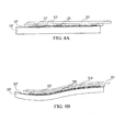
- FIGS. 4A and 4B show only one conductor 120, 320, respectively, it is to be understood that exemplary embodiments also may include at least one second conductor, such as conductors 121, 321, respectively described above in connection with FIGS. 1A and 3A . Further, electrical connection between the first contact 101, 301 and the underlying semiconducting surface, conductive or insulating surface of a semiconductor device, or a flexible circuit board can be made by conductors 121, 321 through the bonding and/or barrier layers.
- the above-discussed exemplary embodiments may also include multiple electrochemical devices stacked upon a semiconducting surface or the conductive or insulating (e.g., packaging) surface of a semiconductor device.
- the above-discussed exemplary embodiments may also include multiple electrochemical devices stacked upon the first electrical contact 301.
- the present exemplary embodiments provide alternative schemes to encapsulate the chemically and mechanically sensitive layers of electrochemical devices, which are less expensive than prior encapsulation schemes using gold foil.
- the above exemplary embodiments also avoid problems of other prior schemes relating to blow out of the seals of a metal and plastic pouch encapsulating an electrochemical device resulting from temperature changes, which cause the gas within the metal and plastic pouch to expand and/or contract.
- the exemplary embodiments described herein also provide a rechargeable secondary battery directly fabricated on a semiconductor device such as an integrated circuit. Such batteries provide power during times when the circuit is powered off and are quickly and easily recharged when power resumes. Critical circuitry may benefit from localized power provided by such batteries.
- the exemplary embodiments also provide for less expensive and more reliable encapsulating approaches, and better approaches to providing electrically conductive contacts, including encapsulation that is substantially thinner than known encapsulation methods.
- the exemplary embodiments also provide flexible integrated circuits and/or flexible printed circuit boards with thin film flexible batteries coupled thereon.
- a conductive material provided in an opening in the bonding layer, such as the slit
- electrical contact between the battery cell structure 115, 315 and first electrical contact 101, 301 may be provided by a number of other ways.
- embedding a conductive powder within an adhesive forming the bonding layer 110, 310 may provide electrical conduction between the cell structure 115, 315 and the first contact 101, 301.
- a conductive powder such as a metallic powder (e.g., nickel powder) can be embedded in an adhesive bonding layer 110, 310 at one or more selected areas within an adhesive bonding layer 110, 310 and between the contact 101, 301 and the battery cell structure 115, 315.
- the electrochemical device may comprise a discrete device (e.g., fully packaged with its own substrate and own encapsulation) on a semiconductor surface, a conducting or insulating surface of a semiconductor device or a flexible printed circuit board.
- a discrete device e.g., fully packaged with its own substrate and own encapsulation
- the electrochemical device may be fabricated as a discrete device, and then integrated as a whole together with its substrate and its encapsulation.
Landscapes
- Chemical & Material Sciences (AREA)
- Chemical Kinetics & Catalysis (AREA)
- Electrochemistry (AREA)
- General Chemical & Material Sciences (AREA)
- Engineering & Computer Science (AREA)
- Manufacturing & Machinery (AREA)
- Materials Engineering (AREA)
- Inorganic Chemistry (AREA)
- Physics & Mathematics (AREA)
- Condensed Matter Physics & Semiconductors (AREA)
- General Physics & Mathematics (AREA)
- Connection Of Batteries Or Terminals (AREA)
- Battery Mounting, Suspending (AREA)
- Secondary Cells (AREA)
- Sealing Battery Cases Or Jackets (AREA)
- Primary Cells (AREA)
- Battery Electrode And Active Subsutance (AREA)
- Laminated Bodies (AREA)
Description
- The field of this invention is the device, composition, method of depositing and fabrication of flexible solid-state, thin-film, secondary and primary electrochemical devices, including batteries, onto a semiconducting surface, onto a conductive or insulating surface of a semiconductor device, such as integrated circuit chips, or onto a circuit board, such as printed circuit board.
- Typical electrochemical devices comprise multiple electrically active layers such as an anode, cathode, electrolyte, substrate, current collectors, etc. Some layers, such as, for example, an anode layer comprising lithium, are comprised of materials that are very environmentally sensitive. The substrate may, for example, not be a separate battery element but instead be provided by a semiconducting surface or onto a conductive or insulating packaging surface of a semiconductor device to which the battery is attached. Such batteries require an encapsulation to protect such environmentally sensitive material. Some schemes encapsulate the sensitive layers of electrochemical devices, such as encapsulation with gold foil. Other schemes encapsulate the device with pouch, for example, made of metal and plastic, that seals around the perimeter of the device.
- Document
WO 2005/067645 A2 describes a layered barrier structure, wherein a system provides an environmental barrier for providing a circuit having a thin-film battery connected to an electronic circuit. The environmental barrier is deposited as alternating layers, at least one of the layers providing a smoothing, planarizing, and/or leveling physical-configuration function, and at least one other layer providing a diffusion-barrier function. The layer providing the physical-configuration function includes a photoresist, a photodefinable, an energy-definable and/or a maskable layer. The physical-configuration layer may also be a dielectric. A layered structure including a plurality of pairs of layers, wherein each pair includes a physical configuration layer and a barrier layer with low gas-transmission rates, is provided. - The invention is defined by the features of the independent claims. The dependent claims are directed to preferred embodiments of the invention.
- The first electrical contact may, for example, include an encapsulate metal. The bonding layer may be an adhesive material, an insulating material, a plastic, a polymeric material, glass, and/or fiberglass. An insulative reinforcement layer may be embedded within the bonding layer. Such a reinforcement layer may be selectively conductive. The conductor may be, for example, a tab, a wire, a metal strip, a metal ribbon, multiple wires, multiple metal strips, multiple metal ribbons, a wire mesh, perforated metal, a metal coating applied to the adhesive layer, or a disk. The conductor may be woven within the bonding layer and the bonding layer may include a slit within which the embedded conductor is woven.
- The battery cell structure may include an anode, an electrolyte, a cathode, and a barrier layer. The cathode may, for example, not be annealed at all, annealed at lower temperatures, or annealed at higher temperatures, by using convection furnaces, rapid thermal anneal methods, or by a laser annealing and/or crystallization process.
-
-
FIG. 1A shows a side view of an example of a thin film battery with a semiconducting surface or the conductive or insulating surface of a semiconductor device or a flexible printed circuit board according to an exemplary embodiment of the present invention. -
FIG. 1B shows a side view of another example of a thin film battery witch a semiconducting surface or the conductive or insulating packaging surface of a semiconductor device or a flexible printed circuit board according to an exemplary embodiment of the present invention. -
FIG. 2 shows a side view of an example of a thin film battery with a semiconducting surface or the conductive or insulating surface of a semiconductor device according to another exemplary embodiment of the present invention. -
FIG. 3A shows a side view of an exemplary thin film battery on a semiconducting surface or the conductive or insulating packaging surface of a semiconductor device or a flexible printed circuit board according to another exemplary embodiment of the present invention. -
FIG. 3B shows a side view of an exemplary thin film battery on a semiconducting surface or the conductive or insulating surface of a semiconductor device or flexible printed circuit board according to another exemplary embodiment of the present invention. -
FIG. 3C shows a top view of an exemplary thin film battery on a semiconducting surface or the conductive or insulating surface of a semiconductor device or flexible printed circuit board according to another exemplary embodiment of the present invention. -
FIG. 4A shows a side view of an exemplary thin film battery on a semiconducting surface or the conductive or insulating surface of a semiconductor device according to another exemplary embodiment of the present invention. -
FIG. 4B shows a side view of an exemplary thin film battery on a flexible printed circuit board according to another exemplary embodiment of the present invention. -
FIG. 1A shows a side view of an electrochemical device according to one exemplary embodiment of the present invention. In this embodiment, afirst contact 101 is coupled withbonding layer 110 with a portion of thefirst contact 101 extending past thebonding layer 110. Thebonding layer 110 may, for example, be bonded with thecell structure 115. A semiconducting surface or the conductive or insulating surface of asemiconductor device 105 is placed under thebattery cell structure 115. An insulating surface of thesemiconductor device 105 may be, for example, an insulating packaging surface of a semiconductor device or an upper insulating surface the semiconductor device. A conductive surface may include, for example, a conductive contact pad, a conductive line, conductive via or other conductive layer formed on or at the device surface. A conductive surface also may be formed together with an insulating surface, such as a conductive surface formed on a packaging surface of a semiconductor device. Shown embedded within thebonding layer 110 is a first embeddedconductor 120. This first embedded conductor120, for example, creates a selectively conductive bonding layer. A selectivelyconductive bonding layer 110 permits conduction from thecell structure 115 through thebonding layer 110 to thefirst contact 101 at specific points, and yet provides insulation between thefirst contact 101 and the semiconducting surface or the conductive or insulating surface of asemiconductor device 105. Other types of battery cell structures may be also be included. - The electrochemical device may have a second embedded
conductor 121 that selectively creates an electrical contact between thefirst contact 101 and the semiconducting surface or the conductive or insulating packaging surface of asemiconductor device 105. In this case, the semiconducting surface or the conductive or insulating surface of asemiconductor device 105 must be selectively insulating between the contacts points at which the first embeddedconductor 120 and the second embeddedconductor 121 meet the semiconducting surface or the conductive or insulating (e.g., packaging) surface of asemiconductor device 105. -
FIG. 1B shows a side view of an electrochemical device according to an exemplary embodiment of the present invention. In this embodiment, afirst contact 101 is coupled with thebattery cell structure 115. Abonding layer 110 is coupled to thebattery cell structure 115 and a portion of thefirst contact 101, which extends past thebonding layer 110. A semiconducting surface or the conductive or insulating surface of asemiconductor device 105 is coupled with thebonding layer 110. Shown embedded within thebonding layer 110 is the first embeddedconductor 120. This first embeddedconductor 120, for example, creates a selectively conductive bonding layer. A selectivelyconductive bonding layer 110 permits conduction from thecell structure 115 through thebonding layer 110 to the semiconducting surface or the conductive or insulating (e.g., packaging) surface of asemiconductor device 105 at specific points, and yet provides insulation between thefirst contact 101 and the semiconducting surface or the conductive or insulating surface of asemiconductor device 105. The electrochemical device may have a second embeddedconductor 121 that selectively creates an electrical contact between thefirst contact 101 and the semiconducting surface or the conductive or insulating surface of asemiconductor device 105. In this case the semiconducting surface or the conductive or insulating surface of asemiconductor device 105 must be selectively insulating between the contact points at which the first embeddedconductor 120 and the second embeddedconductor 121 meet the semiconducting surface or the conductive or insulating packaging surface of asemiconductor device 105. The first embeddedconductor 120 and the second embeddedconductor 121 may be placed within thebonding layer 110 in many different ways. For example, a metal tab, a metal wire, a metal strip, a metal ribbon, multiple metal wires, multiple metal strips, multiple metal ribbons, a metal wire mesh, perforated metal foil, perforated metal, a metal coating applied to the adhesive layer, a metallic disk, a metallically coated fiberglass or combinations thereof may be used. In each of these examples, the first embeddedconductor 120 and the second embeddedconductor 121 can provide electrical conduction between thecell structure 115 and thefirst contact 101 and theboding layer 110 provides insulation between thefirst contact 101 and the semiconducting surface or the conductive or insulating surface of asemiconductor device 105. In some embodiments, the embeddedconductors bonding layer 110. The embeddedconductors bonding layer 110. In some embodiments slits within thebonding layer 110 may be made in order to weave or place the embeddedconductors bonding layer 110. Also, for example, holes or other means may be used to place the embeddedconductors bonding layer 110. - In another exemplary embodiment of the present invention, a reinforcement layer may be placed within the bonding layer. For example, a fiberglass material may cover half of one surface of the bonding layer, woven through the layer and then cover the other half of the bonding layer. Such a layer of fiberglass without a conductive coating would insulate the materials placed between. The fiberglass may be coated in a localized area with a conductive material. Such conductive coatings can coat the fiberglass area in the top and bottom surface of the bonding layer. In such an embodiment, for example, the fiberglass may conduct between the upper contact and the cell. Conductive material may be disposed on the fiberglass using ink jet, silk screen, plasma deposition, e-beam deposition, spray and/or brush methods. Other materials may be used rather than fiberglass, such as, for example, Kevlar®, plastic, glass or other insulating materials.
- Another exemplary embodiment of the present invention may provide for selective contact between the first contact and the battery cell structure through holes in the bonding layer. In such an embodiment, holes in the bonding layer may allow the first contact and battery cell structure to remain in contact. The layers may be, for example, pressed together to create a contact. Alternatively, conductive glues or inks may be applied in or near the hole area in the bonding layer to make the contact between the layers. Lithium may also be used.
- The embedded
conductors - The
electrochemical device 115 may include a cathode, anode and electrolyte. For example, the cathode may comprise LiCoO2, the anode may comprise Lithium and the electrolyte may comprise LIPON. Other electrochemical devices may be used as needed. - The
electrochemical device 115 may be coupled with the semiconducting surface or the conductive or insulating packaging surface of asemiconductor device 105 in a number of ways. In one embodiment, the electrochemical device, for example, may be coupled with the semiconducting surface or the conducting or insulating surface of asemiconductor device 105 using glue. Glue, as used in this application, extends to any material that may adhere theelectrochemical device 115 to the semiconducting surface or the conducting or insulating surface of asemiconductor device 105. The glue may create either a mechanical or chemical bond between the two layers. Glue may also include chemically bonding the two layers without introducing another material or layer. Glue, for example, may include but is not limited to cement glue and resin glue. The glue may be electrically conducting, semi-conducting, or insulating. - In another exemplary embodiment, the semiconducting surface or the conductive or insulating (e.g., packaging) surface of a
semiconductor device 105 acts as a substrate for the battery. The semiconducting surface or the conductive or insulating packaging surface of asemiconductor device 105 is provided and theelectrochemical device 115 may be deposited thereon. Theelectrochemical device 115 may also be glued to the semiconducting surface or the conductive or insulating packaging surface of asemiconductor device 105. - In an exemplary embodiment, a LiCoO2 cathode layer is deposited on the semiconducting surface or the conducting or insulating surface of a
semiconductor device 105. A number of deposition techniques are known in the art, these include, but are not limited to reactive or non-reactive RF magnetron sputtering, reactive or non-reactive pulsed DC magnetron sputtering, reactive or non-reactive DC diode sputtering, reactive or non-reactive thermal (resistive) evaporation, reactive or non-reactive electron beam evaporation, ion-beam assisted deposition, plasma enhanced chemical vapor deposition, or deposition methods, which may include, for example, spin coating, ink-jetting, thermal spray deposition, dip coating or the like. As part of the fabrication process, for example, the cathode may be annealed using a thermal anneal such as anneal at lower temperatures, anneal at higher temperatures, or by using convection furnaces or rapid thermal anneal methods. Another or an alternative post-deposition anneal may include laser annealing to improve the crystallization of the LiCoO2 layer so as to fine-tune and optimize its chemical properties, such as its electrochemical potential, its energy, its power performance, and its reversible lattice parameters on electrochemical and thermal cycling. - Following deposition of the cathode layer, an electrolyte may be deposited on the cathode, followed by an anode. Again, these layers may be deposited by any of a number of processes common in the art. In one specific embodiment, once the
electrochemical device 115 has been deposited on the semiconducting surface or the conducting or insulating surface of asemiconductor device 105, abonding layer 110 may be placed between the electrochemical device and a firstelectrical contact 101. In this specific embodiment shown inFIG. 1A , ametal encapsulate layer 101 may also be the first contact. In another specific embodiment, once theelectrochemical device 115 has been deposited on the firstelectrical contact 101, abonding layer 110 may be placed between theelectrochemical device 115 and the semiconducting surface or the conducting or insulating surface of asemiconductor device 105. In this specific embodiment shown inFIG. 1B , ametal encapsulate layer 101 may also be the first contact. As described above, the first contact may be a metal foil, for example, may be made of stainless steel or any other metallic substance having the necessary characteristics and properties such as a requisite amount of conductivity. The metal foil may preferably comprise a solderable alloy, for instance, alloys of copper, nickel, or tin. The first contact may be, for example, less than 100 microns thick, less than 50 microns thick, or less than 25 microns thick. - The
bonding layer 110 may include, for example, an adhesive material, an insulating material, polymeric material, glass, Kevlar®, reinforcement materials, and fiberglass. The embeddedconductors -
FIG. 2 shows a second embodiment of a thin film battery on a chip. In this embodiment the battery may include a semiconducting surface or the conductive or insulating packaging surface of asemiconductor device 105, acathode layer 145 deposited on the semiconducting surface or the conductive or insulating packaging surface of asemiconductor device 105, anelectrolyte 150, ananode 165, amodulating layer 160, anencapsulate 155, an anodecurrent collector 170 and aninsulator 175. For example, thecathode 145 may comprise LiCoO2, theanode 160 may comprise Lithium and theelectrolyte 150 may comprise LIPON. Other electrochemical devices may be used as needed. The encapsulate 155 may comprise a ceramic-metal composite laminate of a multiple of alternating layers of Zirconium Nitride and Zirconium or Titanium Nitride and Titanium. - The electrochemical device which may include the
cathode 145,electrolyte 150 andanode 155, may be semiconducting surface or the conductive or insulating packaging surface of asemiconductor device 105 in a number of ways. In one embodiment, the electrochemical device, for example, may be coupled with the substantially conductive, semiconducting surface or the conductive packaging surface of asemiconductor device 105 using glue. Glue, as used in this application, extends to any material that may adhere parts of the electrochemical device to the semiconducting surface or the conductive or insulating packaging surface of asemiconductor device 105. The glue may create either a mechanical or chemical bond between the two layers. Glue may also include chemically bonding the two layers without introducing another material or layer. The glue may be electrically conductive in order to use the semiconducting surface or the conductive or insulating packaging surface of asemiconductor device 105 as current collector. Glue, for example, may include but is not limited to electrically conductive cement glue and resin glue. - The
cathode 145 may also be deposited directly on the semiconducting surface or the conductive or insulating packaging surface of asemiconductor device 105. In a specific embodiment, a LiCoO2 cathode layer is deposited on semiconducting surface or the conductive or insulating packaging surface of asemiconductor device 105. A number of deposition techniques are known in the art, these include, but are not limited to reactive or non-reactive RF magnetron sputtering, reactive or non-reactive pulsed DC magnetron sputtering, reactive or non-reactive DC diode sputtering, reactive or non-reactive thermal (resistive) evaporation, reactive or non-reactive electron beam evaporation, ion-beam assisted deposition, plasma enhanced chemical vapor deposition, deposition methods, which may include, for example, spin coating, ink-jetting, thermal spray deposition, dip coating or the like. As part of the fabrication process for example, a post-deposition laser anneal may be used to improve the crystallization of thecathode layer 145 in order to fine-tune and optimize its chemical properties, such as its electrochemical potential, its energy, its power performance, and its reversible lattice parameters on electrochemical and thermal cycling. Examples of methods used to deposit LiCoO2 are disclosed inU.S. patent application Ser. No. 11/557,383, filed on November 7, 2006 - The semiconducting surface or the conductive or insulating packaging surface of a semiconductor device in the above embodiments may be part of any integrated circuit and may include, memory devices, processors or other logic circuits.
- Another embodiment of the present invention includes a battery deposited on a flexible printed circuit board including, for example, a first electrical contact; a bonding layer coupled with the first electrical contact and having an embedded conductor; at least one battery cell structure; and a flexible printed circuit board. A bonding layer and the at least one battery cell structure may be sandwiched between the first contact layer and the flexible printed circuit board. The bonding layer may be selectively conductive through the embedded conductor. The battery cell structure may further be in selective electrical contact with the first electrical contact via the embedded conductor.
-
FIG. 3A shows a side view of an electrochemical device according to another embodiment of the present invention. In this embodiment, afirst contact 301 is coupled withbonding layer 310 with a portion of thefirst contact 301 extending past thebonding layer 310. Thebonding layer 310 may, for example, be bonded with thecell structure 315. A flexible printedcircuit board 305 is placed under thebattery cell structure 315. Shown embedded within thebonding layer 310 is a first embeddedconductor 320. This first embeddedconductor 320, for example, creates a selectively conductive bonding layer. A selectivelyconductive bonding layer 310 permits conduction from thecell structure 315 through thebonding layer 310 to thefirst contact 301 at specific points, and yet provides insulation between thefirst contact 301 and theflexible circuit board 305. Also shown embedded within thebonding layer 310 is the second embeddedconductor 321. This second conductor, for example, further creates a selectively conductive bonding layer. The further selectivelyconductive boding layer 310 permits conduction from the flexible printedcircuit board 305 through thebonding layer 310 to thefirst contact 301 at specific points, and yet provides insulation between thefirst contact 301 and the flexible printedcircuit board 305. Other types of battery cell structures may be also be included. -
FIG. 3B shows a side view of an electrochemical device according to one exemplary embodiment of the present invention. In this embodiment, afirst contact 301 is coupled with thebattery cell structure 315. Abonding layer 310 is coupled to thebattery cell structure 315 and a portion of thefirst contact 301, which extends past thebonding layer 310. A flexible printedcircuit board 305 is coupled with thebonding layer 310. Shown embedded within thebonding layer 310 is the first embeddedconductor 320. This first embeddedconductor 320, for example, creates a selectively conductive bonding layer. A selectivelyconductive bonding layer 310 permits conduction from thecell structure 315 through thebonding layer 310 to the flexible printedcircuit board 305 at specific points, and yet provides insulation between thefirst contact 301 and the flexible printedcircuit board 305. The electrochemical device may have a second embeddedconductor 321 that selectively creates an electrical contact between thefirst contact 301 and the flexible printedcircuit board 305. In this case, the flexible printedcircuit board 305 must be selectively insulating between the contacts points at which the first embeddedconductor 320 and the second embeddedconductor 321 meet the flexible printedcircuit board 305. -
FIG. 3C is a top view of an exemplary electrochemical device integrated with aflexible circuit board 305, such as the exemplary devices described above with respect toFIGS. 3A and 3B . As shown inFIG. 3C ,conductive traces circuit board 305. Other types of conductive surfaces, such as contact pads, wiring, exposed conductive vias etc., or combinations thereof may be provided on the circuit board surface to receive the electrochemical device. In the plan view, the first embeddedconductor 320 is shown passing throughbonding layer 310 to make electrical contact withconductive trace 330, and the second embeddedconductor 321 is shown passing throughbonding layer 310 to make electrical contact withconductive trace 331. It should be appreciated that an analogous arrangement can be achieved with respect to the examples including a semiconducting surface or the conductive or insulating packaging surface of a semiconductor device, as described above with respect toFIGS. 1A and 1B . - The
flexible circuit board 305 may comprise, for example, multiple circuit board layers with and without traces, single or double sided, semi-rigid, a film, and/or a polyimide film. - The embedded
conductors bonding layer 310 in many different ways. For example, a metal tab, a metal wire, a metal strip, a metal ribbon, multiple metal wires, multiple metal strips, multiple metal ribbons, a metal wire mesh, perforated metal foil, perforated metal, a metal coating applied to the adhesive layer, a metallic disk, a metallically coated fiberglass or combinations thereof may be used. In each of these examples, the first embeddedconductor 320 can provide selective electrical conduction between thecell structure 315 and thefirst contact 301 or the flexible printedcircuit board 305, and yet provide insulation between thebattery cell structure 315 and thefirst contact 301 or the flexible printedcircuit board 305. Also in each of these examples, the second embeddedconductor 321 can provide selective electrical conduction between thefirst contact 301 and the flexible printedcircuit board 305 and yet provide insulation between thefirst contact 301 and the flexible printedcircuit board 305. In some embodiments the first embeddedconductor 320 may be woven within thebonding layer 310. The first embeddedconductor 320 may be, for example, disks embedded within thebonding layer 310. In some embodiments slits within thebonding layer 310 may be made in order to weave or place the first embeddedconductor 320 through thebonding layer 310. Also, for example, holes or other means may be used to place the first embeddedconductor 320 through thebonding layer 310. In some embodiments the second embeddedconductor 321 may be woven within thebonding layer 310. The second embeddedconductor 321 may be, for example, disks embedded within thebonding layer 310. In some embodiments slits within thebonding layer 310 may be made in order to weave or place the second embeddedconductor 321 through thebonding layer 310. Also, for example, holes or other means may be used to place the second embeddedconductor 321 through thebonding layer 310. - The
electrochemical device 315 may include a cathode, anode and electrolyte. For example, the cathode may comprise LiCoO2, the anode may comprise Lithium and the electrolyte may comprise LIPON. Other electrochemical devices may be used as needed. - The
electrochemical device 315 may be coupled with the flexible printedcircuit board 305 in a number of ways. In one embodiment, theelectrochemical device 315, for example, may be coupled with the flexible printedcircuit board 305 using glue. Glue, as used in this application, extends to any material that may adhere theelectrochemical device 315 to the flexible printedcircuit board 305. The glue may create either a mechanical or chemical bond between the two layers. Glue may also include chemically bonding the two layers without introducing another material or layer. Glue, for example, may include but is not limited to cement glue and resin glue. The glue may be electrically conducting, semi-conducting, or insulating. - The
electrochemical device 315 may be coupled with the firstelectrical contact 301 in a number of ways. In one embodiment, theelectrochemical device 315, for example, may be coupled with the firstelectrical contact 301 using glue. Glue, as used in this application, extends to any material that may adhere theelectrochemical device 315 to the firstelectrical contact 301. The glue may create either a mechanical or chemical bond between the two layers. Glue may also include chemically bonding the two layers without introducing another material or layer. Glue, for example, may include but is not limited to cement glue and resin glue. The glue may be electrically conducting, semi-conducting, or insulating. - In another embodiment the flexible printed
circuit board 305 acts as a substrate for the battery, which may be deposited thereon. - In another embodiment the first
electrical contact 301 acts as a substrate for the battery, which may be deposited thereon. - In another embodiment the flexible printed
circuit board 305 acts as an encapsulate for the battery. - In another embodiment the first
electrical contact 301 acts as an encapsulate for the battery. - In another exemplary embodiment shown in
FIG. 4A , a thin film battery is provided on a semiconducting surface or the conductive or insulating surface of a semiconductor device with a barrier layer therebetween. Elements depicted inFigure 4A like those above inFIG. 1A are shown having the same reference numbers. In this embodiment, afirst contact 101 is coupled withbonding layer 110 with a portion of thefirst contact 101 extending past thebonding layer 110. Thebonding layer 110 may, for example, be bonded with thecell structure 115. A semiconducting surface or the conductive or insulating (e.g., packaging) surface of asemiconductor device 105 with abarrier layer 107 is placed under thebattery cell structure 115. - In this embodiment,
barrier layer 107 may include, for example, titanium nitride. Thebarrier layer 107 may also comprise a semiconducting surface or the conductive or insulating packaging surface of asemiconductor device 105. A conductive surface may include, for example, a conductive contact pad, a conductive line, conductive via or other conductive layer formed on or at the device surface. A conductive surface also may be formed together with an insulating surface, such as a conductive surface formed on a packaging surface of a semiconductor device. An insulating surface of thesemiconductor device 105 may be, for example, an insulating packaging surface of a semiconductor device or an upper insulating surface the semiconductor device. Shown embedded within thebonding layer 110 isconductor 120. Thisconductor 120, for example, creates a selectively conductive bonding layer. A selectivelyconductive bonding layer 110 permits conduction from thecell structure 115 through thebonding layer 110 to thefirst contact 101 at specific points, and yet provides insulation between thefirst contact 101 and thebarrier layer 107. Other types of battery cell structures may be also be included. - The
electrochemical device 115 may be coupled with the semiconducting surface or the conductive or insulating (e.g., packaging) surface of asemiconductor device 105 andbarrier layer 107 in a number of ways. In one embodiment, the electrochemical device, for example, may be coupled with the barrier layer using glue. Glue, as used in this application, extends to any material that may adhere theelectrochemical device 115 to thebarrier layer 107. The glue may create either a mechanical or chemical bond between the two layers. Glue may also include chemically bonding the two layers without introducing another material or layer. Glue, for example, may include but is not limited to cement glue and resin glue. The glue may be electrically conducting, semi-conducting, or insulating. - In another exemplary embodiment the semiconducting surface or the conductive or insulating packaging surface of a
semiconductor device 105 acts as a substrate for the battery. The semiconducting surface or the conductive or insulating packaging surface of asemiconductor device 105 is provided and thebarrier layer 107 may be deposited thereon. Thebarrier layer 107 may also be glued to the semiconducting surface or the conductive or insulating packaging surface of asemiconductor device 105. Once thebarrier layer 107 and thesubstrate 105 have been prepared, theelectrochemical device 115 may be deposited directly on thebarrier layer 107. - In an exemplary embodiment, a LiCoO2 cathode layer is deposited on the
barrier layer 107 by way of methods described above. - In yet another exemplary embodiment shown in
FIG. 4B , a thin film battery is provided on a flexible circuit board. Elements depicted inFigure 4B like those above inFIG. 3A are shown having the same reference numbers. In this embodiment, afirst contact 301 is coupled withbonding layer 310 with a portion of thefirst contact 301 extending past thebonding layer 310. Thebonding layer 310 may, for example, be bonded with thecell structure 315. A flexible printedcircuit board 305, such as described above, and abarrier layer 307 is placed under thebattery cell structure 315. In this embodiment, thebarrier layer 307 may, for example, include titanium nitride. Shown embedded within thebonding layer 310 isconductor 320. Thisconductor 320, for example, creates a selectively conductive bonding layer. A selectivelyconductive bonding layer 310 permits conduction from thecell structure 315 through thebonding layer 310 to thefirst contact 301 at specific points, and yet provides insulation between thefirst contact 301 and thebarrier layer 307. Theconductor 320 may be provided within thebonding layer 310 as described above. In each of these examples, theconductor 320 can provide electrical conduction between thecell structure 315 and thefirst contact 301 and yet provide insulation between thefirst contact 301 and thebarrier layer 307. - The
electrochemical device 315 may be coupled with the semiconducting surface or the conductive or insulating packaging surface of asemiconductor device 305 andbarrier layer 307 in a number of ways. In one embodiment, the electrochemical device, for example, may be coupled with the barrier layer using glue. Glue, as used in this application, extends to any material that may adhere theelectrochemical device 315 to thebarrier layer 307. The glue may create either a mechanical or chemical bond between the two layers. Glue may also include chemically bonding the two layers without introducing another material or layer. Glue, for example, may include but is not limited to cement glue and resin glue. The glue may be electrically conducting, semi-conducting, or insulating. - In another embodiment the flexible printed
circuit board 305 acts as a substrate for the battery and thebarrier layer 307 may be deposited thereon. Thebarrier layer 307 may also be glued to the flexible printedcircuit board 305. Once thebarrier layer 307 and the printedcircuit board 305 have been prepared, theelectrochemical device 315 may be deposited directly on thebarrier layer 307. - While
FIGS. 4A and 4B show only oneconductor conductors FIGS. 1A and3A . Further, electrical connection between thefirst contact conductors - The above-discussed exemplary embodiments may also include multiple electrochemical devices stacked upon a semiconducting surface or the conductive or insulating (e.g., packaging) surface of a semiconductor device.
- The above-discussed exemplary embodiments may also include multiple electrochemical devices stacked upon the first
electrical contact 301. - The present exemplary embodiments provide alternative schemes to encapsulate the chemically and mechanically sensitive layers of electrochemical devices, which are less expensive than prior encapsulation schemes using gold foil. The above exemplary embodiments also avoid problems of other prior schemes relating to blow out of the seals of a metal and plastic pouch encapsulating an electrochemical device resulting from temperature changes, which cause the gas within the metal and plastic pouch to expand and/or contract.
- The exemplary embodiments described herein also provide a rechargeable secondary battery directly fabricated on a semiconductor device such as an integrated circuit. Such batteries provide power during times when the circuit is powered off and are quickly and easily recharged when power resumes. Critical circuitry may benefit from localized power provided by such batteries. The exemplary embodiments also provide for less expensive and more reliable encapsulating approaches, and better approaches to providing electrically conductive contacts, including encapsulation that is substantially thinner than known encapsulation methods. The exemplary embodiments also provide flexible integrated circuits and/or flexible printed circuit boards with thin film flexible batteries coupled thereon.
- Although the above examples describe a conductive material provided in an opening in the bonding layer, such as the slit, it should be appreciated that electrical contact between the
battery cell structure electrical contact bonding layer cell structure first contact adhesive bonding layer adhesive bonding layer contact battery cell structure battery cell structure first contact - The same holds true for the electrical contact between the
battery cell structure semiconductor device 105 or the flexible printedcircuit board 305. The same also holds true for the electrical contact between thefirst contact semiconductor device 105 or the flexible printedcircuit board 305. - Additionally, it should be appreciated that the electrochemical device may comprise a discrete device (e.g., fully packaged with its own substrate and own encapsulation) on a semiconductor surface, a conducting or insulating surface of a semiconductor device or a flexible printed circuit board. For example, prior to its integration onto the semiconducting surface or a conductive or insulating surface of a semiconductor device or into or onto a flexible printed circuit board, the electrochemical device may be fabricated as a discrete device, and then integrated as a whole together with its substrate and its encapsulation.
Claims (26)
- A battery on an integrated circuit or on a flexible printed circuit board, comprising:a first electrical contact (101; 301);a bonding layer (110; 310) coupled with said first electrical contact (101; 301) and comprising a first embedded conductor (120; 320);at least one battery cell structure (115; 315) in selective electrical contact with said first electrical contact (101; 301) via said first embedded conductor (120; 320); anda semiconducting surface or a conductive or insulating packaging surface of a semiconductor device (105) or a flexible printed circuit board (305);wherein said bonding layer (110; 310) and said at least one battery cell structure (115; 315) are sandwiched between said first electrical contact (101; 301) and said semiconducting surface or the conductive or insulating surface of a semiconductor device (105) or said flexible printed circuit board (305); andwherein said battery further comprises said first electrical contact (101; 301) in selective electrical contact with the semiconducting surface or the conductive or insulating packaging surface of a semiconductor device (105) or the flexible printed circuit board (305) via a second embedded conductor (121; 321) embedded in the boding layer (110; 310).
- The battery of claim 1, wherein said first electrical contact (101; 301) further comprises an encapsulate metal.
- The battery of claim 1, wherein said semiconducting surface or the conductive or insulating packaging surface of a semiconductor device (105) acts as an encapsulate of said at least one battery cell structure (115; 315).
- The battery of claim 1, wherein said bonding layer (110; 310) comprises a material selected from the group comprising an adhesive material, an insulating material, plastic, glass, reinforcement materials, and fiberglass.
- The battery of claim 1, wherein said embedded conductor is selected from the group consisting of a tab, a wire, metal strip, a metal ribbon multiple wires, multiple metal strips, multiple metal ribbons, a wire mesh, perforated metal, a metal coating applied to the adhesive layer, and a disk.
- The battery of claim 1, wherein said embedded conductor is woven within said bonding layer (110; 310).
- The battery of claim 6, wherein said bonding layer (110; 310) comprises a slit within which said embedded conductor is woven.
- The battery of claim 1, wherein said first contact comprises a material selected from the group consisting of gold, platinum, stainless steel, titanium, vanadium, chromium, manganese, iron, cobalt, nickel, copper, zirconium, aluminum, indium, nickel, copper, silver, carbon, bronze, brass, beryllium, and oxides, nitrides, carbides and alloys thereof.
- The battery of claim 1, wherein said battery cell structure (115; 315) comprises at least:an anode (165),an electrolyte (150); anda cathode (145).
- The battery of claim 9, wherein said cathode (145) is annealed.
- The battery of claim 9, wherein said cathode (145) is crystallized.
- The battery of claim 1, wherein the first contact acts as a positive terminal of said battery cell structure (115; 315).
- The battery of claim 1, wherein the first contact acts as a negative terminal of said battery cell structure (115; 315).
- The battery of claim 1, further comprising a barrier layer (107) between said battery cell structure (115; 315) and said semiconducting surface or the conductive or insulating surface of a semiconductor device (105) or the flexible printed circuit board (305).
- The battery of claim 1, wherein said first contact comprises a metal foil.
- The battery of claim 1, further comprising a plurality of battery cell structures (115; 315) stacked one upon another with at least one metal foil encapsulating each battery cell structure (115; 315).
- The battery of claim 1, wherein portions of said first contact are coated with an insulating material.
- The battery of claim 1, said battery cell structure (115; 315) further comprising a substrate sandwiched between said battery cell structure (115; 315) and said first electrical contact (101; 301).
- The battery of claim 1, further comprising an encapsulate sandwiched between said bonding layer (110; 310) and said first electrical contact (101; 301).
- The battery of claim 1, wherein said flexible printed circuit board (305) is selected from the group consisting of multiple circuit board layers with and without traces, single sided printed circuit board, double sided printed circuit board, and a semi-rigid printed circuit board.
- The battery of claim 1, wherein said flexible printed circuit board (305) comprises a polyimide film.
- A method of manufacturing a battery on a semiconducting surface or a conductive or insulating surface of a semiconductor device (105) or on a flexible printed circuit board (305), comprising:creating a selectively conductive bonding layer (110; 310) comprising a first embedded conductor (120; 320);coupling said bonding layer (110; 310) with a first contact layer (101; 301);coupling a first side of a battery cell structure (115; 315) with a semiconducting surface or a conductive or insulating surface of a semiconductor device (105) or a flexible printed circuit board (305); andcoupling a second side of said battery cell structure (115; 315) with said bonding layer (110; 310);electrically contacting said second side of said battery cell structure (115; 315) with said first contact layer (101; 301) via said first embedded conductor (120; 320); andcoupling the first contact layer (101; 301) with the semiconducting surface or conductive or insulating surface of a semiconductor device (105) or the flexible printed circuit board (305) via a second embedded conductor (121; 321) embedded in the bonding layer (110; 310).
- The method of claim 22, wherein said step of coupling a first side of a battery cell structure (115; 315) with a semiconducting surface or a conductive or insulating surface of a semiconductor device (105) or with a flexible printed circuit board (305) comprises gluing a first side of a battery cell structure (115; 315) with a semiconducting surface or the conductive or insulating surface of a semiconductor device (105) or with the flexible printed circuit board (305).
- The method of claim 22, further comprising depositing a cathode (145) on said semiconducting surface or the conductive or insulating packaging surface of a semiconductor device (105) or on said flexible printed circuit board (305).
- The method of claim 24, further comprising crystallizing said cathode (145) with a laser.
- The method of claim 24, further comprising annealing said cathode (145) via rapid thermal anneal.
Priority Applications (1)
| Application Number | Priority Date | Filing Date | Title |
|---|---|---|---|
| EP14164006.0A EP2755267B1 (en) | 2006-05-12 | 2007-05-14 | Thin film battery on an integrated circuit or circuit board and method thereof |
Applications Claiming Priority (2)
| Application Number | Priority Date | Filing Date | Title |
|---|---|---|---|
| US79990406P | 2006-05-12 | 2006-05-12 | |
| PCT/US2007/068915 WO2007134308A2 (en) | 2006-05-12 | 2007-05-14 | Thin film battery on an integrated circuit or circuit board and method thereof |
Related Child Applications (2)
| Application Number | Title | Priority Date | Filing Date |
|---|---|---|---|
| EP14164006.0A Division-Into EP2755267B1 (en) | 2006-05-12 | 2007-05-14 | Thin film battery on an integrated circuit or circuit board and method thereof |
| EP14164006.0A Division EP2755267B1 (en) | 2006-05-12 | 2007-05-14 | Thin film battery on an integrated circuit or circuit board and method thereof |
Publications (3)
| Publication Number | Publication Date |
|---|---|
| EP2033247A2 EP2033247A2 (en) | 2009-03-11 |
| EP2033247A4 EP2033247A4 (en) | 2011-06-29 |
| EP2033247B1 true EP2033247B1 (en) | 2014-08-06 |
Family
ID=38694776
Family Applications (2)
| Application Number | Title | Priority Date | Filing Date |
|---|---|---|---|
| EP14164006.0A Active EP2755267B1 (en) | 2006-05-12 | 2007-05-14 | Thin film battery on an integrated circuit or circuit board and method thereof |
| EP07797463.2A Active EP2033247B1 (en) | 2006-05-12 | 2007-05-14 | Thin film battery on an integrated circuit or circuit board and method thereof |
Family Applications Before (1)
| Application Number | Title | Priority Date | Filing Date |
|---|---|---|---|
| EP14164006.0A Active EP2755267B1 (en) | 2006-05-12 | 2007-05-14 | Thin film battery on an integrated circuit or circuit board and method thereof |
Country Status (6)
| Country | Link |
|---|---|
| EP (2) | EP2755267B1 (en) |
| JP (2) | JP5511374B2 (en) |
| KR (2) | KR101610572B1 (en) |
| CN (1) | CN101443937B (en) |
| TW (1) | TWI419397B (en) |
| WO (1) | WO2007134308A2 (en) |
Families Citing this family (14)
| Publication number | Priority date | Publication date | Assignee | Title |
|---|---|---|---|---|
| US8394522B2 (en) * | 2002-08-09 | 2013-03-12 | Infinite Power Solutions, Inc. | Robust metal film encapsulation |
| GB0823260D0 (en) | 2008-12-20 | 2009-01-28 | Qinetiq Ltd | Multi-functional composite |
| NZ598311A (en) * | 2009-08-14 | 2013-11-29 | Univ Michigan | DIRECT THERMAL SPRAY SYNTHESIS OF Li ION BATTERY COMPONENTS |
| KR101792287B1 (en) * | 2009-09-01 | 2017-10-31 | 사푸라스트 리써치 엘엘씨 | Printed circuit board with integrated thin film battery |
| DE102010040704A1 (en) * | 2010-09-14 | 2012-03-15 | Robert Bosch Gmbh | Method of constructing an electrical circuit and electrical circuit |
| JP5752412B2 (en) * | 2010-12-27 | 2015-07-22 | 株式会社アルバック | Thin-film lithium secondary battery manufacturing method and thin-film lithium secondary battery |
| US9614256B2 (en) * | 2014-03-31 | 2017-04-04 | Infineon Technologies Ag | Lithium ion battery, integrated circuit and method of manufacturing a lithium ion battery |
| WO2016092889A1 (en) * | 2014-12-09 | 2016-06-16 | 日本碍子株式会社 | Battery-equipped device |
| CN106161679B (en) * | 2015-03-30 | 2022-03-01 | 安徽精卓光显技术有限责任公司 | Portable terminal back cover battery and preparation method of portable terminal back cover battery |
| JP7023222B2 (en) * | 2015-10-02 | 2022-02-21 | アプライド マテリアルズ インコーポレイテッド | Methods and equipment for manufacturing flexible layer stacks, as well as flexible layer stacks. |
| CN106887562B (en) * | 2015-12-15 | 2020-12-04 | 小米科技有限责任公司 | Protection mainboard of battery cell, electronic terminal and assembly method of battery cell for electronic terminal |
| CN107732070B (en) * | 2017-10-13 | 2024-07-02 | 华霆(合肥)动力技术有限公司 | Battery module and assembling method |
| CN112332042B (en) * | 2020-11-10 | 2022-11-11 | 深圳新源柔性科技有限公司 | Electronic device and method for manufacturing the same |
| CN114184176A (en) * | 2021-11-15 | 2022-03-15 | 中建八局西南建设工程有限公司 | Micro-power-consumption flexible water flow tracking beacon based on Beidou positioning communication |
Family Cites Families (17)
| Publication number | Priority date | Publication date | Assignee | Title |
|---|---|---|---|---|
| US712316A (en) * | 1899-10-26 | 1902-10-28 | Francois Loppe | Electric accumulator. |
| US4518661A (en) * | 1982-09-28 | 1985-05-21 | Rippere Ralph E | Consolidation of wires by chemical deposition and products resulting therefrom |
| JPH01124248A (en) * | 1987-11-09 | 1989-05-17 | Matsushita Electric Ind Co Ltd | Electronic component |
| JPH09259932A (en) * | 1996-03-26 | 1997-10-03 | Toshiba Battery Co Ltd | Secondary battery with charging circuit |
| JP4085459B2 (en) * | 1998-03-02 | 2008-05-14 | セイコーエプソン株式会社 | Manufacturing method of three-dimensional device |
| DE60135100D1 (en) * | 2000-03-24 | 2008-09-11 | Cymbet Corp | E WITH ULTRA-THIN ELECTROLYTES |
| JP4129667B2 (en) * | 2000-04-21 | 2008-08-06 | 富士フイルム株式会社 | Battery built-in board |
| JP4132647B2 (en) * | 2000-11-21 | 2008-08-13 | シャープ株式会社 | Thin secondary battery |
| JP2002291176A (en) * | 2001-03-23 | 2002-10-04 | Nippon System Products Kk | Secondary battery mounting integrated circuit |
| US6517968B2 (en) * | 2001-06-11 | 2003-02-11 | Excellatron Solid State, Llc | Thin lithium film battery |
| FR2831331B1 (en) * | 2001-10-22 | 2004-11-19 | Commissariat Energie Atomique | METHOD FOR MANUFACTURING A MICRO-BATTERY |
| JP3960033B2 (en) * | 2001-12-19 | 2007-08-15 | 松下電器産業株式会社 | Stacked electrochemical device |
| US6885028B2 (en) * | 2002-03-25 | 2005-04-26 | Sharp Kabushiki Kaisha | Transistor array and active-matrix substrate |
| WO2004093223A2 (en) * | 2003-04-14 | 2004-10-28 | Massachusetts Institute Of Technology | Integrated thin film batteries on silicon integrated circuits |
| US7045246B2 (en) * | 2003-04-22 | 2006-05-16 | The Aerospace Corporation | Integrated thin film battery and circuit module |
| JP2007518246A (en) * | 2004-01-06 | 2007-07-05 | シンベット コーポーレーション | Layered barrier structure comprising one or more layers having a boundary and method of manufacturing the barrier structure |
| JP4150690B2 (en) * | 2004-03-29 | 2008-09-17 | 株式会社東芝 | Battery integrated semiconductor element |
-
2007
- 2007-05-11 TW TW096116929A patent/TWI419397B/en active
- 2007-05-14 EP EP14164006.0A patent/EP2755267B1/en active Active
- 2007-05-14 WO PCT/US2007/068915 patent/WO2007134308A2/en not_active Ceased
- 2007-05-14 JP JP2009510200A patent/JP5511374B2/en active Active
- 2007-05-14 KR KR1020147029445A patent/KR101610572B1/en active Active
- 2007-05-14 EP EP07797463.2A patent/EP2033247B1/en active Active
- 2007-05-14 CN CN200780016760XA patent/CN101443937B/en active Active
- 2007-05-14 KR KR1020087028511A patent/KR20090025213A/en not_active Abandoned
-
2014
- 2014-02-10 JP JP2014023698A patent/JP5876088B2/en active Active
Also Published As
| Publication number | Publication date |
|---|---|
| CN101443937B (en) | 2012-11-28 |
| JP2014132580A (en) | 2014-07-17 |
| KR101610572B1 (en) | 2016-04-07 |
| JP5511374B2 (en) | 2014-06-04 |
| TWI419397B (en) | 2013-12-11 |
| EP2755267A1 (en) | 2014-07-16 |
| KR20090025213A (en) | 2009-03-10 |
| WO2007134308A2 (en) | 2007-11-22 |
| JP2009537068A (en) | 2009-10-22 |
| TW200816546A (en) | 2008-04-01 |
| JP5876088B2 (en) | 2016-03-02 |
| CN101443937A (en) | 2009-05-27 |
| EP2033247A2 (en) | 2009-03-11 |
| EP2033247A4 (en) | 2011-06-29 |
| EP2755267B1 (en) | 2017-08-02 |
| KR20140135842A (en) | 2014-11-26 |
| WO2007134308A3 (en) | 2008-03-06 |
Similar Documents
| Publication | Publication Date | Title |
|---|---|---|
| US9634296B2 (en) | Thin film battery on an integrated circuit or circuit board and method thereof | |
| EP2755267B1 (en) | Thin film battery on an integrated circuit or circuit board and method thereof | |
| US10080291B2 (en) | Printed circuit board with integrated thin film battery | |
| US8236443B2 (en) | Metal film encapsulation | |
| US8394522B2 (en) | Robust metal film encapsulation | |
| US20190165342A1 (en) | Thin-film battery with adhesive layer | |
| US20090302804A1 (en) | Battery pack | |
| US8404376B2 (en) | Metal film encapsulation | |
| EP1997176B1 (en) | Metal film encapsulation | |
| US12362437B2 (en) | Multilayered flexible interconnect circuits for battery assemblies and methods of fabricating and installing thereof | |
| JP2007026982A (en) | Solid battery and battery-mounted integrated circuit device having the same |
Legal Events
| Date | Code | Title | Description |
|---|---|---|---|
| PUAI | Public reference made under article 153(3) epc to a published international application that has entered the european phase |
Free format text: ORIGINAL CODE: 0009012 |
|
| 17P | Request for examination filed |
Effective date: 20081211 |
|
| AK | Designated contracting states |
Kind code of ref document: A2 Designated state(s): AT BE BG CH CY CZ DE DK EE ES FI FR GB GR HU IE IS IT LI LT LU LV MC MT NL PL PT RO SE SI SK TR |
|
| AX | Request for extension of the european patent |
Extension state: AL BA HR MK RS |
|
| DAX | Request for extension of the european patent (deleted) | ||
| A4 | Supplementary search report drawn up and despatched |
Effective date: 20110530 |
|
| 17Q | First examination report despatched |
Effective date: 20120314 |
|
| REG | Reference to a national code |
Ref country code: DE Ref legal event code: R079 Ref document number: 602007038005 Country of ref document: DE Free format text: PREVIOUS MAIN CLASS: H01M0006140000 Ipc: H01M0002020000 |
|
| GRAP | Despatch of communication of intention to grant a patent |
Free format text: ORIGINAL CODE: EPIDOSNIGR1 |
|
| RIC1 | Information provided on ipc code assigned before grant |
Ipc: H01M 4/02 20060101ALN20140113BHEP Ipc: H01M 2/02 20060101AFI20140113BHEP Ipc: H01M 2/10 20060101ALI20140113BHEP Ipc: H01M 2/30 20060101ALI20140113BHEP Ipc: H01M 4/40 20060101ALN20140113BHEP Ipc: H01M 10/0562 20100101ALI20140113BHEP Ipc: H01M 10/052 20100101ALI20140113BHEP Ipc: H01M 2/26 20060101ALI20140113BHEP Ipc: H01L 23/58 20060101ALI20140113BHEP Ipc: H01M 4/04 20060101ALI20140113BHEP Ipc: H01M 10/04 20060101ALN20140113BHEP Ipc: H01M 4/1391 20100101ALI20140113BHEP Ipc: H01M 4/525 20100101ALN20140113BHEP Ipc: H01M 6/40 20060101ALI20140113BHEP |
|
| RIC1 | Information provided on ipc code assigned before grant |
Ipc: H01M 10/0562 20100101ALI20140131BHEP Ipc: H01M 10/052 20100101ALI20140131BHEP Ipc: H01M 4/40 20060101ALN20140131BHEP Ipc: H01M 6/40 20060101ALI20140131BHEP Ipc: H01M 2/30 20060101ALI20140131BHEP Ipc: H01M 2/10 20060101ALI20140131BHEP Ipc: H01L 23/58 20060101ALI20140131BHEP Ipc: H01M 4/525 20100101ALN20140131BHEP Ipc: H01M 2/26 20060101ALI20140131BHEP Ipc: H01M 10/04 20060101ALN20140131BHEP Ipc: H01M 2/02 20060101AFI20140131BHEP Ipc: H01M 4/04 20060101ALI20140131BHEP Ipc: H01M 4/1391 20100101ALI20140131BHEP Ipc: H01M 4/02 20060101ALN20140131BHEP |
|
| INTG | Intention to grant announced |
Effective date: 20140217 |
|
| GRAS | Grant fee paid |
Free format text: ORIGINAL CODE: EPIDOSNIGR3 |
|
| GRAA | (expected) grant |
Free format text: ORIGINAL CODE: 0009210 |
|
| AK | Designated contracting states |
Kind code of ref document: B1 Designated state(s): AT BE BG CH CY CZ DE DK EE ES FI FR GB GR HU IE IS IT LI LT LU LV MC MT NL PL PT RO SE SI SK TR |
|
| REG | Reference to a national code |
Ref country code: GB Ref legal event code: FG4D |
|
| REG | Reference to a national code |
Ref country code: AT Ref legal event code: REF Ref document number: 681382 Country of ref document: AT Kind code of ref document: T Effective date: 20140815 Ref country code: CH Ref legal event code: EP |
|
| REG | Reference to a national code |
Ref country code: IE Ref legal event code: FG4D |
|
| REG | Reference to a national code |
Ref country code: DE Ref legal event code: R096 Ref document number: 602007038005 Country of ref document: DE Effective date: 20140918 |
|
| REG | Reference to a national code |
Ref country code: AT Ref legal event code: MK05 Ref document number: 681382 Country of ref document: AT Kind code of ref document: T Effective date: 20140806 |
|
| REG | Reference to a national code |
Ref country code: NL Ref legal event code: VDEP Effective date: 20140806 |
|
| REG | Reference to a national code |
Ref country code: LT Ref legal event code: MG4D |
|
| PG25 | Lapsed in a contracting state [announced via postgrant information from national office to epo] |
Ref country code: PT Free format text: LAPSE BECAUSE OF FAILURE TO SUBMIT A TRANSLATION OF THE DESCRIPTION OR TO PAY THE FEE WITHIN THE PRESCRIBED TIME-LIMIT Effective date: 20141209 Ref country code: LT Free format text: LAPSE BECAUSE OF FAILURE TO SUBMIT A TRANSLATION OF THE DESCRIPTION OR TO PAY THE FEE WITHIN THE PRESCRIBED TIME-LIMIT Effective date: 20140806 Ref country code: SE Free format text: LAPSE BECAUSE OF FAILURE TO SUBMIT A TRANSLATION OF THE DESCRIPTION OR TO PAY THE FEE WITHIN THE PRESCRIBED TIME-LIMIT Effective date: 20140806 Ref country code: BG Free format text: LAPSE BECAUSE OF FAILURE TO SUBMIT A TRANSLATION OF THE DESCRIPTION OR TO PAY THE FEE WITHIN THE PRESCRIBED TIME-LIMIT Effective date: 20141106 Ref country code: FI Free format text: LAPSE BECAUSE OF FAILURE TO SUBMIT A TRANSLATION OF THE DESCRIPTION OR TO PAY THE FEE WITHIN THE PRESCRIBED TIME-LIMIT Effective date: 20140806 Ref country code: GR Free format text: LAPSE BECAUSE OF FAILURE TO SUBMIT A TRANSLATION OF THE DESCRIPTION OR TO PAY THE FEE WITHIN THE PRESCRIBED TIME-LIMIT Effective date: 20141107 Ref country code: ES Free format text: LAPSE BECAUSE OF FAILURE TO SUBMIT A TRANSLATION OF THE DESCRIPTION OR TO PAY THE FEE WITHIN THE PRESCRIBED TIME-LIMIT Effective date: 20140806 |
|
| PG25 | Lapsed in a contracting state [announced via postgrant information from national office to epo] |
Ref country code: NL Free format text: LAPSE BECAUSE OF FAILURE TO SUBMIT A TRANSLATION OF THE DESCRIPTION OR TO PAY THE FEE WITHIN THE PRESCRIBED TIME-LIMIT Effective date: 20140806 Ref country code: IS Free format text: LAPSE BECAUSE OF FAILURE TO SUBMIT A TRANSLATION OF THE DESCRIPTION OR TO PAY THE FEE WITHIN THE PRESCRIBED TIME-LIMIT Effective date: 20141206 Ref country code: AT Free format text: LAPSE BECAUSE OF FAILURE TO SUBMIT A TRANSLATION OF THE DESCRIPTION OR TO PAY THE FEE WITHIN THE PRESCRIBED TIME-LIMIT Effective date: 20140806 Ref country code: LV Free format text: LAPSE BECAUSE OF FAILURE TO SUBMIT A TRANSLATION OF THE DESCRIPTION OR TO PAY THE FEE WITHIN THE PRESCRIBED TIME-LIMIT Effective date: 20140806 Ref country code: CY Free format text: LAPSE BECAUSE OF FAILURE TO SUBMIT A TRANSLATION OF THE DESCRIPTION OR TO PAY THE FEE WITHIN THE PRESCRIBED TIME-LIMIT Effective date: 20140806 Ref country code: PL Free format text: LAPSE BECAUSE OF FAILURE TO SUBMIT A TRANSLATION OF THE DESCRIPTION OR TO PAY THE FEE WITHIN THE PRESCRIBED TIME-LIMIT Effective date: 20140806 |
|
| RAP2 | Party data changed (patent owner data changed or rights of a patent transferred) |
Owner name: SAPURAST RESEARCH LLC |
|
| PG25 | Lapsed in a contracting state [announced via postgrant information from national office to epo] |
Ref country code: SK Free format text: LAPSE BECAUSE OF FAILURE TO SUBMIT A TRANSLATION OF THE DESCRIPTION OR TO PAY THE FEE WITHIN THE PRESCRIBED TIME-LIMIT Effective date: 20140806 Ref country code: RO Free format text: LAPSE BECAUSE OF FAILURE TO SUBMIT A TRANSLATION OF THE DESCRIPTION OR TO PAY THE FEE WITHIN THE PRESCRIBED TIME-LIMIT Effective date: 20140806 Ref country code: DK Free format text: LAPSE BECAUSE OF FAILURE TO SUBMIT A TRANSLATION OF THE DESCRIPTION OR TO PAY THE FEE WITHIN THE PRESCRIBED TIME-LIMIT Effective date: 20140806 Ref country code: CZ Free format text: LAPSE BECAUSE OF FAILURE TO SUBMIT A TRANSLATION OF THE DESCRIPTION OR TO PAY THE FEE WITHIN THE PRESCRIBED TIME-LIMIT Effective date: 20140806 Ref country code: EE Free format text: LAPSE BECAUSE OF FAILURE TO SUBMIT A TRANSLATION OF THE DESCRIPTION OR TO PAY THE FEE WITHIN THE PRESCRIBED TIME-LIMIT Effective date: 20140806 Ref country code: IT Free format text: LAPSE BECAUSE OF FAILURE TO SUBMIT A TRANSLATION OF THE DESCRIPTION OR TO PAY THE FEE WITHIN THE PRESCRIBED TIME-LIMIT Effective date: 20140806 |
|
| REG | Reference to a national code |
Ref country code: DE Ref legal event code: R097 Ref document number: 602007038005 Country of ref document: DE |
|
| PLBE | No opposition filed within time limit |
Free format text: ORIGINAL CODE: 0009261 |
|
| STAA | Information on the status of an ep patent application or granted ep patent |
Free format text: STATUS: NO OPPOSITION FILED WITHIN TIME LIMIT |
|
| 26N | No opposition filed |
Effective date: 20150507 |
|
| PG25 | Lapsed in a contracting state [announced via postgrant information from national office to epo] |
Ref country code: SI Free format text: LAPSE BECAUSE OF FAILURE TO SUBMIT A TRANSLATION OF THE DESCRIPTION OR TO PAY THE FEE WITHIN THE PRESCRIBED TIME-LIMIT Effective date: 20140806 |
|
| REG | Reference to a national code |
Ref country code: CH Ref legal event code: PL |
|
| PG25 | Lapsed in a contracting state [announced via postgrant information from national office to epo] |
Ref country code: CH Free format text: LAPSE BECAUSE OF NON-PAYMENT OF DUE FEES Effective date: 20150531 Ref country code: LU Free format text: LAPSE BECAUSE OF FAILURE TO SUBMIT A TRANSLATION OF THE DESCRIPTION OR TO PAY THE FEE WITHIN THE PRESCRIBED TIME-LIMIT Effective date: 20150514 Ref country code: MC Free format text: LAPSE BECAUSE OF FAILURE TO SUBMIT A TRANSLATION OF THE DESCRIPTION OR TO PAY THE FEE WITHIN THE PRESCRIBED TIME-LIMIT Effective date: 20140806 Ref country code: LI Free format text: LAPSE BECAUSE OF NON-PAYMENT OF DUE FEES Effective date: 20150531 |
|
| REG | Reference to a national code |
Ref country code: IE Ref legal event code: MM4A |
|
| REG | Reference to a national code |
Ref country code: FR Ref legal event code: PLFP Year of fee payment: 10 |
|
| PG25 | Lapsed in a contracting state [announced via postgrant information from national office to epo] |
Ref country code: IE Free format text: LAPSE BECAUSE OF NON-PAYMENT OF DUE FEES Effective date: 20150514 |
|
| PG25 | Lapsed in a contracting state [announced via postgrant information from national office to epo] |
Ref country code: BE Free format text: LAPSE BECAUSE OF FAILURE TO SUBMIT A TRANSLATION OF THE DESCRIPTION OR TO PAY THE FEE WITHIN THE PRESCRIBED TIME-LIMIT Effective date: 20140806 |
|
| PG25 | Lapsed in a contracting state [announced via postgrant information from national office to epo] |
Ref country code: MT Free format text: LAPSE BECAUSE OF FAILURE TO SUBMIT A TRANSLATION OF THE DESCRIPTION OR TO PAY THE FEE WITHIN THE PRESCRIBED TIME-LIMIT Effective date: 20140806 |
|
| REG | Reference to a national code |
Ref country code: FR Ref legal event code: PLFP Year of fee payment: 11 |
|
| PG25 | Lapsed in a contracting state [announced via postgrant information from national office to epo] |
Ref country code: HU Free format text: LAPSE BECAUSE OF FAILURE TO SUBMIT A TRANSLATION OF THE DESCRIPTION OR TO PAY THE FEE WITHIN THE PRESCRIBED TIME-LIMIT; INVALID AB INITIO Effective date: 20070514 |
|
| PG25 | Lapsed in a contracting state [announced via postgrant information from national office to epo] |
Ref country code: TR Free format text: LAPSE BECAUSE OF FAILURE TO SUBMIT A TRANSLATION OF THE DESCRIPTION OR TO PAY THE FEE WITHIN THE PRESCRIBED TIME-LIMIT Effective date: 20140806 |
|
| REG | Reference to a national code |
Ref country code: FR Ref legal event code: PLFP Year of fee payment: 12 |
|
| PGFP | Annual fee paid to national office [announced via postgrant information from national office to epo] |
Ref country code: FR Payment date: 20200414 Year of fee payment: 14 |
|
| PGFP | Annual fee paid to national office [announced via postgrant information from national office to epo] |
Ref country code: GB Payment date: 20200506 Year of fee payment: 14 |
|
| REG | Reference to a national code |
Ref country code: DE Ref legal event code: R079 Ref document number: 602007038005 Country of ref document: DE Free format text: PREVIOUS MAIN CLASS: H01M0002020000 Ipc: H01M0050100000 |
|
| GBPC | Gb: european patent ceased through non-payment of renewal fee |
Effective date: 20210514 |
|
| PG25 | Lapsed in a contracting state [announced via postgrant information from national office to epo] |
Ref country code: GB Free format text: LAPSE BECAUSE OF NON-PAYMENT OF DUE FEES Effective date: 20210514 |
|
| PG25 | Lapsed in a contracting state [announced via postgrant information from national office to epo] |
Ref country code: FR Free format text: LAPSE BECAUSE OF NON-PAYMENT OF DUE FEES Effective date: 20210531 |
|
| PGFP | Annual fee paid to national office [announced via postgrant information from national office to epo] |
Ref country code: DE Payment date: 20250319 Year of fee payment: 19 |