EP2033050B1 - Manufacturing a replication tool - Google Patents
Manufacturing a replication tool Download PDFInfo
- Publication number
- EP2033050B1 EP2033050B1 EP07720180A EP07720180A EP2033050B1 EP 2033050 B1 EP2033050 B1 EP 2033050B1 EP 07720180 A EP07720180 A EP 07720180A EP 07720180 A EP07720180 A EP 07720180A EP 2033050 B1 EP2033050 B1 EP 2033050B1
- Authority
- EP
- European Patent Office
- Prior art keywords
- replication
- tool
- substrate
- master
- replicated
- Prior art date
- Legal status (The legal status is an assumption and is not a legal conclusion. Google has not performed a legal analysis and makes no representation as to the accuracy of the status listed.)
- Not-in-force
Links
Images


Classifications
-
- G—PHYSICS
- G03—PHOTOGRAPHY; CINEMATOGRAPHY; ANALOGOUS TECHNIQUES USING WAVES OTHER THAN OPTICAL WAVES; ELECTROGRAPHY; HOLOGRAPHY
- G03F—PHOTOMECHANICAL PRODUCTION OF TEXTURED OR PATTERNED SURFACES, e.g. FOR PRINTING, FOR PROCESSING OF SEMICONDUCTOR DEVICES; MATERIALS THEREFOR; ORIGINALS THEREFOR; APPARATUS SPECIALLY ADAPTED THEREFOR
- G03F7/00—Photomechanical, e.g. photolithographic, production of textured or patterned surfaces, e.g. printing surfaces; Materials therefor, e.g. comprising photoresists; Apparatus specially adapted therefor
- G03F7/0002—Lithographic processes using patterning methods other than those involving the exposure to radiation, e.g. by stamping
-
- B—PERFORMING OPERATIONS; TRANSPORTING
- B29—WORKING OF PLASTICS; WORKING OF SUBSTANCES IN A PLASTIC STATE IN GENERAL
- B29D—PRODUCING PARTICULAR ARTICLES FROM PLASTICS OR FROM SUBSTANCES IN A PLASTIC STATE
- B29D11/00—Producing optical elements, e.g. lenses or prisms
- B29D11/00009—Production of simple or compound lenses
- B29D11/00278—Lenticular sheets
- B29D11/00307—Producing lens wafers
-
- B—PERFORMING OPERATIONS; TRANSPORTING
- B29—WORKING OF PLASTICS; WORKING OF SUBSTANCES IN A PLASTIC STATE IN GENERAL
- B29D—PRODUCING PARTICULAR ARTICLES FROM PLASTICS OR FROM SUBSTANCES IN A PLASTIC STATE
- B29D11/00—Producing optical elements, e.g. lenses or prisms
- B29D11/00009—Production of simple or compound lenses
- B29D11/0048—Moulds for lenses
-
- B—PERFORMING OPERATIONS; TRANSPORTING
- B82—NANOTECHNOLOGY
- B82Y—SPECIFIC USES OR APPLICATIONS OF NANOSTRUCTURES; MEASUREMENT OR ANALYSIS OF NANOSTRUCTURES; MANUFACTURE OR TREATMENT OF NANOSTRUCTURES
- B82Y10/00—Nanotechnology for information processing, storage or transmission, e.g. quantum computing or single electron logic
-
- B—PERFORMING OPERATIONS; TRANSPORTING
- B82—NANOTECHNOLOGY
- B82Y—SPECIFIC USES OR APPLICATIONS OF NANOSTRUCTURES; MEASUREMENT OR ANALYSIS OF NANOSTRUCTURES; MANUFACTURE OR TREATMENT OF NANOSTRUCTURES
- B82Y40/00—Manufacture or treatment of nanostructures
Definitions
- the invention is in the field of manufacturing, by replication, optical elements, in particular refractive optical elements or diffractive micro-optical elements. More concretely, it deals with a method of replicating an element and a process of manufacturing a plurality of optical elements.
- Replication techniques include injection molding, roller hot embossing, flat-bed hot embossing, UV embossing.
- the surface topology of a master structure is duplicated into a thin film of a UV-curable replication material such as an UV curable epoxy resin on top of a substrate.
- the replicated surface topology can be a refractive or a diffractive optically effective structure, or a combination of both.
- a tool negative copy
- the master can be a lithographically fabricated structure in fused silica or silicon, a laser or e-beam written structure, a diamond turned structure or any other type of structure.
- a wafer-scale replication process is desirable.
- a 'wafer' in the meaning used in this text is a disc or a rectangular plate of any dimensionally stable, often transparent material.
- the diameter of the disk is typically between 5 cm and 40 cm, for example between 10 cm and 31 cm. Often it is cylindrical with a diameter of either 2, 4, 6, 8 or 12 inches, one inch being about 2,54 cm.
- the wafer thickness is for example between 0,2 mm and 10 mm, typically between 0,4 mm and 6 mm.
- the wafer-scale replication allows the fabrication of several hundreds identical structures with a single step, e.g. a single or double-sided UV-embossing process. The subsequent separating ('dicing') step of the wafer then yields the individual micro-optical components.
- a wafer-scale tool (negative copy of the replica to be manufactured) is required for fabricating the replica. Since such a waver-scale tool can only be used for a limited number of replication processes and since therefore a substantial number of wafer-scale replication tools are needed, it is also advantageous to have a wafer-scale sub-master (positive copy of the final replica to be manufactured), from which the replication tool may be cast or otherwise replicated. However, in many cases it is either not possible or very costly to directly produce a master or master tool that covers a sufficiently large area (typically at least 4 - 6 inches, up to 8 or 10 or 12 inches).
- mastering techniques such as e-beam writing or diamond turning typically cover only a small area in the range of several square mm which is only the size of an individual micro-optical component. Therefore, a process is required that closes the gap between the size of the individual component to the full wafer scale.
- WO 2005/057283 it has been proposed to manufacture a replication tool, sub-master or replica by means of a so-called recombination process.
- Recombination is the repeated replication of a single, small-scale structure over a large area, typically by embossing into a thermoplastic or thermosetting replication material.
- An embodiment of the recombination process disclosed in WO 2005/057283 relies on a so-called recombination framework, i.e., a framework of troughs into which the small-scale structure (master, sub-master or master tool) is replicated.
- This method features the substantial advantage that the position of the replicated structures with respect to all spatial dimensions is defined by the recombination framework.
- a recombination framework is either not feasible, too laborious, or not suitable for the structure to be produced by the replication process.
- US 2004/0229140 A1 discloses a method of forming a color filter layer including forming a first sub-color filter on a substrate by placing a first mold having at least a first groove on the substrate and injecting a first color resin into the first groove, the substrate including first, second and third regions and the first groove corresponding to the first region.
- the method further includes forming a second sub-color filter on the substrate by placing a second mold having at least a second groove on the substrate and injecting a second color resin into the second groove, the second groove corresponding to the first and second regions.
- the method further includes forming a third sub-color filter on the substrate by placing a third mold having at least a third groove on the substrate and injecting a third color resin into the third groove, the third groove corresponding to the first, second and third regions.
- WO 0065408 A1 discloses a method for forming a micro-pattern on a substrate, wherein a polymer material having a solvent is coated on the substrate, thereby forming a polymer film on the substrate. Then, a mold having a predetermined shape is compressed into the polymer film on the substrate by employing a predetermined compression technique to entail a plastic deformation of the polymer film, thereby patterning the polymer film. Before the mold is pressed into the polymer film, a free volume in the polymer film is previously increased so that a pressure applied on the polymer material needed to plastically deform the polymer film is reduced. Thereafter, etching is performed on the susbstrate through the use of the patterned polymer film as an etching mask, thereby forming a micro-pattern on the substrate.
- microstructures In US 2005/058948 A1 , it is suggested to fabricate microstructures by impinging a radiation beam, such as a laser beam, through a substrate that is transparent to the laser beam, into a negative photoresist layer on the substrate.
- the negative photoresist layer may be subsequently developed to provide a master for optical and/or mechanical microstructures.
- Related systems, microstructure products and microstructure masters also are disclosed.
- US 2003/217804 A1 concerns a polymer micro-ring resonator and a method of manufacturing the same that is capable of providing reduced surface roughness and improved submicron gap separation between a waveguide and a micro-ring. Nanoimprinting is employed to achieve this without the need for a final lithography and etching step.
- a hard mold is used to directly imprint a polymer film to form optical waveguides in micro-ring devices.
- a second method employs a template filling approach, which allows a thicker waveguide to be fabricated, as well as polymers that are difficult to directly imprint.
- US 3 767 445 is disclosed a technique for producing integrated optical waveguides or circuits in which a substrate is embossed by a die of the desired guide pattern and is then coated with a liquid that fills the grooves and has sufficient surface tension to yield a greater thickness in the grooves than over adjacent substrate material.
- the liquid may be a solution of a higher-index optical material, solidifying in the grooves during evaporation of the solvent.
- a liquid monomer of a polymerizable higher-index material may be used which is subsequently polymerized in the grooves.
- EP 1 542 074 A1 concerns a process of manufacturing micro-optical, micro-mechanical or micro-fluidic components.
- a replication tool, a sub-master or a replica is manufactured using a structured element (for example a master) and a substrate.
- the substrate is provided with a recombination framework, the recombination framework comprising a plurality of troughs framed by the framework.
- a structure of the structured element is replicated into liquid or plastically deformable material disposed in a first one of said troughs, then hardened to make it dimensionally stable, whereon the structured element is removed.
- a method for forming a pattern of a liquid crystal display device includes providing a substrate having a layer to be patterned, providing a master substrate having an intaglio portion corresponding to a desired pattern, filling an organic material into the intaglio portion of the master substrate, placing the master substrate in contact with the substrate, hardening the organic material to produce a hardened organic film pattern, transferring the hardened organic film pattern onto a surface of the layer to be patterned by separating the master substrate from the substrate, and etching the layer to be patterned by using the organic film pattern as a mask.
- EP 1 527 870 A2 relates to selective area stamping of optical elements which may be performed to make multiple micro-optic components on one or two sides of a substrate. This may be part of a batch process. The presence of molding material may be controlled on the substrate through the use of gaps. Excess amounts of optically curable polymer forced from between the stampers and substrate accumulate in gaps at the edge of plateau areas instead of being distributed as a film over the substrate.
- the stamper may be coated with a release layer. Metal alignment marks may be patterned for alignment purposes.
- the element shall include a plurality of structures replicated from a prototype, and should allow for a control at least of the thickness dimension (the z-coordinate) of the final replica.
- a method of manufacturing an element that includes a plurality of replicated structures comprises the steps of providing an element substrate, of replicating, by embossing, a surface of a tool element, which surface comprises a negative copy of the geometrical surface feature, into replication material disposed at a first place on a surface of the element substrate, of subsequently hardening the replication material, of replicating said surface of the tool element into replication material disposed at a second place on said substrate, of hardening said replication material, the method comprising the further step of subsequently filling a gap between replication material disposed at the first place and replication material disposed at the second place by filler material, as it is defined in claim 1.
- the element including a plurality of replicated structures may be a 'sub-master', i.e. an element that comprises surface portions corresponding to a positive copy of a surface portion of the optical element to be replicated.
- the tool element may be a so-called 'master tool', i.e. an element that comprises a surface portion corresponding to a negative copy of a surface portion of the optical element to be replicated.
- the replication material may be disposed step by step, i.e. at the second place it is disposed after the replication material at the first place is hardened. According to a less preferred variant, the replication material may also be disposed at a plurality of places prior to being hardened. Then, the hardening step has to be carried out position selectively, for example by means of an appropriate mask where the hardening step includes curing a thermosetting replication material by means of illumination by electromagnetic or other radiation, such as UV radiation.
- the dimension perpendicular to the surface of the substrate which comprises an essentially flat surface - is denoted as "height".
- the entire arrangement may also be used in an upside down configuration or also in a configuration where the substrate surface is vertical or at an angle to the horizontal.
- the according direction perpendicular to the surface is denoted z-direction.
- the terms "periphery”, “lateral” and “sides” relate to a direction perpendicular to the z-direction.
- the added filling material makes a complete control of the z-dimension of the crucial surface portions the final replica possible, even if its own thickness is not precisely controlled at all.
- the minimal thickness of the element produced may be at sections where the substrate is covered by the replication material and where the z-dimension relative to the replication section (the portion that will finally account for the desired optical properties of the optical element produced) has been defined by the replication.
- Such sections of minimal thickness correspond to protruding portions (spacer portions) of the tool replicated in a further replication step. They may be used to precisely define the thickness of the optical element.
- a process of manufacturing a plurality of optical elements each having surface features comprising the steps of providing a master or a master tool and carrying out at least a first and a second replication operation to replicate a surface portion of the master or master tool to provide a final replica, the first replication operation comprising a method of manufacturing an element including the steps of
- Said element may be a sub-master.
- the second replication material may be of the same or of a different composition than the first replication material.
- the tool by which the final replica is manufactured may in addition comprise alignment marks.
- the aligment marks are then added to the final replica by means of replicating the tool.
- the aligment marks may for example be placed at a peripheral position on the (wafer-scale) tool and may for example take the place of an element to be replicated in an array-like configuration on the tool.
- the aligment marks are preferably added to the sub-master or any other wafer-scale element in the generation process, by replicating an alignment mark master into replication material.
- the aligment marks are added during the recombination step in the generation process.
- 'replication' is used for a process of 'casting' in a broad sense, i.e. of making a 'negative' copy of a structured portion of the element to be replicated. When the resulting element is again replicated, this leads to a 'positive' copy of the initially replicated element.
- elements that comprise surface parts being a negative copy of portions of the final optical element to be manufactured are called 'tools', for example 'replication tool' or 'master tool'.
- Elements including surface portions with a positive copy of the final element to be manufactured are called 'master', 'sub-master', or, for the final copy to be diced into the optical elements, 'final replica' or 'replica'.
- Figure 1 very schematically shows steps in a generation process for fabricating a plurality of optical elements by wafer-scale replication.
- a master 1 is produced by any suitable method, such as diamond turning or an other method.
- a laser beam writing process is symbolized.
- the master 1 is replicated to yield a first generation tool 2 or master tool.
- at least one (second generation) sub-master 3 is manufactured.
- the sub-master in the shown embodiment is the result of a recombination operation and includes a plurality of portions 4 of replication material disposed at different places on a substrate 5, and each comprising an identical replicated structure being a negative copy of the master tool structure.
- 2 nd generation replication tools 8 are produced which may be used for manufacturing the final replicas 10 (wafer with the micro-optical or micro-mechanical elements to be diced; dicing lines 11) or may be used for manufacturing next generation sub-masters.
- the recombination step can also be applied in any generation, depending on the needs to preserve and protect the original structure.
- the sub-masters or even the 2 nd generation replication tools may be small-dimension parts and comprise the structure to be replicated only once, so that the recombination process is used for producing the sub-master or the 2 nd generation replication tools, or the replica, respectively.
- the recombination may be applied in the 1 st , 2 nd or 3 rd generation etc.
- a scale-up generation process may be envisaged, where recombination processes may be used in more than one stage, for example by using a small size master, a medium size 1 st generation replication tool, and 'large' size sub-masters or similar.
- the replication material in any one of the steps any suitable material which can be brought from a liquid or viscous or plastically deformable state into a state where it is dimensionally stable can be used.
- the replication material may be an epoxy, such as a UV curable epoxy.
- the replication material may be PDMS.
- the replication material may but need not be identical for the different replication steps. Except for the final replication (depending on the nature of the optical element replicated), the replication material need not be transparent.
- the replication process may be an embossing process or an other cast process.
- An example of such an other cast process is described in WO 2004/068198 with reference to Figures 14-16.
- replication tool 21 for wafer-scale replication (as corresponding to the last step in the above-described generation process), which replication tool comprises spacer portions 24 is shown in section in Figure 2 .
- the replication tool 21 comprises a plurality of replication sections 23 i.e. negative structural features defining the shape of elements to be created with the tool. In the figure, a simple shape for a refractive optical element is shown, however, it is also possible to provide more sophisticated structures for refractive and/or diffractive optical elements.
- the replication tool further comprises spacer portions 24.
- the spacer portions 24 may at least partially surround the replication sections 23.
- the replication tool further comprises spill zones 26 for excess replication material.
- the spill zones are located around the dicing lines, i.e. the lines where after replication, hardening and removing the replication tool the substrate with hardened replication material is separated into individual parts, is finally to be separated into the individual optical components. This need not be the case. Rather, spacer portions may cover the dicing lines, as has been described in the U.S. patent application 11/384,558 incorporated herein by reference.
- At least some of the spacer portions may, during replication, abut the substrate.
- at least some of the spacer portions may be 'floating', i.e. a thin base layer of replication material may remain between the spacer portions and the substrate during final replication.
- the purpose of the spacer portions is one or a combination of the following:
- the replication tool 21 further comprises a rigid back plate 22 to make it dimensionally stiff on a large scale.
- the replication tool may be designed in accordance with the teaching of the international application publication WO 2004/068 198 and/or of any one of the U.S. applications 11/384,562 , 11/384,537 , 11/384,563 , and 11/384,558 , which are assigned to the same company as the present application.
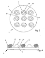
- Figure 3 shows a very schematic example of a disk-shaped substrate 5 of a sub-master 3 after recombination.
- a plurality of replication material portions 4 is shown, each comprising the inverse of a replication section 23' and of a spacer portion 24' surrounding it.
- the remaining material 27 around the spacer portion has an undefined shape and height.
- a gap 29 remains, where the substrate is not covered by replication material.
- the at least one gap is now filled before the sub-master is used in the next replication step to cast a tool from it.
- the substrate 5 - also called 'element substrate' in this text, for example has the approximate size and shape of an optical wafer, which latter is used for the final replica.
- the element substrate 5 need not necessarily be transparent.
- the filling of the gap illustrated in Figure 4 The filler material 31 fills the entire space between the replication material portions. Its height is greater than the minimal height of the replication material portions at the place of the spacer portion 24'.
- the gap is filled by a plastic material, such as an epoxy. It may be filled by material of the same composition as the replication material.
- the gap may be filled by material of a primarily metallic composition.
- the substrate 5 may be metallic or comprise a metallic surface, and the material may be added galvanically, i.e. by electroplating.
- the filling may be made of nickel or copper added by electroplating.
- the thickness of the filler material in the shown - preferred - embodiment is such that it exceeds the thickness of the replication material at the place of the spacer portions 24'. Therefore, the spacer portions of the tool cast from the sub-master protrude further than the portions at positions corresponding to the gap 29.
- Figure 5 shows a flowchart summarizing steps in a process according to the invention.
- Figure 6 shows a variant of a master tool 2' with spacer portions 32 destined to be contact spacers, i.e. in the final replication process the corresponding replicated spacers of the wafer-scale tool are to contact the substrate and to abut its surface.
- the corresponding flat spacer surface 32.1 is defined already in the master and may thus be defined very precisely.
- the cavity 33 defined by the tool and including the replication section 23 is only partially filled by replication material; it is filled at least to the extent that the space between the replication section 23 and the substrate is completely filled by the replication material.
- the replication material in the final, wafer-scale replication process is dispensed in portions, each optical element to be manufactured corresponding to one portion or to a plurality of portions.
- edges of the angled structures 35 serve as flow stops for surplus material and account for the fact that the size of the dispensed material portions may not always be defined to an extent corresponding to the accuracy of the structures themselves.
- the individual dispensing of material portions for each element and the lateral confining of replication material is described in international patent applications PCT/CH 2007/000148 and PCT/CH2007/000146 .
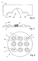
- Figure 7 shows, in analogy to Fig. 4 the manufacturing of the sub-master 3 by recombination and subsequent filling of the space between the replication material portions 4 by filler material 31.
- Figure 8 shows a variant of a sub-master 3 during a recombination process which comprises additional (in addition to the structures corresponding to the optical elements to be manufactured themselves) replicated structures.
- additional structures will, like the other structures, be replicated to the tool and from there to the final replica.
- the additional structures are alignment marks 40.
- the exact (x,y,z) positions of the alignment marks may be measured (such measurement is especially advantageous if the z position of the alignment marks will later be used, as the lateral (x,y) positions may be precisely defined by the recombination process itself).
- the alignment marks may be used for alignment.
- the alignment marks 40 to be replicated are added to the sub-master by replication, into replication material 4' some alignment mark master, this need not be the case. They may also have been added by other means. They may also be added to a wafer-scale element in an other step in the generation process than to the sub-master.
- the idea of providing on a tool or a sub-master (more in general: on a wafer-scale positive or negative copy of the elements to be finally replicated) alignment marks and of replicating them at least once to yield the final replica may be applied in combination with the idea, according to the invention, of filling spaces between replication material portions by filler material, or independently thereof.
- the gap (or space) between the regions covered by the replication material may but need not be completely covered by the filler material 31. Rather, there may be regions to be kept free of replication material, for example in a peripheral region not used for replication or where after replication special measures are applied to the tool (such as adding a holder).
- the tool element (for example master tool) does not necessarily comprise a structure corresponding to the negative copy of the surface of exactly one optical element. Rather, the tool element may encompass the (negative) structures of a few optical elements, for example of groups of four or six or nine optical elements.
Landscapes
- Engineering & Computer Science (AREA)
- Chemical & Material Sciences (AREA)
- Nanotechnology (AREA)
- Physics & Mathematics (AREA)
- Manufacturing & Machinery (AREA)
- Crystallography & Structural Chemistry (AREA)
- General Physics & Mathematics (AREA)
- Theoretical Computer Science (AREA)
- Condensed Matter Physics & Semiconductors (AREA)
- Mathematical Physics (AREA)
- Health & Medical Sciences (AREA)
- Ophthalmology & Optometry (AREA)
- Mechanical Engineering (AREA)
- Shaping Of Tube Ends By Bending Or Straightening (AREA)
- Moulds For Moulding Plastics Or The Like (AREA)
Description
- The invention is in the field of manufacturing, by replication, optical elements, in particular refractive optical elements or diffractive micro-optical elements. More concretely, it deals with a method of replicating an element and a process of manufacturing a plurality of optical elements.
- Fabrication of optical elements by replication techniques, such as embossing or molding, has been known. Of special interest are the wafer-scale fabrication processes, where an array of optical elements is fabricated on a disk-like ("wafer-") structure, which subsequently to replication is separated ("diced") into the individual elements.
- Replication techniques include injection molding, roller hot embossing, flat-bed hot embossing, UV embossing. As an example in the UV embossing process the surface topology of a master structure is duplicated into a thin film of a UV-curable replication material such as an UV curable epoxy resin on top of a substrate. The replicated surface topology can be a refractive or a diffractive optically effective structure, or a combination of both. For replicating, a tool (negative copy) is prepared from a master, which is then used to UV-emboss the epoxy resin. The master can be a lithographically fabricated structure in fused silica or silicon, a laser or e-beam written structure, a diamond turned structure or any other type of structure.
- To achieve a cost effective mass production of replicated micro-optical components, a wafer-scale replication process is desirable. A 'wafer' in the meaning used in this text is a disc or a rectangular plate of any dimensionally stable, often transparent material. The diameter of the disk is typically between 5 cm and 40 cm, for example between 10 cm and 31 cm. Often it is cylindrical with a diameter of either 2, 4, 6, 8 or 12 inches, one inch being about 2,54 cm. The wafer thickness is for example between 0,2 mm and 10 mm, typically between 0,4 mm and 6 mm. The wafer-scale replication allows the fabrication of several hundreds identical structures with a single step, e.g. a single or double-sided UV-embossing process. The subsequent separating ('dicing') step of the wafer then yields the individual micro-optical components.
- For an efficient wafer-scale replication technology a wafer-scale tool (negative copy of the replica to be manufactured) is required for fabricating the replica. Since such a waver-scale tool can only be used for a limited number of replication processes and since therefore a substantial number of wafer-scale replication tools are needed, it is also advantageous to have a wafer-scale sub-master (positive copy of the final replica to be manufactured), from which the replication tool may be cast or otherwise replicated. However, in many cases it is either not possible or very costly to directly produce a master or master tool that covers a sufficiently large area (typically at least 4 - 6 inches, up to 8 or 10 or 12 inches). For instance, mastering techniques such as e-beam writing or diamond turning typically cover only a small area in the range of several square mm which is only the size of an individual micro-optical component. Therefore, a process is required that closes the gap between the size of the individual component to the full wafer scale.
- In
WO 2005/057283 it has been proposed to manufacture a replication tool, sub-master or replica by means of a so-called recombination process. Recombination is the repeated replication of a single, small-scale structure over a large area, typically by embossing into a thermoplastic or thermosetting replication material. An embodiment of the recombination process disclosed inWO 2005/057283 relies on a so-called recombination framework, i.e., a framework of troughs into which the small-scale structure (master, sub-master or master tool) is replicated. This method features the substantial advantage that the position of the replicated structures with respect to all spatial dimensions is defined by the recombination framework. However, there are situations where a recombination framework is either not feasible, too laborious, or not suitable for the structure to be produced by the replication process. -
US 2004/0229140 A1 discloses a method of forming a color filter layer including forming a first sub-color filter on a substrate by placing a first mold having at least a first groove on the substrate and injecting a first color resin into the first groove, the substrate including first, second and third regions and the first groove corresponding to the first region. The method further includes forming a second sub-color filter on the substrate by placing a second mold having at least a second groove on the substrate and injecting a second color resin into the second groove, the second groove corresponding to the first and second regions. And the method further includes forming a third sub-color filter on the substrate by placing a third mold having at least a third groove on the substrate and injecting a third color resin into the third groove, the third groove corresponding to the first, second and third regions. -
WO 0065408 A1 - In the publication "Soft Lithography" by Y. Xia and G. M. Whitesides, Angew. Chem. Int. Ed. 1998, 37, 570-575 (Wiley-VCH Verlag, D-Weinheim, Vol:37,Page(s):551 - 575), methods of eplica molding and embossing are disclosed, in particular with elastomeric stamps and molds. A use of such methods for the manufacture of optical structures is suggested.
- In
US 2005/058948 A1 , it is suggested to fabricate microstructures by impinging a radiation beam, such as a laser beam, through a substrate that is transparent to the laser beam, into a negative photoresist layer on the substrate. The negative photoresist layer may be subsequently developed to provide a master for optical and/or mechanical microstructures. Related systems, microstructure products and microstructure masters also are disclosed. -
US 2003/217804 A1 concerns a polymer micro-ring resonator and a method of manufacturing the same that is capable of providing reduced surface roughness and improved submicron gap separation between a waveguide and a micro-ring. Nanoimprinting is employed to achieve this without the need for a final lithography and etching step. According to a first method, a hard mold is used to directly imprint a polymer film to form optical waveguides in micro-ring devices. A second method employs a template filling approach, which allows a thicker waveguide to be fabricated, as well as polymers that are difficult to directly imprint. - In
US 3 767 445 is disclosed a technique for producing integrated optical waveguides or circuits in which a substrate is embossed by a die of the desired guide pattern and is then coated with a liquid that fills the grooves and has sufficient surface tension to yield a greater thickness in the grooves than over adjacent substrate material. The liquid may be a solution of a higher-index optical material, solidifying in the grooves during evaporation of the solvent. Alternatively, a liquid monomer of a polymerizable higher-index material may be used which is subsequently polymerized in the grooves. This embossing and filling technique is particularly economical when a large number of replicas of a given optical circuit are to be produced. -
EP 1 542 074 A1 - In
US 2005/052583 A1 , a method for forming a pattern of a liquid crystal display device is disclosed. The method includes providing a substrate having a layer to be patterned, providing a master substrate having an intaglio portion corresponding to a desired pattern, filling an organic material into the intaglio portion of the master substrate, placing the master substrate in contact with the substrate, hardening the organic material to produce a hardened organic film pattern, transferring the hardened organic film pattern onto a surface of the layer to be patterned by separating the master substrate from the substrate, and etching the layer to be patterned by using the organic film pattern as a mask. -
EP 1 527 870 A2 - It is therefore an object of the invention to provide an alternative method of fabricating an element to be used in a process of manufacturing, by replication, an optical element. The element shall include a plurality of structures replicated from a prototype, and should allow for a control at least of the thickness dimension (the z-coordinate) of the final replica.
- Therefore, in a process of manufacturing, by replication, a plurality of optical elements each having geometrical surface features, a method of manufacturing an element that includes a plurality of replicated structures is provided. The method comprises the steps of providing an element substrate, of replicating, by embossing, a surface of a tool element, which surface comprises a negative copy of the geometrical surface feature, into replication material disposed at a first place on a surface of the element substrate, of subsequently hardening the replication material, of replicating said surface of the tool element into replication material disposed at a second place on said substrate, of hardening said replication material, the method comprising the further step of subsequently filling a gap between replication material disposed at the first place and replication material disposed at the second place by filler material, as it is defined in
claim 1. - The element including a plurality of replicated structures may be a 'sub-master', i.e. an element that comprises surface portions corresponding to a positive copy of a surface portion of the optical element to be replicated. The tool element may be a so-called 'master tool', i.e. an element that comprises a surface portion corresponding to a negative copy of a surface portion of the optical element to be replicated.
- The replication material may be disposed step by step, i.e. at the second place it is disposed after the replication material at the first place is hardened. According to a less preferred variant, the replication material may also be disposed at a plurality of places prior to being hardened. Then, the hardening step has to be carried out position selectively, for example by means of an appropriate mask where the hardening step includes curing a thermosetting replication material by means of illumination by electromagnetic or other radiation, such as UV radiation.
- For the sake of convenience, the dimension perpendicular to the surface of the substrate, which comprises an essentially flat surface - is denoted as "height". In actual practice, the entire arrangement may also be used in an upside down configuration or also in a configuration where the substrate surface is vertical or at an angle to the horizontal. The according direction perpendicular to the surface is denoted z-direction. The terms "periphery", "lateral" and "sides" relate to a direction perpendicular to the z-direction.
- The added filling material makes a complete control of the z-dimension of the crucial surface portions the final replica possible, even if its own thickness is not precisely controlled at all. This is because due to it the minimal thickness of the element produced may be at sections where the substrate is covered by the replication material and where the z-dimension relative to the replication section (the portion that will finally account for the desired optical properties of the optical element produced) has been defined by the replication. Such sections of minimal thickness correspond to protruding portions (spacer portions) of the tool replicated in a further replication step. They may be used to precisely define the thickness of the optical element.
- In other words, this definition of the z dimension becomes possible since the structure of the tool that protrudes the most is next to the optical structures and is defined already in the single master or master tool.
- In accordance with an other aspect of the invention, a process of manufacturing a plurality of optical elements each having surface features is provided, the process comprising the steps of providing a master or a master tool and carrying out at least a first and a second replication operation to replicate a surface portion of the master or master tool to provide a final replica, the first replication operation comprising a method of manufacturing an element including the steps of
- providing an element substrate,
- replicating, by embossing, a surface of a tool element, which surface comprises a negative copy of the geometrical surface feature, into replication material disposed at a first place on a surface of the element substrate,
- subsequently hardening the replication material,
- replicating said surface of the tool element into replication material disposed at a second place on said substrate,
- hardening said replication material,
- subsequently filling a gap between replication material disposed at the first place and replication material disposed at the second place by filler material,
- Said element may be a sub-master. The second replication material may be of the same or of a different composition than the first replication material.
- The tool by which the final replica is manufactured may in addition comprise alignment marks. The aligment marks are then added to the final replica by means of replicating the tool. The aligment marks may for example be placed at a peripheral position on the (wafer-scale) tool and may for example take the place of an element to be replicated in an array-like configuration on the tool. The aligment marks are preferably added to the sub-master or any other wafer-scale element in the generation process, by replicating an alignment mark master into replication material. Preferably, the aligment marks are added during the recombination step in the generation process.
- The invention consequently also concerns
- A process of manufacturing, by replication, a plurality of optical elements each having geometrical surface features as it is defined according to
claim 10. - In the following, preferred embodiments of the invention are described referring to schematic drawings. None of the drawings is to scale. In the drawings:
-
Fig. 1 schematically shows a generation process with a recombination step; -
Fig. 2 shows, in section, a replication tool; -
Fig. 3 shows a view of a sub-master during its manufacture; -
Fig. 4 shows, in section, a sub-master during its manufacture; -
Fig. 5 shows a flowchart of an embodiment of the method according to the invention; -
Fig. 6 shows a master tool according to an other embodiment; -
Fig. 7 shows, in section, during its manufacture, a sub-master made using the master tool ofFig. 6 ; and -
Fig. 8 shows a sub-master with replicated alignment marks. - In this text, 'replication' is used for a process of 'casting' in a broad sense, i.e. of making a 'negative' copy of a structured portion of the element to be replicated. When the resulting element is again replicated, this leads to a 'positive' copy of the initially replicated element. In this text, elements that comprise surface parts being a negative copy of portions of the final optical element to be manufactured are called 'tools', for example 'replication tool' or 'master tool'. Elements including surface portions with a positive copy of the final element to be manufactured are called 'master', 'sub-master', or, for the final copy to be diced into the optical elements, 'final replica' or 'replica'.
-
Figure 1 very schematically shows steps in a generation process for fabricating a plurality of optical elements by wafer-scale replication. In a first step, amaster 1 is produced by any suitable method, such as diamond turning or an other method. In the figure, a laser beam writing process is symbolized. In the shown embodiment, themaster 1 is replicated to yield afirst generation tool 2 or master tool. In a recombination process at least one (second generation) sub-master 3 is manufactured. The sub-master in the shown embodiment is the result of a recombination operation and includes a plurality ofportions 4 of replication material disposed at different places on asubstrate 5, and each comprising an identical replicated structure being a negative copy of the master tool structure. From each sub-master, 2ndgeneration replication tools 8 are produced which may be used for manufacturing the final replicas 10 (wafer with the micro-optical or micro-mechanical elements to be diced; dicing lines 11) or may be used for manufacturing next generation sub-masters. - In every one of the above steps not only one element but a plurality of elements may optionally be generated by replication. Thus, corresponding to an initial master, tens of master tools, hundreds of sub-masters, and thousands of replication tools may be manufactured.
- In a production process it is also possible to initially fabricate, by a mastering operation such as laser beam writing or diamond turning, a master tool, i.e. a negative copy instead of a positive copy of the element to be finally replicated. Also as an alternative, the recombination step can also be applied in any generation, depending on the needs to preserve and protect the original structure. For example, the sub-masters or even the 2nd generation replication tools may be small-dimension parts and comprise the structure to be replicated only once, so that the recombination process is used for producing the sub-master or the 2nd generation replication tools, or the replica, respectively. In other words, the recombination may be applied in the 1st, 2nd or 3rd generation etc. Also, a scale-up generation process may be envisaged, where recombination processes may be used in more than one stage, for example by using a small size master, a
medium size 1st generation replication tool, and 'large' size sub-masters or similar. - As to the replication material, in any one of the steps any suitable material which can be brought from a liquid or viscous or plastically deformable state into a state where it is dimensionally stable can be used. As an example, the replication material may be an epoxy, such as a UV curable epoxy. As a second example, the replication material may be PDMS. The replication material may but need not be identical for the different replication steps. Except for the final replication (depending on the nature of the optical element replicated), the replication material need not be transparent.
- The replication process may be an embossing process or an other cast process. An example of such an other cast process is described in
WO 2004/068198 with reference to Figures 14-16. - In the embodiment of the generation process described with respect to
Figure 1 , there remain gaps 7 between theportions 4 of replication material. If in the subsequent replication step the replication material is dispersed on thesubstrate 9, these gaps produce protrusions 8.1 in the negative copy. These protrusions 8.1, the height of which is not defined by the mastering process but is only defined to the extent that the distance between themaster tool 2 and thesubstrate 5 in the replication steps of the recombination process is defined. This may be disadvantageous if spacer portions are used. - An example of a
replication tool 21 for wafer-scale replication (as corresponding to the last step in the above-described generation process), which replication tool comprisesspacer portions 24 is shown in section inFigure 2 . - The
replication tool 21 comprises a plurality ofreplication sections 23 i.e. negative structural features defining the shape of elements to be created with the tool. In the figure, a simple shape for a refractive optical element is shown, however, it is also possible to provide more sophisticated structures for refractive and/or diffractive optical elements. The replication tool further comprisesspacer portions 24. Thespacer portions 24 may at least partially surround thereplication sections 23. The replication tool further comprisesspill zones 26 for excess replication material. In the shown embodiment, the spill zones are located around the dicing lines, i.e. the lines where after replication, hardening and removing the replication tool the substrate with hardened replication material is separated into individual parts, is finally to be separated into the individual optical components. This need not be the case. Rather, spacer portions may cover the dicing lines, as has been described in theU.S. patent application 11/384,558 - At least some of the spacer portions may, during replication, abut the substrate. In addition or as an alternative, at least some of the spacer portions may be 'floating', i.e. a thin base layer of replication material may remain between the spacer portions and the substrate during final replication. The purpose of the spacer portions is one or a combination of the following:
- The spacer portions precisely determine a reference height of the replicated structures above the substrate.
- The spacer portions may absorb at least part of the force between the tool and substrate during replication.
- The spacer portions also allow the tool to adapt to irregularities of the planarity of the substrate.
- Spacer portions arranged along the dicing lines help to prevent delaminating of the replication material from the substrate.
- The
replication tool 21 further comprises arigid back plate 22 to make it dimensionally stiff on a large scale. - As an alternative to the shown embodiment, the replication tool may be designed in accordance with the teaching of the international application publication
WO 2004/068 198 and/or of any one of theU.S. applications 11/384,56211/384,537 11/384,563 11/384,558 -
Figure 3 shows a very schematic example of a disk-shapedsubstrate 5 of asub-master 3 after recombination. On the substrate, a plurality ofreplication material portions 4 is shown, each comprising the inverse of a replication section 23' and of a spacer portion 24' surrounding it. The remainingmaterial 27 around the spacer portion has an undefined shape and height. Between thereplication material portions 4, agap 29 remains, where the substrate is not covered by replication material. In accordance with the invention, the at least one gap is now filled before the sub-master is used in the next replication step to cast a tool from it. - The substrate 5 - also called 'element substrate' in this text, for example has the approximate size and shape of an optical wafer, which latter is used for the final replica. However, in contrast to the optical wafer, the
element substrate 5 need not necessarily be transparent. - The filling of the gap illustrated in
Figure 4 . Thefiller material 31 fills the entire space between the replication material portions. Its height is greater than the minimal height of the replication material portions at the place of the spacer portion 24'. - In accordance with a first embodiment, the gap is filled by a plastic material, such as an epoxy. It may be filled by material of the same composition as the replication material.
- According to a second embodiment, the gap may be filled by material of a primarily metallic composition. Especially, the
substrate 5 may be metallic or comprise a metallic surface, and the material may be added galvanically, i.e. by electroplating. For example, the filling may be made of nickel or copper added by electroplating. - Other variants of filling the gap may be envisaged.
- The thickness of the filler material in the shown - preferred - embodiment is such that it exceeds the thickness of the replication material at the place of the spacer portions 24'. Therefore, the spacer portions of the tool cast from the sub-master protrude further than the portions at positions corresponding to the
gap 29. -
Figure 5 shows a flowchart summarizing steps in a process according to the invention. -
Figure 6 shows a variant of a master tool 2' withspacer portions 32 destined to be contact spacers, i.e. in the final replication process the corresponding replicated spacers of the wafer-scale tool are to contact the substrate and to abut its surface. The corresponding flat spacer surface 32.1 is defined already in the master and may thus be defined very precisely. In the final replication process, thecavity 33 defined by the tool and including thereplication section 23 is only partially filled by replication material; it is filled at least to the extent that the space between thereplication section 23 and the substrate is completely filled by the replication material. To do so, the replication material in the final, wafer-scale replication process is dispensed in portions, each optical element to be manufactured corresponding to one portion or to a plurality of portions. The edges of the angled structures 35 serve as flow stops for surplus material and account for the fact that the size of the dispensed material portions may not always be defined to an extent corresponding to the accuracy of the structures themselves. The individual dispensing of material portions for each element and the lateral confining of replication material is described in international patent applicationsPCT/CH 2007/000148 PCT/CH2007/000146 - Also the variant of
Figure 6 , the advantages of the invention are evident. The flat surface 32.1 of the spacers that is very precisely defined will, due to the approach according to the invention, eventually define the height of the final replica elements (which are for example lenses), and thus the optical properties. -
Figure 7 shows, in analogy toFig. 4 the manufacturing of thesub-master 3 by recombination and subsequent filling of the space between thereplication material portions 4 byfiller material 31. -
Figure 8 shows a variant of asub-master 3 during a recombination process which comprises additional (in addition to the structures corresponding to the optical elements to be manufactured themselves) replicated structures. These additional structures will, like the other structures, be replicated to the tool and from there to the final replica. In the shown embodiment, the additional structures are alignment marks 40. Subsequently to the recombination process, the exact (x,y,z) positions of the alignment marks may be measured (such measurement is especially advantageous if the z position of the alignment marks will later be used, as the lateral (x,y) positions may be precisely defined by the recombination process itself). In the final replication step (for example in the case of two-sided replication) or thereafter (for alignment of different wafers in a stack of wafers), the alignment marks may be used for alignment. - Whereas preferably like in the shown embodiment the alignment marks 40 to be replicated are added to the sub-master by replication, into replication material 4' some alignment mark master, this need not be the case. They may also have been added by other means. They may also be added to a wafer-scale element in an other step in the generation process than to the sub-master.
- The idea of providing on a tool or a sub-master (more in general: on a wafer-scale positive or negative copy of the elements to be finally replicated) alignment marks and of replicating them at least once to yield the final replica may be applied in combination with the idea, according to the invention, of filling spaces between replication material portions by filler material, or independently thereof.
- The gap (or space) between the regions covered by the replication material may but need not be completely covered by the
filler material 31. Rather, there may be regions to be kept free of replication material, for example in a peripheral region not used for replication or where after replication special measures are applied to the tool (such as adding a holder). - As a further variant, the tool element (for example master tool) does not necessarily comprise a structure corresponding to the negative copy of the surface of exactly one optical element. Rather, the tool element may encompass the (negative) structures of a few optical elements, for example of groups of four or six or nine optical elements.
- Various other embodiments may be envisaged without departing from the scope of the invention.
Claims (10)
- A method of manufacturing an element that includes a plurality of replicated structures for being used in a process of manufacturing, by replication, a plurality of optical elements each having geometrical surface features, the method comprising the steps of- providing an element substrate,- replicating, by embossing, a surface of a tool element, which surface comprises a negative copy of the geometrical surface feature, into first replication material disposed at a first place on a surface of the element substrate,- subsequently hardening the first replication material,- replicating said surface of the tool element into first replication material disposed at a second place on said element substrate,- subsequently hardening said first replication material,
the method comprising the further step of- subsequently filling a gap between first replication material disposed at the first place and first replication material disposed at the second place by filler material. - The method according to claim 1, wherein the gap between regions of material with replicated structures is filled to an extent that the thickness of the filler material is greater than a minimal thickness of material in the regions of replicated material.
- The method according to claim 2, wherein master tool has a replicating surface which comprises flat sections where the height of the replicating surface is at a maximum, so that said flat sections define a region where the minimal thickness of the material with replicated structures is attained.
- The method according to any one of the previous claims, wherein the filler material is a curable plastic material.
- The method according to claim 4, wherein the filler material is a material of the same composition as the first replication material.
- The method according to any one of the previous claims, wherein the element substrate comprises an electrically conductive surface portion and wherein the filler material is applied galvanically.
- The method according to any one of the previous claims, wherein the element substrate has the size and shape of an optical wafer.
- The method according to claim 1, wherein said surface of the tool element is, in consecutive sub-steps replicated into first replication material disposed at at least 40 places on said element substrate and wherein gaps between first replication material disposed at different places are filled by the filler material in a single step.
- A process of manufacturing a plurality of optical elements each having surface features, the process comprising the steps of providing a master or a master tool and carrying out at least a first and a second replication operation to provide a final replica comprising surface portions being a positive or negative copy of a surface portion of the master or master tool, the first replication operation comprising a method of manufacturing an element according to claim 1, the second replication operation including the steps of providing a second substrate and a second replication material disposed between the second substrate and said element, of moving the substrate and said element against each other, and of hardening the second replication material.
- A process according to claim 9, of manufacturing, by replication, a plurality of optical elements each having geometrical surface features, the process comprising the steps of- providing an element substrate,- replicating, by embossing, a surface of a replication tool, which surface comprises a negative copy of the geometrical surface feature, into replication material disposed between said substrate and said replication tool,- subsequently hardening the replication material, and- removing the replication tool, the replication material remaining attached to the substrate,wherein the replication tool comprises alignment marks, and wherein said alignment marks are replicated into said replication material.
Applications Claiming Priority (2)
| Application Number | Priority Date | Filing Date | Title |
|---|---|---|---|
| US11/423,344 US20100072640A1 (en) | 2006-06-09 | 2006-06-09 | Manufacturing a replication tool, sub-master or replica |
| PCT/CH2007/000283 WO2007140643A1 (en) | 2006-06-09 | 2007-06-06 | Manufacturing a replication tool |
Publications (2)
| Publication Number | Publication Date |
|---|---|
| EP2033050A1 EP2033050A1 (en) | 2009-03-11 |
| EP2033050B1 true EP2033050B1 (en) | 2013-02-27 |
Family
ID=38292769
Family Applications (1)
| Application Number | Title | Priority Date | Filing Date |
|---|---|---|---|
| EP07720180A Not-in-force EP2033050B1 (en) | 2006-06-09 | 2007-06-06 | Manufacturing a replication tool |
Country Status (4)
| Country | Link |
|---|---|
| US (1) | US20100072640A1 (en) |
| EP (1) | EP2033050B1 (en) |
| TW (1) | TWI421629B (en) |
| WO (1) | WO2007140643A1 (en) |
Families Citing this family (9)
| Publication number | Priority date | Publication date | Assignee | Title |
|---|---|---|---|---|
| TWI421162B (en) * | 2008-11-03 | 2014-01-01 | Molecular Imprints Inc | Master template replication |
| SG10201701641RA (en) | 2012-09-11 | 2017-04-27 | Heptagon Micro Optics Pte Ltd | Manufacture of truncated lenses, of pairs of truncated lenses and of corresponding devices |
| US8606057B1 (en) | 2012-11-02 | 2013-12-10 | Heptagon Micro Optics Pte. Ltd. | Opto-electronic modules including electrically conductive connections for integration with an electronic device |
| US20170090294A1 (en) * | 2015-09-29 | 2017-03-30 | Apple Inc. | High-volume replication of diffractive optical elements |
| WO2018208229A1 (en) * | 2017-05-09 | 2018-11-15 | Heptagon Micro Optics Pte. Ltd. | Method for conditioning a replication tool and related method for manufacturing a multitude of devices |
| CN113939771A (en) | 2019-05-31 | 2022-01-14 | ams传感器新加坡私人有限公司 | Method of manufacturing a master for a replication process |
| CN116089432B (en) | 2020-05-29 | 2026-01-02 | 斯诺弗雷克公司 | Methods and systems for implementing sub-table copying, and computer-readable storage media |
| US10997210B1 (en) * | 2020-05-29 | 2021-05-04 | Snowflake Inc. | System for implementing sub-database replication |
| WO2021255007A1 (en) * | 2020-06-16 | 2021-12-23 | Nilt Switzerland Gmbh | Surface treatment for replication |
Family Cites Families (19)
| Publication number | Priority date | Publication date | Assignee | Title |
|---|---|---|---|---|
| US3767445A (en) * | 1971-10-14 | 1973-10-23 | Bell Telephone Labor Inc | Embossing techniques for producing integrated optical circuits |
| US4197266A (en) * | 1974-05-06 | 1980-04-08 | Bausch & Lomb Incorporated | Method for forming optical lenses |
| US5174937A (en) * | 1987-09-05 | 1992-12-29 | Canon Kabushiki Kaisha | Method for molding of substrate for information recording medium and method for preparing substrate for information recording medium |
| US5536455A (en) * | 1994-01-03 | 1996-07-16 | Omron Corporation | Method of manufacturing lens array |
| US6297911B1 (en) * | 1998-08-27 | 2001-10-02 | Seiko Epson Corporation | Micro lens array, method of fabricating the same, and display device |
| KR100335070B1 (en) * | 1999-04-21 | 2002-05-03 | 백승준 | Method for forming micro pattern on substrate by using compression patterning technique |
| US6805902B1 (en) * | 2000-02-28 | 2004-10-19 | Microfab Technologies, Inc. | Precision micro-optical elements and the method of making precision micro-optical elements |
| JP2002122707A (en) * | 2000-10-13 | 2002-04-26 | Canon Inc | Aspherical microstructure and method of manufacturing the same |
| JP2002205312A (en) * | 2000-11-10 | 2002-07-23 | Dainippon Printing Co Ltd | Method and apparatus for manufacturing lens sheet |
| US6894840B2 (en) * | 2002-05-13 | 2005-05-17 | Sony Corporation | Production method of microlens array, liquid crystal display device and production method thereof, and projector |
| US20030217804A1 (en) * | 2002-05-24 | 2003-11-27 | Guo Lingjie J. | Polymer micro-ring resonator device and fabrication method |
| US7195732B2 (en) * | 2002-09-18 | 2007-03-27 | Ricoh Optical Industries Co., Ltd. | Method and mold for fabricating article having fine surface structure |
| EP1443344A1 (en) * | 2003-01-29 | 2004-08-04 | Heptagon Oy | Manufacturing micro-structured elements |
| KR100911421B1 (en) * | 2003-05-16 | 2009-08-11 | 엘지디스플레이 주식회사 | Color filter forming method using mold and liquid crystal display device manufacturing method including the same |
| KR100675632B1 (en) * | 2003-09-08 | 2007-02-01 | 엘지.필립스 엘시디 주식회사 | Pattern Forming Method and Manufacturing Method of Liquid Crystal Display Using The Same |
| US7867695B2 (en) * | 2003-09-11 | 2011-01-11 | Bright View Technologies Corporation | Methods for mastering microstructures through a substrate using negative photoresist |
| US7094304B2 (en) * | 2003-10-31 | 2006-08-22 | Agilent Technologies, Inc. | Method for selective area stamping of optical elements on a substrate |
| EP1542074A1 (en) * | 2003-12-11 | 2005-06-15 | Heptagon OY | Manufacturing a replication tool, sub-master or replica |
| JP5128047B2 (en) * | 2004-10-07 | 2013-01-23 | Towa株式会社 | Optical device and optical device production method |
-
2006
- 2006-06-09 US US11/423,344 patent/US20100072640A1/en not_active Abandoned
-
2007
- 2007-06-06 EP EP07720180A patent/EP2033050B1/en not_active Not-in-force
- 2007-06-06 WO PCT/CH2007/000283 patent/WO2007140643A1/en not_active Ceased
- 2007-06-07 TW TW096120538A patent/TWI421629B/en not_active IP Right Cessation
Also Published As
| Publication number | Publication date |
|---|---|
| TWI421629B (en) | 2014-01-01 |
| EP2033050A1 (en) | 2009-03-11 |
| WO2007140643A1 (en) | 2007-12-13 |
| US20100072640A1 (en) | 2010-03-25 |
| TW200817834A (en) | 2008-04-16 |
Similar Documents
| Publication | Publication Date | Title |
|---|---|---|
| US7658877B2 (en) | Manufacturing micro-structured elements | |
| EP1959299B1 (en) | Pattern replication with intermediate stamp | |
| EP1594001B1 (en) | Device and method for imprint lithography | |
| US8221665B2 (en) | Manufacturing a replication tool, sub-master or replica | |
| JP7532260B2 (en) | Wafer tiling method to form large area die masters with submicron features - Patents.com | |
| US20050162733A1 (en) | Method of fabricating diffractive lens array and UV dispenser used therein | |
| TWI421629B (en) | Method of making a copying tool, a submaster or a replica | |
| EP2225096B1 (en) | Manufacturing optical elements | |
| US20170090294A1 (en) | High-volume replication of diffractive optical elements | |
| KR100930925B1 (en) | Composite Imprint Stamp and Manufacturing Method | |
| HK1086071B (en) | Manufacturing micro-structured elements | |
| EP1378341A2 (en) | Method of producing a deep microrelief optical element | |
| WO2020185162A1 (en) | Method of manufacturing a plurality of optical elements and product thereof | |
| HK40043224A (en) | Wafer tiling method to form large-area mold master having sub-micrometer features | |
| HK1121243B (en) | Pattern replication with intermediate stamp | |
| HK1096162B (en) | Pattern replication with intermediate stamp |
Legal Events
| Date | Code | Title | Description |
|---|---|---|---|
| PUAI | Public reference made under article 153(3) epc to a published international application that has entered the european phase |
Free format text: ORIGINAL CODE: 0009012 |
|
| 17P | Request for examination filed |
Effective date: 20081212 |
|
| AK | Designated contracting states |
Kind code of ref document: A1 Designated state(s): AT BE BG CH CY CZ DE DK EE ES FI FR GB GR HU IE IS IT LI LT LU LV MC MT NL PL PT RO SE SI SK TR |
|
| AX | Request for extension of the european patent |
Extension state: AL BA HR MK RS |
|
| 17Q | First examination report despatched |
Effective date: 20110411 |
|
| DAX | Request for extension of the european patent (deleted) | ||
| GRAP | Despatch of communication of intention to grant a patent |
Free format text: ORIGINAL CODE: EPIDOSNIGR1 |
|
| RAP1 | Party data changed (applicant data changed or rights of an application transferred) |
Owner name: HEPTAGON MICRO OPTICS PTE. LTD. |
|
| GRAS | Grant fee paid |
Free format text: ORIGINAL CODE: EPIDOSNIGR3 |
|
| GRAA | (expected) grant |
Free format text: ORIGINAL CODE: 0009210 |
|
| AK | Designated contracting states |
Kind code of ref document: B1 Designated state(s): AT BE BG CH CY CZ DE DK EE ES FI FR GB GR HU IE IS IT LI LT LU LV MC MT NL PL PT RO SE SI SK TR |
|
| REG | Reference to a national code |
Ref country code: GB Ref legal event code: FG4D |
|
| REG | Reference to a national code |
Ref country code: CH Ref legal event code: EP |
|
| REG | Reference to a national code |
Ref country code: AT Ref legal event code: REF Ref document number: 598792 Country of ref document: AT Kind code of ref document: T Effective date: 20130315 |
|
| REG | Reference to a national code |
Ref country code: IE Ref legal event code: FG4D |
|
| REG | Reference to a national code |
Ref country code: DE Ref legal event code: R096 Ref document number: 602007028697 Country of ref document: DE Effective date: 20130425 |
|
| REG | Reference to a national code |
Ref country code: AT Ref legal event code: MK05 Ref document number: 598792 Country of ref document: AT Kind code of ref document: T Effective date: 20130227 |
|
| REG | Reference to a national code |
Ref country code: NL Ref legal event code: T3 |
|
| REG | Reference to a national code |
Ref country code: LT Ref legal event code: MG4D |
|
| PG25 | Lapsed in a contracting state [announced via postgrant information from national office to epo] |
Ref country code: SE Free format text: LAPSE BECAUSE OF FAILURE TO SUBMIT A TRANSLATION OF THE DESCRIPTION OR TO PAY THE FEE WITHIN THE PRESCRIBED TIME-LIMIT Effective date: 20130227 Ref country code: ES Free format text: LAPSE BECAUSE OF FAILURE TO SUBMIT A TRANSLATION OF THE DESCRIPTION OR TO PAY THE FEE WITHIN THE PRESCRIBED TIME-LIMIT Effective date: 20130607 Ref country code: IS Free format text: LAPSE BECAUSE OF FAILURE TO SUBMIT A TRANSLATION OF THE DESCRIPTION OR TO PAY THE FEE WITHIN THE PRESCRIBED TIME-LIMIT Effective date: 20130627 Ref country code: AT Free format text: LAPSE BECAUSE OF FAILURE TO SUBMIT A TRANSLATION OF THE DESCRIPTION OR TO PAY THE FEE WITHIN THE PRESCRIBED TIME-LIMIT Effective date: 20130227 Ref country code: BG Free format text: LAPSE BECAUSE OF FAILURE TO SUBMIT A TRANSLATION OF THE DESCRIPTION OR TO PAY THE FEE WITHIN THE PRESCRIBED TIME-LIMIT Effective date: 20130527 Ref country code: LT Free format text: LAPSE BECAUSE OF FAILURE TO SUBMIT A TRANSLATION OF THE DESCRIPTION OR TO PAY THE FEE WITHIN THE PRESCRIBED TIME-LIMIT Effective date: 20130227 |
|
| PG25 | Lapsed in a contracting state [announced via postgrant information from national office to epo] |
Ref country code: PL Free format text: LAPSE BECAUSE OF FAILURE TO SUBMIT A TRANSLATION OF THE DESCRIPTION OR TO PAY THE FEE WITHIN THE PRESCRIBED TIME-LIMIT Effective date: 20130227 Ref country code: GR Free format text: LAPSE BECAUSE OF FAILURE TO SUBMIT A TRANSLATION OF THE DESCRIPTION OR TO PAY THE FEE WITHIN THE PRESCRIBED TIME-LIMIT Effective date: 20130528 Ref country code: LV Free format text: LAPSE BECAUSE OF FAILURE TO SUBMIT A TRANSLATION OF THE DESCRIPTION OR TO PAY THE FEE WITHIN THE PRESCRIBED TIME-LIMIT Effective date: 20130227 Ref country code: SI Free format text: LAPSE BECAUSE OF FAILURE TO SUBMIT A TRANSLATION OF THE DESCRIPTION OR TO PAY THE FEE WITHIN THE PRESCRIBED TIME-LIMIT Effective date: 20130227 Ref country code: BE Free format text: LAPSE BECAUSE OF FAILURE TO SUBMIT A TRANSLATION OF THE DESCRIPTION OR TO PAY THE FEE WITHIN THE PRESCRIBED TIME-LIMIT Effective date: 20130227 Ref country code: PT Free format text: LAPSE BECAUSE OF FAILURE TO SUBMIT A TRANSLATION OF THE DESCRIPTION OR TO PAY THE FEE WITHIN THE PRESCRIBED TIME-LIMIT Effective date: 20130627 |
|
| PG25 | Lapsed in a contracting state [announced via postgrant information from national office to epo] |
Ref country code: EE Free format text: LAPSE BECAUSE OF FAILURE TO SUBMIT A TRANSLATION OF THE DESCRIPTION OR TO PAY THE FEE WITHIN THE PRESCRIBED TIME-LIMIT Effective date: 20130227 Ref country code: DK Free format text: LAPSE BECAUSE OF FAILURE TO SUBMIT A TRANSLATION OF THE DESCRIPTION OR TO PAY THE FEE WITHIN THE PRESCRIBED TIME-LIMIT Effective date: 20130227 Ref country code: SK Free format text: LAPSE BECAUSE OF FAILURE TO SUBMIT A TRANSLATION OF THE DESCRIPTION OR TO PAY THE FEE WITHIN THE PRESCRIBED TIME-LIMIT Effective date: 20130227 Ref country code: RO Free format text: LAPSE BECAUSE OF FAILURE TO SUBMIT A TRANSLATION OF THE DESCRIPTION OR TO PAY THE FEE WITHIN THE PRESCRIBED TIME-LIMIT Effective date: 20130227 Ref country code: CZ Free format text: LAPSE BECAUSE OF FAILURE TO SUBMIT A TRANSLATION OF THE DESCRIPTION OR TO PAY THE FEE WITHIN THE PRESCRIBED TIME-LIMIT Effective date: 20130227 |
|
| PG25 | Lapsed in a contracting state [announced via postgrant information from national office to epo] |
Ref country code: CY Free format text: LAPSE BECAUSE OF FAILURE TO SUBMIT A TRANSLATION OF THE DESCRIPTION OR TO PAY THE FEE WITHIN THE PRESCRIBED TIME-LIMIT Effective date: 20130227 |
|
| PG25 | Lapsed in a contracting state [announced via postgrant information from national office to epo] |
Ref country code: IT Free format text: LAPSE BECAUSE OF FAILURE TO SUBMIT A TRANSLATION OF THE DESCRIPTION OR TO PAY THE FEE WITHIN THE PRESCRIBED TIME-LIMIT Effective date: 20130227 |
|
| PLBE | No opposition filed within time limit |
Free format text: ORIGINAL CODE: 0009261 |
|
| STAA | Information on the status of an ep patent application or granted ep patent |
Free format text: STATUS: NO OPPOSITION FILED WITHIN TIME LIMIT |
|
| PG25 | Lapsed in a contracting state [announced via postgrant information from national office to epo] |
Ref country code: MC Free format text: LAPSE BECAUSE OF FAILURE TO SUBMIT A TRANSLATION OF THE DESCRIPTION OR TO PAY THE FEE WITHIN THE PRESCRIBED TIME-LIMIT Effective date: 20130227 |
|
| REG | Reference to a national code |
Ref country code: CH Ref legal event code: PL |
|
| 26N | No opposition filed |
Effective date: 20131128 |
|
| REG | Reference to a national code |
Ref country code: DE Ref legal event code: R097 Ref document number: 602007028697 Country of ref document: DE Effective date: 20131128 |
|
| REG | Reference to a national code |
Ref country code: IE Ref legal event code: MM4A |
|
| PG25 | Lapsed in a contracting state [announced via postgrant information from national office to epo] |
Ref country code: LI Free format text: LAPSE BECAUSE OF NON-PAYMENT OF DUE FEES Effective date: 20130630 Ref country code: IE Free format text: LAPSE BECAUSE OF NON-PAYMENT OF DUE FEES Effective date: 20130606 Ref country code: CH Free format text: LAPSE BECAUSE OF NON-PAYMENT OF DUE FEES Effective date: 20130630 |
|
| PG25 | Lapsed in a contracting state [announced via postgrant information from national office to epo] |
Ref country code: MT Free format text: LAPSE BECAUSE OF FAILURE TO SUBMIT A TRANSLATION OF THE DESCRIPTION OR TO PAY THE FEE WITHIN THE PRESCRIBED TIME-LIMIT Effective date: 20130227 |
|
| PG25 | Lapsed in a contracting state [announced via postgrant information from national office to epo] |
Ref country code: TR Free format text: LAPSE BECAUSE OF FAILURE TO SUBMIT A TRANSLATION OF THE DESCRIPTION OR TO PAY THE FEE WITHIN THE PRESCRIBED TIME-LIMIT Effective date: 20130227 |
|
| PG25 | Lapsed in a contracting state [announced via postgrant information from national office to epo] |
Ref country code: HU Free format text: LAPSE BECAUSE OF FAILURE TO SUBMIT A TRANSLATION OF THE DESCRIPTION OR TO PAY THE FEE WITHIN THE PRESCRIBED TIME-LIMIT; INVALID AB INITIO Effective date: 20070606 Ref country code: LU Free format text: LAPSE BECAUSE OF NON-PAYMENT OF DUE FEES Effective date: 20130606 |
|
| REG | Reference to a national code |
Ref country code: FR Ref legal event code: PLFP Year of fee payment: 10 |
|
| REG | Reference to a national code |
Ref country code: FR Ref legal event code: PLFP Year of fee payment: 11 |
|
| REG | Reference to a national code |
Ref country code: FR Ref legal event code: PLFP Year of fee payment: 12 |
|
| REG | Reference to a national code |
Ref country code: DE Ref legal event code: R082 Ref document number: 602007028697 Country of ref document: DE Representative=s name: VIERING, JENTSCHURA & PARTNER MBB PATENT- UND , DE Ref country code: DE Ref legal event code: R082 Ref document number: 602007028697 Country of ref document: DE Representative=s name: PROCK, THOMAS, DR., GB |
|
| PGFP | Annual fee paid to national office [announced via postgrant information from national office to epo] |
Ref country code: NL Payment date: 20230620 Year of fee payment: 17 Ref country code: FR Payment date: 20230627 Year of fee payment: 17 Ref country code: DE Payment date: 20230620 Year of fee payment: 17 |
|
| PGFP | Annual fee paid to national office [announced via postgrant information from national office to epo] |
Ref country code: FI Payment date: 20230621 Year of fee payment: 17 |
|
| P01 | Opt-out of the competence of the unified patent court (upc) registered |
Effective date: 20230825 |
|
| PGFP | Annual fee paid to national office [announced via postgrant information from national office to epo] |
Ref country code: GB Payment date: 20230620 Year of fee payment: 17 |
|
| REG | Reference to a national code |
Ref country code: DE Ref legal event code: R081 Ref document number: 602007028697 Country of ref document: DE Owner name: AMS-OSRAM ASIA PACIFIC PTE. LTD., SG Free format text: FORMER OWNER: HEPTAGON MICRO OPTICS PTE. LTD., SINGAPORE, SG |
|
| REG | Reference to a national code |
Ref country code: DE Ref legal event code: R082 Ref document number: 602007028697 Country of ref document: DE Representative=s name: VIERING, JENTSCHURA & PARTNER MBB PATENT- UND , DE |
|
| REG | Reference to a national code |
Ref country code: NL Ref legal event code: HC Owner name: AMS-OSRAM ASIA PACIFIC PTE. LTD.; SG Free format text: DETAILS ASSIGNMENT: CHANGE OF OWNER(S), CHANGE OF OWNER(S) NAME; FORMER OWNER NAME: HEPTAGON MICRO OPTICS PTE. LTD. Effective date: 20241113 |
|
| REG | Reference to a national code |
Ref country code: DE Ref legal event code: R119 Ref document number: 602007028697 Country of ref document: DE |
|
| PG25 | Lapsed in a contracting state [announced via postgrant information from national office to epo] |
Ref country code: FI Free format text: LAPSE BECAUSE OF NON-PAYMENT OF DUE FEES Effective date: 20240606 |
|
| PG25 | Lapsed in a contracting state [announced via postgrant information from national office to epo] |
Ref country code: FI Free format text: LAPSE BECAUSE OF NON-PAYMENT OF DUE FEES Effective date: 20240606 |
|
| REG | Reference to a national code |
Ref country code: NL Ref legal event code: MM Effective date: 20240701 |
|
| GBPC | Gb: european patent ceased through non-payment of renewal fee |
Effective date: 20240606 |
|
| PG25 | Lapsed in a contracting state [announced via postgrant information from national office to epo] |
Ref country code: NL Free format text: LAPSE BECAUSE OF NON-PAYMENT OF DUE FEES Effective date: 20240701 |
|
| PG25 | Lapsed in a contracting state [announced via postgrant information from national office to epo] |
Ref country code: NL Free format text: LAPSE BECAUSE OF NON-PAYMENT OF DUE FEES Effective date: 20240701 |
|
| PG25 | Lapsed in a contracting state [announced via postgrant information from national office to epo] |
Ref country code: DE Free format text: LAPSE BECAUSE OF NON-PAYMENT OF DUE FEES Effective date: 20250101 |
|
| PG25 | Lapsed in a contracting state [announced via postgrant information from national office to epo] |
Ref country code: FR Free format text: LAPSE BECAUSE OF NON-PAYMENT OF DUE FEES Effective date: 20240630 |
|
| PG25 | Lapsed in a contracting state [announced via postgrant information from national office to epo] |
Ref country code: GB Free format text: LAPSE BECAUSE OF NON-PAYMENT OF DUE FEES Effective date: 20240606 |