EP2028703A2 - Herstellung einer piezoelektrischen einkristallinen Dünnschicht auf einem Siliziumwafer - Google Patents
Herstellung einer piezoelektrischen einkristallinen Dünnschicht auf einem Siliziumwafer Download PDFInfo
- Publication number
- EP2028703A2 EP2028703A2 EP08162225A EP08162225A EP2028703A2 EP 2028703 A2 EP2028703 A2 EP 2028703A2 EP 08162225 A EP08162225 A EP 08162225A EP 08162225 A EP08162225 A EP 08162225A EP 2028703 A2 EP2028703 A2 EP 2028703A2
- Authority
- EP
- European Patent Office
- Prior art keywords
- piezoelectric
- wafer
- silicon wafer
- silicon
- fabricating
- Prior art date
- Legal status (The legal status is an assumption and is not a legal conclusion. Google has not performed a legal analysis and makes no representation as to the accuracy of the status listed.)
- Withdrawn
Links
- 229910052710 silicon Inorganic materials 0.000 title claims abstract description 47
- 239000010703 silicon Substances 0.000 title claims abstract description 47
- 238000004519 manufacturing process Methods 0.000 title claims abstract description 11
- XUIMIQQOPSSXEZ-UHFFFAOYSA-N Silicon Chemical compound [Si] XUIMIQQOPSSXEZ-UHFFFAOYSA-N 0.000 title claims description 28
- 239000013078 crystal Substances 0.000 claims description 11
- 229910003781 PbTiO3 Inorganic materials 0.000 claims description 6
- 238000005498 polishing Methods 0.000 claims description 6
- 239000000126 substance Substances 0.000 claims description 6
- 238000004026 adhesive bonding Methods 0.000 claims description 5
- 238000000227 grinding Methods 0.000 claims description 4
- 239000004593 Epoxy Substances 0.000 claims description 3
- 229910004243 O3-PbTiO3 Inorganic materials 0.000 claims description 3
- 229910004293 O3—PbTiO3 Inorganic materials 0.000 claims description 3
- ISWSIDIOOBJBQZ-UHFFFAOYSA-N Phenol Chemical compound OC1=CC=CC=C1 ISWSIDIOOBJBQZ-UHFFFAOYSA-N 0.000 claims description 3
- 238000000151 deposition Methods 0.000 claims description 3
- 239000005007 epoxy-phenolic resin Substances 0.000 claims description 3
- 238000001039 wet etching Methods 0.000 claims description 3
- 229910020215 Pb(Mg1/3Nb2/3)O3PbTiO3 Inorganic materials 0.000 claims description 2
- 229910010252 TiO3 Inorganic materials 0.000 claims description 2
- 230000005496 eutectics Effects 0.000 claims description 2
- 238000009472 formulation Methods 0.000 claims description 2
- 239000000203 mixture Substances 0.000 claims description 2
- 238000005476 soldering Methods 0.000 claims description 2
- 235000012431 wafers Nutrition 0.000 abstract description 47
- 238000005459 micromachining Methods 0.000 abstract description 2
- 238000000034 method Methods 0.000 description 8
- 239000000523 sample Substances 0.000 description 7
- VYPSYNLAJGMNEJ-UHFFFAOYSA-N Silicium dioxide Chemical compound O=[Si]=O VYPSYNLAJGMNEJ-UHFFFAOYSA-N 0.000 description 6
- 238000003384 imaging method Methods 0.000 description 6
- 238000005530 etching Methods 0.000 description 4
- 229910052581 Si3N4 Inorganic materials 0.000 description 3
- 239000000853 adhesive Substances 0.000 description 3
- 230000001070 adhesive effect Effects 0.000 description 3
- 229910052681 coesite Inorganic materials 0.000 description 3
- 229910052906 cristobalite Inorganic materials 0.000 description 3
- 238000005259 measurement Methods 0.000 description 3
- 230000004044 response Effects 0.000 description 3
- 239000000377 silicon dioxide Substances 0.000 description 3
- 229910052682 stishovite Inorganic materials 0.000 description 3
- 229910052905 tridymite Inorganic materials 0.000 description 3
- -1 Sc3+ Chemical compound 0.000 description 2
- 230000008878 coupling Effects 0.000 description 2
- 238000010168 coupling process Methods 0.000 description 2
- 238000005859 coupling reaction Methods 0.000 description 2
- 239000003822 epoxy resin Substances 0.000 description 2
- 239000011521 glass Substances 0.000 description 2
- 239000012528 membrane Substances 0.000 description 2
- 239000003921 oil Substances 0.000 description 2
- 229920000647 polyepoxide Polymers 0.000 description 2
- 238000002360 preparation method Methods 0.000 description 2
- 230000008569 process Effects 0.000 description 2
- 238000012545 processing Methods 0.000 description 2
- 238000004088 simulation Methods 0.000 description 2
- 238000001228 spectrum Methods 0.000 description 2
- 238000004544 sputter deposition Methods 0.000 description 2
- 239000000758 substrate Substances 0.000 description 2
- 239000002033 PVDF binder Substances 0.000 description 1
- 229910020231 Pb(Mg1/3Nb2/3)O3-xPbTiO3 Inorganic materials 0.000 description 1
- 229910020226 Pb(Mg1/3Nb2/3)O3−xPbTiO3 Inorganic materials 0.000 description 1
- 238000013459 approach Methods 0.000 description 1
- 238000010923 batch production Methods 0.000 description 1
- 229910052797 bismuth Inorganic materials 0.000 description 1
- 239000000919 ceramic Substances 0.000 description 1
- 239000002131 composite material Substances 0.000 description 1
- 150000001875 compounds Chemical class 0.000 description 1
- 238000013016 damping Methods 0.000 description 1
- 230000008021 deposition Effects 0.000 description 1
- 238000005516 engineering process Methods 0.000 description 1
- 229910052745 lead Inorganic materials 0.000 description 1
- 238000003754 machining Methods 0.000 description 1
- 239000000463 material Substances 0.000 description 1
- 239000008204 material by function Substances 0.000 description 1
- 239000011325 microbead Substances 0.000 description 1
- 238000012986 modification Methods 0.000 description 1
- 230000004048 modification Effects 0.000 description 1
- 238000000059 patterning Methods 0.000 description 1
- 230000010287 polarization Effects 0.000 description 1
- 229920002981 polyvinylidene fluoride Polymers 0.000 description 1
- 239000000843 powder Substances 0.000 description 1
- 238000011160 research Methods 0.000 description 1
- 230000035945 sensitivity Effects 0.000 description 1
- WFKWXMTUELFFGS-UHFFFAOYSA-N tungsten Chemical compound [W] WFKWXMTUELFFGS-UHFFFAOYSA-N 0.000 description 1
- 229910052726 zirconium Inorganic materials 0.000 description 1
Images


Classifications
-
- H—ELECTRICITY
- H10—SEMICONDUCTOR DEVICES; ELECTRIC SOLID-STATE DEVICES NOT OTHERWISE PROVIDED FOR
- H10N—ELECTRIC SOLID-STATE DEVICES NOT OTHERWISE PROVIDED FOR
- H10N30/00—Piezoelectric or electrostrictive devices
- H10N30/80—Constructional details
- H10N30/85—Piezoelectric or electrostrictive active materials
- H10N30/853—Ceramic compositions
- H10N30/8548—Lead-based oxides
-
- H—ELECTRICITY
- H10—SEMICONDUCTOR DEVICES; ELECTRIC SOLID-STATE DEVICES NOT OTHERWISE PROVIDED FOR
- H10N—ELECTRIC SOLID-STATE DEVICES NOT OTHERWISE PROVIDED FOR
- H10N30/00—Piezoelectric or electrostrictive devices
- H10N30/01—Manufacture or treatment
- H10N30/07—Forming of piezoelectric or electrostrictive parts or bodies on an electrical element or another base
- H10N30/072—Forming of piezoelectric or electrostrictive parts or bodies on an electrical element or another base by laminating or bonding of piezoelectric or electrostrictive bodies
-
- H—ELECTRICITY
- H10—SEMICONDUCTOR DEVICES; ELECTRIC SOLID-STATE DEVICES NOT OTHERWISE PROVIDED FOR
- H10N—ELECTRIC SOLID-STATE DEVICES NOT OTHERWISE PROVIDED FOR
- H10N30/00—Piezoelectric or electrostrictive devices
- H10N30/01—Manufacture or treatment
- H10N30/07—Forming of piezoelectric or electrostrictive parts or bodies on an electrical element or another base
- H10N30/072—Forming of piezoelectric or electrostrictive parts or bodies on an electrical element or another base by laminating or bonding of piezoelectric or electrostrictive bodies
- H10N30/073—Forming of piezoelectric or electrostrictive parts or bodies on an electrical element or another base by laminating or bonding of piezoelectric or electrostrictive bodies by fusion of metals or by adhesives
-
- H—ELECTRICITY
- H10—SEMICONDUCTOR DEVICES; ELECTRIC SOLID-STATE DEVICES NOT OTHERWISE PROVIDED FOR
- H10N—ELECTRIC SOLID-STATE DEVICES NOT OTHERWISE PROVIDED FOR
- H10N30/00—Piezoelectric or electrostrictive devices
- H10N30/01—Manufacture or treatment
- H10N30/08—Shaping or machining of piezoelectric or electrostrictive bodies
- H10N30/082—Shaping or machining of piezoelectric or electrostrictive bodies by etching, e.g. lithography
-
- H—ELECTRICITY
- H10—SEMICONDUCTOR DEVICES; ELECTRIC SOLID-STATE DEVICES NOT OTHERWISE PROVIDED FOR
- H10N—ELECTRIC SOLID-STATE DEVICES NOT OTHERWISE PROVIDED FOR
- H10N30/00—Piezoelectric or electrostrictive devices
- H10N30/01—Manufacture or treatment
- H10N30/08—Shaping or machining of piezoelectric or electrostrictive bodies
- H10N30/085—Shaping or machining of piezoelectric or electrostrictive bodies by machining
- H10N30/086—Shaping or machining of piezoelectric or electrostrictive bodies by machining by polishing or grinding
-
- H—ELECTRICITY
- H10—SEMICONDUCTOR DEVICES; ELECTRIC SOLID-STATE DEVICES NOT OTHERWISE PROVIDED FOR
- H10N—ELECTRIC SOLID-STATE DEVICES NOT OTHERWISE PROVIDED FOR
- H10N30/00—Piezoelectric or electrostrictive devices
- H10N30/01—Manufacture or treatment
- H10N30/06—Forming electrodes or interconnections, e.g. leads or terminals
Definitions
- piezoelectric MEMS devices are using piezoelectric PZT ceramic films, ZnO films, or PVDF films as the functional materials.
- the relaxor-based piezoelectric single crystal (I-x) Pb (Mg 1/3 Nb 2/3 ) O 3 -xPbTiO 3 (PMN-PT) although possessing extraordinary piezoelectric properties, are rarely reported being used for this purpose because it is difficult to grow single crystalline PMN-PT thick films directly on silicon wafers.
- the present invention proposes fabrication methods to combine a piezoelectric wafer and a silicon wafer through bonding, and thinning the piezoelectric wafer via a hybrid thinning method.
- FIGs 1-8 Now, to FIGs 1-8 ,
- the present invention has as a purpose fabricating a piezoelectric device through micromachining piezoelectric-on-silicon wafers.
- the wafers are constructed so that the piezoelectric layer is a single piece having a thin layer from 5 to 50 ⁇ m.
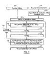
- FIG 1 shows an embodiment of fabricating the piezoelectric device, including the steps of making silicon (Si)/piezoelectric wafers, thinning the piezoelectric wafer, and depositing electrodes.
- Si wafer 103 and piezoelectric wafer 101 are firstly prepared.
- Si wafer preparation 101 involves detaining a silicon block of approximately 400 ⁇ m in thickness.
- Piezoelectric wafer preparation 100 involves obtaining a piezoelectric block of approximately 200 ⁇ m thick.
- an electrode is deposited thereon 105.
- the piezoelectric wafers can be made of crystal of the formula Pb (B I B II )O 3 -PbTiO 3 , where B I is Mg 2+ , Zn 2+ , Sc 3+ , and B II is Nb 5+ .
- Examples of piezoelectrics used in the wafers include Pb (Mg 1/3 Nb 2/3 )O 3 -PbTiO 3 (PMN-PT), Pb(Ni 1/3 Nb 2/3 )-PbTiO 3 (PNN-PT), Pb(Co 1/3 Nb 2/3 )O 3 , Pb(Zn 1/3 Nb 2/3 -PbTiO 3 (PZN-PT), (Bi 1/2 Na 1/2 )TiO 3 , and Pb(Sc 1/3 Nb 2/3 )O 3 -PbTiO 3 (PSN-PT).
- PMN-PT Pb(Mg 1/3 Nb 2/3 )O 3 -PbTiO 3
- PNN-PT Pb(Ni 1/3 Nb 2/3 )-PbTiO 3
- PZN-PT Pb(Zn 1/3 Nb 2/3 -PbTiO 3
- PZN-PT Pb(Sc 1/3 Nb 2/3 )O 3 -PbT
- the Si wafer and piezoelectrics wafer are then bonded 107 to form a piezoelectric-on-silicon wafer.
- the piezoelectric wafer Prior to bonding, the piezoelectric wafer is coated with a metallic layer to serve as a common bottom electrode 105.
- Application is preferably by AU/Cr Sputtering.
- the two wafers are bonded by means well-known in the art, including but not limited to eutectic bonding, soldering, or adhesive bonding.
- adhesive bonding an epoxy phenol adhesive is preferably spun-on the silicon wafer.
- An example of the epoxy phenol is M-Bond 610 by SPI Supplies Division Structure Probe, Inc.
- the two wafers are bonded at between 150°C to 200°C under pressure for approximately 1 to 3 hours.
- the piezoelectric wafer of the Si/piezoelectric wafer is then thinned 100.
- the piezoelectric layer is thinned using a 3-step process: wet chemical thinning, grinding, and polishing.
- Wet chemical thinning 109 occurs by applying a chemical formulation of 10 HC1:10H 2 O:1HF to the piezoelectric layer.
- the desired thinness should be from 5 to 50 ⁇ m.
- Grinding 111 is accomplished by methods well-known in the art, for example those disclosed in U.S.P. 6,742,914 , incorporated herein by reference.
- Polishing 113 can be applied by a variety of methods, such as dry tape polishing or wet polishing.
- the piezoelectric layer is then further thinned by wet chemical thinning. Electrodes are then deposited on the piezoelectric layer 109, and wet etching 111 is performed.
- FIG 2 is an embodiment of the piezoelectric-on-silicon wafer 200 made in accordance with the present invention.
- the wafer 200 includes the piezoelectric layer 201 made of a single crystal and having a thinness between 5-50 ⁇ m, an epoxy phenolic resin 203, and a silicon base 205.
- the piezoelectric-on-silicon wafer of the present invention is suitable for use on micro-electromechanical device, for example micro-cantilevers, acoustic sensors, ultrasonic transducer, resonators, and pressure sensors.
- the wafer can be used with, for example, opthalmological imaging equipment, determatogical imaging equipment, and intravascular imaging equipment.
- a 430 ⁇ m thick silicon wafer is bonded with a PMN-PT single crystal wafer of about 200 ⁇ m thick.
- spin-on M-Bond 610 adhesive SPI Supplies Division Structure Probe, Inc.
- the PMN-PT wafer is pre-coated with a metallic layer as a common bottom electrode.
- the two wafers are adhesively bonded at 175°C with light pressure for 2 hours.
- polishing and wet chemical thinning with a 10HCI:10H 2 O:1HF PMN-PT layers with thickness ranging from 5 to 50 ⁇ m, depending on processing parameters, can be achieved on the silicon substrate.
- top electrodes with various dimensions are deposited on the sample surface by using Au/Cr sputtering and photolithographic patterning.
- the sample is then connected through a probe station to a Agilent 4294 impedance analyzer and TF analyzer 2000 (for hysteresis loop measurement).
- the P-E hysteresis loop of the sample is measured and shown in FIG 3 .
- the remnant polarization P r ( ⁇ 30 ⁇ C/cm 2 ) of the 16-micron-thick PMN-PT thin layer is comparable to that of bulk 0.70PMN-0.30PT single crystal, whereas the coercive electric filed E c ( ⁇ 17.5 k V/cm) is much higher than that of bulk crystal ( ⁇ 2.4kV/cm) at room temperature.
- This 'piezoelectric hardening' may be attributed to the strong substrate constrain.
- the thickness dependence of coercive field E c of PMN-PT thich thin layers will be discussed elsewhere.
- the dielectric permittivity of ⁇ 33 T / ⁇ 0 (at 1 KHz) is 1416, measured according to the IEEE standards.
- a double-side polished silicon wafer (Si 3 N 4 /SiO 2 /Si/SiO 2 ) with 40-micron-thick PMN-PT single crystal layer is used for the fabrication.
- the Si 3 N 4 layer (200nm) is serving as the etching mask during the backside silicon
- KOH anisotropic etching of Si 3 N 4 and SiO 2 is done by RIE using SF 6 +Ar gas to open up wet etching windows (2 x 2 mm 2 ).
- Through-wafer silicon etching is then achieved by using KOH anisotropic etching until PMN-PT single crystal membranes (1.3 x 1.3 mm 2 ) are totally released.
- Cr/Au layers with 50nm/150nm thick are then sputtered and patterned on the PMN-PT membranes as top electrodes (0.7 x 0.7 mm 2 ) by using a double-side aligner (OAI).
- the top electrode defines the effective part of the transducer.
- the backside of the wafer is then coated with epoxy resin mixed with tungsten powder and hollow glass micro beads. After baking at 100°C in vacuum for 2 hours, the epoxy resin composite fills into the silicon cavities uniformly and is hardened to form a backing material whose acoustic impedance is about 6.23 Mrayls.
- the wafer is then diced into 5 x 5 mm 2 silicon dies. Each die carries a single element non-focused pMUT. Afterward, the silicon die is mounted on a small printed circuit board (PCB) and connected to a coaxial cable through wire bonding.
- PCB printed circuit board
- the fabricated prototype pMUT is poled under DC 140 volts for 15 minutes at room temperature.
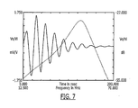
- the electric characteristics are measured by an Agilent 4294A impedance analyzer.
- , and phase angle are plotted versus frequency in FIG 5 .
- the resonant frequency (fr) and the anti-resonance frequency (fa) are approximately at 42 MHz and 50 MHz, respectively.
- the electromechanical coupling coefficient (kt) is calculated as 58.2%, which is nearly equal to the value of bulk 0.70PMN-0.30PT single crystal.
- the electrical impedance is about 50 ohm at resonance, matching perfectly with the input impedance of the oscilloscopes. Dielectric permittivity ⁇ 33 T / ⁇ 0 at 1 kHz is found to be about 1446 at room temperature.
- a pulser/receiver (Panametrics 5900PR) is used for ultrasonic pulse-echo measurement.
- a glass target is used as the reflector in a silicon oil tank at the standard measured distance.
- the received echo wave forms are displayed on an HP infinium oscilloscope (50 ohm coupling).
- a typical echo response of the pMUT is displayed in time domain and in frequency domain, as repectively shown in FIG. 6 (a) and (b) .
- the echo wave form exhibited a noticeable long ring down due to the acoustic impedance mismatch between the PMN-PT thick film (32 Mrayls) and the silicon oil (1.0 Mrayl).
- the bandwidth at -6dB was found to be about 25%. Further improvements shall include the deposition of an acoustic impedance matching layer on the front side of the wafer to increase the transducer sensitivity as well as to provide enough damping.
- KLM Krimholtz-Leedom-Matthae
Landscapes
- Engineering & Computer Science (AREA)
- Manufacturing & Machinery (AREA)
- Chemical & Material Sciences (AREA)
- Ceramic Engineering (AREA)
- Micromachines (AREA)
- Transducers For Ultrasonic Waves (AREA)
- Ultra Sonic Daignosis Equipment (AREA)
Applications Claiming Priority (1)
| Application Number | Priority Date | Filing Date | Title |
|---|---|---|---|
| US11/892,313 US8536665B2 (en) | 2007-08-22 | 2007-08-22 | Fabrication of piezoelectric single crystalline thin layer on silicon wafer |
Publications (2)
| Publication Number | Publication Date |
|---|---|
| EP2028703A2 true EP2028703A2 (de) | 2009-02-25 |
| EP2028703A3 EP2028703A3 (de) | 2010-09-01 |
Family
ID=40030275
Family Applications (1)
| Application Number | Title | Priority Date | Filing Date |
|---|---|---|---|
| EP08162225A Withdrawn EP2028703A3 (de) | 2007-08-22 | 2008-08-12 | Herstellung einer piezoelektrischen einkristallinen Dünnschicht auf einem Siliziumwafer |
Country Status (2)
| Country | Link |
|---|---|
| US (1) | US8536665B2 (de) |
| EP (1) | EP2028703A3 (de) |
Cited By (1)
| Publication number | Priority date | Publication date | Assignee | Title |
|---|---|---|---|---|
| WO2019122162A1 (en) * | 2017-12-21 | 2019-06-27 | RF360 Europe GmbH | Method of producing a thin film functional layer |
Families Citing this family (6)
| Publication number | Priority date | Publication date | Assignee | Title |
|---|---|---|---|---|
| US20050034087A1 (en) * | 2003-08-04 | 2005-02-10 | Hamlin Christopher L. | Method and apparatus for mapping platform-based design to multiple foundry processes |
| US8209857B2 (en) * | 2009-06-19 | 2012-07-03 | The Regents Of The University Of Michigan | Method of making a thin film device |
| US11706987B2 (en) | 2019-12-20 | 2023-07-18 | Globalfoundries Singapore Pte. Ltd. | Semiconductor device and method of forming a semiconductor device |
| KR102474555B1 (ko) * | 2020-07-02 | 2022-12-06 | (주)아이블포토닉스 | 압전 단결정 소자, 이를 이용한 멤스 디바이스 및 그 제조방법 |
| KR20260026197A (ko) * | 2024-08-19 | 2026-02-26 | 엘지이노텍 주식회사 | 변형 가능한 이미지 센서, 그 제조 방법 및 이를 포함한 카메라 모듈 |
| CN119387135B (zh) * | 2024-10-31 | 2026-01-30 | 重庆大学 | 一种新型宽频pMUT单元及其阵列 |
Citations (1)
| Publication number | Priority date | Publication date | Assignee | Title |
|---|---|---|---|---|
| US6746914B2 (en) | 2002-05-07 | 2004-06-08 | Chartered Semiconductor Manufacturing Ltd. | Metal sandwich structure for MIM capacitor onto dual damascene |
Family Cites Families (13)
| Publication number | Priority date | Publication date | Assignee | Title |
|---|---|---|---|---|
| JP3205976B2 (ja) * | 1992-09-14 | 2001-09-04 | 住友電気工業株式会社 | 表面弾性波素子 |
| US5371654A (en) * | 1992-10-19 | 1994-12-06 | International Business Machines Corporation | Three dimensional high performance interconnection package |
| US5838089A (en) * | 1997-02-18 | 1998-11-17 | Kobe Steel Usa Inc. | Acoustic wave devices on diamond with an interlayer |
| JP3880150B2 (ja) * | 1997-06-02 | 2007-02-14 | 松下電器産業株式会社 | 弾性表面波素子 |
| KR100316383B1 (ko) * | 1998-10-30 | 2002-02-19 | 윤덕용 | 모노리딕직접회로위에박막또는후막단결정압전소자를집적한단일칩라디오구조및그제조방법 |
| JP3714082B2 (ja) * | 2000-01-13 | 2005-11-09 | 株式会社村田製作所 | ランガサイト系単結晶基板の製造方法、ランガサイト系単結晶基板および圧電デバイス |
| US6814130B2 (en) * | 2000-10-13 | 2004-11-09 | Chien-Min Sung | Methods of making diamond tools using reverse casting of chemical vapor deposition |
| DE10112433A1 (de) * | 2001-03-15 | 2002-10-02 | Bosch Gmbh Robert | Messanordnung für eine Viskositätsmessung von Flüssigkeiten |
| WO2002082644A1 (fr) * | 2001-03-30 | 2002-10-17 | Mitsubishi Denki Kabushiki Kaisha | Dispositif d'onde acoustique et procede de fabrication correspondant |
| US7105980B2 (en) * | 2002-07-03 | 2006-09-12 | Sawtek, Inc. | Saw filter device and method employing normal temperature bonding for producing desirable filter production and performance characteristics |
| US8326388B2 (en) * | 2002-10-31 | 2012-12-04 | Toshiba Medical Systems Corporation | Method and apparatus for non-invasive measurement of living body characteristics by photoacoustics |
| US7089635B2 (en) * | 2003-02-25 | 2006-08-15 | Palo Alto Research Center, Incorporated | Methods to make piezoelectric ceramic thick film arrays and elements |
| DE102004045181B4 (de) * | 2004-09-17 | 2016-02-04 | Epcos Ag | SAW-Bauelement mit reduziertem Temperaturgang und Verfahren zur Herstellung |
-
2007
- 2007-08-22 US US11/892,313 patent/US8536665B2/en active Active
-
2008
- 2008-08-12 EP EP08162225A patent/EP2028703A3/de not_active Withdrawn
Patent Citations (1)
| Publication number | Priority date | Publication date | Assignee | Title |
|---|---|---|---|---|
| US6746914B2 (en) | 2002-05-07 | 2004-06-08 | Chartered Semiconductor Manufacturing Ltd. | Metal sandwich structure for MIM capacitor onto dual damascene |
Cited By (1)
| Publication number | Priority date | Publication date | Assignee | Title |
|---|---|---|---|---|
| WO2019122162A1 (en) * | 2017-12-21 | 2019-06-27 | RF360 Europe GmbH | Method of producing a thin film functional layer |
Also Published As
| Publication number | Publication date |
|---|---|
| EP2028703A3 (de) | 2010-09-01 |
| US20090050987A1 (en) | 2009-02-26 |
| US8536665B2 (en) | 2013-09-17 |
Similar Documents
| Publication | Publication Date | Title |
|---|---|---|
| EP2028703A2 (de) | Herstellung einer piezoelektrischen einkristallinen Dünnschicht auf einem Siliziumwafer | |
| JP7517840B2 (ja) | 転写圧電又は強誘電体層から微小電気機械システムを製造するプロセス | |
| WO2007134051A2 (en) | High frequency ultrasound transducers | |
| Yuan et al. | 5I-1 Microfabrication of piezoelectric composite ultrasound transducers (PC-MUT) | |
| Lukacs et al. | Single element high frequency (< 50 MHz) PZT sol gel composite ultrasound transducers | |
| EP1384525A2 (de) | Piezoelektrischer Komposit-Wandler und Verfahren zur dessen Herstellung | |
| Wang et al. | Scandium doped aluminum nitride based piezoelectric micromachined ultrasound transducers | |
| Zhao et al. | Broadband and high-pressure output pMUT array based on lead-free KNN thin film | |
| Jiang et al. | Micromachined PMN-PT single crystal composite transducers--15–75 MHz PC-MUT | |
| Zhou et al. | Micro-machined high-frequency (80 MHz) PZT thick film linear arrays | |
| KR20050004815A (ko) | 컴포지트 압전체 | |
| WO2003042687A1 (en) | Ultrasonic probe | |
| Sleva et al. | A micromachined poly (vinylidene fluoride-trifluoroethylene) transducer for pulse-echo ultrasound applications | |
| KR100671419B1 (ko) | 고주파 초음파 센서용 음향 정합층 및 그를 이용한 초음파센서의 제조 방법 | |
| Peng et al. | PMN-PT single crystal thick films on silicon substrate for high-frequency micromachined ultrasonic transducers | |
| Pedersen et al. | Fabrication of high-frequency pMUT arrays on silicon substrates | |
| US12337347B2 (en) | Lithium-based piezoelectric micromachined ultrasonic transducer | |
| JP2013026682A (ja) | 医用複合単結晶圧電振動子、医用超音波プローブ、医用複合単結晶圧電振動子製造方法および医用超音波プローブ製造方法 | |
| Gentry et al. | Thick film sol gel PZT transducer using dip coating | |
| Peng et al. | PMN-PT single crystal thick films on silicon substrate for high-frequency micromachined ultrasonic transducers | |
| Lai et al. | Universal Concept for Fabricating Low Residual Stress PZT Film-Based PMUT on Silicon Wafer Using Bottom-Up Method | |
| JP2003174698A (ja) | 複合圧電体およびその製造方法 | |
| Yan et al. | Piezoelectric micromechanical disk resonators towards UHF band | |
| JP2004120320A (ja) | 超音波トランスデューサアレイ及びその製造方法 | |
| Zhou et al. | High frequency piezoelectric micromachined ultrasonic transducers for imaging applications |
Legal Events
| Date | Code | Title | Description |
|---|---|---|---|
| PUAI | Public reference made under article 153(3) epc to a published international application that has entered the european phase |
Free format text: ORIGINAL CODE: 0009012 |
|
| AK | Designated contracting states |
Kind code of ref document: A2 Designated state(s): AT BE BG CH CY CZ DE DK EE ES FI FR GB GR HR HU IE IS IT LI LT LU LV MC MT NL NO PL PT RO SE SI SK TR |
|
| AX | Request for extension of the european patent |
Extension state: AL BA MK RS |
|
| PUAL | Search report despatched |
Free format text: ORIGINAL CODE: 0009013 |
|
| AK | Designated contracting states |
Kind code of ref document: A3 Designated state(s): AT BE BG CH CY CZ DE DK EE ES FI FR GB GR HR HU IE IS IT LI LT LU LV MC MT NL NO PL PT RO SE SI SK TR |
|
| AX | Request for extension of the european patent |
Extension state: AL BA MK RS |
|
| RIC1 | Information provided on ipc code assigned before grant |
Ipc: B06B 1/06 20060101ALI20100723BHEP Ipc: B81C 1/00 20060101ALI20100723BHEP Ipc: H01L 41/22 20060101AFI20081204BHEP |
|
| AKY | No designation fees paid | ||
| STAA | Information on the status of an ep patent application or granted ep patent |
Free format text: STATUS: THE APPLICATION IS DEEMED TO BE WITHDRAWN |
|
| 18D | Application deemed to be withdrawn |
Effective date: 20110302 |