EP2028691A2 - Sacrificial structures for crack propagation confinement in a substrate comprising a plurality of ICs - Google Patents
Sacrificial structures for crack propagation confinement in a substrate comprising a plurality of ICs Download PDFInfo
- Publication number
- EP2028691A2 EP2028691A2 EP08014445A EP08014445A EP2028691A2 EP 2028691 A2 EP2028691 A2 EP 2028691A2 EP 08014445 A EP08014445 A EP 08014445A EP 08014445 A EP08014445 A EP 08014445A EP 2028691 A2 EP2028691 A2 EP 2028691A2
- Authority
- EP
- European Patent Office
- Prior art keywords
- unit
- functional area
- substrate
- vias
- preventive structure
- Prior art date
- Legal status (The legal status is an assumption and is not a legal conclusion. Google has not performed a legal analysis and makes no representation as to the accuracy of the status listed.)
- Withdrawn
Links
Images





Classifications
-
- H—ELECTRICITY
- H10—SEMICONDUCTOR DEVICES; ELECTRIC SOLID-STATE DEVICES NOT OTHERWISE PROVIDED FOR
- H10W—GENERIC PACKAGES, INTERCONNECTIONS, CONNECTORS OR OTHER CONSTRUCTIONAL DETAILS OF DEVICES COVERED BY CLASS H10
- H10W74/00—Encapsulations, e.g. protective coatings
-
- H—ELECTRICITY
- H10—SEMICONDUCTOR DEVICES; ELECTRIC SOLID-STATE DEVICES NOT OTHERWISE PROVIDED FOR
- H10P—GENERIC PROCESSES OR APPARATUS FOR THE MANUFACTURE OR TREATMENT OF DEVICES COVERED BY CLASS H10
- H10P54/00—Cutting or separating of wafers, substrates or parts of devices
-
- H—ELECTRICITY
- H05—ELECTRIC TECHNIQUES NOT OTHERWISE PROVIDED FOR
- H05K—PRINTED CIRCUITS; CASINGS OR CONSTRUCTIONAL DETAILS OF ELECTRIC APPARATUS; MANUFACTURE OF ASSEMBLAGES OF ELECTRICAL COMPONENTS
- H05K3/00—Apparatus or processes for manufacturing printed circuits
- H05K3/0011—Working of insulating substrates or insulating layers
- H05K3/0044—Mechanical working of the substrate, e.g. drilling or punching
- H05K3/0052—Depaneling, i.e. dividing a panel into circuit boards; Working of the edges of circuit boards
-
- H—ELECTRICITY
- H10—SEMICONDUCTOR DEVICES; ELECTRIC SOLID-STATE DEVICES NOT OTHERWISE PROVIDED FOR
- H10W—GENERIC PACKAGES, INTERCONNECTIONS, CONNECTORS OR OTHER CONSTRUCTIONAL DETAILS OF DEVICES COVERED BY CLASS H10
- H10W42/00—Arrangements for protection of devices
-
- H—ELECTRICITY
- H10—SEMICONDUCTOR DEVICES; ELECTRIC SOLID-STATE DEVICES NOT OTHERWISE PROVIDED FOR
- H10W—GENERIC PACKAGES, INTERCONNECTIONS, CONNECTORS OR OTHER CONSTRUCTIONAL DETAILS OF DEVICES COVERED BY CLASS H10
- H10W42/00—Arrangements for protection of devices
- H10W42/121—Arrangements for protection of devices protecting against mechanical damage
-
- H—ELECTRICITY
- H10—SEMICONDUCTOR DEVICES; ELECTRIC SOLID-STATE DEVICES NOT OTHERWISE PROVIDED FOR
- H10W—GENERIC PACKAGES, INTERCONNECTIONS, CONNECTORS OR OTHER CONSTRUCTIONAL DETAILS OF DEVICES COVERED BY CLASS H10
- H10W72/00—Interconnections or connectors in packages
-
- H—ELECTRICITY
- H05—ELECTRIC TECHNIQUES NOT OTHERWISE PROVIDED FOR
- H05K—PRINTED CIRCUITS; CASINGS OR CONSTRUCTIONAL DETAILS OF ELECTRIC APPARATUS; MANUFACTURE OF ASSEMBLAGES OF ELECTRICAL COMPONENTS
- H05K2201/00—Indexing scheme relating to printed circuits covered by H05K1/00
- H05K2201/09—Shape and layout
- H05K2201/09009—Substrate related
- H05K2201/09063—Holes or slots in insulating substrate not used for electrical connections
-
- H—ELECTRICITY
- H05—ELECTRIC TECHNIQUES NOT OTHERWISE PROVIDED FOR
- H05K—PRINTED CIRCUITS; CASINGS OR CONSTRUCTIONAL DETAILS OF ELECTRIC APPARATUS; MANUFACTURE OF ASSEMBLAGES OF ELECTRICAL COMPONENTS
- H05K2201/00—Indexing scheme relating to printed circuits covered by H05K1/00
- H05K2201/09—Shape and layout
- H05K2201/09209—Shape and layout details of conductors
- H05K2201/09654—Shape and layout details of conductors covering at least two types of conductors provided for in H05K2201/09218 - H05K2201/095
- H05K2201/09681—Mesh conductors, e.g. as a ground plane
-
- H—ELECTRICITY
- H05—ELECTRIC TECHNIQUES NOT OTHERWISE PROVIDED FOR
- H05K—PRINTED CIRCUITS; CASINGS OR CONSTRUCTIONAL DETAILS OF ELECTRIC APPARATUS; MANUFACTURE OF ASSEMBLAGES OF ELECTRICAL COMPONENTS
- H05K2201/00—Indexing scheme relating to printed circuits covered by H05K1/00
- H05K2201/09—Shape and layout
- H05K2201/09209—Shape and layout details of conductors
- H05K2201/09654—Shape and layout details of conductors covering at least two types of conductors provided for in H05K2201/09218 - H05K2201/095
- H05K2201/09781—Dummy conductors, i.e. not used for normal transport of current; Dummy electrodes of components
Definitions
- the present invention relates to IC packaging, and more particularly, to preventing damage from crack propagation.
- IC packages In forming integrated circuit (IC) packages, multiple units (e.g., substrates, IC die, etc.) are often formed simultaneously. Each of these units is then separated in a singulation process. However, units are often damaged in such a singulation process when stress is exerted on areas of the unit. In particular, cracks resulting from the exerted stress can render circuit traces, circuit connectors, electrical devices, IC components, and other features non-operational.
- IC integrated circuit
- a unit of a collection of units includes a functional area and a preventive structure configured to prevent cracks from propagating into the functional area.
- a unit of a collection of units comprises:
- FIG. 1 shows a strip of units.
- FIG. 2 shows a cross-sectional view of an exemplary unit.
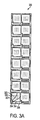
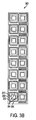
- FIGS. 3A and 3B shows top and bottom views, respectively, of a strip of units, according to an embodiment of the present invention.
- FIGS. 4A-4C show substrates including preventive structures, according to an embodiment of the present invention.
- FIGS. 5A-5C shows substrates that include a plurality of vias, according to an embodiment of the present invention.
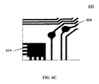
- FIGS. 6A-6C shows substrates that include exposed regions, according to an embodiment of the present invention.
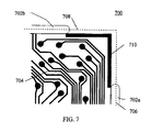
- FIGS. 7 shows a substrate that includes a solder mask slot, according to an embodiment of the present invention.
- FIG. 8A and 8B show aspects of a wafer, according to an embodiment of the present invention.
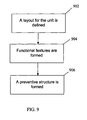
- FIG. 9 shows a flowchart providing example steps for forming a unit, according to an embodiment of the present invention.
- FIG. 1 shows a strip of units 100 that includes a plurality of units 102.
- Plurality of units 102 may include substrates, integrated circuit (IC) packages, and/or other types of electrical devices.
- strip 100 may be a wafer or a portion of a wafer than includes a collection of IC semiconductor die.
- unit 102a of plurality of units 102 In order for a unit 102a of plurality of units 102 to be used for its intended purpose, it must be separated from strip 100 in a singulation process.
- unit 102a may be a substrate to be used in a plastic ball grid array (PBGA) package or other circuit package.
- PBGA plastic ball grid array
- Unit 102a may be singulated in a variety of ways.
- methods for unit singulation may include sawing, punching, abrasive particle cutting, and focused laser beam ablation cutting. All of the above mentioned methods involve stress being applied to unit 102a and/or adjacent units 102b and 102c.
- stress from a singulation process is present along boundaries 104 and 106.
- unit 102a may be singulated by sawing along boundaries 104 and 106 or applying a force on the top of unit 102a in a punching action.
- unit 102a has a functional area 103.
- Functional area 103 may contain circuit traces, connectors, circuit elements, IC features, and/or other features that are important to the operation of unit 102a. Thus, functional area 103 should be protected from cracks.
- unit 102a As unit 102a is singulated, areas of unit 102a, as well as other areas of strip 100, experience stress. This stress often leads to a release of energy in the form of a crack. As cracks propagate, they may cause damage to areas within functional area 103 and render unit 102a damaged or non-functional.
- boundaries 104 and 106 may be scored. In such an embodiment, areas immediately surrounding boundaries 104 and 106 are weakened to prepare for a singulation process. Scoring may involve removing material and/or partially cutting along boundary 104 and/or boundary 106. Additionally or alternatively, boundaries 104 and 106 may be scored with a laser beam. In such an embodiment boundaries 104 and 106 are ablated or melted by the laser beam and then re-solidify into a more planar profile, thereby reducing areas of stress concentration along boundaries 104 and 106 that contribute to cracking and chipping during singulation.
- FIG. 2 shows a cross-sectional view of an exemplary unit 200.
- Unit 200 is presented by way of example is not meant to limit the definition of a unit, as described herein.
- Unit 200 may be included in a strip of units similar to strip 100, as described with reference to FIG. 1 .
- Unit 200 includes a signal layer 202 and a power layer 204 that sandwich a ground plane 206.
- Signal layer 202 may be patterned to form electrical traces and connectors.
- Ground plane 206 is insulated from signal layer 202 by a prepreg layer 208.
- Prepreg layer 208 comprises a fiber or an epoxy material with a high dielectric constant and toughness.
- Ground plane 206 is insulated from power layer 204 by a layer of BT-epoxy or FR-4 210 .
- Layer 210 may also be formed out of other suitable printed circuit board (PCB) composites.
- PCB composites exhibit constant, high dielectric constants, and are nearly lossless, even at higher frequencies.
- IC package stack signal layer 202 is sealed and protected from exposure by solder mask 212.
- Solder mask 212 is etched to allow access to functional elements (e.g., circuit traces, connectors, etc.) of signal layer 202.
- a crack typically will propagate along the weakest segment under stress. Without any structure to prevent or mitigate crack propagation, cracks may propagate into functional areas of a unit and potentially cut through electrical traces, sever vias, or crack, chip, peel, or delaminate substrate layers. Damage to the unit incurred during a singulation process can be reduced using the techniques and embodiments presented herein.
- Preventive structures may be formed on a unit to prevent cracks from propagating into functional areas of the unit.
- the preventive structures may be formed in areas of the unit that will be exposed to stress as the unit is singulated.
- preventive structures areas of a unit may be strengthened. Strengthened portions absorb and/or reflect cracking energy so that cracks will not propagate into functional areas of the unit. Alternatively, areas of the unit may be weakened. As described above, cracks tend to propagate along weak areas. By weakening an area away from the functional areas of the unit, cracks may be confined to such an area and avoid the functional areas. Preventive structures may include structures that both weaken given areas of a unit and strengthen other areas of a unit.
- FIGS. 3A and 3B show top and bottom views of a strip of units 300, respectively, according to an embodiment of the present invention.
- Strip 300 includes a unit 302.
- Unit 302 includes a functional area 303 and slots 304 and 306. Similar to functional area 103 described reference to FIG. 1 above, functional area 303 may include functional features and elements of unit 302.
- functional area 303 may include an area for an IC die or contact pads so that solder balls, pins, etc. may be attached.
- Slots 304 and 306 are preventive structures that are configured to prevent cracks from propagating into functional area 303.
- slots 304 and 306 weaken areas of unit 302 that will experience stress during a singulation process (e.g., along the boundaries of unit 302 with neighboring units). Cracks that may develop as a result of a singulation process may be confined to slots 304 and 306, and thus be prevented from propagating into functional area 303.
- Slots 304 generally have a larger width than slot 306 because slot 306 is located along an edge portion of strip 300 (i.e., does not border any other unit) in which space is limited. In alternate embodiments, slot 306 may have a width substantially similar to or larger than slots 304.
- Slots 304 and 306 may be formed partially or completely through unit 302. In other words, slots 304 and 306 may be areas of unit 302 where material is completely removed (i.e., a hole) or where material is partially removed.
- FIG. 3A also shows unit 302 as having a mold top 308.
- mold top 308 is configured to shape the mold or encapsulation material that will encapsulate a package (e.g., a PBGA package) that includes unit 302.
- a package e.g., a PBGA package
- slots 304 and 306 do not extend all the way along boundaries that separate units of strip 300. Slots that extend all way along boundaries 304 and 306 may reduce the structural integrity of strip 300.
- structures are described that provide additional ways to prevent cracks from propagating into functional areas. These structures may or may not be used along with slots, as described above.
- FIGS. 4A-4C show substrates 400, 420, and 440, respectively, according to embodiments of the present invention.
- each of substrates 400, 420, and 440 are units in a strip of units similar to strip of units 100 described with reference to FIG. 1 .
- Each of substrates 400, 420, and 440 includes slots 402a and 402b and a functional areas 404. Slots 402a and 402b are formed along boundaries 406 and 408, respectively, that separate the substrates from other units. Slots 402a and 402b may be generally similar to slot 304 and/or slots 306 as described with reference to FIG. 3 , above.
- Each of substrates 400, 420, and 440 include a pattern that is configured to prevent cracks from propagating into functional areas 404.
- FIGS. 4A-4C are shown to be formed on substrate, those skilled in the relevant arts would appreciate that the patterns shown may also be applied to other types of units.
- a mesh 410 is formed on substrate 400 to strengthen substrate 410 along boundaries 406 and 408.
- Mesh 410 serves to confine cracks to areas within mesh 410 and to protect functional areas 404. For example, if a crack occurs as a result of stress along boundary 406, that crack may be confined by slots 402a and 402b and/or mesh 410, thereby protecting functional features 404.
- mesh 410 may be configured to absorb cracking energy, so as to prevent cracks from forming and/or propagating.
- lines 412 formed on substrate 420 and planes 414 formed on substrate 440 are formed to prevent cracks from propagating into functional areas 404.
- lines 412 include a plurality of horizontal and vertical lines formed on substrate 420.
- planes 414 include a plurality of planes formed on substrate 440.
- Mesh 410 and planes 414 are shown to be similar in FIGS. 4A and 4C respectively. However, mesh 410 may be made up lines that are broken at intersections while planes 414 may be made up of lines that are continuous at intersections.
- mesh 410, lines 412, and planes 414 may be formed on two or more layers of the substrate.
- patterns formed on different layers may be coupled together through the use of vias. Alternatively, the structures may remain isolated.
- a four layer substrate may have a mesh formed on a first layer, lines formed on a second layer and a third layer, and planes formed on a fourth layer.
- mesh 410, lines 412, and planes 414 may be formed out of a metallic material (e.g., copper, copper alloy, gold, etc.).
- functional areas 404 include circuit traces or other similar features
- mesh 410, lines 412, and/or planes 414 may be formed out of the same material and have line widths comparable to features of functional area 404.
- mesh 410, lines 412, and/or planes 414 may be may be included in the layout of the respective substrate and be patterned onto a substrate during the same fabrication process in which features of functional area 404 are formed on the substrate.
- FIG. 5A shows a substrate 500 including preventive structures, according to an embodiment of the present invention.
- Substrate 500 includes slots 502a and 502b, a functional area 504, and a plurality of vias 510.
- Slots 502a and 502b are generally similar to slots 402a and 402b, described with reference to FIGS. 4A-4C above.
- functional area 504 may include circuit traces, circuit connectors, electrical components, etc.
- Substrate 500 includes a plurality of vias 510 formed along boundaries 506 and 508. Similar to boundaries 406 and 408 described with reference to FIGS. 4A-4C , boundaries 506 and 508 may separate substrate 500 from other units of a strip or collection of units and may be areas where stress from a singulation process is felt. As shown in FIG. 5 , plurality of vias 510 effectively forms a fence that protects functional area 504 from cracks. In an embodiment, plurality of vias 510 may absorb and/or reflect cracking energy so as to prevent cracks from propagating into functional areas 504.
- substrate 500 may include multiple layers.
- vias of plurality of vias 510 may extend to some or all layers of the substrate.
- Vias of plurality of vias 510 may be plated and/or filled and may be metallic.
- vias of plurality of vias 510 may include copper, a copper alloy, aluminum, etc.
- functional area 504 includes a via.
- vias of the plurality of vias 510 may be substantially similar, in terms of composition, size, etc., to the via of functional area 504.
- vias of plurality of vias 510 may be included in the layout of substrate 500 and may be and fabricated in the same process in which features of functional area 504 are fabricated.
- plurality of vias 510 is formed as a combination of two lines of vias.
- plurality of vias 510 may be arranged in other shapes without departing from the scope and spirit of the present invention.
- FIGS. 5B and 5C show other implementations of a preventive structure that includes a plurality of vias, according to embodiments of the present invention.
- FIG. 5B shows a substrate 520 that that is generally similar to substrate 500. However, substrate 520 additionally includes a solder mask 522 and a plurality of vias 524. As shown in FIG. 5B , vias of plurality of vias 524 do not penetrate solder mask 522. In an alternate embodiment, one or more vias of plurality of vias 524 may partially or completely penetrate solder mask 522. In an embodiment, vias of plurality of vias 524 are formed along an edge of substrate 520 (e.g., a boundary between substrate 520 and another unit in a strip or collection of units). Similar to plurality of vias 510 described with reference to FIG. 5A , plurality of vias 524 are configured to absorb and or reflect cracking energy so cracks do not propagate into functional areas.
- FIG. 5C shows a substrate 540 that includes a plurality of vias 542, a plurality of slabs 544, a metal pad 546, a passivation 548, and a bond opening 550.
- substrate 540 includes a mesh formed by plurality of vias 542 and plurality of slabs 544.
- slabs of plurality of slabs 544 may be made up of a metallic material (e.g., copper, copper alloy, aluminum) and may be similar in composition to plurality of vias 542.
- plurality of vias 542 and plurality of slabs 544 form mesh preventive structure that absorbs and/or reflects cracking energy.
- the mesh shown in FIG. 5C is different from mesh 410 described reference to FIG.
- the mesh of plurality of vias 542 and plurality of slabs 544 is a three dimensional structure that is formed through portions of substrate 540.
- Passivation 548 may be configured to isolate elements of substrate 540 (e.g., metal pad 546) from other elements of substrate 540.
- FIGS. 6A-6C show substrates 600, 620, and 630 that include exposed plated regions 606, 610, and 614, respectively, according to embodiments of the present invention.
- Substrate 600 includes a functional area 604 generally similar to functional area 404 described with reference to FIG. 4 , above, and exposed region 606 formed along an edge portion of substrate 600.
- substrate 600 is covered with a solder mask.
- the solder mask may be used to identify regions of substrate 600 where solder should be deposited.
- the solder mask is substantially rigid.
- cracks resulting from stress exerted in a singulation process may tend to peel or tear the solder mask. Such peeling or tearing may inflict damage to features of functional area 604.
- exposed region 606 may also be configured to prevent tears or peels from propagating into functional area 604.
- Exposed plated regions 606, 610, and 614 may be areas where the solder mask is not present. Instead, exposed plated regions 606, 610, and 614 may be areas where substrate 600 is plated with a material.
- Exposed plated areas 606, 610, and 614 may be formed out of a metallic material, such as copper, a copper alloy, aluminum, etc. In another embodiment, exposed regions may be plated with a corrosive resistant material such as gold, silver, etc.
- exposed region 604 is formed in a substantially triangular shape in a corner portion of substrate 600.
- an exposed plated region may be formed in other shapes.
- FIGS. 6B and 6C show exposed plated regions 610 and 614 formed along edge portions 608 and 610, respectively.
- Exposed plated region 610 is formed in a substantially rectangular form and has a notch formed therein.
- Exposed plated region 614 is includes a substantially rectangular portion that a plurality of lines.
- exposed plated regions may have other shapes without departing from the scope and spirit of the present invention.
- exposed plated regions may also be combined with slots, as described above, to prevent damage to features of functional area 604.
- FIG. 7 shows a substrate 700 that includes slots 702a and 702b, a functional area 704, and a solder mask slot 710, according to embodiment of the present invention.
- slots 702a and 702b, formed along boundaries 706 and 708, respectively, are substantially similar to slots 402a and 402b, respectively, described with reference to FIGS. 4A-4C above.
- Functional area 704 may include features similar to functional area 404, described with reference to FIG. 4 , above.
- slot 710 is configured to prevent cracks from propagating into functional area 704.
- solder mask slot 710 may only be formed in a solder mask of substrate 700. In such an embodiment, solder mask slot 710 may also be configured to prevent peeling and/or tearing of the solder mask.
- Solder mask slot 710 weakens the solder mask in areas that may be exposed to stress during a singulation process. In such a way, a cracking energy may be confined by solder mask slot 710 and, thus prevented from causes tearing or peeling of the solder mask in functional areas 704. Upon reaching solder mask slot 710 a peel or crack will tend to move along solder mask slot 710 since it offers less resistance than the solder mask in other areas. Thus, the peel or crack would be confined in an area away from functional area 704.
- solder mask slot 710 is formed along edge portions of substrate 700.
- solder mask slot 710 may be formed in different shapes without departing from the scope and spirit of the present invention.
- FIGS. 8A and 8B show top and cross-sectional views of aspects of a wafer, according to an embodiment of the present invention.
- an IC die 800 which includes a functional area 804, is at least partially surrounded by a seal ring 802.
- Functional area 804 may include integrated circuit transistors, resistors, and/or or other types of electrical or logic components that may be included in an IC die or other semiconductor device.
- Seal ring 802 is configured to prevent cracks from propagating into functional area 804.
- FIG. 8B shows a cross-sectional view of seal ring 802 of IC die 800.
- Seal ring 802 includes line vias 804 and square vias 806.
- Line vias 804 and square vias 806 is configured to absorb and/or reflect crack energy so that cracks do not propagate into functional area 804.
- seal ring 802 also includes slabs 808.
- Slabs 808 may be formed horizontally (whereas vias are formed vertically) to create a three dimensional mesh. Slabs 808 may be similar to line vias and/or square vias 806 in composition.
- seal ring 802 may include any other combination of line vias 804, square vias 806, and slabs 808.
- FIG. 9 shows flowchart 900 providing example steps for forming a unit, according to an embodiment of the present invention.
- Other structural and operational embodiments will be apparent to persons skilled in the relevant art(s) based on the following discussion.
- the steps shown in FIG. 9 do not necessarily have to occur in the order shown.
- the steps of FIG. 9 are described in detail below.
- Flowchart 900 begins in step 902.
- a layout for the unit is defined.
- the unit is a substrate
- a layout including circuit traces and circuit connectors may be defined.
- IC elements such as resistors and transistors may be defined.
- a layout for a preventive structure that is configured prevent cracks from propagating into functional areas of the unit may also be defined along with the layout for the functional features.
- step 902 may include laying out functional features and laying out the preventive structure.
- step 904 functional features are formed.
- functional features such as circuit traces, IC elements, or other features may be formed in functional areas of the unit.
- preventive structures are formed. For example, one or more of slots, lines, meshes, planes, seal rings or other structures, as described above, may be formed on the unit.
- steps 904 and 906 may be completed during the same step of a fabrication process. Fabricating the functional features and the preventive structures during the same step may reduce the cost associated with forming the preventive structures.
Landscapes
- Engineering & Computer Science (AREA)
- Manufacturing & Machinery (AREA)
- Microelectronics & Electronic Packaging (AREA)
- Internal Circuitry In Semiconductor Integrated Circuit Devices (AREA)
- Design And Manufacture Of Integrated Circuits (AREA)
- Structure Of Printed Boards (AREA)
- Led Device Packages (AREA)
Abstract
Description
- This application claims the benefit of
U.S. Provisional Appl. No. 60/935,606, filed August 21, 2007 - The present invention relates to IC packaging, and more particularly, to preventing damage from crack propagation.
- In forming integrated circuit (IC) packages, multiple units (e.g., substrates, IC die, etc.) are often formed simultaneously. Each of these units is then separated in a singulation process. However, units are often damaged in such a singulation process when stress is exerted on areas of the unit. In particular, cracks resulting from the exerted stress can render circuit traces, circuit connectors, electrical devices, IC components, and other features non-operational.
- As the demand for increased throughput continues to rise, preventing cracks from damaging one or more units of a strip becomes important. Furthermore, as units become smaller, collections of units tend to become increasingly dense so that the likelihood that a crack will seriously damage one or more units increases.
- Thus, what is needed is methods and systems for preventing damage from crack propagation.
- Systems and methods for preventing damage to a unit with preventive structures are presented. In an embodiment, a unit of a collection of units includes a functional area and a preventive structure configured to prevent cracks from propagating into the functional area.
According to an aspect, a unit of a collection of units comprises: - a functional area; and
- a preventive structure configured to prevent cracks from propagating into the functional area.
- forming a functional area; and
- forming a preventive structure configured to prevent cracks from propagating into the functional area.
- laying out the functional area; and
- laying out the preventive structure.
- forming a pattern selected from the group consisting of a mesh, a plurality of lines, and a plurality of planes on a surface of the unit.
Advantageously, forming the preventive structure comprises:- forming a via.
- forming a plated region on a surface of the unit.
- forming a slot in a solder mask of the unit.
Advantageously, forming the preventive structure comprises:- forming a slot in the unit.
- Further embodiments, features, and advantages of the invention, as well as the structure and operation of the various embodiments of the invention are described in detail below with reference to accompanying drawings.
- The present invention is described with reference to the accompanying drawings. In the drawings, like reference numbers indicate identical or functionally similar elements. The drawing in which an element first appears is indicated by the left-most digit in the corresponding reference number.
-
FIG. 1 shows a strip of units. -
FIG. 2 shows a cross-sectional view of an exemplary unit. -
FIGS. 3A and3B shows top and bottom views, respectively, of a strip of units, according to an embodiment of the present invention. -
FIGS. 4A-4C show substrates including preventive structures, according to an embodiment of the present invention. -
FIGS. 5A-5C shows substrates that include a plurality of vias, according to an embodiment of the present invention. -
FIGS. 6A-6C shows substrates that include exposed regions, according to an embodiment of the present invention. -
FIGS. 7 shows a substrate that includes a solder mask slot, according to an embodiment of the present invention. -
FIG. 8A and 8B show aspects of a wafer, according to an embodiment of the present invention. -
FIG. 9 shows a flowchart providing example steps for forming a unit, according to an embodiment of the present invention. - The present invention will now be described with reference to the accompanying drawings. In the drawings, like reference numbers indicate identical or functionally similar elements. Additionally, the left-most digit(s) of a reference number identifies the drawing in which the reference number first appears.
- While the present invention is described herein with reference to illustrative embodiments for particular applications, it should be understood that the invention is not limited thereto. Those skilled in the art with access to the teachings provided herein will recognize additional modifications, applications, and embodiments within the scope thereof and additional fields in which the invention would be of significant utility.
-
FIG. 1 shows a strip ofunits 100 that includes a plurality ofunits 102. Plurality ofunits 102 may include substrates, integrated circuit (IC) packages, and/or other types of electrical devices. In other embodiments,strip 100 may be a wafer or a portion of a wafer than includes a collection of IC semiconductor die. In order for aunit 102a of plurality ofunits 102 to be used for its intended purpose, it must be separated fromstrip 100 in a singulation process. For example,unit 102a may be a substrate to be used in a plastic ball grid array (PBGA) package or other circuit package. Onceunit 102a is separated fromstrip 100,unit 102a may be combined with an IC die, solder balls, and other appropriate aspects to form the desired PBGA package. -
Unit 102a may be singulated in a variety of ways. For example, methods for unit singulation may include sawing, punching, abrasive particle cutting, and focused laser beam ablation cutting. All of the above mentioned methods involve stress being applied tounit 102a and/oradjacent units boundaries unit 102a may be singulated by sawing alongboundaries unit 102a in a punching action. - As shown in
FIG. 1 ,unit 102a has afunctional area 103.Functional area 103 may contain circuit traces, connectors, circuit elements, IC features, and/or other features that are important to the operation ofunit 102a. Thus,functional area 103 should be protected from cracks. - As
unit 102a is singulated, areas ofunit 102a, as well as other areas ofstrip 100, experience stress. This stress often leads to a release of energy in the form of a crack. As cracks propagate, they may cause damage to areas withinfunctional area 103 and renderunit 102a damaged or non-functional. - To reduce the damage caused by cracks, a number of approaches have been developed. For example,
boundaries boundaries boundary 104 and/orboundary 106. Additionally or alternatively,boundaries embodiment boundaries boundaries -
FIG. 2 shows a cross-sectional view of anexemplary unit 200.Unit 200 is presented by way of example is not meant to limit the definition of a unit, as described herein.Unit 200 may be included in a strip of units similar tostrip 100, as described with reference toFIG. 1 .Unit 200 includes asignal layer 202 and apower layer 204 that sandwich aground plane 206.Signal layer 202 may be patterned to form electrical traces and connectors.Ground plane 206 is insulated fromsignal layer 202 by aprepreg layer 208.Prepreg layer 208 comprises a fiber or an epoxy material with a high dielectric constant and toughness.Ground plane 206 is insulated frompower layer 204 by a layer of BT-epoxy orFR-4 210 Layer 210 may also be formed out of other suitable printed circuit board (PCB) composites. PCB composites exhibit constant, high dielectric constants, and are nearly lossless, even at higher frequencies. - IC package
stack signal layer 202 is sealed and protected from exposure bysolder mask 212.Solder mask 212 is etched to allow access to functional elements (e.g., circuit traces, connectors, etc.) ofsignal layer 202. - In embodiments described herein, techniques for limiting damage from crack propagation are presented. As would be appreciated by those skilled in the relevant art(s), a crack typically will propagate along the weakest segment under stress. Without any structure to prevent or mitigate crack propagation, cracks may propagate into functional areas of a unit and potentially cut through electrical traces, sever vias, or crack, chip, peel, or delaminate substrate layers. Damage to the unit incurred during a singulation process can be reduced using the techniques and embodiments presented herein.
- Preventive structures may be formed on a unit to prevent cracks from propagating into functional areas of the unit. The preventive structures may be formed in areas of the unit that will be exposed to stress as the unit is singulated.
- Through the use of preventive structures, areas of a unit may be strengthened. Strengthened portions absorb and/or reflect cracking energy so that cracks will not propagate into functional areas of the unit. Alternatively, areas of the unit may be weakened. As described above, cracks tend to propagate along weak areas. By weakening an area away from the functional areas of the unit, cracks may be confined to such an area and avoid the functional areas. Preventive structures may include structures that both weaken given areas of a unit and strengthen other areas of a unit.
-
FIGS. 3A and3B show top and bottom views of a strip ofunits 300, respectively, according to an embodiment of the present invention.Strip 300 includes aunit 302.Unit 302 includes afunctional area 303 andslots 304 and 306. Similar tofunctional area 103 described reference toFIG. 1 above,functional area 303 may include functional features and elements ofunit 302. For example,functional area 303 may include an area for an IC die or contact pads so that solder balls, pins, etc. may be attached. -
Slots 304 and 306 are preventive structures that are configured to prevent cracks from propagating intofunctional area 303. In an embodiment,slots 304 and 306 weaken areas ofunit 302 that will experience stress during a singulation process (e.g., along the boundaries ofunit 302 with neighboring units). Cracks that may develop as a result of a singulation process may be confined toslots 304 and 306, and thus be prevented from propagating intofunctional area 303. -
Slots 304 generally have a larger width than slot 306 because slot 306 is located along an edge portion of strip 300 (i.e., does not border any other unit) in which space is limited. In alternate embodiments, slot 306 may have a width substantially similar to or larger thanslots 304. -
Slots 304 and 306 may be formed partially or completely throughunit 302. In other words,slots 304 and 306 may be areas ofunit 302 where material is completely removed (i.e., a hole) or where material is partially removed. -
FIG. 3A also showsunit 302 as having amold top 308. In an embodiment,mold top 308 is configured to shape the mold or encapsulation material that will encapsulate a package (e.g., a PBGA package) that includesunit 302. - As shown in
FIGS. 3A and3B ,slots 304 and 306 do not extend all the way along boundaries that separate units ofstrip 300. Slots that extend all way alongboundaries 304 and 306 may reduce the structural integrity ofstrip 300. In embodiments described below, structures are described that provide additional ways to prevent cracks from propagating into functional areas. These structures may or may not be used along with slots, as described above. -
FIGS. 4A- 4C show substrates substrates units 100 described with reference toFIG. 1 . Each ofsubstrates slots functional areas 404.Slots boundaries Slots FIG. 3 , above. Each ofsubstrates functional areas 404. Although the patterns shown inFIGS. 4A-4C are shown to be formed on substrate, those skilled in the relevant arts would appreciate that the patterns shown may also be applied to other types of units. - A
mesh 410 is formed onsubstrate 400 to strengthensubstrate 410 alongboundaries Mesh 410 serves to confine cracks to areas withinmesh 410 and to protectfunctional areas 404. For example, if a crack occurs as a result of stress alongboundary 406, that crack may be confined byslots mesh 410, thereby protectingfunctional features 404. In particular,mesh 410 may be configured to absorb cracking energy, so as to prevent cracks from forming and/or propagating. - Similarly,
lines 412 formed onsubstrate 420 andplanes 414 formed onsubstrate 440, shown inFIGS. 4B and4C , respectively, are formed to prevent cracks from propagating intofunctional areas 404. As shown inFIG. 4B ,lines 412 include a plurality of horizontal and vertical lines formed onsubstrate 420. As shown inFIG. 4C , planes 414 include a plurality of planes formed onsubstrate 440.Mesh 410 andplanes 414 are shown to be similar inFIGS. 4A and4C respectively. However,mesh 410 may be made up lines that are broken at intersections whileplanes 414 may be made up of lines that are continuous at intersections. - As noted above, units often have multiple layers. A singulation process may result in stress being exerted on more than one layer of a unit. Accordingly,
mesh 410,lines 412, and planes 414 may be formed on two or more layers of the substrate. In a further embodiment, patterns formed on different layers may be coupled together through the use of vias. Alternatively, the structures may remain isolated. - In an embodiment, different structures may be formed on different layers of a substrate. For example, a four layer substrate may have a mesh formed on a first layer, lines formed on a second layer and a third layer, and planes formed on a fourth layer.
- One or more of
mesh 410,lines 412, and planes 414 may be formed out of a metallic material (e.g., copper, copper alloy, gold, etc.). In a further embodiment in whichfunctional areas 404 include circuit traces or other similar features,mesh 410,lines 412, and/orplanes 414 may be formed out of the same material and have line widths comparable to features offunctional area 404. In such an embodiment,mesh 410,lines 412, and/orplanes 414 may be may be included in the layout of the respective substrate and be patterned onto a substrate during the same fabrication process in which features offunctional area 404 are formed on the substrate. -
FIG. 5A shows asubstrate 500 including preventive structures, according to an embodiment of the present invention.Substrate 500 includesslots functional area 504, and a plurality ofvias 510.Slots slots FIGS. 4A-4C above. Similar tofunctional area 404, described with reference toFIGS. 4A-4C ,functional area 504 may include circuit traces, circuit connectors, electrical components, etc. -
Substrate 500 includes a plurality ofvias 510 formed alongboundaries boundaries FIGS. 4A-4C ,boundaries substrate 500 from other units of a strip or collection of units and may be areas where stress from a singulation process is felt. As shown inFIG. 5 , plurality ofvias 510 effectively forms a fence that protectsfunctional area 504 from cracks. In an embodiment, plurality ofvias 510 may absorb and/or reflect cracking energy so as to prevent cracks from propagating intofunctional areas 504. - In an embodiment,
substrate 500 may include multiple layers. In such an embodiment, vias of plurality ofvias 510 may extend to some or all layers of the substrate. Vias of plurality ofvias 510 may be plated and/or filled and may be metallic. For example, vias of plurality ofvias 510 may include copper, a copper alloy, aluminum, etc. - In an embodiment,
functional area 504 includes a via. In such an embodiment, vias of the plurality ofvias 510 may be substantially similar, in terms of composition, size, etc., to the via offunctional area 504. In such an embodiment, vias of plurality ofvias 510 may be included in the layout ofsubstrate 500 and may be and fabricated in the same process in which features offunctional area 504 are fabricated. - As shown in
FIG. 5A , plurality ofvias 510 is formed as a combination of two lines of vias. However, in alternate embodiments, plurality ofvias 510 may be arranged in other shapes without departing from the scope and spirit of the present invention. -
FIGS. 5B and5C show other implementations of a preventive structure that includes a plurality of vias, according to embodiments of the present invention.FIG. 5B shows asubstrate 520 that that is generally similar tosubstrate 500. However,substrate 520 additionally includes asolder mask 522 and a plurality ofvias 524. As shown inFIG. 5B , vias of plurality ofvias 524 do not penetratesolder mask 522. In an alternate embodiment, one or more vias of plurality ofvias 524 may partially or completely penetratesolder mask 522. In an embodiment, vias of plurality ofvias 524 are formed along an edge of substrate 520 (e.g., a boundary betweensubstrate 520 and another unit in a strip or collection of units). Similar to plurality ofvias 510 described with reference toFIG. 5A , plurality ofvias 524 are configured to absorb and or reflect cracking energy so cracks do not propagate into functional areas. -
FIG. 5C shows asubstrate 540 that includes a plurality ofvias 542, a plurality ofslabs 544, ametal pad 546, apassivation 548, and abond opening 550. As shown inFIG. 5C ,substrate 540 includes a mesh formed by plurality ofvias 542 and plurality ofslabs 544. In an embodiment, slabs of plurality ofslabs 544 may be made up of a metallic material (e.g., copper, copper alloy, aluminum) and may be similar in composition to plurality ofvias 542. Thus, plurality ofvias 542 and plurality ofslabs 544 form mesh preventive structure that absorbs and/or reflects cracking energy. The mesh shown inFIG. 5C is different frommesh 410 described reference toFIG. 4A , above, in that the mesh of plurality ofvias 542 and plurality ofslabs 544 is a three dimensional structure that is formed through portions ofsubstrate 540.Passivation 548 may be configured to isolate elements of substrate 540 (e.g., metal pad 546) from other elements ofsubstrate 540. -
FIGS. 6A- 6C show substrates regions Substrate 600 includes afunctional area 604 generally similar tofunctional area 404 described with reference toFIG. 4 , above, and exposedregion 606 formed along an edge portion ofsubstrate 600. In an embodiment,substrate 600 is covered with a solder mask. The solder mask may be used to identify regions ofsubstrate 600 where solder should be deposited. In a further embodiment, the solder mask is substantially rigid. In such an embodiment, cracks resulting from stress exerted in a singulation process may tend to peel or tear the solder mask. Such peeling or tearing may inflict damage to features offunctional area 604. Thus, in addition to preventing cracks from propagating intofunctional area 604, exposedregion 606 may also be configured to prevent tears or peels from propagating intofunctional area 604. - Exposed plated
regions regions substrate 600 is plated with a material. - Exposed plated
areas - As shown in
FIG. 6A , exposedregion 604 is formed in a substantially triangular shape in a corner portion ofsubstrate 600. However, an exposed plated region may be formed in other shapes. For example,FIGS. 6B and6C show exposed platedregions edge portions region 610 is formed in a substantially rectangular form and has a notch formed therein. Exposed platedregion 614 is includes a substantially rectangular portion that a plurality of lines. As would be apparent to those skilled the relevant art(s), exposed plated regions may have other shapes without departing from the scope and spirit of the present invention. Although not shown inFIGS. 6A-6C , exposed plated regions may also be combined with slots, as described above, to prevent damage to features offunctional area 604. -
FIG. 7 shows asubstrate 700 that includesslots functional area 704, and asolder mask slot 710, according to embodiment of the present invention. In an embodiment,slots boundaries slots FIGS. 4A-4C above.Functional area 704 may include features similar tofunctional area 404, described with reference toFIG. 4 , above. - In an embodiment,
slot 710 is configured to prevent cracks from propagating intofunctional area 704. In a further embodiment,solder mask slot 710 may only be formed in a solder mask ofsubstrate 700. In such an embodiment,solder mask slot 710 may also be configured to prevent peeling and/or tearing of the solder mask. -
Solder mask slot 710 weakens the solder mask in areas that may be exposed to stress during a singulation process. In such a way, a cracking energy may be confined bysolder mask slot 710 and, thus prevented from causes tearing or peeling of the solder mask infunctional areas 704. Upon reaching solder mask slot 710 a peel or crack will tend to move alongsolder mask slot 710 since it offers less resistance than the solder mask in other areas. Thus, the peel or crack would be confined in an area away fromfunctional area 704. - As shown in
FIG. 7 ,solder mask slot 710 is formed along edge portions ofsubstrate 700. However, as would be apparent to those skilled in the relevant art(s),solder mask slot 710 may be formed in different shapes without departing from the scope and spirit of the present invention. -
FIGS. 8A and 8B show top and cross-sectional views of aspects of a wafer, according to an embodiment of the present invention. As shown inFIG. 8A , anIC die 800, which includes afunctional area 804, is at least partially surrounded by aseal ring 802.Functional area 804 may include integrated circuit transistors, resistors, and/or or other types of electrical or logic components that may be included in an IC die or other semiconductor device.Seal ring 802 is configured to prevent cracks from propagating intofunctional area 804. -
FIG. 8B shows a cross-sectional view ofseal ring 802 of IC die 800.Seal ring 802 includesline vias 804 andsquare vias 806.Line vias 804 andsquare vias 806 is configured to absorb and/or reflect crack energy so that cracks do not propagate intofunctional area 804. Furthermore,seal ring 802 also includesslabs 808.Slabs 808 may be formed horizontally (whereas vias are formed vertically) to create a three dimensional mesh.Slabs 808 may be similar to line vias and/orsquare vias 806 in composition. In alternate embodiments,seal ring 802 may include any other combination ofline vias 804,square vias 806, andslabs 808. -
FIG. 9 shows flowchart 900 providing example steps for forming a unit, according to an embodiment of the present invention. Other structural and operational embodiments will be apparent to persons skilled in the relevant art(s) based on the following discussion. The steps shown inFIG. 9 do not necessarily have to occur in the order shown. The steps ofFIG. 9 are described in detail below. - Flowchart 900 begins in
step 902. Instep 902, a layout for the unit is defined. For example, in the embodiment in which the unit is a substrate, a layout including circuit traces and circuit connectors may be defined. Alternatively, in the embodiment in which the unit is an IC die, IC elements such as resistors and transistors may be defined. - In an embodiment, a layout for a preventive structure that is configured prevent cracks from propagating into functional areas of the unit may also be defined along with the layout for the functional features. In such an embodiment, step 902 may include laying out functional features and laying out the preventive structure.
- In
step 904, functional features are formed. For example, functional features such as circuit traces, IC elements, or other features may be formed in functional areas of the unit. - In
step 906, preventive structures are formed. For example, one or more of slots, lines, meshes, planes, seal rings or other structures, as described above, may be formed on the unit. In an embodiment, steps 904 and 906 may be completed during the same step of a fabrication process. Fabricating the functional features and the preventive structures during the same step may reduce the cost associated with forming the preventive structures. - Exemplary embodiments of the present invention have been presented. The invention is not limited to these examples. These examples are presented herein for purposes of illustration, and not limitation. Alternatives (including equivalents, extensions, variations, deviations, etc., of those described herein) will be apparent to persons skilled in the relevant art(s) based on the teachings contained herein. Such alternatives fall within the scope and spirit of the invention.
Advantageously, the preventive structure is formed in an area of the unit that is exposed to stress during a singulation process.
Advantageously, the preventive structure is formed along a boundary of the unit with another unit of the collection of units.
Advantageously, the preventive structure comprises a pattern formed on a surface of the unit.
Advantageously, the preventive structure includes a pattern selected from the group consisting of a mesh, a plurality of lines, and a plurality of planes.
Advantageously, the preventive structure comprises a metallic material.
Advantageously, the unit includes a plurality of layers, wherein the surface is a surface of a first layer, wherein the preventive structure further comprises a second pattern formed on a surface of a second layer.
Advantageously, the preventive structure further comprises a via, wherein the via couples the pattern formed on the surface of the first layer to the pattern formed on the surface of the second layer.
Advantageously, the functional area includes a circuit trace, wherein the pattern includes an element substantially similar to the circuit trace.
Advantageously, the preventive structure includes a plurality of vias.
Advantageously, a via of the plurality of vias is at least one of a plated via or a filled via.
Advantageously, a via of the plurality of vias comprises a metal.
Advantageously, the functional area includes a via, wherein a via of the plurality of vias is substantially similar to the via of the functional area.
Advantageously, vias of the plurality of vias are located along one or more boundaries of the unit with another unit of the collection of units.
Advantageously, the plurality of vias are arranged so as to absorb or reflect cracking energy.
Advantageously, the preventive structure further comprises a plurality of horizontal slabs.
Advantageously, the preventive structure includes an exposed plated region.
Advantageously, the exposed plated region is configured to prevent tearing of a solder mask of the unit.
Advantageously, the exposed plated region comprises a metal.
Advantageously, the exposed plated region comprises a corrosive-resistant material.
Advantageously, the exposed plated region includes at least one of a substantially rectangular area or a substantially triangular area.
Advantageously, the preventive structure includes a slot in a solder mask of the unit.
Advantageously, the slot is configured to confine a peel or tear to an area away from the functional area.
Advantageously, the slot is formed in a corner portion of the unit.
Advantageously, the unit is a substrate.
Advantageously, the preventive structure is configured to strengthen a portion of the unit.
Advantageously, the preventive structure is configured to reflect or absorb cracking energy.
Advantageously, the preventive structure is configured to weaken a portion of the unit.
Advantageously, the preventive structure is configured to confine a crack.
Advantageously, the preventive structure includes a slot.
Advantageously, the slot is located substantially close to a boundary between the unit and another unit of the collection of units.
Advantageously, the unit is an IC die and the collection of units is a wafer.
Advantageously, the preventive structure comprises a wafer seal ring.
Advantageously, the wafer seal ring comprises a plurality of vias.
Advantageously, the wafer seal ring further comprises a plurality of horizontal slabs.
According to an aspect, a method of forming a unit of a strip of units comprises:
Claims (10)
- A unit of a collection of units, comprising:a functional area; anda preventive structure configured to prevent cracks from propagating into the functional area.
- The unit of claim 1, wherein the preventive structure is configured to prevent cracks that result from a singulation process from propagating into the functional area.
- The unit of claim 1, wherein the preventive structure is formed in an area of the unit that is exposed to stress during a singulation process.
- The unit of claim 1, wherein the preventive structure is formed along a boundary of the unit with another unit of the collection of units.
- The unit of claim 1, wherein the preventive structure comprises a pattern formed on a surface of the unit.
- The unit of claim 5, wherein the preventive structure includes a pattern selected from the group consisting of a mesh, a plurality of lines, and a plurality of planes.
- The unit of claim 6, wherein the preventive structure comprises a metallic material.
- The unit of claim 5, wherein the unit includes a plurality of layers, wherein the surface is a surface of a first layer, wherein the preventive structure further comprises a second pattern formed on a surface of a second layer.
- A method of forming a unit of a strip of units, comprising:forming a functional area; andforming a preventive structure configured to prevent cracks from propagating into the functional area.
- The method of claim 9, further comprising, laying out the unit, wherein laying out the unit includes:laying out the functional area; andlaying out the preventive structure.
Applications Claiming Priority (2)
| Application Number | Priority Date | Filing Date | Title |
|---|---|---|---|
| US93560607P | 2007-08-21 | 2007-08-21 | |
| US12/073,450 US8102027B2 (en) | 2007-08-21 | 2008-03-05 | IC package sacrificial structures for crack propagation confinement |
Publications (2)
| Publication Number | Publication Date |
|---|---|
| EP2028691A2 true EP2028691A2 (en) | 2009-02-25 |
| EP2028691A3 EP2028691A3 (en) | 2011-09-07 |
Family
ID=40090208
Family Applications (1)
| Application Number | Title | Priority Date | Filing Date |
|---|---|---|---|
| EP08014445A Withdrawn EP2028691A3 (en) | 2007-08-21 | 2008-08-13 | Sacrificial structures for crack propagation confinement in a substrate comprising a plurality of ICs |
Country Status (5)
| Country | Link |
|---|---|
| US (1) | US8102027B2 (en) |
| EP (1) | EP2028691A3 (en) |
| KR (1) | KR101005875B1 (en) |
| CN (2) | CN101373743B (en) |
| TW (1) | TWI412113B (en) |
Families Citing this family (5)
| Publication number | Priority date | Publication date | Assignee | Title |
|---|---|---|---|---|
| KR101984736B1 (en) * | 2012-10-09 | 2019-06-03 | 삼성디스플레이 주식회사 | Array substrate for flexible display device |
| US9761774B2 (en) * | 2014-12-16 | 2017-09-12 | Epistar Corporation | Light-emitting element with protective cushioning |
| FR3058830B1 (en) * | 2016-11-14 | 2018-11-30 | Commissariat A L'energie Atomique Et Aux Energies Alternatives | PROCESS FOR THE COLLECTIVE PRODUCTION OF A PLURALITY OF OPTOELECTRONIC CHIPS |
| US11387213B2 (en) * | 2020-06-05 | 2022-07-12 | Advanced Semiconductor Engineering, Inc. | Method for manufacturing a semiconductor package |
| US11222867B1 (en) * | 2020-07-09 | 2022-01-11 | Taiwan Semiconductor Manufacturing Company, Ltd. | Package and manufacturing method thereof |
Family Cites Families (68)
| Publication number | Priority date | Publication date | Assignee | Title |
|---|---|---|---|---|
| US4210667A (en) * | 1979-04-19 | 1980-07-01 | Pfizer Inc. | Pharmaceutical preparations containing coumarin carboxylic acid derivatives |
| JPS56103447A (en) | 1980-01-22 | 1981-08-18 | Toshiba Corp | Dicing method of semiconductor wafer |
| US5885770A (en) * | 1987-04-22 | 1999-03-23 | Institut Pasteur | Polypeptides and antibodies characteristic of papillomavirus, and diagnostic procedures and vaccines making use of them |
| US6030950A (en) * | 1987-07-09 | 2000-02-29 | Ohlenschlaeger; Gerhard | Pharmaceutical therapeutic use of glutathione derivative |
| US5599903A (en) * | 1992-04-03 | 1997-02-04 | Terrapin Technologies, Inc. | Glutathione analogs and paralog panels comprising glutathione mimics |
| JPH03171688A (en) | 1989-11-29 | 1991-07-25 | Seiko Epson Corp | Printed wiring board |
| JPH05303086A (en) * | 1991-05-01 | 1993-11-16 | Canon Inc | Liquid crystal element and display device and display method using the device |
| US5529774A (en) * | 1991-08-13 | 1996-06-25 | The Regents Of The University Of California | In vivo transfer of the HSV-TK gene implanted retroviral producer cells |
| JP3103157B2 (en) * | 1991-10-14 | 2000-10-23 | 株式会社東芝 | Portable electronic devices |
| US5459133A (en) * | 1992-06-05 | 1995-10-17 | Telor Ophthalmic Pharmaceuticals, Inc. | Methods and products for treating presbyopia |
| JPH07508751A (en) * | 1992-07-02 | 1995-09-28 | テラー・オフサルミック・ファーマシューティカルズ・インコーポレーテッド | Methods and products for presbyopia treatment |
| US5354331A (en) * | 1992-07-15 | 1994-10-11 | Schachar Ronald A | Treatment of presbyopia and other eye disorders |
| WO1994003129A1 (en) * | 1992-08-07 | 1994-02-17 | Keravision Inc. | Hybrid intrastromal corneal ring |
| DE4345199C2 (en) * | 1993-05-22 | 1995-10-12 | Asta Medica Ag | Use of dihydrolipoic acid to suppress intolerance reactions in the border area of implants with living body tissue |
| US5643184A (en) * | 1993-08-16 | 1997-07-01 | Toso; Victor | Back support with knee and foot engaging straps |
| US5665770A (en) * | 1993-11-05 | 1997-09-09 | Gakko Hojin Kinki Daigaku | Method for treatment of cataract with radical scavenger |
| US5888450A (en) * | 1994-04-04 | 1999-03-30 | A. Finkl & Sons Co. | Fine grained ductile plastic injection molds forging tools and machine components and alloy steel therefor having a titanium nitride pinned austenitic grain structure |
| US6743779B1 (en) * | 1994-11-29 | 2004-06-01 | Imarx Pharmaceutical Corp. | Methods for delivering compounds into a cell |
| JPH08172062A (en) | 1994-12-16 | 1996-07-02 | Oki Electric Ind Co Ltd | Semiconductor wafer and method of manufacturing semiconductor wafer |
| JP2940432B2 (en) | 1995-04-27 | 1999-08-25 | ヤマハ株式会社 | Semiconductor device and manufacturing method thereof |
| US5624955A (en) * | 1995-05-03 | 1997-04-29 | Regents Of The University Of Minnesota | Compounds that enhance the concentration of glutathione in tissues |
| US5686450A (en) * | 1995-06-07 | 1997-11-11 | Alcon Laboratories, Inc. | Use of N,N'-bis(mercaptoacetyl) hydrazine derivatives as anticataract agents |
| JP3310883B2 (en) * | 1996-08-28 | 2002-08-05 | 三菱電機株式会社 | Mobile communication device |
| US5834829A (en) | 1996-09-05 | 1998-11-10 | International Business Machines Corporation | Energy relieving crack stop |
| US5817630A (en) * | 1997-03-18 | 1998-10-06 | Austin Nutriceutical Corporation | Glutathione antioxidant eye drops |
| JP3638778B2 (en) * | 1997-03-31 | 2005-04-13 | 株式会社ルネサステクノロジ | Semiconductor integrated circuit device and manufacturing method thereof |
| IL123887A0 (en) * | 1997-04-02 | 1998-10-30 | Sankyo Co | Dithiolan derivatives their use and pharmaceutical compositions containing the same |
| JPH1174229A (en) * | 1997-08-29 | 1999-03-16 | Toshiba Microelectron Corp | Semiconductor device |
| US6365958B1 (en) | 1998-02-06 | 2002-04-02 | Texas Instruments Incorporated | Sacrificial structures for arresting insulator cracks in semiconductor devices |
| US6472541B2 (en) * | 1998-11-20 | 2002-10-29 | The Regents Of The University Of California | Protecting groups with increased photosensitivities |
| US6521975B1 (en) * | 1999-05-20 | 2003-02-18 | Texas Instruments Incorporated | Scribe street seals in semiconductor devices and method of fabrication |
| US6339102B1 (en) * | 1999-06-09 | 2002-01-15 | The United States Of America As Represented By The Secretary Of The Army | Method and composition for treating and preventing retinal damage |
| US6664287B2 (en) * | 2000-03-15 | 2003-12-16 | Bethesda Pharmaceuticals, Inc. | Antioxidants |
| KR100867760B1 (en) * | 2000-05-15 | 2008-11-10 | 소니 가부시끼 가이샤 | Playback device, playback method and recording medium |
| US6923955B2 (en) * | 2000-08-16 | 2005-08-02 | Newlens, Llc | Presbyopia treatment by lens alteration |
| US8647612B2 (en) * | 2008-03-05 | 2014-02-11 | Encore Health, Llc | Dithiol compounds, derivatives, and treatment of presbyopia |
| US20050112113A1 (en) * | 2000-08-16 | 2005-05-26 | Till Jonathan S. | Presbyopia treatment by lens alteration |
| US8147816B2 (en) * | 2000-08-16 | 2012-04-03 | Encore Health, Llc | Presbyopia treatment by lens alteration |
| US7935332B2 (en) * | 2000-08-16 | 2011-05-03 | Encore Health, Llc | Presbyopia treatment by lens alteration |
| US7914815B2 (en) * | 2000-08-16 | 2011-03-29 | Encore Health, Llc | Method for delivery of pharmaceuticals for treating or preventing presbyopia |
| DE60234164D1 (en) * | 2001-03-19 | 2009-12-10 | Senju Pharma Co | NEW A-LIPONIC ACID DERIVATIVE AND ITS USE |
| FR2832637B1 (en) * | 2001-06-07 | 2004-07-30 | Lefaix Marie Therese Droy | USE OF AN ANTIOXIDANT FOR THE MANUFACTURE OF A MEDICAMENT FOR THE TREATMENT OF EYE SURFACE CONDITIONS |
| JP4489345B2 (en) * | 2002-12-13 | 2010-06-23 | 株式会社ルネサステクノロジ | Manufacturing method of semiconductor device |
| JP3778445B2 (en) * | 2003-03-27 | 2006-05-24 | 富士通株式会社 | Semiconductor device |
| KR100501800B1 (en) | 2003-06-04 | 2005-07-20 | (주)이엠엘에스아이 | Semiconductor Device AND layout arrangement method therefor |
| US7041578B2 (en) | 2003-07-02 | 2006-05-09 | Texas Instruments Incorporated | Method for reducing stress concentrations on a semiconductor wafer by surface laser treatment including the backside |
| JP2005129717A (en) | 2003-10-23 | 2005-05-19 | Renesas Technology Corp | Semiconductor device |
| US7453128B2 (en) * | 2003-11-10 | 2008-11-18 | Panasonic Corporation | Semiconductor device and method for fabricating the same |
| US7941211B2 (en) * | 2003-11-17 | 2011-05-10 | Zeavision, Llc. | Preloading with macular pigment to improve photodynamic treatment of retinal vascular disorders |
| FR2869531B1 (en) * | 2004-04-30 | 2006-07-14 | Optis France Sa Sa | OCULAR IONTOPHORESIS DEVICE REDUCING IRRITATION |
| US7223673B2 (en) * | 2004-07-15 | 2007-05-29 | Taiwan Semiconductor Manufacturing Company, Ltd. | Method of manufacturing semiconductor device with crack prevention ring |
| US7777338B2 (en) | 2004-09-13 | 2010-08-17 | Taiwan Semiconductor Manufacturing Co., Ltd. | Seal ring structure for integrated circuit chips |
| JP4636839B2 (en) | 2004-09-24 | 2011-02-23 | パナソニック株式会社 | Electronic devices |
| JP2006108342A (en) | 2004-10-05 | 2006-04-20 | Seiko Epson Corp | Semiconductor device manufacturing method and semiconductor device |
| US20060188492A1 (en) * | 2005-01-13 | 2006-08-24 | Chronorx Llc, An Alaska Limited Liability Company | Topical management of ocular and periocular conditions |
| JP4471852B2 (en) * | 2005-01-21 | 2010-06-02 | パナソニック株式会社 | Semiconductor wafer, manufacturing method using the same, and semiconductor device |
| JP4699172B2 (en) * | 2005-10-25 | 2011-06-08 | ルネサスエレクトロニクス株式会社 | Semiconductor device |
| JP2007157858A (en) | 2005-12-02 | 2007-06-21 | Matsushita Electric Ind Co Ltd | Mounting board |
| CN101522658A (en) * | 2006-06-16 | 2009-09-02 | 因迪基恩药物公司 | Metformin R- (+) lipoate as an antidiabetic agent for the control of diabetic hyperglycemia and diabetic complications |
| JP2008028243A (en) * | 2006-07-24 | 2008-02-07 | Toshiba Corp | Semiconductor device |
| US7622364B2 (en) * | 2006-08-18 | 2009-11-24 | International Business Machines Corporation | Bond pad for wafer and package for CMOS imager |
| US20080122038A1 (en) * | 2006-09-15 | 2008-05-29 | Toshiba America Electronic Components, Inc. | Guard ring structure with metallic materials |
| US7586175B2 (en) * | 2006-10-23 | 2009-09-08 | Samsung Electronics Co., Ltd. | Semiconductor wafer having embedded electroplating current paths to provide uniform plating over wafer surface |
| US20080122039A1 (en) * | 2006-11-02 | 2008-05-29 | United Microelectronics Corp. | Intergrated circuit device, chip, and method of fabricating the same |
| US7566915B2 (en) * | 2006-12-29 | 2009-07-28 | Intel Corporation | Guard ring extension to prevent reliability failures |
| KR100995558B1 (en) * | 2007-03-22 | 2010-11-22 | 후지쯔 세미컨덕터 가부시키가이샤 | Semiconductor device and manufacturing method of semiconductor device |
| JP5235378B2 (en) * | 2007-10-24 | 2013-07-10 | パナソニック株式会社 | Semiconductor device |
| US9044439B2 (en) * | 2008-03-05 | 2015-06-02 | Encore Health, Llc | Low dose lipoic and pharmaceutical compositions and methods |
-
2008
- 2008-03-05 US US12/073,450 patent/US8102027B2/en active Active
- 2008-08-13 EP EP08014445A patent/EP2028691A3/en not_active Withdrawn
- 2008-08-21 CN CN2008102136903A patent/CN101373743B/en not_active Expired - Fee Related
- 2008-08-21 KR KR1020080081956A patent/KR101005875B1/en not_active Expired - Fee Related
- 2008-08-21 CN CN2011100375371A patent/CN102194799A/en active Pending
- 2008-08-21 TW TW097131899A patent/TWI412113B/en not_active IP Right Cessation
Also Published As
| Publication number | Publication date |
|---|---|
| US20090051010A1 (en) | 2009-02-26 |
| CN101373743B (en) | 2012-05-23 |
| US8102027B2 (en) | 2012-01-24 |
| EP2028691A3 (en) | 2011-09-07 |
| TWI412113B (en) | 2013-10-11 |
| TW200931625A (en) | 2009-07-16 |
| CN101373743A (en) | 2009-02-25 |
| KR20090019746A (en) | 2009-02-25 |
| KR101005875B1 (en) | 2011-01-06 |
| CN102194799A (en) | 2011-09-21 |
Similar Documents
| Publication | Publication Date | Title |
|---|---|---|
| CN100477174C (en) | Electronic device and method for fabricating the same | |
| US9373591B2 (en) | Semiconductor device for preventing crack in pad region and fabricating method thereof | |
| US8125053B2 (en) | Embedded scribe lane crack arrest structure for improved IC package reliability of plastic flip chip devices | |
| US20060246702A1 (en) | Non-solder mask defined (nsmd) type wiring substrate for ball grid array (bga) package and method for manufacturing such a wiring substrate | |
| US8124448B2 (en) | Semiconductor chip with crack deflection structure | |
| US20150380391A1 (en) | Packaging substrate, method for manufacturing same, and chip packaging structure having same | |
| US20060055002A1 (en) | Methods for enhancing die saw and packaging reliability | |
| US8102027B2 (en) | IC package sacrificial structures for crack propagation confinement | |
| US20070102791A1 (en) | Structure of multi-layer crack stop ring and wafer having the same | |
| EP4373223A1 (en) | Substrate and semiconductor module | |
| CN100517688C (en) | Alignment mark with improved resistance to dicing induced cracking and delamination in the scribe region | |
| US7728430B2 (en) | Semiconductor device and manufacturing method thereof | |
| US20100148363A1 (en) | Step cavity for enhanced drop test performance in ball grid array package | |
| KR102574411B1 (en) | Printed circuit board and method for manufacturing the same | |
| JP2011040611A (en) | Semiconductor device and method of manufacturing the same | |
| HK1158367A (en) | A unit of a collection of units and its manufacturing method thereof | |
| KR100301061B1 (en) | Semiconductor Chip for Chip scale Package &fabricating method thereof | |
| JP7815347B2 (en) | Wafers and Chips | |
| US20080116587A1 (en) | Conductor polymer composite carrier with isoproperty conductive columns | |
| JP2011258870A (en) | Semiconductor device and manufacturing method thereof | |
| CN101866895B (en) | Chip structure and forming method thereof | |
| US8039363B2 (en) | Small chips with fan-out leads | |
| CN110891377A (en) | Circuit board and method for manufacturing the same | |
| CN115708197A (en) | Method for manufacturing semiconductor chip | |
| KR102060307B1 (en) | Semiconductor package |
Legal Events
| Date | Code | Title | Description |
|---|---|---|---|
| PUAI | Public reference made under article 153(3) epc to a published international application that has entered the european phase |
Free format text: ORIGINAL CODE: 0009012 |
|
| AK | Designated contracting states |
Kind code of ref document: A2 Designated state(s): AT BE BG CH CY CZ DE DK EE ES FI FR GB GR HR HU IE IS IT LI LT LU LV MC MT NL NO PL PT RO SE SI SK TR |
|
| AX | Request for extension of the european patent |
Extension state: AL BA MK RS |
|
| PUAL | Search report despatched |
Free format text: ORIGINAL CODE: 0009013 |
|
| AK | Designated contracting states |
Kind code of ref document: A3 Designated state(s): AT BE BG CH CY CZ DE DK EE ES FI FR GB GR HR HU IE IS IT LI LT LU LV MC MT NL NO PL PT RO SE SI SK TR |
|
| AX | Request for extension of the european patent |
Extension state: AL BA MK RS |
|
| RIC1 | Information provided on ipc code assigned before grant |
Ipc: H01L 23/58 20060101AFI20110729BHEP Ipc: H01L 23/00 20060101ALI20110729BHEP Ipc: H05K 3/00 20060101ALI20110729BHEP Ipc: H01L 21/78 20060101ALI20110729BHEP |
|
| 17P | Request for examination filed |
Effective date: 20120307 |
|
| AKX | Designation fees paid |
Designated state(s): DE GB |
|
| STAA | Information on the status of an ep patent application or granted ep patent |
Free format text: STATUS: THE APPLICATION IS DEEMED TO BE WITHDRAWN |
|
| 18D | Application deemed to be withdrawn |
Effective date: 20170301 |