EP2028667A2 - Dye-sensitized solar cell and method of manufacturing the same - Google Patents
Dye-sensitized solar cell and method of manufacturing the same Download PDFInfo
- Publication number
- EP2028667A2 EP2028667A2 EP08154241A EP08154241A EP2028667A2 EP 2028667 A2 EP2028667 A2 EP 2028667A2 EP 08154241 A EP08154241 A EP 08154241A EP 08154241 A EP08154241 A EP 08154241A EP 2028667 A2 EP2028667 A2 EP 2028667A2
- Authority
- EP
- European Patent Office
- Prior art keywords
- dye
- metal oxide
- layer
- sensitized solar
- solar cell
- Prior art date
- Legal status (The legal status is an assumption and is not a legal conclusion. Google has not performed a legal analysis and makes no representation as to the accuracy of the status listed.)
- Withdrawn
Links
- 238000004519 manufacturing process Methods 0.000 title claims abstract description 14
- 239000010410 layer Substances 0.000 claims abstract description 125
- 229910044991 metal oxide Inorganic materials 0.000 claims abstract description 71
- 150000004706 metal oxides Chemical class 0.000 claims abstract description 71
- 239000000758 substrate Substances 0.000 claims abstract description 70
- 239000008151 electrolyte solution Substances 0.000 claims abstract description 55
- 239000004065 semiconductor Substances 0.000 claims abstract description 43
- 239000011241 protective layer Substances 0.000 claims abstract description 27
- 125000000524 functional group Chemical group 0.000 claims abstract description 13
- 239000000126 substance Substances 0.000 claims abstract description 12
- -1 silane compound Chemical class 0.000 claims description 62
- GWEVSGVZZGPLCZ-UHFFFAOYSA-N Titan oxide Chemical compound O=[Ti]=O GWEVSGVZZGPLCZ-UHFFFAOYSA-N 0.000 claims description 37
- QAOWNCQODCNURD-UHFFFAOYSA-N sulfuric acid Substances OS(O)(=O)=O QAOWNCQODCNURD-UHFFFAOYSA-N 0.000 claims description 16
- XOLBLPGZBRYERU-UHFFFAOYSA-N tin dioxide Chemical compound O=[Sn]=O XOLBLPGZBRYERU-UHFFFAOYSA-N 0.000 claims description 16
- 229910019142 PO4 Inorganic materials 0.000 claims description 15
- 239000010452 phosphate Substances 0.000 claims description 14
- 229910000077 silane Inorganic materials 0.000 claims description 12
- 229910052731 fluorine Inorganic materials 0.000 claims description 9
- 239000011737 fluorine Substances 0.000 claims description 9
- 125000001153 fluoro group Chemical group F* 0.000 claims description 9
- 150000001336 alkenes Chemical class 0.000 claims description 8
- 150000001345 alkine derivatives Chemical class 0.000 claims description 8
- 229910052751 metal Inorganic materials 0.000 claims description 6
- 239000002184 metal Substances 0.000 claims description 6
- 239000011521 glass Substances 0.000 claims description 5
- 238000000034 method Methods 0.000 claims description 5
- 239000011368 organic material Substances 0.000 claims description 5
- 150000001875 compounds Chemical class 0.000 claims description 4
- 239000012327 Ruthenium complex Substances 0.000 claims description 3
- XLOMVQKBTHCTTD-UHFFFAOYSA-N Zinc monoxide Chemical compound [Zn]=O XLOMVQKBTHCTTD-UHFFFAOYSA-N 0.000 claims description 2
- AMGQUBHHOARCQH-UHFFFAOYSA-N indium;oxotin Chemical compound [In].[Sn]=O AMGQUBHHOARCQH-UHFFFAOYSA-N 0.000 claims description 2
- 229910001887 tin oxide Inorganic materials 0.000 claims description 2
- 229940021013 electrolyte solution Drugs 0.000 description 41
- 239000000975 dye Substances 0.000 description 30
- 239000004408 titanium dioxide Substances 0.000 description 17
- 239000002105 nanoparticle Substances 0.000 description 11
- 239000003792 electrolyte Substances 0.000 description 6
- 239000000463 material Substances 0.000 description 6
- 230000003647 oxidation Effects 0.000 description 6
- 238000007254 oxidation reaction Methods 0.000 description 6
- BASFCYQUMIYNBI-UHFFFAOYSA-N platinum Chemical compound [Pt] BASFCYQUMIYNBI-UHFFFAOYSA-N 0.000 description 6
- 230000009467 reduction Effects 0.000 description 6
- 239000010409 thin film Substances 0.000 description 6
- 238000006243 chemical reaction Methods 0.000 description 5
- ZJYYHGLJYGJLLN-UHFFFAOYSA-N guanidinium thiocyanate Chemical compound SC#N.NC(N)=N ZJYYHGLJYGJLLN-UHFFFAOYSA-N 0.000 description 5
- 230000003993 interaction Effects 0.000 description 4
- 229910052740 iodine Inorganic materials 0.000 description 4
- 239000011630 iodine Substances 0.000 description 4
- 229920000642 polymer Polymers 0.000 description 4
- QTBSBXVTEAMEQO-UHFFFAOYSA-N Acetic acid Chemical compound CC(O)=O QTBSBXVTEAMEQO-UHFFFAOYSA-N 0.000 description 3
- LFQSCWFLJHTTHZ-UHFFFAOYSA-N Ethanol Chemical compound CCO LFQSCWFLJHTTHZ-UHFFFAOYSA-N 0.000 description 3
- MUBZPKHOEPUJKR-UHFFFAOYSA-N Oxalic acid Chemical compound OC(=O)C(O)=O MUBZPKHOEPUJKR-UHFFFAOYSA-N 0.000 description 3
- 229920003182 Surlyn® Polymers 0.000 description 3
- RAXXELZNTBOGNW-UHFFFAOYSA-N imidazole Natural products C1=CNC=N1 RAXXELZNTBOGNW-UHFFFAOYSA-N 0.000 description 3
- 229910021645 metal ion Inorganic materials 0.000 description 3
- 229910052697 platinum Inorganic materials 0.000 description 3
- 239000000243 solution Substances 0.000 description 3
- 125000006686 (C1-C24) alkyl group Chemical group 0.000 description 2
- ZCYVEMRRCGMTRW-UHFFFAOYSA-N 7553-56-2 Chemical compound [I] ZCYVEMRRCGMTRW-UHFFFAOYSA-N 0.000 description 2
- FERIUCNNQQJTOY-UHFFFAOYSA-N Butyric acid Chemical compound CCCC(O)=O FERIUCNNQQJTOY-UHFFFAOYSA-N 0.000 description 2
- BDAGIHXWWSANSR-UHFFFAOYSA-N Formic acid Chemical compound OC=O BDAGIHXWWSANSR-UHFFFAOYSA-N 0.000 description 2
- OFOBLEOULBTSOW-UHFFFAOYSA-N Malonic acid Chemical compound OC(=O)CC(O)=O OFOBLEOULBTSOW-UHFFFAOYSA-N 0.000 description 2
- XUIMIQQOPSSXEZ-UHFFFAOYSA-N Silicon Chemical compound [Si] XUIMIQQOPSSXEZ-UHFFFAOYSA-N 0.000 description 2
- WNLRTRBMVRJNCN-UHFFFAOYSA-N adipic acid Chemical compound OC(=O)CCCCC(O)=O WNLRTRBMVRJNCN-UHFFFAOYSA-N 0.000 description 2
- 150000001343 alkyl silanes Chemical class 0.000 description 2
- 230000008901 benefit Effects 0.000 description 2
- WPYMKLBDIGXBTP-UHFFFAOYSA-N benzoic acid Chemical compound OC(=O)C1=CC=CC=C1 WPYMKLBDIGXBTP-UHFFFAOYSA-N 0.000 description 2
- XMBWDFGMSWQBCA-UHFFFAOYSA-N hydrogen iodide Chemical compound I XMBWDFGMSWQBCA-UHFFFAOYSA-N 0.000 description 2
- 239000000203 mixture Substances 0.000 description 2
- XNGIFLGASWRNHJ-UHFFFAOYSA-N phthalic acid Chemical compound OC(=O)C1=CC=CC=C1C(O)=O XNGIFLGASWRNHJ-UHFFFAOYSA-N 0.000 description 2
- 238000007650 screen-printing Methods 0.000 description 2
- 229910052710 silicon Inorganic materials 0.000 description 2
- 239000010703 silicon Substances 0.000 description 2
- RTBFRGCFXZNCOE-UHFFFAOYSA-N 1-methylsulfonylpiperidin-4-one Chemical compound CS(=O)(=O)N1CCC(=O)CC1 RTBFRGCFXZNCOE-UHFFFAOYSA-N 0.000 description 1
- OOWFYDWAMOKVSF-UHFFFAOYSA-N 3-methoxypropanenitrile Chemical compound COCCC#N OOWFYDWAMOKVSF-UHFFFAOYSA-N 0.000 description 1
- YSHMQTRICHYLGF-UHFFFAOYSA-N 4-tert-butylpyridine Chemical compound CC(C)(C)C1=CC=NC=C1 YSHMQTRICHYLGF-UHFFFAOYSA-N 0.000 description 1
- 239000005711 Benzoic acid Substances 0.000 description 1
- OKTJSMMVPCPJKN-UHFFFAOYSA-N Carbon Chemical compound [C] OKTJSMMVPCPJKN-UHFFFAOYSA-N 0.000 description 1
- 229910002621 H2PtCl6 Inorganic materials 0.000 description 1
- KJTLSVCANCCWHF-UHFFFAOYSA-N Ruthenium Chemical compound [Ru] KJTLSVCANCCWHF-UHFFFAOYSA-N 0.000 description 1
- PMZURENOXWZQFD-UHFFFAOYSA-L Sodium Sulfate Chemical compound [Na+].[Na+].[O-]S([O-])(=O)=O PMZURENOXWZQFD-UHFFFAOYSA-L 0.000 description 1
- KDYFGRWQOYBRFD-UHFFFAOYSA-N Succinic acid Natural products OC(=O)CCC(O)=O KDYFGRWQOYBRFD-UHFFFAOYSA-N 0.000 description 1
- LSNNMFCWUKXFEE-UHFFFAOYSA-N Sulfurous acid Chemical compound OS(O)=O LSNNMFCWUKXFEE-UHFFFAOYSA-N 0.000 description 1
- 235000011054 acetic acid Nutrition 0.000 description 1
- 229960000583 acetic acid Drugs 0.000 description 1
- 239000002253 acid Substances 0.000 description 1
- 230000009471 action Effects 0.000 description 1
- 239000001361 adipic acid Substances 0.000 description 1
- 235000011037 adipic acid Nutrition 0.000 description 1
- 230000001476 alcoholic effect Effects 0.000 description 1
- 125000003545 alkoxy group Chemical group 0.000 description 1
- 125000000217 alkyl group Chemical group 0.000 description 1
- 229910000147 aluminium phosphate Inorganic materials 0.000 description 1
- JFCQEDHGNNZCLN-UHFFFAOYSA-N anhydrous glutaric acid Natural products OC(=O)CCCC(O)=O JFCQEDHGNNZCLN-UHFFFAOYSA-N 0.000 description 1
- 238000000149 argon plasma sintering Methods 0.000 description 1
- 235000010233 benzoic acid Nutrition 0.000 description 1
- KDYFGRWQOYBRFD-NUQCWPJISA-N butanedioic acid Chemical compound O[14C](=O)CC[14C](O)=O KDYFGRWQOYBRFD-NUQCWPJISA-N 0.000 description 1
- 229910052799 carbon Inorganic materials 0.000 description 1
- 125000003178 carboxy group Chemical group [H]OC(*)=O 0.000 description 1
- 239000000470 constituent Substances 0.000 description 1
- 230000003247 decreasing effect Effects 0.000 description 1
- 150000001354 dialkyl silanes Chemical class 0.000 description 1
- XBDQKXXYIPTUBI-UHFFFAOYSA-N dimethylselenoniopropionate Natural products CCC(O)=O XBDQKXXYIPTUBI-UHFFFAOYSA-N 0.000 description 1
- 230000000694 effects Effects 0.000 description 1
- 238000005516 engineering process Methods 0.000 description 1
- 238000011156 evaluation Methods 0.000 description 1
- 239000010419 fine particle Substances 0.000 description 1
- 235000019253 formic acid Nutrition 0.000 description 1
- 238000010438 heat treatment Methods 0.000 description 1
- 238000002347 injection Methods 0.000 description 1
- 239000007924 injection Substances 0.000 description 1
- 239000002052 molecular layer Substances 0.000 description 1
- DUWWHGPELOTTOE-UHFFFAOYSA-N n-(5-chloro-2,4-dimethoxyphenyl)-3-oxobutanamide Chemical compound COC1=CC(OC)=C(NC(=O)CC(C)=O)C=C1Cl DUWWHGPELOTTOE-UHFFFAOYSA-N 0.000 description 1
- 239000012299 nitrogen atmosphere Substances 0.000 description 1
- 239000012044 organic layer Substances 0.000 description 1
- 239000003960 organic solvent Substances 0.000 description 1
- 235000006408 oxalic acid Nutrition 0.000 description 1
- 230000033116 oxidation-reduction process Effects 0.000 description 1
- 239000002245 particle Substances 0.000 description 1
- NBIIXXVUZAFLBC-UHFFFAOYSA-N phosphoric acid Substances OP(O)(O)=O NBIIXXVUZAFLBC-UHFFFAOYSA-N 0.000 description 1
- BHZRJJOHZFYXTO-UHFFFAOYSA-L potassium sulfite Chemical compound [K+].[K+].[O-]S([O-])=O BHZRJJOHZFYXTO-UHFFFAOYSA-L 0.000 description 1
- 235000019252 potassium sulphite Nutrition 0.000 description 1
- 230000008569 process Effects 0.000 description 1
- 235000019260 propionic acid Nutrition 0.000 description 1
- 229910052707 ruthenium Inorganic materials 0.000 description 1
- YAYGSLOSTXKUBW-UHFFFAOYSA-N ruthenium(2+) Chemical compound [Ru+2] YAYGSLOSTXKUBW-UHFFFAOYSA-N 0.000 description 1
- 229910052938 sodium sulfate Inorganic materials 0.000 description 1
- 235000011152 sodium sulphate Nutrition 0.000 description 1
- 238000001179 sorption measurement Methods 0.000 description 1
- ISIJQEHRDSCQIU-UHFFFAOYSA-N tert-butyl 2,7-diazaspiro[4.5]decane-7-carboxylate Chemical compound C1N(C(=O)OC(C)(C)C)CCCC11CNCC1 ISIJQEHRDSCQIU-UHFFFAOYSA-N 0.000 description 1
- 230000007704 transition Effects 0.000 description 1
- 229910000314 transition metal oxide Inorganic materials 0.000 description 1
- 229910052724 xenon Inorganic materials 0.000 description 1
- FHNFHKCVQCLJFQ-UHFFFAOYSA-N xenon atom Chemical compound [Xe] FHNFHKCVQCLJFQ-UHFFFAOYSA-N 0.000 description 1
Images

Classifications
-
- H—ELECTRICITY
- H01—ELECTRIC ELEMENTS
- H01G—CAPACITORS; CAPACITORS, RECTIFIERS, DETECTORS, SWITCHING DEVICES, LIGHT-SENSITIVE OR TEMPERATURE-SENSITIVE DEVICES OF THE ELECTROLYTIC TYPE
- H01G9/00—Electrolytic capacitors, rectifiers, detectors, switching devices, light-sensitive or temperature-sensitive devices; Processes of their manufacture
- H01G9/20—Light-sensitive devices
- H01G9/2027—Light-sensitive devices comprising an oxide semiconductor electrode
- H01G9/2031—Light-sensitive devices comprising an oxide semiconductor electrode comprising titanium oxide, e.g. TiO2
-
- H—ELECTRICITY
- H10—SEMICONDUCTOR DEVICES; ELECTRIC SOLID-STATE DEVICES NOT OTHERWISE PROVIDED FOR
- H10F—INORGANIC SEMICONDUCTOR DEVICES SENSITIVE TO INFRARED RADIATION, LIGHT, ELECTROMAGNETIC RADIATION OF SHORTER WAVELENGTH OR CORPUSCULAR RADIATION
- H10F10/00—Individual photovoltaic cells, e.g. solar cells
-
- H—ELECTRICITY
- H01—ELECTRIC ELEMENTS
- H01G—CAPACITORS; CAPACITORS, RECTIFIERS, DETECTORS, SWITCHING DEVICES, LIGHT-SENSITIVE OR TEMPERATURE-SENSITIVE DEVICES OF THE ELECTROLYTIC TYPE
- H01G9/00—Electrolytic capacitors, rectifiers, detectors, switching devices, light-sensitive or temperature-sensitive devices; Processes of their manufacture
- H01G9/20—Light-sensitive devices
- H01G9/2027—Light-sensitive devices comprising an oxide semiconductor electrode
- H01G9/2036—Light-sensitive devices comprising an oxide semiconductor electrode comprising mixed oxides, e.g. ZnO covered TiO2 particles
-
- H—ELECTRICITY
- H10—SEMICONDUCTOR DEVICES; ELECTRIC SOLID-STATE DEVICES NOT OTHERWISE PROVIDED FOR
- H10F—INORGANIC SEMICONDUCTOR DEVICES SENSITIVE TO INFRARED RADIATION, LIGHT, ELECTROMAGNETIC RADIATION OF SHORTER WAVELENGTH OR CORPUSCULAR RADIATION
- H10F71/00—Manufacture or treatment of devices covered by this subclass
-
- H—ELECTRICITY
- H01—ELECTRIC ELEMENTS
- H01G—CAPACITORS; CAPACITORS, RECTIFIERS, DETECTORS, SWITCHING DEVICES, LIGHT-SENSITIVE OR TEMPERATURE-SENSITIVE DEVICES OF THE ELECTROLYTIC TYPE
- H01G9/00—Electrolytic capacitors, rectifiers, detectors, switching devices, light-sensitive or temperature-sensitive devices; Processes of their manufacture
- H01G9/20—Light-sensitive devices
- H01G9/2059—Light-sensitive devices comprising an organic dye as the active light absorbing material, e.g. adsorbed on an electrode or dissolved in solution
-
- H—ELECTRICITY
- H10—SEMICONDUCTOR DEVICES; ELECTRIC SOLID-STATE DEVICES NOT OTHERWISE PROVIDED FOR
- H10K—ORGANIC ELECTRIC SOLID-STATE DEVICES
- H10K85/00—Organic materials used in the body or electrodes of devices covered by this subclass
- H10K85/30—Coordination compounds
- H10K85/341—Transition metal complexes, e.g. Ru(II)polypyridine complexes
- H10K85/344—Transition metal complexes, e.g. Ru(II)polypyridine complexes comprising ruthenium
-
- Y—GENERAL TAGGING OF NEW TECHNOLOGICAL DEVELOPMENTS; GENERAL TAGGING OF CROSS-SECTIONAL TECHNOLOGIES SPANNING OVER SEVERAL SECTIONS OF THE IPC; TECHNICAL SUBJECTS COVERED BY FORMER USPC CROSS-REFERENCE ART COLLECTIONS [XRACs] AND DIGESTS
- Y02—TECHNOLOGIES OR APPLICATIONS FOR MITIGATION OR ADAPTATION AGAINST CLIMATE CHANGE
- Y02E—REDUCTION OF GREENHOUSE GAS [GHG] EMISSIONS, RELATED TO ENERGY GENERATION, TRANSMISSION OR DISTRIBUTION
- Y02E10/00—Energy generation through renewable energy sources
- Y02E10/50—Photovoltaic [PV] energy
- Y02E10/542—Dye sensitized solar cells
-
- Y—GENERAL TAGGING OF NEW TECHNOLOGICAL DEVELOPMENTS; GENERAL TAGGING OF CROSS-SECTIONAL TECHNOLOGIES SPANNING OVER SEVERAL SECTIONS OF THE IPC; TECHNICAL SUBJECTS COVERED BY FORMER USPC CROSS-REFERENCE ART COLLECTIONS [XRACs] AND DIGESTS
- Y02—TECHNOLOGIES OR APPLICATIONS FOR MITIGATION OR ADAPTATION AGAINST CLIMATE CHANGE
- Y02P—CLIMATE CHANGE MITIGATION TECHNOLOGIES IN THE PRODUCTION OR PROCESSING OF GOODS
- Y02P70/00—Climate change mitigation technologies in the production process for final industrial or consumer products
- Y02P70/50—Manufacturing or production processes characterised by the final manufactured product
Definitions
- the present invention relates to a solar cell and a method of manufacturing the same, and more particularly, to a dye-sensitized solar cell including a metal oxide layer on which dye molecules are coated and a method of manufacturing the dye-sensitized solar cell.
- This work was supported by the IT R&D program of MIC/IITA. [2006-S-006-02, Components/Module technology for Ubiquitous Terminals]
- dye-sensitized solar cells are photo-electrochemical solar cells that primarily use photosensitive dye molecules capable of generating electron-hole pairs by absorbing visible light, and a transition metal oxide transporting the generated electrons.
- Graetzel cells disclosed in U.S. Patent Nos. 4,927,721 and 5,350,644, issued to Graetzel et al . (Switzerland) are representative dye-sensitized solar cells.
- These dye-sensitized solar cells are photo-electrochemical solar cells that include a semiconductor electrode formed of a nanoparticle titanium dioxide (TiO 2 ) layer onto which dye molecules are adsorbed, an opposite electrode coated with platinum or carbon, and an electrolyte solution filled between the semiconductor electrode and the opposite electrode.
- the dye-sensitized solar cells can offer lower manufacturing costs per unit of power than conventional silicon solar cells and thus have attracted widespread interest as promising substitutes for conventional solar cells.
- Electrons are injected into a conduction band of the nanoparticle TiO 2 layer from photosensitive dyes excited by sunlight.
- the injected electrons pass through the nanoparticle TiO 2 layer to reach a conductive substrate and are transported to an external circuit.
- the electrons are transported back into the nanoparticle TiO 2 layer through the opposite electrode by an oxidation/reduction electrolyte so as to reduce photosensitive dyes having insufficient electrons, thereby completing the operation of the dye-sensitized solar cells.
- the electrons injected from the photosensitive dyes pass through the nanoparticle TiO 2 layer and the conductive substrate before reaching the external circuit, some of the injected electrons may remain in an empty surface energy level on the surface of the nanoparticle TiO 2 layer. If there is a portion of the surface of the nanoparticle TiO 2 layer onto which the photosensitive dyes are not adsorbed and thus which is exposed to the electrolyte solution, or if there is a portion of the surface of the conductive substrate constituting the semiconductor electrode which does not contact the nanoparticle TiO 2 layer and thus is exposed to the electrolyte solution, the electrons remaining in the empty surface energy level react with the oxidation/reduction electrolyte, and are removed inefficiently instead of moving through the circuit. In addition, the electrons generated by light may also react with the oxidation/reduction electrolyte and may be removed on the surface of the conductive substrate, thereby decreasing energy conversion efficiency.
- the present invention provides a dye-sensitized solar cell that can prevent electron loss due to an interaction between an oxidation/reduction electrolyte and electrons injected from photosensitive dyes on a surface of a metal oxide layer or on a surface of a conductive substrate.
- the present invention also provides a method of manufacturing a dye-sensitized solar cell which can prevent electron loss due to an interaction between an oxidation/reduction electrolyte and electrons injected from photosensitive dyes on a surface of a metal oxide layer or on a surface of a conductive substrate.
- a dye-sensitized solar cell comprising: a semiconductor electrode comprising: a metal oxide layer formed on a first conductive substrate; a dye molecule layer absorbed onto a surface of the metal oxide layer; and an insulating protective layer formed on at least one of a first portion of the surface of the metal oxide layer which is not covered by the dye molecule layer and a second portion of a surface of the first conductive substrate which does not contact the metal oxide layer; an opposite electrode disposed on a second conductive substrate and facing the semiconductor electrode; and an electrolyte solution filled in a space between the semiconductor electrode and the opposite electrode and including organic molecules having a functional group, which can be selectively self-assembled by a chemical bond with a metal oxide on the metal oxide, dissolved therein.
- the insulating protective layer may comprise a self-assembled molecule layer formed of an insulating organic material which is self-assembled by a chemical bond on at least one of the first portion and the second portion.
- a method of manufacturing a dye-sensitized solar cell comprising: forming a semiconductor electrode comprising an electron transport layer that comprises a metal oxide layer disposed on a first conductive substrate and a dye molecule layer absorbed onto a surface of the metal oxide layer; forming an opposite electrode on a second conductive substrate; aligning the semiconductor electrode and the opposite electrode to face each other; and injecting an electrolyte solution in which organic molecules having a functional group which can be selectively self-assembled by a chemical bond with a metal oxide on the metal oxide are dissolved into a space between the semiconductor electrode and the opposite electrode and contacting the electrolyte solution with the electron transport layer.
- the semiconductor electrode may comprise a first portion of the surface of the metal oxide layer which is not covered by the dye molecule layer and a second portion of a surface of the first conductive substrate which does not contact the metal oxide layer, wherein the contacting of the electrolyte solution with the electron transport layer comprises self-assembling the organic molecules dissolved in the electrolyte solution on at least one of the first portion and the second portion so that an insulating protective layer can be formed on at least one of the first portion and the second portion.
- the organic molecules may comprise at least one selected from the group consisting of a silane compound, a phosphate compound, a sulfuric acid compound, and a carboxylic acid compound.
- FIG. 1 is a cross-sectional view of a dye-sensitized solar cell 100 according to an embodiment of the present invention.
- the dye-sensitized solar cell 100 includes a semiconductor electrode 10, an opposite electrode 20 facing the semiconductor electrode 10, and an electrolyte solution 30 filled between the semiconductor electrode 10 and the opposite electrode 20.
- Organic molecules having a functional group which can be selectively self-assembled by a chemical bond with a metal oxide on the metal oxide are dissolved in the electrolyte solution 30.
- the organic molecules dissolved in the electrolyte solution 30 may be formed of a silane compound, a phosphate compound, a sulfuric acid compound, or a carboxylic acid compound. This will be explained later in detail.
- FIG. 2 is an enlarged cross-sectional view of the semiconductor electrode 10 of the dye-sensitized solar cell 100 of FIG. 1 , according to an embodiment of the present invention.
- the semiconductor electrode 10 includes a transparent first conductive substrate 12, and an electron transport layer 13 formed on the first conductive substrate 12 to transport electrons to the first conductive substrate 12.
- the electron transport layer 13 includes a metal oxide layer 14 formed on the first conductive substrate 12, and a dye molecule layer 16 adsorbed onto a surface of the metal oxide layer 14.
- An insulating protective layer 18 for preventing inefficient electron loss due to an interaction with the electrolyte solution 30 is formed on a portion of the surface of the metal oxide layer 14 which is not covered by the dye molecule layer 16 and on a portion of a surface of the first conductive substrate 12 which does not contact the metal oxide layer 14.
- the insulating protective layer 18 is formed of an insulating organic material having no capacity to transport electrons or holes.
- the insulating protective layer 18 may be formed of an organic material self-assembled on the surface of the metal oxide layer 14 and on the surface of the first conductive substrate 12.
- the insulating protective layer 18 may include a self-assembled molecule layer formed by self-assembling the organic molecules dissolved in the electrolyte solution 30 on the surface of the metal oxide layer 14 and on the surface of the first conductive substrate 12.
- the insulating protective layer 18 may be formed of a silane compound, a phosphate compound, a sulfuric acid compound, or a carboxylic acid compound. This will be explained later in detail.
- the first conductive substrate 12 may be formed of indium tin oxide (ITO), fluorine-doped tin oxide (FTO), or a glass substrate on which SnO 2 is coated.
- ITO indium tin oxide
- FTO fluorine-doped tin oxide
- SnO 2 glass substrate on which SnO 2 is coated.
- the metal oxide layer 14 may be formed of titanium dioxide (TiO 2 ), tin-dioxide (SnO 2 ), zinc oxide (ZnO), or a combination thereof.
- the metal oxide layer 14 may have a thickness of about 5 to 15 ⁇ m.
- the dye molecule layer 16 may be formed of a ruthenium complex.
- the insulating protective layer 18 including a self-assembled molecule layer formed by self-assembling the organic molecules dissolved in the electrolyte solution 30 on the surface of the metal oxide layer 14 and on the surface of the first conductive substrate 12 may be a one-molecule layer.
- the thickness of the insulating protective layer 18 may be adjusted according to the molecular length of materials forming the one-molecular layer.
- the source compound of the self-assembled molecule layer may be selected from organic molecules having a functional group which can be selectively self-assembled by a chemical bond on a metal oxide.
- the organic molecules may include a silane compound, a phosphate compound, a sulfuric acid compound, or a carboxylic acid compound.
- the self-assembled molecule layer may be formed of the organic molecules dissolved in the electrolyte solution 30.
- the insulating protective layer 18 may be formed when the electrolyte solution 30 in which the organic molecules are dissolved contacts at least one of the surface of the metal oxide layer 14 and the surface of the first conductive substrate 12 and the organic molecules dissolved in the electrolyte solution 30 are self-assembled on at least one of the surface of the metal oxide layer 14 and the surface of the first conductive substrate 12.
- the organic molecules constituting the self-assembled molecule layer will be explained later in detail.
- the opposite electrode 20 includes a second conductive substrate 22 and a metal layer 24 coated on the second conductive substrate 22.
- the metal layer 24 may be a platinum layer.
- the conductive substrate 22 may be formed of ITO, FTO, or a glass substrate on which SnO 2 is coated.
- the metal layer 24 of the opposite electrode 20 is disposed to face the electron transport layer 13 of the semiconductor electrode 10.
- the electrolyte solution 30 filled in a space between the semiconductor electrode 10 and the opposite electrode 20 may include an imidazole-based compound and iodine.
- the electrolyte solution 30 may include a I 3 - /I - electrolyte solution composed of 0.70 M 1-vinyl-3-methyl-immidazolium iodide, 0.10 M Lil, 40 mM iodine (I 2 ), and 0.125 M 4-tert-butylpyridine in 3-methoxypropionitrile.
- the organic molecules having a functional group which can be selectively self-assembled on the metal oxide layer 14 by a chemical bond with the metal oxide are dissolved in the electrolyte solution 30 as described above.
- the organic molecules dissolved in the electrolyte solution 30 may be formed of a silane compound, a phosphate compound, a sulfuric acid compound, or a carboxylic acid compound.
- the concentration of the organic molecules in the total amount of the electrolyte solution 30 may be about 0.001 to 1 M.
- the electrolyte solution 30 is injected through a micro hole 26 formed in the second conductive substrate 22 of the opposite electrode 20 into the space defined by a polymer layer 40 between the semiconductor electrode 10 and the opposite electrode 20.
- the dye molecule layer 16 which is oxidized as a result of an electron transition, receives electrons provided by an oxidation-reduction action (3I - ⁇ I 3 - + 2e - ) of iodine ions disposed in the electrolyte solution 30 and the electrons are reduced again.
- the oxidized iodine ions (I 3 - ) are reduced again by the electrons reaching the opposite electrode 20, thereby completing the operation of the dye-sensitized solar cell 100.
- the portion of the first conductive substrate 12 of the semiconductor electrode 10 which does not contact the metal oxide layer 14 and the portion of the metal oxide layer 14 of the semiconductor electrode 10 which is not covered by the dye molecule layer 16 are covered by the insulating protective layer 18, a path through which electron loss easily occurs cannot be formed due to the insulating protective layer 18 and thus energy conversion efficiency can be improved significantly.
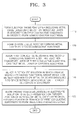
- FIG.. 3 is a flowchart illustrating a method of manufacturing the dye-sensitized solar cell 100 of FIG.. 1 , according to an embodiment of the present invention.
- a metal oxide layer 14 onto which a dye molecule layer 16 is adsorbed is formed on a first conductive substrate 12.
- the first conductive substrate 12 on which the metal oxide layer 14 is formed is prepared.
- the metal oxide layer 14 may be formed to a thickness of 5 to 15 ⁇ m.
- the dye molecule layer 16 is coated on a surface of the metal oxide layer 14 by immersing the first conductive substrate 12 on which the metal oxide layer 14 is formed in a dye solution composed of a ruthenium complex for 24 hours or more.
- the resultant structure on which the dye molecule layer 16 is formed is dried in an N 2 atmosphere to remove an alcohol-based organic solvent from a surface of the resultant structure.
- a portion of the surface of the metal oxide layer 14 onto which the dye molecule layer 16 is not adsorbed may be exposed. Also, a portion of a surface of the first conductive substrate 12 which does not contact the metal oxide layer 14 may be exposed.
- the first conductive substrate 12 and the second conductive substrate 22 are aligned with each other so that the electron transport layer 13 formed on the first conductive substrate 12 can face the metal layer 24 of the opposite electrode 20 formed on the second conductive substrate 22.
- a polymer layer 40 which may have a thickness of about 30 to 50 ⁇ m and may be formed of SURLYN (manufactured by Du Pont), is interposed between the first conductive substrate 12 and the second conductive substrate 22, and the first conductive substrate 12 and the second conductive substrate 22 are attached to each other on a heating plate at a temperature of 100 to 140°C under an atmospheric pressure of 1 to 3 such that a relatively small gap is formed between the first conductive substrate 12 and the second conductive substrate 22. Due to heat and pressure, the polymer layer 40 is strongly attached onto surfaces of both the semiconductor electrode 10 and the opposite electrode 20.
- an electrolyte solution 30 is injected through a micro hole 26 formed in the second conductive substrate 22 into a space between the semiconductor electrode 10 and the opposite electrode 20.
- Organic molecules having a functional group which can be selectively self-assembled on a metal oxide by a chemical bond with the metal oxide are dissolved in the electrolyte solution 30.
- the organic molecules dissolved in the electrolyte solution 30 are self-assembled on at least one of the exposed portion of the surface of the metal oxide layer 14 and on the exposed portion of the surface of the first conductive substrate12 to form an insulating protective layer 18.
- the organic molecules dissolved in the electrolyte solution 30 may be selected from insulating organic materials that cannot transport electrons or holes.
- the organic molecules may be selected from organic molecules having a functional group which can be selectively self-assembled by a chemical bond only on a surface of a metal oxide.
- the organic molecules may include a silane compound, a phosphate compound, a sulfuric acid compound, or a carboxylic acid compound.
- the silane compound When a silane compound is used as the source material of the organic molecules, the silane compound may have a structure selected from the group consisting of R 1 SiHR 2 R 3 , R 1 SiXR 2 R 3 (X is Cl, Br, or I), and R 1 SiRR 2 R 3 (R is methoxy, ethoxy, or t- butoxy), where R 1 , R 2 , and R 3 are a C 1 -C 24 alkane, an alkene, or alkynes, and each of R 1 , R 2 , and R 3 is substituted or unsubstituted with fluorine.
- the silane compound may be alkylsilane, alkyltrichlorosilane, alkoxy alkylsilane, trialkoxy alkylsilane, or dialkoxy dialkylsilane including a C 1 -C 24 alkyl group or alkoxy group.
- the phosphate compound may have a functional group selected from -PO 4 , -PO 3 , -PO 2 , and - PO.
- the phosphate compound may have a structure of PR 1 R 2 R 3 R 4 , where R 1 , R 2 , R 3 , and R 4 are C 1 -C 24 alkane, alkene, or alkynes, each of R 1 , R 2 , R 3 and R 4 is substituted or unsubstituted with fluorine, and at least one of R 1 , R 2 , R 3 , and R 4 is -OH or -O.
- the phosphate compound may exist in the form of a complex having a metal ion.
- the phosphate compound may be an alkyl phosphoric acid, alkyl hyposphorous acid, or phosphorous acid having a C 1 -C 24 alkyl group substituted or unsubstituted with fluorine.
- the sulfuric acid compound may have a functional group selected from -SO 4 , -SO 3 , -SO 2 , and -SO.
- the sulfuric acid compound may have a structure of SR 1 R 2 R 3 R 4 , where R 1 , R 2 , R 3 , and R 4 are C 1 -C 24 alkane, alkene, or alkynes, each of R 1 , R 2 , R 3 and R 4 is substituted or unsubstituted with fluorine, and at least one of R 1 , R 2 , R 3 , and R 4 is -OH or -O.
- the sulfuric acid compound may exist in forms of a complex having a metal ion.
- the sulfuric acid compound may be sulfuric acid, sulfurous acid, or a metal-ion complex thereof, i.e., sodium sulfate and potassium sulfite.
- the carboxylic acid compound When a carboxylic acid compound is used as the source material of the organic molecules, the carboxylic acid compound may have a functional group of -COOH or -COO - .
- the carboxylic acid compound may have a structure of R 1 COOH or R 2 COO - , where R 1 and R 2 are C 1 -C 24 alkane, alkene, or alkynes, and each of R 1 and R 2 is substituted or unsubstituted with fluorine.
- the carboxylic acid compound may be methanoic acid, ethanoic acid, propanoic acid, butanoic acid, malonic acid, oxalic acid, succinic acid, phthalic acid, glutaric acid, adipic acid, or benzoic acid.
- the electrolyte solution 30 contacts the electron transport layer 13 of the first conductive substrate 12 such that the organic molecules dissolved in the electrolyte solution 30 are self-assembled on the portion of the surface of the metal oxide layer 14 which is not covered by the dye molecule layer 16 and the portion of the surface of the first conductive substrate 12 which does not contact the metal oxide layer 14 to form the insulating protective layer 18. Due to the insulating protective layer 18, inefficient electron loss due to an interaction with the electrolyte solution 30 can be prevented when the electrons injected into the metal oxide layer 14 from the electron transport layer 13 are transported to the external circuit through the first conductive substrate 12.
- a first TiO 2 nano-particle layer was formed on a FTO substrate by screen printing using synthesized TiO 2 paste, and then was dried and sintered at a temperature of 500 °C.
- a second TiO 2 nano-particle layer including light scattering particles having a diameter of 200 to 400 nm was formed on the first TiO 2 nano-particle layer by screen printing ,and then was dried and sintered to manufacture a TiO 2 thin film in the form of a double-layered structure having a thickness of 20 ⁇ m.
- the resultant structure on which the TiO 2 thin film was formed was added to an alcoholic solution in which ruthenium dye (4,4'-dicarboxy-2,2-bupyridine)bis(thiocyanato)ruthenium(II): N3) was dissolved, and the dye was adsorbed onto a surface of the TiO 2 thin film.
- the resultant structure onto which the dye was adsorbed was washed using ethanol and dried to form a semiconductor electrode.
- a conductive glass substrate on which a H 2 PtCl 6 solution was coated was heated for 30 minutes at a temperature 450 °C to prepare counter electrodes.
- the semiconductor electrodes and the counter electrodes were aligned so their respective conductive surfaces faced each other. Then, a polymer layer formed of SURLYN (manufactured by Du Pont) was interposed between the semiconductor electrodes and the counter electrodes to adhere the semiconductor electrodes and the counter electrodes together so that a relatively small gap was formed therebetween. Samples prepared after performing such a process were divided into three groups.
- I 3 - /I - electrolyte solutions having different compositions were injected into spaces between the semiconductor electrodes and the counter electrodes in the prepared three groups of samples to complete the manufacture of dye-sensitized solar cells.
- the compositions of the electrolyte solutions injected into the samples are shown in Table 1 below.
- Table 1 Constituent Lil (M) MBII (M) I 2 (M) t-bPyridine (M) guanidinium thiocyanate (M) Sample 1 0.02 0.6 0.04 0.28 0.05 Sample 2 - 0.6 0.03 0.5 0.1 Sample 3 0.04 0.005 0.02 0.5 -
- MBII denotes methylbuthylimidazolium iodide
- t-bPyridine denotes tertiary buthylpyridine.
- guanidinium thiocyanate As shown in Table 1, 0.05 M guanidinium thiocyanate and 0.1 M guanidinium thiocyanate were added as organic molecules respectively to the electrolyte solutions injected into Sample 1 and Sample 2.
- the guanidinium thiocyanate was self-assembled on a portion of the TiO 2 thin film which does not allow dye adsorption and thus contacts the electrolyte solution and on a portion of the FTO substrate which does not contact the TiO 2 thin film and thus contacts the electrolyte solution to form an insulating protective layer.
- V oc denotes an open-circuit voltage
- J sc denotes a short-circuit current
- FF denotes a fill factor
- Eff denotes efficiency.
- Samples 1 and 2 into which the electrolyte solutions including the organic molecules which are self-assembled on the surface of the TiO 2 thin film and on the surface of the FTO substrate to form the insulating protective layers are injected have higher open-circuit voltages and higher efficiency than Sample 3 into which the electrolyte solution not including the organic molecules is injected.
- an insulating protective layer is formed on a surface of a metal oxide layer which can contact an oxidation/reduction electrolyte, and on a surface of a conductive substrate, electron loss easily occurring when electrons generated by the photovoltaic effect are transported to an external circuit can be prevented, thereby significantly improving energy conversion efficiency.
Landscapes
- Engineering & Computer Science (AREA)
- Power Engineering (AREA)
- Microelectronics & Electronic Packaging (AREA)
- Hybrid Cells (AREA)
- Photovoltaic Devices (AREA)
Abstract
Description
- This application claims the benefit of Korean Patent Application No.
10-2007-0083952, filed on August 21, 2007 - The present invention relates to a solar cell and a method of manufacturing the same, and more particularly, to a dye-sensitized solar cell including a metal oxide layer on which dye molecules are coated and a method of manufacturing the dye-sensitized solar cell. This work was supported by the IT R&D program of MIC/IITA. [2006-S-006-02, Components/Module technology for Ubiquitous Terminals]
- Unlike conventional p-n junction silicon solar cells, dye-sensitized solar cells are photo-electrochemical solar cells that primarily use photosensitive dye molecules capable of generating electron-hole pairs by absorbing visible light, and a transition metal oxide transporting the generated electrons. Graetzel cells disclosed in
U.S. Patent Nos. 4,927,721 and5,350,644, issued to Graetzel et al . (Switzerland) are representative dye-sensitized solar cells. These dye-sensitized solar cells are photo-electrochemical solar cells that include a semiconductor electrode formed of a nanoparticle titanium dioxide (TiO2) layer onto which dye molecules are adsorbed, an opposite electrode coated with platinum or carbon, and an electrolyte solution filled between the semiconductor electrode and the opposite electrode. The dye-sensitized solar cells can offer lower manufacturing costs per unit of power than conventional silicon solar cells and thus have attracted widespread interest as promising substitutes for conventional solar cells. - The principle of operation of the dye-sensitized solar cells will now be explained. Electrons are injected into a conduction band of the nanoparticle TiO2 layer from photosensitive dyes excited by sunlight. The injected electrons pass through the nanoparticle TiO2 layer to reach a conductive substrate and are transported to an external circuit. After performing electrical work in the external circuit, the electrons are transported back into the nanoparticle TiO2 layer through the opposite electrode by an oxidation/reduction electrolyte so as to reduce photosensitive dyes having insufficient electrons, thereby completing the operation of the dye-sensitized solar cells. Here, when the electrons injected from the photosensitive dyes pass through the nanoparticle TiO2 layer and the conductive substrate before reaching the external circuit, some of the injected electrons may remain in an empty surface energy level on the surface of the nanoparticle TiO2 layer.. If there is a portion of the surface of the nanoparticle TiO2 layer onto which the photosensitive dyes are not adsorbed and thus which is exposed to the electrolyte solution, or if there is a portion of the surface of the conductive substrate constituting the semiconductor electrode which does not contact the nanoparticle TiO2 layer and thus is exposed to the electrolyte solution, the electrons remaining in the empty surface energy level react with the oxidation/reduction electrolyte, and are removed inefficiently instead of moving through the circuit. In addition, the electrons generated by light may also react with the oxidation/reduction electrolyte and may be removed on the surface of the conductive substrate, thereby decreasing energy conversion efficiency.
- The present invention provides a dye-sensitized solar cell that can prevent electron loss due to an interaction between an oxidation/reduction electrolyte and electrons injected from photosensitive dyes on a surface of a metal oxide layer or on a surface of a conductive substrate.
- The present invention also provides a method of manufacturing a dye-sensitized solar cell which can prevent electron loss due to an interaction between an oxidation/reduction electrolyte and electrons injected from photosensitive dyes on a surface of a metal oxide layer or on a surface of a conductive substrate.
- According to an aspect of the present invention, there is provided a dye-sensitized solar cell comprising: a semiconductor electrode comprising: a metal oxide layer formed on a first conductive substrate; a dye molecule layer absorbed onto a surface of the metal oxide layer; and an insulating protective layer formed on at least one of a first portion of the surface of the metal oxide layer which is not covered by the dye molecule layer and a second portion of a surface of the first conductive substrate which does not contact the metal oxide layer; an opposite electrode disposed on a second conductive substrate and facing the semiconductor electrode; and an electrolyte solution filled in a space between the semiconductor electrode and the opposite electrode and including organic molecules having a functional group, which can be selectively self-assembled by a chemical bond with a metal oxide on the metal oxide, dissolved therein..
- The insulating protective layer may comprise a self-assembled molecule layer formed of an insulating organic material which is self-assembled by a chemical bond on at least one of the first portion and the second portion.
- According to another aspect of the present invention, there is provided a method of manufacturing a dye-sensitized solar cell, the method comprising: forming a semiconductor electrode comprising an electron transport layer that comprises a metal oxide layer disposed on a first conductive substrate and a dye molecule layer absorbed onto a surface of the metal oxide layer; forming an opposite electrode on a second conductive substrate; aligning the semiconductor electrode and the opposite electrode to face each other; and injecting an electrolyte solution in which organic molecules having a functional group which can be selectively self-assembled by a chemical bond with a metal oxide on the metal oxide are dissolved into a space between the semiconductor electrode and the opposite electrode and contacting the electrolyte solution with the electron transport layer.
- The semiconductor electrode may comprise a first portion of the surface of the metal oxide layer which is not covered by the dye molecule layer and a second portion of a surface of the first conductive substrate which does not contact the metal oxide layer, wherein the contacting of the electrolyte solution with the electron transport layer comprises self-assembling the organic molecules dissolved in the electrolyte solution on at least one of the first portion and the second portion so that an insulating protective layer can be formed on at least one of the first portion and the second portion.
- The organic molecules may comprise at least one selected from the group consisting of a silane compound, a phosphate compound, a sulfuric acid compound, and a carboxylic acid compound.
- The above and other features and advantages of the present invention will become more apparent by describing in detail exemplary embodiments thereof with reference to the attached drawings in which:
-
FIG. 1 is a cross-sectional view of a dye-sensitized solar cell according to an embodiment of the present invention; -
FIG. 2 is an enlarged cross-sectional view of a semiconductor electrode of the dye-sensitized solar cell ofFIG. 1 , according to an embodiment of the present invention; and -
FIG. 3 is a flowchart illustrating a method of manufacturing the dye-sensitized solar cell ofFIG. 1 , according to an embodiment of the present invention. - The present invention will now be described more fully with reference to the accompanying drawings, in which exemplary embodiments of the invention are shown.
- The invention may, however, be embodied in different forms and should not be construed as limited to the embodiments set forth herein. Rather, these embodiments are provided so that this disclosure will be thorough and complete, and will fully convey the scope of the invention to those skilled in the art. In the drawings, the thicknesses of layers and regions and the sizes of components may be exaggerated for clarity.
-
FIG. 1 is a cross-sectional view of a dye-sensitizedsolar cell 100 according to an embodiment of the present invention. - Referring to
FIG.. 1 , the dye-sensitizedsolar cell 100 according to the current embodiment of the present invention includes asemiconductor electrode 10, an opposite electrode 20 facing thesemiconductor electrode 10, and anelectrolyte solution 30 filled between thesemiconductor electrode 10 and the opposite electrode 20. - Organic molecules having a functional group which can be selectively self-assembled by a chemical bond with a metal oxide on the metal oxide are dissolved in the
electrolyte solution 30. The organic molecules dissolved in theelectrolyte solution 30 may be formed of a silane compound, a phosphate compound, a sulfuric acid compound, or a carboxylic acid compound. This will be explained later in detail. -
FIG. 2 is an enlarged cross-sectional view of thesemiconductor electrode 10 of the dye-sensitizedsolar cell 100 ofFIG. 1 , according to an embodiment of the present invention. - Referring to
FIGS.. 1 and 2 , thesemiconductor electrode 10 according to the current embodiment of the present invention includes a transparent firstconductive substrate 12, and anelectron transport layer 13 formed on the firstconductive substrate 12 to transport electrons to the firstconductive substrate 12. Theelectron transport layer 13 includes ametal oxide layer 14 formed on the firstconductive substrate 12, and adye molecule layer 16 adsorbed onto a surface of themetal oxide layer 14. - An insulating
protective layer 18 for preventing inefficient electron loss due to an interaction with theelectrolyte solution 30 is formed on a portion of the surface of themetal oxide layer 14 which is not covered by thedye molecule layer 16 and on a portion of a surface of the firstconductive substrate 12 which does not contact themetal oxide layer 14. The insulatingprotective layer 18 is formed of an insulating organic material having no capacity to transport electrons or holes. The insulatingprotective layer 18 may be formed of an organic material self-assembled on the surface of themetal oxide layer 14 and on the surface of the firstconductive substrate 12. In particular, the insulatingprotective layer 18 may include a self-assembled molecule layer formed by self-assembling the organic molecules dissolved in theelectrolyte solution 30 on the surface of themetal oxide layer 14 and on the surface of the firstconductive substrate 12. The insulatingprotective layer 18 may be formed of a silane compound, a phosphate compound, a sulfuric acid compound, or a carboxylic acid compound. This will be explained later in detail. - The first
conductive substrate 12 may be formed of indium tin oxide (ITO), fluorine-doped tin oxide (FTO), or a glass substrate on which SnO2 is coated. - The
metal oxide layer 14 may be formed of titanium dioxide (TiO2), tin-dioxide (SnO2), zinc oxide (ZnO), or a combination thereof. Themetal oxide layer 14 may have a thickness of about 5 to 15 µm. - The
dye molecule layer 16 may be formed of a ruthenium complex. - The insulating
protective layer 18 including a self-assembled molecule layer formed by self-assembling the organic molecules dissolved in theelectrolyte solution 30 on the surface of themetal oxide layer 14 and on the surface of the first conductive substrate 12may be a one-molecule layer. The thickness of the insulatingprotective layer 18 may be adjusted according to the molecular length of materials forming the one-molecular layer. - The source compound of the self-assembled molecule layer may be selected from organic molecules having a functional group which can be selectively self-assembled by a chemical bond on a metal oxide. In this regard, the organic molecules may include a silane compound, a phosphate compound, a sulfuric acid compound, or a carboxylic acid compound. As described above, the self-assembled molecule layer may be formed of the organic molecules dissolved in the
electrolyte solution 30. The insulatingprotective layer 18 may be formed when theelectrolyte solution 30 in which the organic molecules are dissolved contacts at least one of the surface of themetal oxide layer 14 and the surface of the firstconductive substrate 12 and the organic molecules dissolved in theelectrolyte solution 30 are self-assembled on at least one of the surface of themetal oxide layer 14 and the surface of the firstconductive substrate 12. The organic molecules constituting the self-assembled molecule layer will be explained later in detail. - Referring back to
FIG. 1 , the opposite electrode 20 includes a second conductive substrate 22 and ametal layer 24 coated on the second conductive substrate 22. Themetal layer 24 may be a platinum layer. The conductive substrate 22 may be formed of ITO, FTO, or a glass substrate on which SnO2 is coated. - The
metal layer 24 of the opposite electrode 20 is disposed to face theelectron transport layer 13 of thesemiconductor electrode 10. - The
electrolyte solution 30 filled in a space between thesemiconductor electrode 10 and the opposite electrode 20 may include an imidazole-based compound and iodine. For example, theelectrolyte solution 30 may include a I3 -/I- electrolyte solution composed of 0.70 M 1-vinyl-3-methyl-immidazolium iodide, 0.10 M Lil, 40 mM iodine (I2), and 0.125 M 4-tert-butylpyridine in 3-methoxypropionitrile. - The organic molecules having a functional group which can be selectively self-assembled on the
metal oxide layer 14 by a chemical bond with the metal oxide are dissolved in theelectrolyte solution 30 as described above. The organic molecules dissolved in theelectrolyte solution 30 may be formed of a silane compound, a phosphate compound, a sulfuric acid compound, or a carboxylic acid compound. - The concentration of the organic molecules in the total amount of the
electrolyte solution 30 may be about 0.001 to 1 M. - The
electrolyte solution 30 is injected through amicro hole 26 formed in the second conductive substrate 22 of the opposite electrode 20 into the space defined by apolymer layer 40 between thesemiconductor electrode 10 and the opposite electrode 20. - The operation of the dye-sensitized
solar cell 100 ofFIG. 1 constructed as described above will now be explained. - When sunlight which penetrates the first
conductive substrate 12 of thesemiconductor electrode 10 is absorbed into thedye molecule layer 16 adsorbed onto themetal oxide layer 14, materials of thedye molecule layer 16 are excited and thus electrons are injected into a conduction band of themetal oxide layer 14. The electrons injected into themetal oxide layer 14 are delivered to the firstconductive substrate 12, which contacts themetal oxide layer 14, through an interface between nano-scale fine particles constituting themetal oxide layer 14 and then are transported to the opposite electrode 20 through an external electric wire (not shown). - The
dye molecule layer 16, which is oxidized as a result of an electron transition, receives electrons provided by an oxidation-reduction action (3I- → I3 - + 2e-) of iodine ions disposed in theelectrolyte solution 30 and the electrons are reduced again. The oxidized iodine ions (I3 -) are reduced again by the electrons reaching the opposite electrode 20, thereby completing the operation of the dye-sensitizedsolar cell 100. - As described above, in the operation of the dye-sensitized
solar cell 100, since the portion of the firstconductive substrate 12 of thesemiconductor electrode 10 which does not contact themetal oxide layer 14 and the portion of themetal oxide layer 14 of thesemiconductor electrode 10 which is not covered by thedye molecule layer 16 are covered by the insulatingprotective layer 18, a path through which electron loss easily occurs cannot be formed due to the insulatingprotective layer 18 and thus energy conversion efficiency can be improved significantly. -
FIG.. 3 is a flowchart illustrating a method of manufacturing the dye-sensitizedsolar cell 100 ofFIG.. 1 , according to an embodiment of the present invention. - In
operation 110, in order to form asemiconductor electrode 10 including anelectron transport layer 13, ametal oxide layer 14 onto which adye molecule layer 16 is adsorbed is formed on a firstconductive substrate 12. - To this end, the first
conductive substrate 12 on which themetal oxide layer 14 is formed is prepared. Themetal oxide layer 14 may be formed to a thickness of 5 to 15 µm. Thedye molecule layer 16 is coated on a surface of themetal oxide layer 14 by immersing the firstconductive substrate 12 on which themetal oxide layer 14 is formed in a dye solution composed of a ruthenium complex for 24 hours or more. - The resultant structure on which the
dye molecule layer 16 is formed is dried in an N2 atmosphere to remove an alcohol-based organic solvent from a surface of the resultant structure. - A portion of the surface of the
metal oxide layer 14 onto which thedye molecule layer 16 is not adsorbed may be exposed. Also, a portion of a surface of the firstconductive substrate 12 which does not contact themetal oxide layer 14 may be exposed. - In
operation 120, in order to form an opposite electrode 20, ametal layer 24, e.g., a platinum layer, is coated on a second conductive substrate 22. - In
operation 130, the firstconductive substrate 12 and the second conductive substrate 22 are aligned with each other so that theelectron transport layer 13 formed on the firstconductive substrate 12 can face themetal layer 24 of the opposite electrode 20 formed on the second conductive substrate 22. - To this end, a
polymer layer 40, which may have a thickness of about 30 to 50 µm and may be formed of SURLYN (manufactured by Du Pont), is interposed between the firstconductive substrate 12 and the second conductive substrate 22, and the firstconductive substrate 12 and the second conductive substrate 22 are attached to each other on a heating plate at a temperature of 100 to 140°C under an atmospheric pressure of 1 to 3 such that a relatively small gap is formed between the firstconductive substrate 12 and the second conductive substrate 22. Due to heat and pressure, thepolymer layer 40 is strongly attached onto surfaces of both thesemiconductor electrode 10 and the opposite electrode 20. - In
operation 140, anelectrolyte solution 30 is injected through amicro hole 26 formed in the second conductive substrate 22 into a space between thesemiconductor electrode 10 and the opposite electrode 20. Organic molecules having a functional group which can be selectively self-assembled on a metal oxide by a chemical bond with the metal oxide are dissolved in theelectrolyte solution 30. - After the injection of the
electrolyte solution 30, SURLYN and a thin glass are rapidly heated to close themicro hole 26. - In
operation 150, the organic molecules dissolved in theelectrolyte solution 30 are self-assembled on at least one of the exposed portion of the surface of themetal oxide layer 14 and on the exposed portion of the surface of the first conductive substrate12 to form an insulatingprotective layer 18. - In order to form the insulating
protective layer 18 as a self-assembled organic layer, the organic molecules dissolved in theelectrolyte solution 30 may be selected from insulating organic materials that cannot transport electrons or holes. In particular, the organic molecules may be selected from organic molecules having a functional group which can be selectively self-assembled by a chemical bond only on a surface of a metal oxide. In this regard, the organic molecules may include a silane compound, a phosphate compound, a sulfuric acid compound, or a carboxylic acid compound. - When a silane compound is used as the source material of the organic molecules, the silane compound may have a structure selected from the group consisting of R1SiHR2R3, R1SiXR2R3 (X is Cl, Br, or I), and R1SiRR2R3 (R is methoxy, ethoxy, or t- butoxy), where R1, R2, and R3 are a C1-C24 alkane, an alkene, or alkynes, and each of R1, R2, and R3 is substituted or unsubstituted with fluorine. For example, the silane compound may be alkylsilane, alkyltrichlorosilane, alkoxy alkylsilane, trialkoxy alkylsilane, or dialkoxy dialkylsilane including a C1-C24 alkyl group or alkoxy group.
- When a phosphate compound is used as the source material of the organic molecules, the phosphate compound may have a functional group selected from -PO4, -PO3, -PO2, and - PO. The phosphate compound may have a structure of PR1R2R3R4, where R1, R2, R3, and R4 are C1-C24 alkane, alkene, or alkynes, each of R1, R2, R3 and R4 is substituted or unsubstituted with fluorine, and at least one of R1, R2, R3, and R4 is -OH or -O. When at least one of R1, R2, R3, and R4 is -O, the phosphate compound may exist in the form of a complex having a metal ion. For example, the phosphate compound may be an alkyl phosphoric acid, alkyl hyposphorous acid, or phosphorous acid having a C1-C24 alkyl group substituted or unsubstituted with fluorine.
- When a sulfuric acid compound is used as the source material of the organic molecules, the sulfuric acid compound may have a functional group selected from -SO4, -SO3, -SO2, and -SO. The sulfuric acid compound may have a structure of SR1R2R3R4, where R1, R2, R3, and R4 are C1-C24 alkane, alkene, or alkynes, each of R1, R2, R3 and R4 is substituted or unsubstituted with fluorine, and at least one of R1, R2, R3, and R4 is -OH or -O. When at least one of R1, R2, R3, and R4 is -O, the sulfuric acid compound may exist in forms of a complex having a metal ion. For example, the sulfuric acid compound may be sulfuric acid, sulfurous acid, or a metal-ion complex thereof, i.e., sodium sulfate and potassium sulfite.
- When a carboxylic acid compound is used as the source material of the organic molecules, the carboxylic acid compound may have a functional group of -COOH or -COO-. The carboxylic acid compound may have a structure of R1COOH or R2COO-, where R1 and R2 are C1-C24 alkane, alkene, or alkynes, and each of R1 and R2 is substituted or unsubstituted with fluorine. For example, the carboxylic acid compound may be methanoic acid, ethanoic acid, propanoic acid, butanoic acid, malonic acid, oxalic acid, succinic acid, phthalic acid, glutaric acid, adipic acid, or benzoic acid.
- As described above, once the
electrolyte solution 30 is injected between the firstconductive substrate 12 and the second conductive substrate 22 inoperation 150, theelectrolyte solution 30 contacts theelectron transport layer 13 of the firstconductive substrate 12 such that the organic molecules dissolved in theelectrolyte solution 30 are self-assembled on the portion of the surface of themetal oxide layer 14 which is not covered by thedye molecule layer 16 and the portion of the surface of the firstconductive substrate 12 which does not contact themetal oxide layer 14 to form the insulatingprotective layer 18. Due to the insulatingprotective layer 18, inefficient electron loss due to an interaction with theelectrolyte solution 30 can be prevented when the electrons injected into themetal oxide layer 14 from theelectron transport layer 13 are transported to the external circuit through the firstconductive substrate 12. - An example of manufacturing a dye-sensitized solar cell according to the present invention will now be described in detail.
- A first TiO2 nano-particle layer was formed on a FTO substrate by screen printing using synthesized TiO2 paste, and then was dried and sintered at a temperature of 500 °C. A second TiO2 nano-particle layer including light scattering particles having a diameter of 200 to 400 nm was formed on the first TiO2 nano-particle layer by screen printing ,and then was dried and sintered to manufacture a TiO2 thin film in the form of a double-layered structure having a thickness of 20 µm.
- The resultant structure on which the TiO2 thin film was formed was added to an alcoholic solution in which ruthenium dye (4,4'-dicarboxy-2,2-bupyridine)bis(thiocyanato)ruthenium(II): N3) was dissolved, and the dye was adsorbed onto a surface of the TiO2 thin film.. The resultant structure onto which the dye was adsorbed was washed using ethanol and dried to form a semiconductor electrode.
- A conductive glass substrate on which a H2PtCl6 solution was coated was heated for 30 minutes at a temperature 450 °C to prepare counter electrodes.
- The semiconductor electrodes and the counter electrodes were aligned so their respective conductive surfaces faced each other. Then, a polymer layer formed of SURLYN (manufactured by Du Pont) was interposed between the semiconductor electrodes and the counter electrodes to adhere the semiconductor electrodes and the counter electrodes together so that a relatively small gap was formed therebetween. Samples prepared after performing such a process were divided into three groups.
- Next, I3 -/I- electrolyte solutions having different compositions were injected into spaces between the semiconductor electrodes and the counter electrodes in the prepared three groups of samples to complete the manufacture of dye-sensitized solar cells. The compositions of the electrolyte solutions injected into the samples are shown in Table 1 below.
Table 1 Constituent Lil (M) MBII (M) I2 (M) t-bPyridine (M) guanidinium thiocyanate (M) Sample 1 0.02 0.6 0.04 0.28 0.05 Sample 2 - 0.6 0.03 0.5 0.1 Sample 3 0.04 0.005 0.02 0.5 - - In Table 1, MBII denotes methylbuthylimidazolium iodide, t-bPyridine denotes tertiary buthylpyridine.
- As shown in Table 1, 0.05 M guanidinium thiocyanate and 0.1 M guanidinium thiocyanate were added as organic molecules respectively to the electrolyte solutions injected into Sample 1 and Sample 2. The guanidinium thiocyanate was self-assembled on a portion of the TiO2 thin film which does not allow dye adsorption and thus contacts the electrolyte solution and on a portion of the FTO substrate which does not contact the TiO2 thin film and thus contacts the electrolyte solution to form an insulating protective layer.
- No guanidinium thiocyanate was added to Sample 3.
- In order to evaluate light conversion efficiency of the dye-sensitized solar cells of Samples 1 through 3 manufactured in Example 1, photo voltages and photo currents of the dye-sensitized solar cells were measured as follows To this end, a solar simulator including a source meter (Keithley 2400 SourceMeter®) was used. Here, a Xenon lamp (Oriel, 91193) was used as a light source.
- Voltages and short-circuit currents of the dye-sensitized solar cells of Samples 1 through 3 manufactured in Example 1 were measured and the results are shown in Table 2 below.
Table 2 Characteristics Voc(V) Jsc (mA/cm2) FF Eff (%) Sample 1 0.77 11 72 6.1 Sample 2 0.81 11.25 74 6.74 Sample 3 0.74 11.3 55 4.43 - In Table 2, Voc denotes an open-circuit voltage, Jsc denotes a short-circuit current, FF denotes a fill factor, and Eff denotes efficiency.
- As shown in Table 2, Samples 1 and 2 into which the electrolyte solutions including the organic molecules which are self-assembled on the surface of the TiO2 thin film and on the surface of the FTO substrate to form the insulating protective layers are injected have higher open-circuit voltages and higher efficiency than Sample 3 into which the electrolyte solution not including the organic molecules is injected.
- As described above, according to the dye-sensitized solar cell of the present invention, since an insulating protective layer is formed on a surface of a metal oxide layer which can contact an oxidation/reduction electrolyte, and on a surface of a conductive substrate, electron loss easily occurring when electrons generated by the photovoltaic effect are transported to an external circuit can be prevented, thereby significantly improving energy conversion efficiency.
- While the present invention has been particularly shown and described with reference to exemplary embodiments thereof, it will be understood by those of ordinary skill in the art that various changes in form and details may be made therein without departing from the spirit and scope of the present invention as defined by the following claims.
Claims (15)
- A dye-sensitized solar cell comprising:a semiconductor electrode comprising:a metal oxide layer formed on a first conductive substrate;a dye molecule layer absorbed onto a surface of the metal oxide layer; andan insulating protective layer formed on at least one of a first portion of the surface of the metal oxide layer which is not covered by the dye molecule layer and a second portion of a surface of the first conductive substrate which does not contact the metal oxide layer;an opposite electrode disposed on a second conductive substrate and facing the semiconductor electrode; andan electrolyte solution filled in a space between the semiconductor electrode and the opposite electrode and including organic molecules having a functional group, which can be selectively self-assembled by a chemical bond with a metal oxide on the metal oxide, dissolved therein.
- The dye-sensitized solar cell of claim 1, wherein the insulating protective layer comprises a self-assembled molecule layer formed of an insulating organic material which is self-assembled by a chemical bond on at least one of the first portion and the second portion.
- The dye-sensitized solar cell of claim 2, wherein the insulating protective layer comprises a self-assembled molecule layer formed of at least one compound selected from the group consisting of a silane compound, a phosphate compound, a sulfuric acid compound, and a carboxylic acid compound each of which is self-assembled on at least one of the first portion and the second portion.
- The dye-sensitized solar cell of claim 3, wherein the compound has the same structure as that of the organic molecules dissolved in the electrolyte solution.
- The dye-sensitized solar cell of any of the preceding claims, wherein the organic molecules dissolved in the electrolyte solution comprise a silane compound having a structure selected from the group consisting of R1SiHR2R3, R1SiXR2R3 (X is Cl, Br, or I), and R1SiRR2R3 (R is methoxy, ethoxy, or t-butoxy), where R1, R2, and R3 are C1-C24 alkane, alkene, or alkynes, and each of R1, R2, and R3 is substituted or unsubstituted with fluorine.
- The dye-sensitized solar cell of any of the preceding claims, wherein the organic molecules dissolved in the electrolyte solution comprise a phosphate compound having a structure PR1R2R3R4, where R1, R2, R3, and R4 are C1-C24 alkane, alkene, or alkynes, each of R1, R2, R3, and R4 is substituted or unsubstituted with fluorine, and at least one of R1, R2, R3, and R4 is -OH or -O.
- The dye-sensitized solar cell of any of the preceding claims, wherein the organic molecules dissolved in the electrolyte solution comprise a sulfuric acid compound having a structure of SR1R2R3R4, where R1, R2, R3, and R4 are a C1 - C24 alkane, an alkene, or alkynes, each of R1, R2, R3, and R4 is substituted or unsubstituted with fluorine, and at least one of R1, R2, R3, and R4 is -OH or -O.
- The dye-sensitized solar cell of any of the preceding claims, wherein the organic molecules dissolved in the electrolyte solution comprise a carboxylic acid compound having a structure of R1COOH or R2COO-, where R1 and R2 are a C1 - C24 alkane, an alkene, or alkynes, and each of R1 and R2 is substituted or unsubstituted with fluorine.
- The dye-sensitized solar cell of any of the preceding claims, wherein each of the first conductive substrate and the second conductive substrate is formed of indium tin oxide (ITO), fluorine-doped tin oxide (FTO), or a glass substrate on which SnO2 is coated.
- The dye-sensitized solar cell of any of the preceding claims, wherein the dye molecule layer is formed of a ruthenium complex.
- The dye-sensitized solar cell of any of the preceding claims, wherein the semiconductor oxide layer is formed of titanium dioxide (TiO2), tin-dioxide (SnO2), zinc oxide (ZnO), or a combination thereof.
- The dye-sensitized solar cell of any of the preceding claims, wherein the opposite electrode comprises a metal layer.
- A method of manufacturing a dye-sensitized solar cell, the method comprising:forming a semiconductor electrode comprising an electron transport layer that comprises a metal oxide layer disposed on a first conductive substrate and a dye molecule layer absorbed onto a surface of the metal oxide layer;forming an opposite electrode on a second conductive substrate;aligning the semiconductor electrode and the opposite electrode to face each other; andinjecting an electrolyte solution in which organic molecules having a functional group which can be selectively self-assembled by a chemical bond with a metal oxide on the metal oxide are dissolved into a space between the semiconductor electrode and the opposite electrode and contacting the electrolyte solution with the electron transport layer.
- The method of claim 13, wherein the semiconductor electrode comprises a first portion of the surface of the metal oxide layer which is not covered by the dye molecule layer, and a second portion of a surface of the first conductive substrate which does not contact the metal oxide layer,
wherein the contacting of the electrolyte solution with the electron transport layer comprises self-assembling the organic molecules dissolved in the electrolyte solution on at least one of the first portion and the second portion so that an insulating protective layer can be formed on at least one of the first portion and the second portion. - The method of claim 13 or 14, wherein the organic molecules comprise at least one selected from the group consisting of a silane compound, a phosphate compound, a sulfuric acid compound, and a carboxylic acid compound.
Applications Claiming Priority (1)
| Application Number | Priority Date | Filing Date | Title |
|---|---|---|---|
| KR1020070083952A KR100932901B1 (en) | 2007-08-21 | 2007-08-21 | Dye-Sensitized Solar Cell and Manufacturing Method Thereof |
Publications (2)
| Publication Number | Publication Date |
|---|---|
| EP2028667A2 true EP2028667A2 (en) | 2009-02-25 |
| EP2028667A3 EP2028667A3 (en) | 2011-11-02 |
Family
ID=39512840
Family Applications (1)
| Application Number | Title | Priority Date | Filing Date |
|---|---|---|---|
| EP08154241A Withdrawn EP2028667A3 (en) | 2007-08-21 | 2008-04-09 | Dye-sensitized solar cell and method of manufacturing the same |
Country Status (2)
| Country | Link |
|---|---|
| EP (1) | EP2028667A3 (en) |
| KR (1) | KR100932901B1 (en) |
Cited By (7)
| Publication number | Priority date | Publication date | Assignee | Title |
|---|---|---|---|---|
| CN101901845A (en) * | 2009-05-27 | 2010-12-01 | Tdk株式会社 | Metal oxide electrode, manufacturing method thereof, and dye-sensitized solar cell |
| ES2370856A1 (en) * | 2009-10-30 | 2011-12-23 | Everlight Usa, Inc. | ELECTROLYTIC COMPOSITION AND SOLAR CELL SENSITIZED BY COLOR USING THE SAME. |
| ES2376325A1 (en) * | 2009-11-05 | 2012-03-13 | Everlight Usa, Inc. | Electrolyte composition and dye-sensitized solar cell having the same |
| EP2230677A3 (en) * | 2009-03-13 | 2012-08-29 | DMS Co., Ltd. | Method and apparatus for production of dye-sensitized solar cells (DSSC) |
| CN103779101A (en) * | 2014-01-07 | 2014-05-07 | 浙江大学 | Hybrid solid solar cell and preparation method thereof |
| CN107068407A (en) * | 2017-01-03 | 2017-08-18 | 武汉市三选科技有限公司 | DSSC and its manufacture method |
| JP2019149583A (en) * | 2019-06-12 | 2019-09-05 | シャープ株式会社 | Dye-sensitized solar cell and electronic apparatus including dye-sensitized solar cell |
Families Citing this family (3)
| Publication number | Priority date | Publication date | Assignee | Title |
|---|---|---|---|---|
| KR101286075B1 (en) * | 2011-04-04 | 2013-07-15 | 포항공과대학교 산학협력단 | Dye-sensitized solar cells and manufacturing methods thereof |
| KR101225901B1 (en) * | 2011-05-31 | 2013-01-24 | 단국대학교 산학협력단 | Manufacturng method for organic solar cell and electrode of organic solar cell and organic solar cell and electrode of organic solar cell manufactured by the same |
| KR101531536B1 (en) * | 2012-09-12 | 2015-07-07 | 한국화학연구원 | Organic / hybrid solar cell with top photoactive layer controlled in shape and porosity |
Citations (2)
| Publication number | Priority date | Publication date | Assignee | Title |
|---|---|---|---|---|
| US4927721A (en) | 1988-02-12 | 1990-05-22 | Michael Gratzel | Photo-electrochemical cell |
| US5350644A (en) | 1990-04-17 | 1994-09-27 | Ecole Polytechnique, Federale De Lausanne | Photovoltaic cells |
Family Cites Families (7)
| Publication number | Priority date | Publication date | Assignee | Title |
|---|---|---|---|---|
| JP2000323192A (en) * | 1999-03-10 | 2000-11-24 | Fuji Xerox Co Ltd | Semiconductor electrode and photoelectric conversion element utilizing the electrode |
| EP1473745A1 (en) * | 2003-04-30 | 2004-11-03 | Ecole Polytechnique Federale De Lausanne (Epfl) | Dye sensitized solar cell |
| KR20040093515A (en) * | 2003-04-30 | 2004-11-06 | 기산비티시(주) | Improved Solar Perfomance of Dye Sensitized Solar Cell Using Secondary Oxide Thin Layer |
| EP1622178A1 (en) * | 2004-07-29 | 2006-02-01 | Ecole Polytechnique Federale De Lausanne (Epfl) | 2,2 -Bipyridine ligand, sensitizing dye and dye sensitized solar cell |
| JP5086807B2 (en) * | 2005-05-13 | 2012-11-28 | Agcセイミケミカル株式会社 | Novel amino group-containing heterocyclic derivative and sensitizing dye for photoelectric conversion containing the heterocyclic derivative |
| JP4509066B2 (en) * | 2005-07-08 | 2010-07-21 | シャープ株式会社 | Photosensitizer, semiconductor electrode and photoelectric conversion element |
| JP2007066526A (en) | 2005-08-29 | 2007-03-15 | Hitachi Ltd | Semiconductor electrode, dye-sensitized solar cell, and manufacturing method thereof |
-
2007
- 2007-08-21 KR KR1020070083952A patent/KR100932901B1/en not_active Expired - Fee Related
-
2008
- 2008-04-09 EP EP08154241A patent/EP2028667A3/en not_active Withdrawn
Patent Citations (2)
| Publication number | Priority date | Publication date | Assignee | Title |
|---|---|---|---|---|
| US4927721A (en) | 1988-02-12 | 1990-05-22 | Michael Gratzel | Photo-electrochemical cell |
| US5350644A (en) | 1990-04-17 | 1994-09-27 | Ecole Polytechnique, Federale De Lausanne | Photovoltaic cells |
Cited By (8)
| Publication number | Priority date | Publication date | Assignee | Title |
|---|---|---|---|---|
| EP2230677A3 (en) * | 2009-03-13 | 2012-08-29 | DMS Co., Ltd. | Method and apparatus for production of dye-sensitized solar cells (DSSC) |
| CN101901845A (en) * | 2009-05-27 | 2010-12-01 | Tdk株式会社 | Metal oxide electrode, manufacturing method thereof, and dye-sensitized solar cell |
| EP2256763A3 (en) * | 2009-05-27 | 2012-01-11 | TDK Corporation | Metal oxide electrode for dye-sensitized solar cell, dye-sensitized solar cell, and manufacturing method of metal oxide electrode |
| ES2370856A1 (en) * | 2009-10-30 | 2011-12-23 | Everlight Usa, Inc. | ELECTROLYTIC COMPOSITION AND SOLAR CELL SENSITIZED BY COLOR USING THE SAME. |
| ES2376325A1 (en) * | 2009-11-05 | 2012-03-13 | Everlight Usa, Inc. | Electrolyte composition and dye-sensitized solar cell having the same |
| CN103779101A (en) * | 2014-01-07 | 2014-05-07 | 浙江大学 | Hybrid solid solar cell and preparation method thereof |
| CN107068407A (en) * | 2017-01-03 | 2017-08-18 | 武汉市三选科技有限公司 | DSSC and its manufacture method |
| JP2019149583A (en) * | 2019-06-12 | 2019-09-05 | シャープ株式会社 | Dye-sensitized solar cell and electronic apparatus including dye-sensitized solar cell |
Also Published As
| Publication number | Publication date |
|---|---|
| KR20090019485A (en) | 2009-02-25 |
| KR100932901B1 (en) | 2009-12-22 |
| EP2028667A3 (en) | 2011-11-02 |
Similar Documents
| Publication | Publication Date | Title |
|---|---|---|
| EP1906417A2 (en) | Dye-sensitized solar cell and method of manufacturing the same | |
| EP2234133B1 (en) | photoelectric conversion element comprising semiconductor oxide particles | |
| KR100932901B1 (en) | Dye-Sensitized Solar Cell and Manufacturing Method Thereof | |
| JP5300735B2 (en) | Dye-sensitized solar cell module | |
| KR100947371B1 (en) | Multi-wavelength Absorption Nano Structure Dye-Sensitized Solar Cell and Manufacturing Method Thereof | |
| EP1605479A2 (en) | Flexible dye-sentitized solar cell using conducting metal substrate | |
| Kang et al. | Dye-sensitized TiO2 solar cells using polymer gel electrolytes based on PVdF-HFP | |
| JP2003264011A (en) | Dye-sensitive solar cells | |
| JPWO2008004556A1 (en) | Dye-sensitized solar cell module and manufacturing method thereof | |
| EP2073226A2 (en) | Dye-sensitized solar cell and method of manufacturing the same | |
| US20110174368A1 (en) | Composite electrolyte and the preparation method thereof, and dye-sensitized solar cell using the same | |
| KR101190002B1 (en) | Semiconductor electrode for dye-sensitized solar cell, preparation method thereof and dye-sensitized solar cell using the same | |
| EP2256763A2 (en) | Metal oxide electrode for dye-sensitized solar cell, dye-sensitized solar cell, and manufacturing method of metal oxide electrode | |
| JP5114499B2 (en) | Photoelectric conversion element | |
| KR100908243B1 (en) | Dye-Sensitized Solar Cell Including Electron Recombination Blocking Layer and Manufacturing Method Thereof | |
| JP4772311B2 (en) | Electrolyte composition, photoelectric conversion element and dye-sensitized solar cell using the same, and evaluation method for ionic liquid | |
| KR101006078B1 (en) | Solid nanocomposite electrolyte and solar cell using same | |
| WO2012086377A1 (en) | Dye-sensitized solar cell and dye-sensitized solar cell module, and processes for production of those | |
| WO2012053327A1 (en) | Dye-sensitized solar cell module and method for manufacturing same | |
| Maharjan | Comparative study of characteristics of dye sensitized solar cells fabricated using substrates coated with fluorine doped tin oxide and titanium | |
| EP3220399A1 (en) | Electrolyte for dye-sensitized photoelectric conversion elements for low luminance, and dye-sensitized photoelectric conversion element for low luminance using same | |
| AU2007202986B2 (en) | Electrolyte composition, and photoelectric converter and dye-sensitized solar cell using same | |
| KR100967090B1 (en) | Dye-Sensitized Solar Cell Using Carbon Nanotube Electrode and Manufacturing Method Thereof | |
| JP5005177B2 (en) | Dye-sensitized solar cell | |
| Syrový et al. | Printed DSSC Solar Cell with UV Cured Barrier Layer |
Legal Events
| Date | Code | Title | Description |
|---|---|---|---|
| PUAI | Public reference made under article 153(3) epc to a published international application that has entered the european phase |
Free format text: ORIGINAL CODE: 0009012 |
|
| AK | Designated contracting states |
Kind code of ref document: A2 Designated state(s): AT BE BG CH CY CZ DE DK EE ES FI FR GB GR HR HU IE IS IT LI LT LU LV MC MT NL NO PL PT RO SE SI SK TR |
|
| AX | Request for extension of the european patent |
Extension state: AL BA MK RS |
|
| PUAL | Search report despatched |
Free format text: ORIGINAL CODE: 0009013 |
|
| AK | Designated contracting states |
Kind code of ref document: A3 Designated state(s): AT BE BG CH CY CZ DE DK EE ES FI FR GB GR HR HU IE IS IT LI LT LU LV MC MT NL NO PL PT RO SE SI SK TR |
|
| AX | Request for extension of the european patent |
Extension state: AL BA MK RS |
|
| RIC1 | Information provided on ipc code assigned before grant |
Ipc: H01L 31/00 20060101ALI20110926BHEP Ipc: H01G 9/20 20060101AFI20110926BHEP |
|
| 17P | Request for examination filed |
Effective date: 20120308 |
|
| AKX | Designation fees paid |
Designated state(s): AT BE BG CH CY CZ DE DK EE ES FI FR GB GR HR HU IE IS IT LI LT LU LV MC MT NL NO PL PT RO SE SI SK TR |
|
| 17Q | First examination report despatched |
Effective date: 20121109 |
|
| STAA | Information on the status of an ep patent application or granted ep patent |
Free format text: STATUS: THE APPLICATION IS DEEMED TO BE WITHDRAWN |
|
| 18D | Application deemed to be withdrawn |
Effective date: 20130320 |