EP2028640A2 - Sich automatisch einstellende Hintergrundbeleuchtung und Pixelhelligkeit auf Anzeigetafeln - Google Patents
Sich automatisch einstellende Hintergrundbeleuchtung und Pixelhelligkeit auf Anzeigetafeln Download PDFInfo
- Publication number
- EP2028640A2 EP2028640A2 EP08160797A EP08160797A EP2028640A2 EP 2028640 A2 EP2028640 A2 EP 2028640A2 EP 08160797 A EP08160797 A EP 08160797A EP 08160797 A EP08160797 A EP 08160797A EP 2028640 A2 EP2028640 A2 EP 2028640A2
- Authority
- EP
- European Patent Office
- Prior art keywords
- brightness
- panel
- sensors
- pixel
- display panel
- Prior art date
- Legal status (The legal status is an assumption and is not a legal conclusion. Google has not performed a legal analysis and makes no representation as to the accuracy of the status listed.)
- Granted
Links
- 238000000034 method Methods 0.000 claims description 75
- 239000004973 liquid crystal related substance Substances 0.000 claims description 20
- 238000001914 filtration Methods 0.000 claims description 2
- 230000007613 environmental effect Effects 0.000 description 31
- 230000000694 effects Effects 0.000 description 13
- 230000001276 controlling effect Effects 0.000 description 12
- 230000001795 light effect Effects 0.000 description 9
- 238000013459 approach Methods 0.000 description 6
- 238000004519 manufacturing process Methods 0.000 description 6
- 238000005259 measurement Methods 0.000 description 6
- 230000001603 reducing effect Effects 0.000 description 5
- 238000012360 testing method Methods 0.000 description 4
- 239000003086 colorant Substances 0.000 description 3
- 238000010586 diagram Methods 0.000 description 3
- 238000005516 engineering process Methods 0.000 description 3
- 238000007796 conventional method Methods 0.000 description 2
- 230000003247 decreasing effect Effects 0.000 description 2
- 238000013461 design Methods 0.000 description 2
- 238000012545 processing Methods 0.000 description 2
- 241000702619 Porcine parvovirus Species 0.000 description 1
- 230000005540 biological transmission Effects 0.000 description 1
- 238000004364 calculation method Methods 0.000 description 1
- 238000004891 communication Methods 0.000 description 1
- 238000012937 correction Methods 0.000 description 1
- 230000009977 dual effect Effects 0.000 description 1
- 230000006870 function Effects 0.000 description 1
- 238000012986 modification Methods 0.000 description 1
- 230000004048 modification Effects 0.000 description 1
- 238000004803 parallel plate viscometry Methods 0.000 description 1
- 230000008447 perception Effects 0.000 description 1
- 229920000553 poly(phenylenevinylene) Polymers 0.000 description 1
- 238000007639 printing Methods 0.000 description 1
- 230000001105 regulatory effect Effects 0.000 description 1
Images






Classifications
-
- G—PHYSICS
- G09—EDUCATION; CRYPTOGRAPHY; DISPLAY; ADVERTISING; SEALS
- G09G—ARRANGEMENTS OR CIRCUITS FOR CONTROL OF INDICATING DEVICES USING STATIC MEANS TO PRESENT VARIABLE INFORMATION
- G09G3/00—Control arrangements or circuits, of interest only in connection with visual indicators other than cathode-ray tubes
- G09G3/20—Control arrangements or circuits, of interest only in connection with visual indicators other than cathode-ray tubes for presentation of an assembly of a number of characters, e.g. a page, by composing the assembly by combination of individual elements arranged in a matrix no fixed position being assigned to or needed to be assigned to the individual characters or partial characters
- G09G3/34—Control arrangements or circuits, of interest only in connection with visual indicators other than cathode-ray tubes for presentation of an assembly of a number of characters, e.g. a page, by composing the assembly by combination of individual elements arranged in a matrix no fixed position being assigned to or needed to be assigned to the individual characters or partial characters by control of light from an independent source
- G09G3/3406—Control of illumination source
- G09G3/342—Control of illumination source using several illumination sources separately controlled corresponding to different display panel areas, e.g. along one dimension such as lines
-
- G—PHYSICS
- G09—EDUCATION; CRYPTOGRAPHY; DISPLAY; ADVERTISING; SEALS
- G09G—ARRANGEMENTS OR CIRCUITS FOR CONTROL OF INDICATING DEVICES USING STATIC MEANS TO PRESENT VARIABLE INFORMATION
- G09G3/00—Control arrangements or circuits, of interest only in connection with visual indicators other than cathode-ray tubes
- G09G3/20—Control arrangements or circuits, of interest only in connection with visual indicators other than cathode-ray tubes for presentation of an assembly of a number of characters, e.g. a page, by composing the assembly by combination of individual elements arranged in a matrix no fixed position being assigned to or needed to be assigned to the individual characters or partial characters
- G09G3/34—Control arrangements or circuits, of interest only in connection with visual indicators other than cathode-ray tubes for presentation of an assembly of a number of characters, e.g. a page, by composing the assembly by combination of individual elements arranged in a matrix no fixed position being assigned to or needed to be assigned to the individual characters or partial characters by control of light from an independent source
- G09G3/36—Control arrangements or circuits, of interest only in connection with visual indicators other than cathode-ray tubes for presentation of an assembly of a number of characters, e.g. a page, by composing the assembly by combination of individual elements arranged in a matrix no fixed position being assigned to or needed to be assigned to the individual characters or partial characters by control of light from an independent source using liquid crystals
- G09G3/3611—Control of matrices with row and column drivers
- G09G3/3648—Control of matrices with row and column drivers using an active matrix
-
- G—PHYSICS
- G02—OPTICS
- G02F—OPTICAL DEVICES OR ARRANGEMENTS FOR THE CONTROL OF LIGHT BY MODIFICATION OF THE OPTICAL PROPERTIES OF THE MEDIA OF THE ELEMENTS INVOLVED THEREIN; NON-LINEAR OPTICS; FREQUENCY-CHANGING OF LIGHT; OPTICAL LOGIC ELEMENTS; OPTICAL ANALOGUE/DIGITAL CONVERTERS
- G02F1/00—Devices or arrangements for the control of the intensity, colour, phase, polarisation or direction of light arriving from an independent light source, e.g. switching, gating or modulating; Non-linear optics
- G02F1/01—Devices or arrangements for the control of the intensity, colour, phase, polarisation or direction of light arriving from an independent light source, e.g. switching, gating or modulating; Non-linear optics for the control of the intensity, phase, polarisation or colour
- G02F1/13—Devices or arrangements for the control of the intensity, colour, phase, polarisation or direction of light arriving from an independent light source, e.g. switching, gating or modulating; Non-linear optics for the control of the intensity, phase, polarisation or colour based on liquid crystals, e.g. single liquid crystal display cells
- G02F1/133—Constructional arrangements; Operation of liquid crystal cells; Circuit arrangements
- G02F1/1333—Constructional arrangements; Manufacturing methods
- G02F1/1335—Structural association of cells with optical devices, e.g. polarisers or reflectors
- G02F1/1336—Illuminating devices
- G02F1/133602—Direct backlight
- G02F1/133611—Direct backlight including means for improving the brightness uniformity
-
- G—PHYSICS
- G09—EDUCATION; CRYPTOGRAPHY; DISPLAY; ADVERTISING; SEALS
- G09G—ARRANGEMENTS OR CIRCUITS FOR CONTROL OF INDICATING DEVICES USING STATIC MEANS TO PRESENT VARIABLE INFORMATION
- G09G2300/00—Aspects of the constitution of display devices
- G09G2300/08—Active matrix structure, i.e. with use of active elements, inclusive of non-linear two terminal elements, in the pixels together with light emitting or modulating elements
- G09G2300/0809—Several active elements per pixel in active matrix panels
- G09G2300/0819—Several active elements per pixel in active matrix panels used for counteracting undesired variations, e.g. feedback or autozeroing
-
- G—PHYSICS
- G09—EDUCATION; CRYPTOGRAPHY; DISPLAY; ADVERTISING; SEALS
- G09G—ARRANGEMENTS OR CIRCUITS FOR CONTROL OF INDICATING DEVICES USING STATIC MEANS TO PRESENT VARIABLE INFORMATION
- G09G2320/00—Control of display operating conditions
- G09G2320/02—Improving the quality of display appearance
- G09G2320/0233—Improving the luminance or brightness uniformity across the screen
-
- G—PHYSICS
- G09—EDUCATION; CRYPTOGRAPHY; DISPLAY; ADVERTISING; SEALS
- G09G—ARRANGEMENTS OR CIRCUITS FOR CONTROL OF INDICATING DEVICES USING STATIC MEANS TO PRESENT VARIABLE INFORMATION
- G09G2360/00—Aspects of the architecture of display systems
- G09G2360/14—Detecting light within display terminals, e.g. using a single or a plurality of photosensors
- G09G2360/144—Detecting light within display terminals, e.g. using a single or a plurality of photosensors the light being ambient light
-
- G—PHYSICS
- G09—EDUCATION; CRYPTOGRAPHY; DISPLAY; ADVERTISING; SEALS
- G09G—ARRANGEMENTS OR CIRCUITS FOR CONTROL OF INDICATING DEVICES USING STATIC MEANS TO PRESENT VARIABLE INFORMATION
- G09G2360/00—Aspects of the architecture of display systems
- G09G2360/14—Detecting light within display terminals, e.g. using a single or a plurality of photosensors
- G09G2360/145—Detecting light within display terminals, e.g. using a single or a plurality of photosensors the light originating from the display screen
- G09G2360/147—Detecting light within display terminals, e.g. using a single or a plurality of photosensors the light originating from the display screen the originated light output being determined for each pixel
-
- G—PHYSICS
- G09—EDUCATION; CRYPTOGRAPHY; DISPLAY; ADVERTISING; SEALS
- G09G—ARRANGEMENTS OR CIRCUITS FOR CONTROL OF INDICATING DEVICES USING STATIC MEANS TO PRESENT VARIABLE INFORMATION
- G09G3/00—Control arrangements or circuits, of interest only in connection with visual indicators other than cathode-ray tubes
- G09G3/20—Control arrangements or circuits, of interest only in connection with visual indicators other than cathode-ray tubes for presentation of an assembly of a number of characters, e.g. a page, by composing the assembly by combination of individual elements arranged in a matrix no fixed position being assigned to or needed to be assigned to the individual characters or partial characters
- G09G3/22—Control arrangements or circuits, of interest only in connection with visual indicators other than cathode-ray tubes for presentation of an assembly of a number of characters, e.g. a page, by composing the assembly by combination of individual elements arranged in a matrix no fixed position being assigned to or needed to be assigned to the individual characters or partial characters using controlled light sources
- G09G3/30—Control arrangements or circuits, of interest only in connection with visual indicators other than cathode-ray tubes for presentation of an assembly of a number of characters, e.g. a page, by composing the assembly by combination of individual elements arranged in a matrix no fixed position being assigned to or needed to be assigned to the individual characters or partial characters using controlled light sources using electroluminescent panels
- G09G3/32—Control arrangements or circuits, of interest only in connection with visual indicators other than cathode-ray tubes for presentation of an assembly of a number of characters, e.g. a page, by composing the assembly by combination of individual elements arranged in a matrix no fixed position being assigned to or needed to be assigned to the individual characters or partial characters using controlled light sources using electroluminescent panels semiconductive, e.g. using light-emitting diodes [LED]
- G09G3/3208—Control arrangements or circuits, of interest only in connection with visual indicators other than cathode-ray tubes for presentation of an assembly of a number of characters, e.g. a page, by composing the assembly by combination of individual elements arranged in a matrix no fixed position being assigned to or needed to be assigned to the individual characters or partial characters using controlled light sources using electroluminescent panels semiconductive, e.g. using light-emitting diodes [LED] organic, e.g. using organic light-emitting diodes [OLED]
- G09G3/3225—Control arrangements or circuits, of interest only in connection with visual indicators other than cathode-ray tubes for presentation of an assembly of a number of characters, e.g. a page, by composing the assembly by combination of individual elements arranged in a matrix no fixed position being assigned to or needed to be assigned to the individual characters or partial characters using controlled light sources using electroluminescent panels semiconductive, e.g. using light-emitting diodes [LED] organic, e.g. using organic light-emitting diodes [OLED] using an active matrix
-
- G—PHYSICS
- G09—EDUCATION; CRYPTOGRAPHY; DISPLAY; ADVERTISING; SEALS
- G09G—ARRANGEMENTS OR CIRCUITS FOR CONTROL OF INDICATING DEVICES USING STATIC MEANS TO PRESENT VARIABLE INFORMATION
- G09G3/00—Control arrangements or circuits, of interest only in connection with visual indicators other than cathode-ray tubes
- G09G3/20—Control arrangements or circuits, of interest only in connection with visual indicators other than cathode-ray tubes for presentation of an assembly of a number of characters, e.g. a page, by composing the assembly by combination of individual elements arranged in a matrix no fixed position being assigned to or needed to be assigned to the individual characters or partial characters
- G09G3/34—Control arrangements or circuits, of interest only in connection with visual indicators other than cathode-ray tubes for presentation of an assembly of a number of characters, e.g. a page, by composing the assembly by combination of individual elements arranged in a matrix no fixed position being assigned to or needed to be assigned to the individual characters or partial characters by control of light from an independent source
- G09G3/36—Control arrangements or circuits, of interest only in connection with visual indicators other than cathode-ray tubes for presentation of an assembly of a number of characters, e.g. a page, by composing the assembly by combination of individual elements arranged in a matrix no fixed position being assigned to or needed to be assigned to the individual characters or partial characters by control of light from an independent source using liquid crystals
- G09G3/3611—Control of matrices with row and column drivers
- G09G3/3648—Control of matrices with row and column drivers using an active matrix
- G09G3/3655—Details of drivers for counter electrodes, e.g. common electrodes for pixel capacitors or supplementary storage capacitors
-
- G—PHYSICS
- G09—EDUCATION; CRYPTOGRAPHY; DISPLAY; ADVERTISING; SEALS
- G09G—ARRANGEMENTS OR CIRCUITS FOR CONTROL OF INDICATING DEVICES USING STATIC MEANS TO PRESENT VARIABLE INFORMATION
- G09G3/00—Control arrangements or circuits, of interest only in connection with visual indicators other than cathode-ray tubes
- G09G3/20—Control arrangements or circuits, of interest only in connection with visual indicators other than cathode-ray tubes for presentation of an assembly of a number of characters, e.g. a page, by composing the assembly by combination of individual elements arranged in a matrix no fixed position being assigned to or needed to be assigned to the individual characters or partial characters
- G09G3/34—Control arrangements or circuits, of interest only in connection with visual indicators other than cathode-ray tubes for presentation of an assembly of a number of characters, e.g. a page, by composing the assembly by combination of individual elements arranged in a matrix no fixed position being assigned to or needed to be assigned to the individual characters or partial characters by control of light from an independent source
- G09G3/36—Control arrangements or circuits, of interest only in connection with visual indicators other than cathode-ray tubes for presentation of an assembly of a number of characters, e.g. a page, by composing the assembly by combination of individual elements arranged in a matrix no fixed position being assigned to or needed to be assigned to the individual characters or partial characters by control of light from an independent source using liquid crystals
- G09G3/3611—Control of matrices with row and column drivers
- G09G3/3648—Control of matrices with row and column drivers using an active matrix
- G09G3/3666—Control of matrices with row and column drivers using an active matrix with the matrix divided into sections
Definitions
- the present invention relates to a display panel with sensors for adjusting brightness of the panel elements, and to methods for adjusting the brightness or color of the panel elements.
- the present invention relates to a method for adjusting backlight and/or pixel brightness by comparing the backlight and ambient luminance values, which are determined by sensors placed on front and/or back of the elements of the pixels or sub-pixels of the display panel, for each pixel, and driving pixel or sub-pixel emitting devices by using that information to automatically adjust backlight and/or pixel brightness, which may improve backlight uniformity and reduce light effects on the display panel.
- backlight uniformity can only be achieved at the time the display panel is manufactured.
- one or more light sources fluorescent lamps, white LEDs
- a diffuser is used to provide a certain degree of backlight uniformity.
- this approach it is intended to achieve the same luminance for every pixel (an image forming element, a.k.a. panel element) on the display.
- this method may provide backlight uniformity at some conditions, no individual pixel brightness control is possible.
- backlight uniformity for display panels that have light emitting devices for every pixel, like plasma displays, LED based displays or SED displays, can only be established in production of the display panel. This can solely be achieved by using equivalent light emitting devices on the display panel. In other words, it is assumed that having equivalent light emitting devices guarantees the backlight uniformity.
- equivalent light emitting devices will not deliver adequate light for some operations. This is caused by the structure of these electronic devices. Although the production of these equivalent light sources is identical, the tolerances of the components used in those devices may change and this may cause deviations among these devices. In other words, it is not always possible to have the same brightness level for all equivalent light emitting devices.
- the conventional method to establish some uniformity of the brightness comprises two steps. These are;
- performing display panel brightness adjustment means controlling the brightness level of all light emitting devices together. This control can be both automatic and manual.
- One previous method is to use display panels which have luminance sensor outside the display panel which detect the ambient light level and adjust the backlight brightness by using this information. Most of the display panels that use this method have just one luminance sensor.
- the other state of the art method is to use display panels which have luminance sensor on the display panel in order to detect the ambient light effect on the display and adjust the backlight brightness by using this information.
- These systems may place luminance sensors on the sides of the display panel or some predetermined and few places on the surface of the display panel.
- Manual adjustment means user control for the brightness level of the backlight. That is a simple and common brightness adjustment that almost every display panel incorporates.
- At least one luminance sensor for every pixel or panel element is needed to adjust brightness for every pixel/panel element individually.
- touch-panels have the ability to detect ambient light effect for every pixel, they do not use that information in adjustment of the display brightness. Also, touch-panels do not need to measure the backlight for each pixel.
- Display panel producers have to test every light emitting device that will be used in panel production in order to have brightness uniformity for the display panels that have light emitting devices for every pixel. This creates time and money loss. If the producers do not test the light emitting devices and do not use the substantially identical devices on the same panel, there will be loss in quality and reliability of the products.
- the object of the present invention is to provide an approach with which an image can be displayed in a homogenous manner under all conditions of ambient light and/or display panel pixels.
- a pixel brightness sensor is to be understood as any device which is capable of sensing light incident on its surface and generated/emitted from the panel element it is associated with. Brightness is to be understood as characterising the amount of light emitting from a panel element.
- panel element designates any entity within the display panel which is capable of controlling light emission of a particular area of the panel's surface.
- a plurality of pixel brightness sensors means any plural number appropriate for achieving the object of the invention.
- the number of the pixel brightness sensors may amount to 10 % of the total number of panel elements, preferably 20 %, more preferably 50 %, and may reach 100 %, of the total number of panel elements, i.e. all panel elements are provided with sensors.
- brightness differences between the sensors, and hence their associated panel elements will be determined and be the basis for an adjustment step. It is to be understood that for this determination, also the intended brightness of a panel element, or an area of panel elements, must be considered, since an equal brightness only makes sense if the brightness was intended to be equal, between the areas concerned.
- the compensation means is configured to adjust the brightness to become uniform throughout the entire display panel.
- luminance of incident light on the surface etc. of a panel element can be measured at the same time as the inherent brightness of that panel element. This allows for a better fine tuning of the adjustment step (if combined into a single step, calculating the "correction factor" for the adjustment, based on both luminance and brightness) or steps.
- the compensation means is configured for compensating differences in the luminance at different panel elements for the brightness to become uniform over the entire display panel.
- the sensors of both subsets of sensors are respectively arranged at identical panel elements, and form a set of sensor pairs. This allows for a space saving arrangement and shorter communication lines.
- the pixel brightness sensors are adapted for also/additionally sensing luminance of ambient light incident on the panel elements at which they are arranged; and the display panel further comprises:
- sensors are arranged at each panel element.
- the sensors are arranged on a surface of the panel elements.
- the incident light sensors are preferably arranged on a front surface of the panel elements facing an observer and/or being exposed to ambient light, and/or the pixel brightness sensors are arranged on a backside of the panel elements opposite to the front surface.
- the pixel brightness sensor and the incident light sensor respectively may be located at each panel element are substantially congruently arranged on said panel element.
- the panel elements are light emitting devices.
- the compensation means is configured for adjusting the power of the light emitting devices.
- the panel elements may be backlit liquid crystal diodes.
- the compensation means is configured for adjusting the brightness of at least one backlight of the panel elements.
- the compensation means is preferably configured for adjusting the transmissibility of the liquid crystal diodes of the panel elements.
- the pixel brightness sensors and/or the incident light sensors may be arranged atop and/or below TFTs used to operate the liquid crystal diodes. If both sensor types are provided, they can sandwich the TFT in between them.
- the brightness determining means comprises a plurality of brightness determining devices each connected with a group of adjacent sensors, for determining an average brightness of each said group of sensors, and the brightness determining means may be configured for determining brightness differences between these average brightnesses.
- groups of the panel elements are preferably commonly backlit by backlights, and that each group of adjacent sensors spatially corresponds to one said group of panel elements.
- the panel elements are sub pixels for displaying one basic colour of the colour set of a pixel of the display panel.
- the sensors are arranged on one of the sub pixels of each pixel of the display panel.
- the panel elements may be connected with a controller for controlling the panel elements via connecting lines, and the sensors may be connected with the determining means and/or the compensation means via the same connecting lines, in order to reduce the number of lines required on the panel.
- each sensor comprises a charge storage device for storing the brightness or luminance information sensed by said sensor.
- the panel elements preferably comprise colour filters for determining a colour of the light they emit, and in that the incident light sensors are arranged at a position behind the colour filters for sensing only incident light of the colour for which the filters are transmissive.
- the object of the invention is solved by a method for compensating inhomogeneities of the brightness of a display panel comprising a plurality of panel elements arranged in a two-dimensional array and being capable of emitting light, comprising the steps:
- the inventive method preferably comprises the further steps:
- the sensors of both subsets of sensors are respectively arranged at identical panel elements, and both sensors of each panel elements at which said sensors are arranged, are used for determining brightness of the panel element and luminance of a light incident on the panel element.
- inventive method may alternatively comprise the following further steps:
- the inventive method may also be characterised in that the sensing of the luminance of ambient light is performed within a time period, at which the panel element does not emit light.
- the adjustment of the brightness of panel elements is based on both the brightness differences and the luminance differences.
- the panel elements are light emitting devices and the inhomogeneities of the brightness and/or of the perceived brightness are compensated by adjusting the power of the light emitting devices.
- the panel elements are backlite liquid crystal diodes and the inhomogeneities of the brightness and/or of the perceived brightness are compensated by adjusting the brightness of at least one backlight of the panel elements.
- the panel elements are backlite liquid crystal diodes and the inhomogeneities of the brightness and/or of the perceived brightness are compensated by adjusting the transmissibility of the liquid crystal diodes of the panel elements.
- an average brightness is determined for a group of adjacent sensors and brightness differences are determined between these average brightnesses.
- Groups of panel elements may preferably be commonly backlite by backlights, and each group of adjacent sensors may spatially correspond to one said group of panel elements, and the brightness of said backlights may be adjusted based on the brightness differences of the average brightness for each of the groups.
- the panel elements are, in a particular aspect of the invention, sub pixels for displaying one basic colour, respectively, of the colour set of a pixel in the display panel, arranged in pixels in which every sub pixel emits a different basic colour, and the method comprises the further step:
- each panel element is connected with a controller for controlling the panel element via at least one connecting line and that in the sensing step, a sensor arranged at the panel element is read out using the connecting line, to which the sensor is also connected.
- the senor is read out via the connecting line in a time period in which the panel element, which is connected with the same connecting line, is not controlled.
- controlled here is intended to mean a state in which electrical signals are applied to the connecting lines, in order to activate, deactivate or modulate the panel element.
- the object is also solved by a method for compensating inhomogeneities of the perceived brightness of a display panel comprising a plurality of panel elements arranged in a two-dimensional array and being capable of emitting light, which inventive method comprises the steps:
- the panel elements are preferably light emitting devices and the inhomogeneities of the perceived brightness are compensated by adjusting the power of the light emitting devices.
- the panel elements may be backlite liquid crystal diodes, so that the inhomogeneities of the perceived brightness are compensated by adjusting the brightness of at least one backlight of the panel elements.
- the panel elements are backlite liquid crystal diodes, and the inhomogeneities of the perceived brightness are compensated by adjusting the transmissibility of the liquid crystal diodes of the panel elements.
- an average brightness is determined for a group of adjacent sensors and brightness differences are determined between these average brightnesses.
- groups of panel elements are commonly backlite by backlights, each group of adjacent sensors spatially corresponds to one said group of panel elements, and the brightness of said backlights is adjusted based on the brightness differences of the average brightness for each of the groups.
- this inventive method is characterised in that the panel elements are sub pixels for displaying one basic colour, respectively, of the colour set of a pixel on the display panel, arranged in pixels in which every sub pixel emits a different basic colour, and it comprises the step:
- each panel element is connected with a controller for controlling the panel element via at least one connecting line, and in the sensing step, a sensor arranged at the panel element is read out using the connecting line, to which the sensor is also connected.
- the sensor may particularly be read out via the connecting line in a time period in which the panel element, which is connected with the same connecting line, is not controlled.
- the object of the invention is solved by a method for compensating colour differences on a display panel comprising a two dimensional array of panel elements, wherein the panel elements are sub pixels for displaying one basic colour of the colour set of a pixel of the display panel, arranged in pixels in which every sub pixel emits a different basic colour, and the method comprises the steps:
- this method may be characterized in that furthermore inhomogeneities of the perceived colour of said pixels are compensated, and that it comprises the steps:
- the light incident on the sensors is preferably filtered by the same or a substantially identical filter as used for filtering the light of the sub pixels at which the sensors are respectively arranged.
- the sensors of both subsets of sensors may also be respectively arranged at the sub pixels of identical pixels and that both sensors of each sub pixel at which said sensors are arranged are used for determining brightness of the sub pixels and colour of a light incident on the pixels.
- the sub pixels are light emitting devices and the inhomogeneities of the brightness and/or of the colour are compensated by adjusting the power of the light emitting devices.
- each sub pixel is connected with a controller for controlling the sub pixel via at least one connecting line, and that in the sensing step, a sensor arranged at the sub pixel is read out using the connecting line, to which the sensor is also connected.
- the senor is read out via the connecting line in a time period in which the sub pixel, which is connected with the same connecting line, is not controlled.
- the objective of the present invention is to provide a dynamical brightness control and to prevent the backlight brightness inhomogeneities on display panels comprised of panel elements which are somehow illuminated.
- the main problem for adjusting backlight brightness and improving backlight uniformity is the differences on light emitting devices even if the light emitting devices are equivalent.
- the differences on equivalent light emitting devices can be caused by the tolerances of the components used in production or design of the display panel. In both conditions it is not possible to maintain 100% backlight uniformity.
- a display panel that is capable of detecting luminance of environmental light source and brightness (of a backlight or the pixel itself, if self-illuminating) for every pixel / sub-pixel on it can solve this problem.
- the invention provides a display panel comprising
- the invention also provides a method for compensating inhomogeneities of the brightness of a display panel comprising a plurality of panel elements arranged in a two-dimensional array and being capable of emitting light, comprising the steps:
- the pixel display device has at least one luminance sensor placed at or in every panel element (pixel / sub-pixel) of the display device.
- two sensors are placed at a panel element, preferably one of these sensors measures the brightness of the backlight or a self lighting panel element while the other one measures the luminance effect caused by environmental light sources on the display panel.
- Sensors placed e.g. on the back of the TFT parts of the pixels/sub-pixels are used to improve the backlight uniformity.
- the luminance level for each pixel / sub-pixel is determined and can be stored. This luminance information is used in feedback for the luminance level of the panel element or of the backlight, or the light transmission of liquid crystal diodes employed.
- the brightness level of all pixels is equalized or in another way adjusted, as deems appropriate to the skilled person.
- Environmental light sources may have different effects on each pixel. Some pixels may be dark and some pixels may be bright because of environmental light sources.
- a self-driven pixel display device is a solution to have a better view on the display. Sensors placed in front of the TFT parts of the pixels / sub-pixels are used to reduce the effects of environmental light sources on the display panel. The environmental luminance level for each pixel / sub-pixel is determined and stored. This luminance information is used in feedback for calculating new pixel picture values for pixels / sub-pixels.
- the inventive method is also applicable for adjusting for only backlight or environmental light effects. That means; at least one luminance sensor for each pixel / sub-pixel measures luminance level of backlight or environmental light source effect on display panel and pixel / sub-pixel adjustment is established by using this luminance data.
- Luminance sensors can be placed on TFT parts in each pixel in TFT display panels. By this method there will be no additional light loss caused by the area of the sensor.
- every pixel / sub-pixel is connected to a luminance control circuit. That circuit is responsible for driving the light emitting device and TFT parts of the pixels upon the stored luminance information. That means every pixel is driven upon the luminance values of itself.
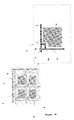
- Fig. 16 shows a section of the prior art TFT display panel (1) in which a number of cells or pixels (2) are equidistantly arranged. These cells consist of a TFT (3) which is connected to a transparent electrode, acting as a drain to the TFT. Via connecting lines (5a) (gate) and (6a) (source) the TFT is connected with row connecting lines (5) and column connecting lines (6) which are arranged orthogonally and in a number equivalent to the number of rows and columns of pixels for the display, respectively, in parallel. The intersections of row lines (6) and column lines (6) are electrically insulated with cross-over patches (7).
- TFT display layout shown in Fig. 1 is to be taken only exemplarily, as other layouts may be possible, and the application is likewise applicable to other kinds of display panels, like plasma panels etc.
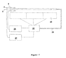
- Fig. 1 is a schematic layout for a display panel according to the invention, using a backlite LCD display as an example.
- a LCD array of panel elements (2) is on each side thereof provided with pixel brightness sensors (8), and incident light sensors (9), respectively (only two of each are depicted) uniformly arranged in both dimensions of the panel at the panel elements (2) of the panel, and are for sensing brightness of the light emitted from the panel elements (2), and luminance of ambient light incident on the panel elements, respectively, at which they are arranged.
- Brightness determining means (25) are connected to the pixel brightness sensors (8) receive input from the sensors (8) and determine brightness differences of the panel elements (2) at which the pixel brightness sensors (8) are arranged.
- Compensation means (26) receive instructions from the determining means (25) and adjust the brightness of panel elements (2) of the display panel, based on the determined brightness differences, in order to compensate brightness inhomogeneities among the panel elements (2). This can be done by regulating the brightness of elements within a backlight (28), or by directly controlling the transmissivity of the LCD elements via control bus (29). Likewise, incident light sensors (9) sensing luminance of ambient light and transmit the information/values to the luminance determining means (27) connected to the incident light sensors (9). This in turn also controls the compensating means (27). The two means (25) and (26) can also be combined, to take account of both values at once.
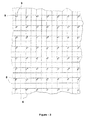
- a first arrangement of the sensors according to the invention is shown.
- Sensors (8) are arranged in intervals along both dimensions of the display panel at a portion of each cell not covered by the transparent electrode (4). Only one kind of sensor is shown, i.e. the first subset of pixel brightness sensors are shown to be uniformly arranged in both dimensions of the panel.
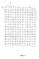
- Fig. 3 shows another arrangement of sensors on a display panel (again exemplified by a TFT panel) according to a further embodiment of the invention, in which both pixel brightness sensors (8) and incident light sensors (9) are arranged at identical panel elements, in order to measure brightness and luminance of and upon the panel display.
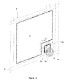
- a particularly preferred embodiment is shown in Fig. 4 , in which both kinds of sensors (8), (9) are arranged at every panel element of a display panel.
- This arrangement allows for a very fine tunable measurement and adjusting of brightness and/or luminance differences.
- no controlling devices for the sensors are shown, though the skilled persons were well aware of the fact that these must be provided.
- a TFT (3) is shown sandwiched between two sensors (8) and (9), in which sensor (8) acts as a pixel brightness sensor sensing light (upward arrows) emitted from a backlight (10), while incident light sensor (9) senses incident light (downward arrows).
- sensor (8) acts as a pixel brightness sensor sensing light (upward arrows) emitted from a backlight (10)
- incident light sensor (9) senses incident light (downward arrows).
- Fig. 5B shows in perspective view a possible arrangement of the two sensors (8) and (9) in relation to the transparent electrode (4). As can be seen, the sensors are arranged in a corner of the transparent electrode, in which also the TFT (3) is arranged.
- pixels or sub-pixels it is also possible to control the colors of pixels or sub-pixels by using this method.
- Each sub-pixel is controlled by independent transistors. So, full color, contrast and brightness control can easily be established by controlling the brightness levels of each sub-pixel.
- Fig. 6 shows such an embodiment in plane view.
- Each sub-pixel (2a, 2b and 2c) contains its own respective sensors (8 (or 9)a, 8b, and 8c).
- diverse processing may be performed in order to obtain desired results. For example, when providing the sub-pixels with luminance sensors below the filters used for generating the respective colors of the panel elements, it will be possible to sense color temperature of a light source the light of which is incident upon the panel display, and to compensate for color temperature of this external light, thereby optimizing the image generated by the display panel. This may be of considerable importance in the field of graphics processing or image manipulation, where precise color preview of an image before printing or publishing is required.
- Fig. 7 shows an embodiment of the present invention with regard to a placement of the sensors on a TFT panel used in this embodiment.
- a circular sensor (8 or 9) is positioned above or below a TFT (3) which is connected to column rows (6) and row lines (5), as explained with regard to Fig. 1 .
- a connecting element (3a) connecting the TFT (3) to the transparent electrode (4).
- sensors may be positioned on both faces of a TFT (3), i.e. above and below the TFT plane of the display panel. This arrangement allows for considerable space saving compared to locating the sensors at a different area of the panel element (2).
- Fig. 9 a layout is shown in which extra wirings are provided for sensors (8, 9) in order to allow for a sensor read out independently of the control signals for the panel elements.
- Pixel brightness sensor (8) is for example on one lead thereof connected with the row connecting line (5) via sensor connecting line (5b), and with another lead connected to pixel brightness sensor line (16) via sensor connecting line (16a).
- Luminance sensor (9) is in turn connected to the row connecting line (5) via a sensor connecting line (5c) and to luminance sensor connecting line (15) via sensor connecting line (15a).
- the TFT is connected to the row connecting line (5) via connecting line (5a), the column connecting lines (6) via connecting lines (6a) and transparent electrode (4) via connecting line (3a). It goes without saying that when using a different basic panel technology; the wiring may quite significantly differ from the wiring presented in Fig. 9 , depending on the technological necessities of the used panel technology and on possibilities for providing the connecting lines.
- Fig. 10 shows a further embodiment of the invention with a somewhat simplified layout in comparison to Fig. 9 .
- the two sensors are connected in series and the panel element contains just one extra wiring per column for connecting both sensors. Accordingly, only one single sensor connecting line (5b) and a single combined sensor connecting line (17a) used to connect the sensors to the combined sensor connecting line (17) is required. While this approach simplifies the layout of connecting lines, additional measures may be required to allow for a timely controlled readout of the sensor information contained in the two sensors (8 and 9).
- FIG. 11 Another preferred embodiment of the present invention is shown in Fig. 11 , in which no additional connection lines are required, and the row lines and column lines (5, 6) are concurrently used by the sensors, additionally to the TFTs.
- a sensor (8) is connected to row connecting line (5) via sensor connecting line (5b) and to column connecting line (6) via sensor connecting line (6b), while sensor (9) is connected to row connecting line (5) via sensor connecting line (5c) and to column connecting line (6) via sensor connecting line (6c).
- a ground connecting line for the electrode (4) which is realized by a ground column connecting line (18), to which the electrode (4) is connected via connecting line (18a) and capacitance (19). Though it may be present in other embodiments, like those of Figs. 9 and 10 , this ground connecting line has been omitted in the other figures.
- Every sensor may be coupled to a charge storage device to store the luminance information. That charge storage device charges or discharges at a rate upon the resistivity or conductivity of the sensor. The charge on the charge storage device provides the luminance information of the effect of environmental light sources on the pixel or backlight luminance level, or both.
- This charge storage device is preferably employed when the approaches shown in Figs. 10 and 11 are used, since in these embodiments, a storage of the sensed information is required, due to the fact that this information can only be transmitted intermittently and concurrently with either the information of the respective other sensor ( Fig. 10 ) or the controlling signals of the TFTs ( Fig. 11 ).
- Fig. 12 shows a further preferred embodiment of the electric layout of the sensors arranged at a panel element (2) of a display panel.
- This embodiment has additional provisions for enabling and disabling the sensors.
- an enable column line (20) is additionally provided, to which the sensors (8, 9) are connected via enable connecting lines (20a, 20b) respectively.
- the sensors are additionally connected in parallel to ground connecting line (18) via connecting line (18b).
- the TFT when the light emitting device is in an emitting state, uses the connections.
- sensors use the connections in order.
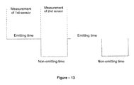
- the sensing may be done at different timings of the emitting panel elements.
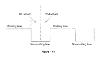
- the measurement of a first sensor for example the pixel brightness sensor (8), may be performed at an emitting time period of the panel element (2), while the measurement of the second sensor, for example the luminance sensor 9, may be performed at a non-emitting time period of the panel element (2).
- connections of the luminance sensors can be similar to TFT driving parts of the pixels / sub-pixels. They can also be connected in parallel / serial to TFT parts. By this way, there will be no need for additional connection lines for the sensors. In this preferred method of the invention, the same connections are used to drive TFT parts and luminance sensors.
- connection lines are used for controlling the panel element(s) connected therewith.
- the sensors (8, 9) use the connections for transmitting stored sensing information, e.g. the charge stored in a charge storage device described above. If two sensors are arranged at a panel element, both may be connected to the connection line und may use it sequentially.
- the situation shown in Fig. 14 corresponds to the measurements in Fig. 13 , i.e. the first sensor, which is used first, must be read out first, while the second sensor can only be read out after its measurement has already started at the non-emitting time period.
- Environmental light sources may have different effects on each pixel. Some panel elements may be perceived dark and some pixels may be perceived bright, because of environmental light sources shining on the respective panel elements.
- a self-driven pixel display device, as disclosed herein, is a solution to have a better perceived view on the display.
- the inventive method is also applicable to adjusting only the backlight or environmental light effects. That means at least one luminance sensor (9) for each pixel / sub-pixel measures a luminance level of the backlight or environmental light source effects on the display panel and a pixel / sub-pixel adjustment is established by using the luminance level data.
- the backlight adjustment procedure is described and shown in Figure 15 below exemplarily for a backlight equipped TFT panel. It is to be understood that this procedure has to be adapted to different panel technologies and may be varied according to necessities of the layout, etc.
- One or more sensors are grouped together to control individual backlight sources (lamps), since the display panel also comprises more than one light source for backlighting the panel elements (S101).
- the luminance values of these grouped sensors are read and/or stored at the same time or sequentially, depending on the configuration of the connection lines and the controller(s) (S102).
- the average backlight luminance value is calculated (S103), stored (S104) and sequentially selected for comparison (S105).
- the general average backlight luminance value for the backlight behind the display panel is also calculated (S111) by taking the average value of the average backlight luminance values of every sensor group or taking the average value of every pixel in groups during reading luminance information from sensors, and the calculated value is stored (S112).
- the average backlight luminance values of the sensors groups are compared with the general average backlight luminance value (S106) selected in step (S105) to check if the average backlight luminance values are within a range of tolerated values of the general average backlight luminance value of the display panel (S107). This tolerated value range is set by the manufacturer or the user.
- the luminance of the backlight source of that sensor group is increased or decreased based upon the difference between the average backlight luminance value of that sensor group (S116) and the general average backlight luminance value of the display panel.
- the value of the increase or decrease in the luminance of the backlight source may be the difference between the average backlight luminance value of that sensor group and the general average backlight luminance value of the display panel, or as set by the manufacturer or the user.
- the adjustment should be repeated and re-controlled after having made changes to the luminance values of the backlight sources.
- a counter for every backlight source or other group S115.
- the counter related with a particular light source is incremented by one for every adjustment made on that backlight source.
- the adjustment procedure can be repeated after decreasing luminance values of every backlight source (S113) when the count of that backlight source reaches a predetermined value.
- backlight brightness uniformity can be established even if there are one or more possibly defunct backlight sources on the display panel.
- the backlight luminance characteristic of the display panel changes with the brightness of the display panel.
- the temperature of the backlight sources changes with the usage time.
- the luminance of a light source takes different values for different temperatures. So, backlight adjustment should be repeated for a predetermined time sequence or when the brightness is changed by the user. Hence, after the backlight adjustment has be completed (S109), the procedure waits for a predetermined time or upon changes to the backlight brightness value (S110), returns to step (S102).
- all of the backlight luminance values of the sensors on the display panel should be sensed to find the minimum pixel backlight value (MPBV) for adjusting individual pixel brightness. Also, all of the backlight luminance values can be stored to have better performance at operations for pixel brightness adjustment.
- MPBV minimum pixel backlight value
- the adjustment of individual pixel brightness is the procedure to calculate the effective pixel picture value (PPVeff).
- Pixel backlight luminance value (PBV) - which is measured by the sensors - of that pixel, the minimum pixel backlight value (MPBV) of the display panel and the pixel picture value (PPV) (the value of the pixel in a video frame) should be known to calculate the effective pixel picture value (PPVeff) for that pixel.
- PPVeff should be calculated for every pixel and for every frame.
- the adjustment formula may change upon the characteristics of display panels.
- PBV can be measured by the related sensor during the pixel brightness adjustment.
- the main purpose of reducing the effects of environmental light sources on the display panel is to increase visibility of the display panel for a user.
- the pixel environmental luminance (PEL) value for every pixel / sub-pixel should be known.
- the luminance sensor on front of the TFT parts of the display panel is used to get the PEL value of the pixel / sub-pixel.
- Environmental light sources have different effects on different PPVs.
- the effect of an environmental light source on a pixel changes with the brightness, contrast and color values of that pixel.
- the effect of the environmental light on a pixel changes with the characteristic of the environmental light. That means; the effect of the environmental light on a pixel changes with its luminance and color.
- the color of the environmental light can be determined as the sensors are behind the color filters of the pixels / sub-pixels. As they are also capable of determining the luminance of the environmental light, the characteristics of the environmental light can be analyzed and be used in adjustment.
- Pixel environmental light (PEL) value of a pixel / sub-pixel is a coefficient for the operation of calculating new brightness, contrast and color values for that pixel / sub-pixel. These new values are used to calculate new pixel picture values for environmental light effects (PPVenv).
- the adjustment for reducing the environmental light effects on the display panel is driving pixels / sub-pixels with their PPVenv.
- the adjustment procedure is repeated for predetermined time sequences.
- This time sequence can be set by the manufacturer or the user.
- the operations for calculating new brightness, contrast and color values for pixels / sub-pixels may change with the structure of the display panel. So, the calculation of new brightness, contrast and color values for reducing environmental light effects on the display panel should be defined by the manufacturer.
- This method may be a part of the production of display panels. So, TV manufacturers do not need to make any changes on their cabinet molds or other mechanical design changes. Only some electronic modification is needed.
- the principle of the inventive method is adjusting pixel / sub-pixel brightness and improving backlight uniformity by using the environmental and backlight luminance information that is determined from luminance sensors placed in every pixel / sub-pixel of the display panel. This method is also a solution for reducing effects of environmental light effects on display panels.
Landscapes
- Engineering & Computer Science (AREA)
- Physics & Mathematics (AREA)
- Computer Hardware Design (AREA)
- General Physics & Mathematics (AREA)
- Theoretical Computer Science (AREA)
- Chemical & Material Sciences (AREA)
- Crystallography & Structural Chemistry (AREA)
- Control Of El Displays (AREA)
- Liquid Crystal Display Device Control (AREA)
- Devices For Indicating Variable Information By Combining Individual Elements (AREA)
- Control Of Indicators Other Than Cathode Ray Tubes (AREA)
Applications Claiming Priority (1)
| Application Number | Priority Date | Filing Date | Title |
|---|---|---|---|
| TR2007/05747A TR200705747A2 (tr) | 2007-08-17 | 2007-08-17 | Ekran panellerinde arka-ışık ve piksel parlaklığının otomatik ayarlanması |
Publications (3)
| Publication Number | Publication Date |
|---|---|
| EP2028640A2 true EP2028640A2 (de) | 2009-02-25 |
| EP2028640A3 EP2028640A3 (de) | 2009-12-16 |
| EP2028640B1 EP2028640B1 (de) | 2013-04-24 |
Family
ID=39929969
Family Applications (1)
| Application Number | Title | Priority Date | Filing Date |
|---|---|---|---|
| EP08160797.0A Active EP2028640B1 (de) | 2007-08-17 | 2008-07-21 | Sich automatisch einstellende Hintergrundbeleuchtung und Pixelhelligkeit auf Anzeigetafeln |
Country Status (3)
| Country | Link |
|---|---|
| EP (1) | EP2028640B1 (de) |
| ES (1) | ES2423015T3 (de) |
| TR (1) | TR200705747A2 (de) |
Cited By (14)
| Publication number | Priority date | Publication date | Assignee | Title |
|---|---|---|---|---|
| US20130215133A1 (en) * | 2012-02-17 | 2013-08-22 | Monotype Imaging Inc. | Adjusting Content Rendering for Environmental Conditions |
| CN103792704A (zh) * | 2014-01-27 | 2014-05-14 | 北京京东方视讯科技有限公司 | 一种测试装置及其方法、显示装置及其显示方法 |
| US9336749B2 (en) | 2010-12-31 | 2016-05-10 | Barco N.V. | Display device and means to measure and isolate the ambient light |
| WO2020062925A1 (zh) * | 2018-09-29 | 2020-04-02 | 京东方科技集团股份有限公司 | 电致发光显示面板及其亮度补偿方法 |
| CN111211149A (zh) * | 2020-01-08 | 2020-05-29 | 武汉华星光电半导体显示技术有限公司 | 显示屏及显示装置 |
| CN111258118A (zh) * | 2020-03-24 | 2020-06-09 | 京东方科技集团股份有限公司 | 显示基板及其控制方法、显示装置 |
| CN111384042A (zh) * | 2018-12-27 | 2020-07-07 | 群创光电股份有限公司 | 电子装置 |
| CN112415754A (zh) * | 2020-12-14 | 2021-02-26 | Oppo广东移动通信有限公司 | 显示面板及其显示装置、头戴显示设备、显示均匀性校准方法 |
| CN112840393A (zh) * | 2018-10-11 | 2021-05-25 | ams有限公司 | 环境光传感器 |
| CN113990267A (zh) * | 2021-11-02 | 2022-01-28 | Tcl华星光电技术有限公司 | 像素的亮度补偿方法、装置、存储介质及显示面板 |
| CN114495859A (zh) * | 2022-02-24 | 2022-05-13 | 深圳创维-Rgb电子有限公司 | 画面显示方法、装置、显示终端以及存储介质 |
| CN115775543A (zh) * | 2022-12-23 | 2023-03-10 | 重庆惠科金渝光电科技有限公司 | 背光模组及显示装置 |
| CN117711300A (zh) * | 2023-06-20 | 2024-03-15 | 荣耀终端有限公司 | 一种图像的显示方法、电子设备、可读存储介质和芯片 |
| CN120692986A (zh) * | 2025-08-21 | 2025-09-23 | 惠科股份有限公司 | 显示面板及其控制方法、显示装置 |
Citations (2)
| Publication number | Priority date | Publication date | Assignee | Title |
|---|---|---|---|---|
| EP1335430A1 (de) | 2002-02-12 | 2003-08-13 | Eastman Kodak Company | Pixel für einen Flachbildschirm mit Luminanz-Rückkopplung |
| US20070115228A1 (en) | 2005-11-18 | 2007-05-24 | Roberts John K | Systems and methods for calibrating solid state lighting panels |
Family Cites Families (7)
| Publication number | Priority date | Publication date | Assignee | Title |
|---|---|---|---|---|
| US5831693A (en) * | 1996-02-22 | 1998-11-03 | Honeywell | Integrated light sensor for an active matrix liquid crystal display panel |
| JP4628770B2 (ja) * | 2004-02-09 | 2011-02-09 | 株式会社日立製作所 | 照明装置を備えた画像表示装置及び画像表示方法 |
| WO2006006537A1 (ja) * | 2004-07-12 | 2006-01-19 | Sony Corporation | バックライトユニットの駆動装置及びその駆動方法 |
| US7636078B2 (en) * | 2005-05-20 | 2009-12-22 | Semiconductor Energy Laboratory Co., Ltd. | Display device and electronic device |
| US7364306B2 (en) * | 2005-06-20 | 2008-04-29 | Digital Display Innovations, Llc | Field sequential light source modulation for a digital display system |
| KR101177579B1 (ko) * | 2005-12-30 | 2012-08-27 | 엘지디스플레이 주식회사 | 액정표시장치 및 그 구동방법 |
| US8791645B2 (en) * | 2006-02-10 | 2014-07-29 | Honeywell International Inc. | Systems and methods for controlling light sources |
-
2007
- 2007-08-17 TR TR2007/05747A patent/TR200705747A2/xx unknown
-
2008
- 2008-07-21 ES ES08160797T patent/ES2423015T3/es active Active
- 2008-07-21 EP EP08160797.0A patent/EP2028640B1/de active Active
Patent Citations (2)
| Publication number | Priority date | Publication date | Assignee | Title |
|---|---|---|---|---|
| EP1335430A1 (de) | 2002-02-12 | 2003-08-13 | Eastman Kodak Company | Pixel für einen Flachbildschirm mit Luminanz-Rückkopplung |
| US20070115228A1 (en) | 2005-11-18 | 2007-05-24 | Roberts John K | Systems and methods for calibrating solid state lighting panels |
Cited By (21)
| Publication number | Priority date | Publication date | Assignee | Title |
|---|---|---|---|---|
| US9336749B2 (en) | 2010-12-31 | 2016-05-10 | Barco N.V. | Display device and means to measure and isolate the ambient light |
| US20130215133A1 (en) * | 2012-02-17 | 2013-08-22 | Monotype Imaging Inc. | Adjusting Content Rendering for Environmental Conditions |
| US9472163B2 (en) * | 2012-02-17 | 2016-10-18 | Monotype Imaging Inc. | Adjusting content rendering for environmental conditions |
| CN103792704A (zh) * | 2014-01-27 | 2014-05-14 | 北京京东方视讯科技有限公司 | 一种测试装置及其方法、显示装置及其显示方法 |
| WO2015109775A1 (zh) * | 2014-01-27 | 2015-07-30 | 京东方科技集团股份有限公司 | 一种测试装置及其方法、显示装置及其显示方法 |
| WO2020062925A1 (zh) * | 2018-09-29 | 2020-04-02 | 京东方科技集团股份有限公司 | 电致发光显示面板及其亮度补偿方法 |
| US11456340B2 (en) | 2018-09-29 | 2022-09-27 | Chengdu Boe Optoelectronics Technology Co., Ltd. | Electroluminescent display panel and brightness compensation method therefor |
| CN112840393A (zh) * | 2018-10-11 | 2021-05-25 | ams有限公司 | 环境光传感器 |
| CN112840393B (zh) * | 2018-10-11 | 2024-10-29 | ams有限公司 | 环境光传感器 |
| CN111384042A (zh) * | 2018-12-27 | 2020-07-07 | 群创光电股份有限公司 | 电子装置 |
| CN111211149A (zh) * | 2020-01-08 | 2020-05-29 | 武汉华星光电半导体显示技术有限公司 | 显示屏及显示装置 |
| CN111258118A (zh) * | 2020-03-24 | 2020-06-09 | 京东方科技集团股份有限公司 | 显示基板及其控制方法、显示装置 |
| US12271077B2 (en) | 2020-03-24 | 2025-04-08 | Boe Technology Group Co., Ltd. | Display substrate, control method thereof, and display device |
| CN112415754A (zh) * | 2020-12-14 | 2021-02-26 | Oppo广东移动通信有限公司 | 显示面板及其显示装置、头戴显示设备、显示均匀性校准方法 |
| CN112415754B (zh) * | 2020-12-14 | 2022-11-11 | Oppo广东移动通信有限公司 | 显示面板及其显示装置、头戴显示设备、显示均匀性校准方法 |
| CN113990267A (zh) * | 2021-11-02 | 2022-01-28 | Tcl华星光电技术有限公司 | 像素的亮度补偿方法、装置、存储介质及显示面板 |
| CN114495859B (zh) * | 2022-02-24 | 2023-07-25 | 深圳创维-Rgb电子有限公司 | 画面显示方法、装置、显示终端以及存储介质 |
| CN114495859A (zh) * | 2022-02-24 | 2022-05-13 | 深圳创维-Rgb电子有限公司 | 画面显示方法、装置、显示终端以及存储介质 |
| CN115775543A (zh) * | 2022-12-23 | 2023-03-10 | 重庆惠科金渝光电科技有限公司 | 背光模组及显示装置 |
| CN117711300A (zh) * | 2023-06-20 | 2024-03-15 | 荣耀终端有限公司 | 一种图像的显示方法、电子设备、可读存储介质和芯片 |
| CN120692986A (zh) * | 2025-08-21 | 2025-09-23 | 惠科股份有限公司 | 显示面板及其控制方法、显示装置 |
Also Published As
| Publication number | Publication date |
|---|---|
| EP2028640A3 (de) | 2009-12-16 |
| ES2423015T3 (es) | 2013-09-17 |
| EP2028640B1 (de) | 2013-04-24 |
| TR200705747A2 (tr) | 2009-03-23 |
Similar Documents
| Publication | Publication Date | Title |
|---|---|---|
| EP2028640B1 (de) | Sich automatisch einstellende Hintergrundbeleuchtung und Pixelhelligkeit auf Anzeigetafeln | |
| RU2467366C1 (ru) | Жидкокристаллическое устройство отображения | |
| US20110109655A1 (en) | Backlight and display device using the same | |
| US8040317B2 (en) | Backlight device having LEDs controlled as a function of target values and influential extent data | |
| US7474294B2 (en) | Use of a plurality of light sensors to regulate a direct-firing backlight for a display | |
| TWI393100B (zh) | Display device and driving method thereof | |
| EP1873578B1 (de) | Oberflächenlichtquellenvorrichtung und Flüssigkristallanzeigeeinheit | |
| US7940013B2 (en) | Lighting apparatus and display apparatus therewith | |
| KR101204865B1 (ko) | 백라이트의 구동 장치, 백라이트 및 이를 구비한액정표시장치 및 백라이트 구동의 방법 | |
| TWI404004B (zh) | 背光模組之驅動裝置及驅動方法 | |
| US20040246435A1 (en) | Liquid crystal display device | |
| CN104913239B (zh) | 面状照明装置及液晶显示装置 | |
| US20090201669A1 (en) | Backlight device, and display apparatus using the same | |
| US20140111560A1 (en) | Liquid crystal display device | |
| US20090058792A1 (en) | Backlight unit, liquid crystal display device including the same, and localized dimming method thereof | |
| EP3063756A1 (de) | Anzeigesystem und verfahren zur herstellung davon | |
| US20120139975A1 (en) | Display Device | |
| KR20120135946A (ko) | 대형 디스플레이 장치 및 그의 휘도 제어 방법 | |
| US20130021349A1 (en) | Display device, liquid crystal module, and image display system | |
| CN100510899C (zh) | 显示装置及其驱动方法 | |
| KR101041354B1 (ko) | 스캐닝 백라이트를 구비한 lcd 패널 | |
| JP4882657B2 (ja) | バックライト制御装置、バックライト制御方法、および液晶表示装置 | |
| CN116741106A (zh) | 补偿显示器驱动参数的方法与电路系统 | |
| US10255842B2 (en) | Displaying system having a function of sensing displaying properties | |
| US8976104B2 (en) | Display device and driving method thereof |
Legal Events
| Date | Code | Title | Description |
|---|---|---|---|
| PUAI | Public reference made under article 153(3) epc to a published international application that has entered the european phase |
Free format text: ORIGINAL CODE: 0009012 |
|
| 17P | Request for examination filed |
Effective date: 20080820 |
|
| AK | Designated contracting states |
Kind code of ref document: A2 Designated state(s): AT BE BG CH CY CZ DE DK EE ES FI FR GB GR HR HU IE IS IT LI LT LU LV MC MT NL NO PL PT RO SE SI SK TR |
|
| AX | Request for extension of the european patent |
Extension state: AL BA MK RS |
|
| PUAL | Search report despatched |
Free format text: ORIGINAL CODE: 0009013 |
|
| AK | Designated contracting states |
Kind code of ref document: A3 Designated state(s): AT BE BG CH CY CZ DE DK EE ES FI FR GB GR HR HU IE IS IT LI LT LU LV MC MT NL NO PL PT RO SE SI SK TR |
|
| AX | Request for extension of the european patent |
Extension state: AL BA MK RS |
|
| AKX | Designation fees paid |
Designated state(s): AT BE BG CH CY CZ DE DK EE ES FI FR GB GR HR HU IE IS IT LI LT LU LV MC MT NL NO PL PT RO SE SI SK TR |
|
| 17Q | First examination report despatched |
Effective date: 20111227 |
|
| RIC1 | Information provided on ipc code assigned before grant |
Ipc: G09G 3/34 20060101AFI20120502BHEP Ipc: G09G 3/36 20060101ALI20120502BHEP |
|
| GRAP | Despatch of communication of intention to grant a patent |
Free format text: ORIGINAL CODE: EPIDOSNIGR1 |
|
| GRAS | Grant fee paid |
Free format text: ORIGINAL CODE: EPIDOSNIGR3 |
|
| GRAP | Despatch of communication of intention to grant a patent |
Free format text: ORIGINAL CODE: EPIDOSNIGR1 |
|
| GRAA | (expected) grant |
Free format text: ORIGINAL CODE: 0009210 |
|
| AK | Designated contracting states |
Kind code of ref document: B1 Designated state(s): AT BE BG CH CY CZ DE DK EE ES FI FR GB GR HR HU IE IS IT LI LT LU LV MC MT NL NO PL PT RO SE SI SK TR |
|
| REG | Reference to a national code |
Ref country code: GB Ref legal event code: FG4D |
|
| REG | Reference to a national code |
Ref country code: CH Ref legal event code: EP |
|
| REG | Reference to a national code |
Ref country code: AT Ref legal event code: REF Ref document number: 609030 Country of ref document: AT Kind code of ref document: T Effective date: 20130515 |
|
| REG | Reference to a national code |
Ref country code: IE Ref legal event code: FG4D |
|
| REG | Reference to a national code |
Ref country code: DE Ref legal event code: R096 Ref document number: 602008024014 Country of ref document: DE Effective date: 20130620 |
|
| REG | Reference to a national code |
Ref country code: AT Ref legal event code: MK05 Ref document number: 609030 Country of ref document: AT Kind code of ref document: T Effective date: 20130424 |
|
| REG | Reference to a national code |
Ref country code: ES Ref legal event code: FG2A Ref document number: 2423015 Country of ref document: ES Kind code of ref document: T3 Effective date: 20130917 |
|
| REG | Reference to a national code |
Ref country code: LT Ref legal event code: MG4D |
|
| REG | Reference to a national code |
Ref country code: NL Ref legal event code: VDEP Effective date: 20130424 |
|
| PG25 | Lapsed in a contracting state [announced via postgrant information from national office to epo] |
Ref country code: LT Free format text: LAPSE BECAUSE OF FAILURE TO SUBMIT A TRANSLATION OF THE DESCRIPTION OR TO PAY THE FEE WITHIN THE PRESCRIBED TIME-LIMIT Effective date: 20130424 Ref country code: SE Free format text: LAPSE BECAUSE OF FAILURE TO SUBMIT A TRANSLATION OF THE DESCRIPTION OR TO PAY THE FEE WITHIN THE PRESCRIBED TIME-LIMIT Effective date: 20130424 Ref country code: GR Free format text: LAPSE BECAUSE OF FAILURE TO SUBMIT A TRANSLATION OF THE DESCRIPTION OR TO PAY THE FEE WITHIN THE PRESCRIBED TIME-LIMIT Effective date: 20130725 Ref country code: BE Free format text: LAPSE BECAUSE OF FAILURE TO SUBMIT A TRANSLATION OF THE DESCRIPTION OR TO PAY THE FEE WITHIN THE PRESCRIBED TIME-LIMIT Effective date: 20130424 Ref country code: SI Free format text: LAPSE BECAUSE OF FAILURE TO SUBMIT A TRANSLATION OF THE DESCRIPTION OR TO PAY THE FEE WITHIN THE PRESCRIBED TIME-LIMIT Effective date: 20130424 Ref country code: NO Free format text: LAPSE BECAUSE OF FAILURE TO SUBMIT A TRANSLATION OF THE DESCRIPTION OR TO PAY THE FEE WITHIN THE PRESCRIBED TIME-LIMIT Effective date: 20130724 Ref country code: AT Free format text: LAPSE BECAUSE OF FAILURE TO SUBMIT A TRANSLATION OF THE DESCRIPTION OR TO PAY THE FEE WITHIN THE PRESCRIBED TIME-LIMIT Effective date: 20130424 Ref country code: FI Free format text: LAPSE BECAUSE OF FAILURE TO SUBMIT A TRANSLATION OF THE DESCRIPTION OR TO PAY THE FEE WITHIN THE PRESCRIBED TIME-LIMIT Effective date: 20130424 Ref country code: IS Free format text: LAPSE BECAUSE OF FAILURE TO SUBMIT A TRANSLATION OF THE DESCRIPTION OR TO PAY THE FEE WITHIN THE PRESCRIBED TIME-LIMIT Effective date: 20130824 Ref country code: PT Free format text: LAPSE BECAUSE OF FAILURE TO SUBMIT A TRANSLATION OF THE DESCRIPTION OR TO PAY THE FEE WITHIN THE PRESCRIBED TIME-LIMIT Effective date: 20130826 |
|
| PG25 | Lapsed in a contracting state [announced via postgrant information from national office to epo] |
Ref country code: HR Free format text: LAPSE BECAUSE OF FAILURE TO SUBMIT A TRANSLATION OF THE DESCRIPTION OR TO PAY THE FEE WITHIN THE PRESCRIBED TIME-LIMIT Effective date: 20130424 Ref country code: BG Free format text: LAPSE BECAUSE OF FAILURE TO SUBMIT A TRANSLATION OF THE DESCRIPTION OR TO PAY THE FEE WITHIN THE PRESCRIBED TIME-LIMIT Effective date: 20130724 Ref country code: PL Free format text: LAPSE BECAUSE OF FAILURE TO SUBMIT A TRANSLATION OF THE DESCRIPTION OR TO PAY THE FEE WITHIN THE PRESCRIBED TIME-LIMIT Effective date: 20130424 Ref country code: LV Free format text: LAPSE BECAUSE OF FAILURE TO SUBMIT A TRANSLATION OF THE DESCRIPTION OR TO PAY THE FEE WITHIN THE PRESCRIBED TIME-LIMIT Effective date: 20130424 Ref country code: CY Free format text: LAPSE BECAUSE OF FAILURE TO SUBMIT A TRANSLATION OF THE DESCRIPTION OR TO PAY THE FEE WITHIN THE PRESCRIBED TIME-LIMIT Effective date: 20130424 |
|
| PG25 | Lapsed in a contracting state [announced via postgrant information from national office to epo] |
Ref country code: SK Free format text: LAPSE BECAUSE OF FAILURE TO SUBMIT A TRANSLATION OF THE DESCRIPTION OR TO PAY THE FEE WITHIN THE PRESCRIBED TIME-LIMIT Effective date: 20130424 Ref country code: DK Free format text: LAPSE BECAUSE OF FAILURE TO SUBMIT A TRANSLATION OF THE DESCRIPTION OR TO PAY THE FEE WITHIN THE PRESCRIBED TIME-LIMIT Effective date: 20130424 Ref country code: CZ Free format text: LAPSE BECAUSE OF FAILURE TO SUBMIT A TRANSLATION OF THE DESCRIPTION OR TO PAY THE FEE WITHIN THE PRESCRIBED TIME-LIMIT Effective date: 20130424 Ref country code: EE Free format text: LAPSE BECAUSE OF FAILURE TO SUBMIT A TRANSLATION OF THE DESCRIPTION OR TO PAY THE FEE WITHIN THE PRESCRIBED TIME-LIMIT Effective date: 20130424 |
|
| PG25 | Lapsed in a contracting state [announced via postgrant information from national office to epo] |
Ref country code: MC Free format text: LAPSE BECAUSE OF FAILURE TO SUBMIT A TRANSLATION OF THE DESCRIPTION OR TO PAY THE FEE WITHIN THE PRESCRIBED TIME-LIMIT Effective date: 20130424 Ref country code: RO Free format text: LAPSE BECAUSE OF FAILURE TO SUBMIT A TRANSLATION OF THE DESCRIPTION OR TO PAY THE FEE WITHIN THE PRESCRIBED TIME-LIMIT Effective date: 20130424 Ref country code: NL Free format text: LAPSE BECAUSE OF FAILURE TO SUBMIT A TRANSLATION OF THE DESCRIPTION OR TO PAY THE FEE WITHIN THE PRESCRIBED TIME-LIMIT Effective date: 20130424 |
|
| PLBE | No opposition filed within time limit |
Free format text: ORIGINAL CODE: 0009261 |
|
| REG | Reference to a national code |
Ref country code: CH Ref legal event code: PL |
|
| STAA | Information on the status of an ep patent application or granted ep patent |
Free format text: STATUS: NO OPPOSITION FILED WITHIN TIME LIMIT |
|
| 26N | No opposition filed |
Effective date: 20140127 |
|
| REG | Reference to a national code |
Ref country code: IE Ref legal event code: MM4A |
|
| PG25 | Lapsed in a contracting state [announced via postgrant information from national office to epo] |
Ref country code: CH Free format text: LAPSE BECAUSE OF NON-PAYMENT OF DUE FEES Effective date: 20130731 Ref country code: LI Free format text: LAPSE BECAUSE OF NON-PAYMENT OF DUE FEES Effective date: 20130731 |
|
| REG | Reference to a national code |
Ref country code: DE Ref legal event code: R097 Ref document number: 602008024014 Country of ref document: DE Effective date: 20140127 |
|
| PG25 | Lapsed in a contracting state [announced via postgrant information from national office to epo] |
Ref country code: IE Free format text: LAPSE BECAUSE OF NON-PAYMENT OF DUE FEES Effective date: 20130721 |
|
| REG | Reference to a national code |
Ref country code: FR Ref legal event code: PLFP Year of fee payment: 8 |
|
| PG25 | Lapsed in a contracting state [announced via postgrant information from national office to epo] |
Ref country code: MT Free format text: LAPSE BECAUSE OF FAILURE TO SUBMIT A TRANSLATION OF THE DESCRIPTION OR TO PAY THE FEE WITHIN THE PRESCRIBED TIME-LIMIT Effective date: 20130424 |
|
| PG25 | Lapsed in a contracting state [announced via postgrant information from national office to epo] |
Ref country code: LU Free format text: LAPSE BECAUSE OF NON-PAYMENT OF DUE FEES Effective date: 20130721 Ref country code: HU Free format text: LAPSE BECAUSE OF FAILURE TO SUBMIT A TRANSLATION OF THE DESCRIPTION OR TO PAY THE FEE WITHIN THE PRESCRIBED TIME-LIMIT; INVALID AB INITIO Effective date: 20080721 |
|
| REG | Reference to a national code |
Ref country code: FR Ref legal event code: PLFP Year of fee payment: 9 |
|
| REG | Reference to a national code |
Ref country code: FR Ref legal event code: PLFP Year of fee payment: 10 |
|
| REG | Reference to a national code |
Ref country code: FR Ref legal event code: PLFP Year of fee payment: 11 |
|
| PGFP | Annual fee paid to national office [announced via postgrant information from national office to epo] |
Ref country code: ES Payment date: 20200922 Year of fee payment: 13 Ref country code: FR Payment date: 20200722 Year of fee payment: 13 Ref country code: TR Payment date: 20200717 Year of fee payment: 13 Ref country code: DE Payment date: 20200721 Year of fee payment: 13 Ref country code: GB Payment date: 20200727 Year of fee payment: 13 |
|
| PGFP | Annual fee paid to national office [announced via postgrant information from national office to epo] |
Ref country code: IT Payment date: 20200724 Year of fee payment: 13 |
|
| REG | Reference to a national code |
Ref country code: DE Ref legal event code: R119 Ref document number: 602008024014 Country of ref document: DE |
|
| GBPC | Gb: european patent ceased through non-payment of renewal fee |
Effective date: 20210721 |
|
| PG25 | Lapsed in a contracting state [announced via postgrant information from national office to epo] |
Ref country code: GB Free format text: LAPSE BECAUSE OF NON-PAYMENT OF DUE FEES Effective date: 20210721 Ref country code: DE Free format text: LAPSE BECAUSE OF NON-PAYMENT OF DUE FEES Effective date: 20220201 |
|
| PG25 | Lapsed in a contracting state [announced via postgrant information from national office to epo] |
Ref country code: FR Free format text: LAPSE BECAUSE OF NON-PAYMENT OF DUE FEES Effective date: 20210731 |
|
| PG25 | Lapsed in a contracting state [announced via postgrant information from national office to epo] |
Ref country code: IT Free format text: LAPSE BECAUSE OF NON-PAYMENT OF DUE FEES Effective date: 20210721 |
|
| REG | Reference to a national code |
Ref country code: ES Ref legal event code: FD2A Effective date: 20220927 |
|
| PG25 | Lapsed in a contracting state [announced via postgrant information from national office to epo] |
Ref country code: ES Free format text: LAPSE BECAUSE OF NON-PAYMENT OF DUE FEES Effective date: 20210722 |