EP2024994B1 - Method to prevent metal contamination by a substrate holder - Google Patents
Method to prevent metal contamination by a substrate holder Download PDFInfo
- Publication number
- EP2024994B1 EP2024994B1 EP07729748.9A EP07729748A EP2024994B1 EP 2024994 B1 EP2024994 B1 EP 2024994B1 EP 07729748 A EP07729748 A EP 07729748A EP 2024994 B1 EP2024994 B1 EP 2024994B1
- Authority
- EP
- European Patent Office
- Prior art keywords
- substrate
- based coating
- carbon based
- group
- coating
- Prior art date
- Legal status (The legal status is an assumption and is not a legal conclusion. Google has not performed a legal analysis and makes no representation as to the accuracy of the status listed.)
- Active
Links
Images
Classifications
-
- C—CHEMISTRY; METALLURGY
- C23—COATING METALLIC MATERIAL; COATING MATERIAL WITH METALLIC MATERIAL; CHEMICAL SURFACE TREATMENT; DIFFUSION TREATMENT OF METALLIC MATERIAL; COATING BY VACUUM EVAPORATION, BY SPUTTERING, BY ION IMPLANTATION OR BY CHEMICAL VAPOUR DEPOSITION, IN GENERAL; INHIBITING CORROSION OF METALLIC MATERIAL OR INCRUSTATION IN GENERAL
- C23C—COATING METALLIC MATERIAL; COATING MATERIAL WITH METALLIC MATERIAL; SURFACE TREATMENT OF METALLIC MATERIAL BY DIFFUSION INTO THE SURFACE, BY CHEMICAL CONVERSION OR SUBSTITUTION; COATING BY VACUUM EVAPORATION, BY SPUTTERING, BY ION IMPLANTATION OR BY CHEMICAL VAPOUR DEPOSITION, IN GENERAL
- C23C14/00—Coating by vacuum evaporation, by sputtering or by ion implantation of the coating forming material
- C23C14/06—Coating by vacuum evaporation, by sputtering or by ion implantation of the coating forming material characterised by the coating material
- C23C14/0605—Carbon
-
- C—CHEMISTRY; METALLURGY
- C23—COATING METALLIC MATERIAL; COATING MATERIAL WITH METALLIC MATERIAL; CHEMICAL SURFACE TREATMENT; DIFFUSION TREATMENT OF METALLIC MATERIAL; COATING BY VACUUM EVAPORATION, BY SPUTTERING, BY ION IMPLANTATION OR BY CHEMICAL VAPOUR DEPOSITION, IN GENERAL; INHIBITING CORROSION OF METALLIC MATERIAL OR INCRUSTATION IN GENERAL
- C23C—COATING METALLIC MATERIAL; COATING MATERIAL WITH METALLIC MATERIAL; SURFACE TREATMENT OF METALLIC MATERIAL BY DIFFUSION INTO THE SURFACE, BY CHEMICAL CONVERSION OR SUBSTITUTION; COATING BY VACUUM EVAPORATION, BY SPUTTERING, BY ION IMPLANTATION OR BY CHEMICAL VAPOUR DEPOSITION, IN GENERAL
- C23C16/00—Chemical coating by decomposition of gaseous compounds, without leaving reaction products of surface material in the coating, i.e. chemical vapour deposition [CVD] processes
- C23C16/22—Chemical coating by decomposition of gaseous compounds, without leaving reaction products of surface material in the coating, i.e. chemical vapour deposition [CVD] processes characterised by the deposition of inorganic material, other than metallic material
- C23C16/26—Deposition of carbon only
-
- H—ELECTRICITY
- H10—SEMICONDUCTOR DEVICES; ELECTRIC SOLID-STATE DEVICES NOT OTHERWISE PROVIDED FOR
- H10P—GENERIC PROCESSES OR APPARATUS FOR THE MANUFACTURE OR TREATMENT OF DEVICES COVERED BY CLASS H10
- H10P72/00—Handling or holding of wafers, substrates or devices during manufacture or treatment thereof
- H10P72/70—Handling or holding of wafers, substrates or devices during manufacture or treatment thereof for supporting or gripping
- H10P72/76—Handling or holding of wafers, substrates or devices during manufacture or treatment thereof for supporting or gripping using mechanical means, e.g. clamps or pinches
- H10P72/7604—Handling or holding of wafers, substrates or devices during manufacture or treatment thereof for supporting or gripping using mechanical means, e.g. clamps or pinches the wafers being placed on a susceptor, stage or support
- H10P72/7616—Handling or holding of wafers, substrates or devices during manufacture or treatment thereof for supporting or gripping using mechanical means, e.g. clamps or pinches the wafers being placed on a susceptor, stage or support characterised by a coating, a hardness or a material
-
- Y—GENERAL TAGGING OF NEW TECHNOLOGICAL DEVELOPMENTS; GENERAL TAGGING OF CROSS-SECTIONAL TECHNOLOGIES SPANNING OVER SEVERAL SECTIONS OF THE IPC; TECHNICAL SUBJECTS COVERED BY FORMER USPC CROSS-REFERENCE ART COLLECTIONS [XRACs] AND DIGESTS
- Y10—TECHNICAL SUBJECTS COVERED BY FORMER USPC
- Y10T—TECHNICAL SUBJECTS COVERED BY FORMER US CLASSIFICATION
- Y10T428/00—Stock material or miscellaneous articles
- Y10T428/30—Self-sustaining carbon mass or layer with impregnant or other layer
Definitions
- the invention relates to a method to provide a substrate with a conductive, metal free, hydrophilic carbon based coating and to a substrate provided with such a coating.
- Carbon based coatings such as diamond-like carbon coatings or diamond-like nanocomposite coatings are known in the art.
- carbon based coatings need to be conductive. It is generally known to dope a carbon based coating with a metal such as a transition metal to influence the electrical conductivity of the coating.
- components coated with carbon based coatings are for example components to transport and/or support semiconductor substrates such as electrostatic chucks, wafer carriers, lift pins and heaters.
- the carbon based coating is generally doped with a metal such as a transition metal.
- Preferred doping elements known in the art of carbon based coatings are Fe, Cr, Ni, Co, Ti, W, Zn, Cu, Mn, Al, Na, Ca and K.
- possible metal contamination is a big concern as metal contamination on a semiconductor substrate may degrade the electrical properties of a semiconductor substrate. As features and linewidths on microprocessors are getting smaller and smaller, the risk of metal contamination is becoming higher.
- VOCs volatile organic compounds
- a substrate a method to increase the wettability of a substrate as well as a method to allow cleaning of a substrate with deionized water is provided.
- the method comprises providing the substrate at least partially with a conductive, metal free, hydrophilic carbon based coating, wherein the substrate is selected from the group consisting of components to transport and/or support a semiconductor substrate, such as electrostatic chucks, wafer carriers, heaters, lift pins and components to transport and/or support highly purity liquids, copier components and components used in Electrical Discharge Machining (EDM) applications,
- the carbon based coating is doped with nitrogen and the carbon based coating has an electrical resistivity lower than 10 8 ohm-cm.
- an adhesion promoting layer is applied on said substrate (10, 20) before the application of said carbon based coating (13), wherein the adhesion promoting layer comprises one or more layers of a carbide, a nitride, a carbonitride, an oxycarbide, an oxynitride, an oxycarbonitride of a metal selected from the group consisting of the elements of group IVB, the elements of group VB and the elements of group VIB of the periodic table.
- the coating according to the present invention is metal free. This is important for applications whereby metal contamination is an issue.
- a great advantage of the present invention is that the coating layer is at the same time conductive, metal free and hydrophilic.
- the coating according to the present invention is in particular suitable for substrates whereby metal contamination is an issue.
- Such substrates comprise for example components to transport and/or support a semiconductor substrate.
- Examples of such components comprise electrostatics chucks, wafer carriers, heaters and lift pins.
- semiconductor substrates include semiconductor wafers. Components to transport and/or support a semiconductor substrate require a slightly conductive coating that avoids any possible contamination of the semiconductor substrate.
- the coating is of particular interest as coating for components to transport and/or support a semiconductor substrate.
- the metal free conductive carbon based coating is applied at least on the surface or surfaces of the component that come in contact with the semiconductor substrate.
- the metal free conductive carbon based coating can be applied on other surfaces of the component as well.
- the whole outer surface of the component is covered with a metal free conductive carbon based coating.
- the coating is also suitable to coat components to transport and/or support high purity liquids used in semiconductor patterning and lithography.
- the coating according to the present invention is suitable for substrates requiring a slightly conductive coating for charge dissipation.
- substrates comprise copier components such as donor rolls, or for components used in Electrical Discharge Machining (EDM) applications.
- EDM Electrical Discharge Machining
- the electrical resistivity of the carbon based coating is preferably lower than 10 8 ohm-cm, for example between 10 3 ohm-cm and 10 8 ohm-cm and more preferably between 10 4 ohm-cm and 10 6 ohm-cm.
- the concentration of nitrogen is preferably between 0.1 and 20 at% and more preferably between 3 and 7 at%.
- the coating has a low coefficient of friction.
- a coating with a low coefficient of friction is preferred to reduce the formation and deposition of friction or abrasion resulting particles on the semiconductor substrate.
- the coefficient of friction of the coating is lower than 0.15 as for example between 0.05 and 0.10.
- the coating has a high hardness for example to avoid scratching and abrasion.
- the hardness of the coating is higher than 10 GPa, for example higher than 12 GPa, 15 GPa , 18 GPa , 20 GPa or 25 GPa .
- the carbon based coating has preferably a thickness ranging between 0.5 ⁇ m and 10 ⁇ m, and more preferably between 2.5 ⁇ m and 8 ⁇ m.
- Preferred carbon based layers comprise diamond-like carbon (DLC) coatings and diamond-like nanocomposite (DLN) coatings.
- DLC diamond-like carbon
- DLN diamond-like nanocomposite
- Diamond-like carbon (DLC) coatings comprise amorphous hydrogenated carbon (a-C:H).
- DLC coatings comprise a mixture of sp 2 and sp 3 bonded carbon with a hydrogen concentration between 0 and 80 % and preferably between 20 and 30 %.
- the hardness of a DLC layer is preferably between 15 GPa and 25 GPa. More preferably, the hardness of a DLC layer is between 18 GPa and 25 GPa.
- Diamond like nanocomposite (DLN) coatings comprise an amorphous structure of C, H, Si and O. Diamond like nanocomposite coatings are commercially known as DYLYN ® coatings.
- the hardness of a diamond layer nanocomposite layer is preferably between 10 GPa and 20 GPa.
- a DLN coating comprises in proportion to the sum of C, Si, and O : 40 to 90 at% C, 5 to 40 at% Si, and 5 to 25 at% O.
- the diamond-like nanocomposite composition comprises two interpenetrating networks of a-C:H and a-Si:O.
- the carbon based coating can be deposited by any technique known in the art.
- Preferred deposition techniques comprise ion beam deposition, pulsed laser deposition, arc deposition, such as filtered or non-filtered arc deposition, chemical vapor deposition, such as enhanced plasma assisted chemical vapor deposition and laser arc deposition.
- the adhesion promoting layer comprises more than one layer, for example two or more metal layers, each layer comprising a metal selected from the group consisting of silicon, the elements of group IVB, the elements of group VB and the elements of group VIB of the periodic table, as for example a Ti or Cr layer.
- the adhesion promoting layer comprises one or more layers of a carbide, a nitride, a carbonitride, an oxycarbide, an oxynitride, an oxycarbonitride of a metal selected from the group consisting of silicon, the elements of group IVB, the elements of group VB and the elements of group VIB of the periodic table.
- a carbide a nitride, a carbonitride, an oxycarbide, an oxynitride, an oxycarbonitride of a metal selected from the group consisting of silicon, the elements of group IVB, the elements of group VB and the elements of group VIB of the periodic table.
- Some examples are TiN, CrN, TiC, Cr 2 C 3 , TiCN and CrCN.
- the adhesion promoting layer may comprise any combination of one or more metal layers of a metal selected from the group consisting of the elements of group IVB, the elements of group VB and the elements of group VIB of the periodic table and one or more layers of a carbide, a nitride, a carbonitride, an oxycarbide, an oxynitride, an oxycarbonitride of a metal selected from the group consisting of silicon, the elements of group IVB, the elements of group VB and the elements of group VIB of the periodic table.
- Some examples of intermediate layers comprise the combination of a metal layer and a metal carbide layer, the combination of a metal layer and a metal nitride layer, the combination of a metal layer and a metal carbonitride layer, the combination of a first metal layer, a metal carbide layer and a second metal layer and the combination of a first metal layer, a metal nitride layer and a second metal layer.
- the thickness of the adhesion promoting layer is preferably between 1 nm and 1000 nm, as for example between 10 and 500 nm.
- the adhesion promoting layer can be deposited by any technique known in the art as for example physical vapor deposition, such as sputtering or evaporation.
- the electrical resistivity is between 10 3 ohm-cm and 10 8 ohm-cm and more preferably between 10° ohm-cm and 10 6 ohm-cm.
- a method to allow cleaning of a substrate (10, 20) with deionized water which substrate (10, 20) is selected from the group consisting of components to transport and/or support a semiconductor substrate, such as electrostatic chucks, wafer carriers, heaters, lift pins and components to transport and/or support highly purity liquids, copier components and components used in Electrical Discharge Machining (EDM) applications, said method comprising the steps ofproviding a substrate (10, 20), said substrate (10, 20) being at least partially coated with a conductive, metal free, hydrophilic carbon based coating (13), said carbon based coating (13) being doped with nitrogen and having an electrical resistivity lower than 10 8 ohm-cm;
- the wettability of the substrate is increased as the surface is more hydrophilic. Consequently, it is possible to clean the surface by using deioinzed water.
- Electrostatic chucks are widely used to retain substrates, such as semiconductor wafers or other workpieces, in a stationary position during processing.
- electrostatic chucks typically contain one or more electrodes superimposed on or embedded in a dielectric material. As power is applied to the electrode, an attractive force is generated between the electrostatic chuck and the substrate disposed thereon.
- the electrostatic chuck may be required to coat the electrostatic chuck with a coating layer having some conductivity so that the particle generation between the surface of the electrostatic chuck and the wafer is minimal.
- the conductivity of the coating helps also to maintain the substrate at the desired process condition with minimal process deviation.
- the electrostatic chuck 10 comprises
- the metal free conductive carbon based coating 13 according to the present invention has a thickness ranging from 1 to 10 ⁇ m and is preferably between 3 and 7 ⁇ m.
- the coating has an electrical resistivity ranging between 10 3 ohm-cm and 10 8 ohm-cm, and more preferably between 10 4 ohm-cm and 10 6 ohm-cm.
- the coating comprises between 50 and 70 at% C, between 20 and 30 at% H and between 3 and 7 at% N.
- the coating 13 has a hardness in the range of 15 to 19 GPa.
- the metal free conductive carbon based coating can be applied on the whole surface of the dielectric body 12 coming into contact with the substrate or can be applied on the dielectric body 12 in a pattern.
- This pattern is preferably optimized to provide an optimal electrostatic chucking force and wafer supporting area with minimal particle generation.
- Figure 2 shows a lift pin 20 according to the present invention.
- the lift pin 20 comprises a member 21 having a tip 22 adapted to lift and lower a substrate 24.
- the lift pin 20 is coated at least at the tip 22 with a metal free conductive carbon based coating 23.
- the metal free conductive carbon based coating 24 according to the present invention has a thickness ranging between 1 and 10 ⁇ m and preferably ranging between 2 and 4 ⁇ m.
- the coating has an electrical resistivity ranging from 10 3 ohm-cm to 10 8 ohm-cm and more preferably between 10 4 ohm-cm and 10 6 ohm-cm.
- the coating comprises between 50 and 70 at% C, between 20 and 30 at% H and between 3 and 7 at% N.
- the coating 23 has a hardness in the range of 15 to 19 GPa.
Landscapes
- Chemical & Material Sciences (AREA)
- Chemical Kinetics & Catalysis (AREA)
- Engineering & Computer Science (AREA)
- Materials Engineering (AREA)
- Mechanical Engineering (AREA)
- Metallurgy (AREA)
- Organic Chemistry (AREA)
- Inorganic Chemistry (AREA)
- General Chemical & Material Sciences (AREA)
- Container, Conveyance, Adherence, Positioning, Of Wafer (AREA)
- Physical Vapour Deposition (AREA)
- Carbon And Carbon Compounds (AREA)
Description
- The invention relates to a method to provide a substrate with a conductive, metal free, hydrophilic carbon based coating and to a substrate provided with such a coating.
- Carbon based coatings such as diamond-like carbon coatings or diamond-like nanocomposite coatings are known in the art.
- Respective prior art can be found for example in
WO 01/90016 A -
WO 2005/083752 A2 ,US - A - 5 812 362 , Cheah L K et al. (Journal of non-crystalline solids, North-Holland publishing company, Amsterdam, NI, vol. 242, no. 1, 1 December 1998 (1998 12-01), pages 40 - 48, or Robertson J et al. (Diamond and related materials, Elsevier Science Publishers, Amsterdam, NI, vol. 4, no. 4, 15 April 1995 (1995-04-15), pages 441-4444). - For many applications carbon based coatings need to be conductive. It is generally known to dope a carbon based coating with a metal such as a transition metal to influence the electrical conductivity of the coating.
- Examples of components coated with carbon based coatings are for example components to transport and/or support semiconductor substrates such as electrostatic chucks, wafer carriers, lift pins and heaters.
- In some microchip manufacturing processes, these components require an electrically conductive coating and therefore the carbon based coating is generally doped with a metal such as a transition metal. Preferred doping elements known in the art of carbon based coatings are Fe, Cr, Ni, Co, Ti, W, Zn, Cu, Mn, Al, Na, Ca and K. However, especially for semiconductor applications, possible metal contamination is a big concern as metal contamination on a semiconductor substrate may degrade the electrical properties of a semiconductor substrate. As features and linewidths on microprocessors are getting smaller and smaller, the risk of metal contamination is becoming higher.
- The presence of metallic parts or metal dopants in the system that might come in contact with the wafer can be sufficient to cause metal contamination.
- Even the simple phenomenon of sliding a wafer on a metallic surface and/or on a metal containing surface is enough to contaminate the wafer.
- Elements such as Na, K and Cu are completely unacceptable currently. Other elements such as Al and Ti are tolerated for the current generation of semiconductor processes. However, processes which will
- Elements such as Na, K and Cu are completely unacceptable currently. Other elements such as Al and Ti are tolerated for the current generation of semiconductor processes. However, processes which will be used for 45 nm nodes or lower nodes will not tolerate any kind of metal contamination.
- Therefore, it is desirable to prevent any possible contamination.
- To avoid microcontamination surfaces have to be cleaned regularly. Generally, the cleaning is done with organic solvents. However as there is an increasing concern about the use of volatile organic compounds (VOCs) one is looking for alternative cleaning process. Consequently, there is a high interest in cleaning processes using non volatile components.
- Since diamond like carbon coatings are generally hydrophobic, wettability is an issue for these applications.
- It is an object of the present invention to avoid the problems of the prior art.
- It is another object to provide a method to provide a substrate with a conductive coating that is metal free so that metal contamination is avoided.
- It is a further object of the present invention to provide a method to increase the wettability of a component so that this component can be cleaned with deionized water.
- It is still a further object of the present invention to provide a substrate with a wear resistant, hard, low friction, thermal stable, conductive, metal free conductive carbon based coating.
- According to the present invention, a substrate a method to increase the wettability of a substrate as well as a method to allow cleaning of a substrate with deionized water is provided.
- The method comprises providing the substrate at least partially with a conductive, metal free, hydrophilic carbon based coating, wherein the substrate is selected from the group consisting of components to transport and/or support a semiconductor substrate, such as electrostatic chucks, wafer carriers, heaters, lift pins and components to transport and/or support highly purity liquids, copier components and components used in Electrical Discharge Machining (EDM) applications, The carbon based coating is doped with nitrogen and the carbon based coating has an electrical resistivity lower than 108 ohm-cm. According to the invention, an adhesion promoting layer is applied on said substrate (10, 20) before the application of said carbon based coating (13), wherein the adhesion promoting layer comprises one or more layers of a carbide, a nitride, a carbonitride, an oxycarbide, an oxynitride, an oxycarbonitride of a metal selected from the group consisting of the elements of group IVB, the elements of group VB and the elements of group VIB of the periodic table.
- By applying a conductive, metal free coating comprising nitrogen the wettability of the substrate is increased as the surface is more hydrophilic. Consequently, the surface of the coated substrate can be cleaned more easily. As the surface is more hydrophilic deioinzed water can be used to clean the surface and the use of VOCs can be avoided. Furthermore, the coating according to the present invention is metal free. This is important for applications whereby metal contamination is an issue.
- A great advantage of the present invention is that the coating layer is at the same time conductive, metal free and hydrophilic.
- The coating according to the present invention is in particular suitable for substrates whereby metal contamination is an issue.
- Such substrates comprise for example components to transport and/or support a semiconductor substrate.
- Examples of such components comprise electrostatics chucks, wafer carriers, heaters and lift pins.
- Examples of semiconductor substrates include semiconductor wafers. Components to transport and/or support a semiconductor substrate require a slightly conductive coating that avoids any possible contamination of the semiconductor substrate.
- As the coating according to the present invention meets these requirements, the coating is of particular interest as coating for components to transport and/or support a semiconductor substrate. The metal free conductive carbon based coating is applied at least on the surface or surfaces of the component that come in contact with the semiconductor substrate.
- Possibly, the metal free conductive carbon based coating can be applied on other surfaces of the component as well.
- In some embodiments the whole outer surface of the component is covered with a metal free conductive carbon based coating.
- The coating is also suitable to coat components to transport and/or support high purity liquids used in semiconductor patterning and lithography.
- Furthermore, the coating according to the present invention is suitable for substrates requiring a slightly conductive coating for charge dissipation. Examples of such substrates comprise copier components such as donor rolls, or for components used in Electrical Discharge Machining (EDM) applications.
- The electrical resistivity of the carbon based coating is preferably lower than 108 ohm-cm, for example between 103 ohm-cm and 108 ohm-cm and more preferably between 104 ohm-cm and 106 ohm-cm.
- The concentration of nitrogen is preferably between 0.1 and 20 at% and more preferably between 3 and 7 at%.
- For most applications, it is preferred that the coating has a low coefficient of friction. For semiconductor applications a coating with a low coefficient of friction is preferred to reduce the formation and deposition of friction or abrasion resulting particles on the semiconductor substrate.
- Preferably, the coefficient of friction of the coating is lower than 0.15 as for example between 0.05 and 0.10.
- Furthermore, for most applications, it is preferred that the coating has a high hardness for example to avoid scratching and abrasion. Preferably, the hardness of the coating is higher than 10 GPa, for example higher than 12 GPa, 15 GPa , 18 GPa , 20 GPa or 25 GPa .
- The carbon based coating has preferably a thickness ranging between 0.5 µm and 10 µm, and more preferably between 2.5 µm and 8 µm.
- Any type of carbon based layer can be considered. Preferred carbon based layers comprise diamond-like carbon (DLC) coatings and diamond-like nanocomposite (DLN) coatings.
- Diamond-like carbon (DLC) coatings comprise amorphous hydrogenated carbon (a-C:H). DLC coatings comprise a mixture of sp2 and sp3 bonded carbon with a hydrogen concentration between 0 and 80 % and preferably between 20 and 30 %.
- The hardness of a DLC layer is preferably between 15 GPa and 25 GPa. More preferably, the hardness of a DLC layer is between 18 GPa and 25 GPa.
- Diamond like nanocomposite (DLN) coatings comprise an amorphous structure of C, H, Si and O. Diamond like nanocomposite coatings are commercially known as DYLYN® coatings.
- The hardness of a diamond layer nanocomposite layer is preferably between 10 GPa and 20 GPa.
- Preferably, a DLN coating comprises in proportion to the sum of C, Si, and O : 40 to 90 at% C, 5 to 40 at% Si, and 5 to 25 at% O.
- Preferably, the diamond-like nanocomposite composition comprises two interpenetrating networks of a-C:H and a-Si:O.
- The carbon based coating can be deposited by any technique known in the art.
- Preferred deposition techniques comprise ion beam deposition, pulsed laser deposition, arc deposition, such as filtered or non-filtered arc deposition, chemical vapor deposition, such as enhanced plasma assisted chemical vapor deposition and laser arc deposition.
- Possibly, the adhesion promoting layer comprises more than one layer, for example two or more metal layers, each layer comprising a metal selected from the group consisting of silicon, the elements of group IVB, the elements of group VB and the elements of group VIB of the periodic table, as for example a Ti or Cr layer.
- According to the invention, the adhesion promoting layer comprises one or more layers of a carbide, a nitride, a carbonitride, an oxycarbide, an oxynitride, an oxycarbonitride of a metal selected from the group consisting of silicon, the elements of group IVB, the elements of group VB and the elements of group VIB of the periodic table. Some examples are TiN, CrN, TiC, Cr2C3, TiCN and CrCN.
- Furthermore, the adhesion promoting layer may comprise any combination of one or more metal layers of a metal selected from the group consisting of the elements of group IVB, the elements of group VB and the elements of group VIB of the periodic table and one or more layers of a carbide, a nitride, a carbonitride, an oxycarbide, an oxynitride, an oxycarbonitride of a metal selected from the group consisting of silicon, the elements of group IVB, the elements of group VB and the elements of group VIB of the periodic table.
- Some examples of intermediate layers comprise the combination of a metal layer and a metal carbide layer, the combination of a metal layer and a metal nitride layer, the combination of a metal layer and a metal carbonitride layer, the combination of a first metal layer, a metal carbide layer and a second metal layer and the combination of a first metal layer, a metal nitride layer and a second metal layer.
- The thickness of the adhesion promoting layer is preferably between 1 nm and 1000 nm, as for example between 10 and 500 nm.
- The adhesion promoting layer can be deposited by any technique known in the art as for example physical vapor deposition, such as sputtering or evaporation.
- According to a second aspect of the present invention a substrate (10, 20) selected from the group consisting of components to transport and/or support a semiconductor substrate, such as electrostatic chucks, wafer carriers, heaters, lift pins and components to transport and/or support highly purity liquids, copier components and components used in Electrical Discharge Machining (EDM) applications, being coated at least partially with a conductive, metal free, hydrophilic carbon based coating (13), said metal free conductive carbon based coating (13) being doped with nitrogen, said carbon based coating having an electrical resistivity lower than 108 ohm-cm, wherein an adhesion promoting layer is applied on said substrate (10, 20) before the application of said carbon based coating (13), wherein the adhesion promoting layer comprises one or more layers of a carbide, a nitride, a carbonitride, an oxycarbide, an oxynitride, an oxycarbonitride of a metal selected from the group consisting of the elements of group IVB, the elements of group VB and the elements of group VIB of the periodic table.
- Preferably, the electrical resistivity is between 103 ohm-cm and 108 ohm-cm and more preferably between 10° ohm-cm and 106 ohm-cm. According to a third aspect of the present invention a method to allow cleaning of a substrate (10, 20) with deionized water, which substrate (10, 20) is selected from the group consisting of components to transport and/or support a semiconductor substrate, such as electrostatic chucks, wafer carriers, heaters, lift pins and components to transport and/or support highly purity liquids, copier components and components used in Electrical Discharge Machining (EDM) applications, said method comprising the steps ofproviding a substrate (10, 20), said substrate (10, 20) being at least partially coated with a conductive, metal free, hydrophilic carbon based coating (13), said carbon based coating (13) being doped with nitrogen and having an electrical resistivity lower than 108 ohm-cm;
- cleaning said substrate (10, 20) with deionized water, wherein an adhesion promoting layer is applied on said substrate (10, 20) before the application of said carbon based coating (13), wherein the adhesion promoting layer comprises one or more layers of a carbide, a nitride, a carbonitride, an oxycarbide, an oxynitride, an oxycarbonitride of a metal selected from the group consisting of the elements of group IVB, the elements of
group VB and the elements of group VIB of the periodic table. The cleaning may comprise rinsing and/or wiping and/or any other method of cleaning. - By applying a coating according to the present invention, the the wettability of the substrate is increased as the surface is more hydrophilic. Consequently, it is possible to clean the surface by using deioinzed water.
- The invention will now be described into more detail with reference to the accompanying drawings wherein
-
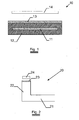
Figure 1 is a cross-sectional view of an electrostatic chuck according to the present invention; -
Figure 2 is a cross-sectional view of an assembly comprising a lift pin according to the present invention. - A preferred embodiment of an
electrostatic chuck 10 according to the present invention is described with reference toFigure 1 . Electrostatic chucks are widely used to retain substrates, such as semiconductor wafers or other workpieces, in a stationary position during processing. - Typically, electrostatic chucks contain one or more electrodes superimposed on or embedded in a dielectric material. As power is applied to the electrode, an attractive force is generated between the electrostatic chuck and the substrate disposed thereon.
- It may be required to coat the electrostatic chuck with a coating layer having some conductivity so that the particle generation between the surface of the electrostatic chuck and the wafer is minimal.
- The conductivity of the coating helps also to maintain the substrate at the desired process condition with minimal process deviation.
- However, any possible metal contamination should be avoided.
- A preferred embodiment of an
electrostatic chuck 10 according to the present invention is described with reference toFigure 1 . - The
electrostatic chuck 10 comprises - at least one
electrode 11; - a dielectric body 12 at least partially covering the
electrode 11; - a metal free conductive carbon based
coating 13 at least partially covering the dielectric body 12. - As power is applied to the electrode, an attractive force is generated between the electrostatic chuck and the
substrate 14 disposed thereon. - The metal free conductive carbon based
coating 13 according to the present invention has a thickness ranging from 1 to 10 µm and is preferably between 3 and 7 µm. The coating has an electrical resistivity ranging between 103 ohm-cm and 108 ohm-cm, and more preferably between 104 ohm-cm and 106 ohm-cm. - The coating comprises between 50 and 70 at% C, between 20 and 30 at% H and between 3 and 7 at% N. The
coating 13 has a hardness in the range of 15 to 19 GPa. - The metal free conductive carbon based coating can be applied on the whole surface of the dielectric body 12 coming into contact with the substrate or can be applied on the dielectric body 12 in a pattern.
- This pattern is preferably optimized to provide an optimal electrostatic chucking force and wafer supporting area with minimal particle generation.
-
Figure 2 shows alift pin 20 according to the present invention. - The
lift pin 20 comprises amember 21 having atip 22 adapted to lift and lower asubstrate 24. - The
lift pin 20 is coated at least at thetip 22 with a metal free conductive carbon basedcoating 23. - The metal free conductive carbon based
coating 24 according to the present invention has a thickness ranging between 1 and 10 µm and preferably ranging between 2 and 4 µm. The coating has an electrical resistivity ranging from 103 ohm-cm to 108 ohm-cm and more preferably between 104 ohm-cm and 106 ohm-cm. - The coating comprises between 50 and 70 at% C, between 20 and 30 at% H and between 3 and 7 at% N. The
coating 23 has a hardness in the range of 15 to 19 GPa.
Claims (11)
- A method to increase the wettability of a substrate (10, 20), which substrate (10, 20) is selected from the group consisting of components to transport and/or support a semiconductor substrate, such as electrostatic chucks, wafer carriers, heaters, lift pins and components to transport and/or support highly purity liquids, copier components and components used in Electrical Discharge Machining (EDM) applications, by providing said substrate (10, 20) at least partially with a conductive, metal free, hydrophilic carbon based coating (13), said carbon based coating (13) being doped with nitrogen, said carbon based coating (13) having an electrical resistivity lower than 108 ohm-cm, characterized in that an adhesion promoting layer is applied on said substrate (10, 20) before the application of said carbon based coating (13), wherein the adhesion promoting layer comprises one or more layers of a carbide, a nitride, a carbonitride, an oxycarbide, an oxynitride, an oxycarbonitride of a metal selected from the group consisting of the elements of group IVB, the elements of group VB and
the elements of group VIB of the periodic table. - A method according to claim 1, whereby said carbon based coating (13) comprises between 0.1 and 20 at% nitrogen.
- A method according to any one of the preceding claims, whereby said carbon based coating (13) comprises a nitrogen doped diamond-like carbon (DLC) coating comprising amorphous hydrogenated carbon (a-C:H).
- A method according to any one of claims 1 or 2, whereby said carbon based coating (13) comprises a nitrogen doped diamond-like nanocomposite (DLN) coating comprising C, H, O and Si.
- A method according to claim 4, whereby said diamond-like nanocomposite coating comprises two interpenetrating networks, a first network of predominantly sp3 bonded carbon in a diamond-like carbon network stabilized by hydrogen and a second network of silicon stabilized oxygen.
- A substrate (10, 20) selected from the group consisting of components to transport and/or support a semiconductor substrate, such as electrostatic chucks, wafer carriers, heaters, lift pins and components to transport and/or support highly purity liquids, copier components and components used in Electrical Discharge Machining (EDM) applications, being coated at least partially with a conductive, metal free, hydrophilic carbon based coating (13), said metal free conductive carbon based coating (13) being doped with nitrogen, said carbon based coating having an electrical resistivity lower than 108 ohm-cm, characterized in that an adhesion promoting layer is applied on said substrate (10, 20) before the application of said carbon based coating (13), wherein the adhesion promoting layer comprises one or more layers of a carbide, a nitride, a carbonitride, an oxycarbide, an oxynitride, an oxycarbonitride of a metal selected from the group consisting of the elements of group IVB, the elements of group VB and the elements of group VIB of the periodic table.
- A substrate (10, 20) according to claim 6 whereby said carbon based coating (13) comprises between 0.1 and 20 at% nitrogen.
- A substrate (10, 20) according to any one of claims 6 or 7, whereby said carbon based coating (13) comprises a nitrogen doped diamond-like carbon (DLC) coating comprising amorphous hydrogenated carbon (a-C:H).
- A substrate (10, 20) according to any one of claims 6 or 7, whereby said carbon based coating (13) comprises a nitrogen doped diamond-like nanocomposite (DLN) coating comprising C, H, O and Si.
- A substrate (10, 20) according to claim 9, whereby said diamond-like nanocomposite coating comprises two interpenetrating networks, a first network of predominantly sp3 bonded carbon in a diamond-like carbon network stabilized by hydrogen and a second network of silicon stabilized oxygen.
- A method to allow cleaning of a substrate (10, 20) with deionized water, which substrate (10, 20) is selected from the group consisting of components to transport and/or support a semiconductor substrate, such as electrostatic chucks, wafer carriers, heaters, lift pins and components to transport and/or support highly purity liquids, copier components and components used in Electrical Discharge Machining (EDM) applications, said method comprising the steps of- providing a substrate (10, 20), said substrate (10, 20) being at least partially coated with a conductive, metal free, hydrophilic carbon based coating (13), said carbon based coating (13) being doped with nitrogen and having an electrical resistivity lower than 108 ohm-cm;- cleaning said substrate (10, 20) with deionized water, characterized in that an adhesion promoting layer is applied on said substrate (10, 20) before the application of said carbon based coating (13), wherein the adhesion promoting layer comprises one or more layers of a carbide, a nitride, a carbonitride, an oxycarbide, an oxynitride, an oxycarbonitride of a metal selected from the group consisting of the elements of group IVB, the elements of group VB and the elements of group VIB of the periodic table.
Priority Applications (2)
| Application Number | Priority Date | Filing Date | Title |
|---|---|---|---|
| EP07729748.9A EP2024994B1 (en) | 2006-06-02 | 2007-05-31 | Method to prevent metal contamination by a substrate holder |
| EP14165494.7A EP2763162B1 (en) | 2006-06-02 | 2007-05-31 | Preventing metal contamination of a component in semi-conductors |
Applications Claiming Priority (3)
| Application Number | Priority Date | Filing Date | Title |
|---|---|---|---|
| EP06114915 | 2006-06-02 | ||
| EP07729748.9A EP2024994B1 (en) | 2006-06-02 | 2007-05-31 | Method to prevent metal contamination by a substrate holder |
| PCT/EP2007/055346 WO2007141191A1 (en) | 2006-06-02 | 2007-05-31 | Method to prevent metal contamination by a substrate holder |
Related Child Applications (1)
| Application Number | Title | Priority Date | Filing Date |
|---|---|---|---|
| EP14165494.7A Division EP2763162B1 (en) | 2006-06-02 | 2007-05-31 | Preventing metal contamination of a component in semi-conductors |
Publications (2)
| Publication Number | Publication Date |
|---|---|
| EP2024994A1 EP2024994A1 (en) | 2009-02-18 |
| EP2024994B1 true EP2024994B1 (en) | 2014-04-23 |
Family
ID=37414318
Family Applications (2)
| Application Number | Title | Priority Date | Filing Date |
|---|---|---|---|
| EP07729748.9A Active EP2024994B1 (en) | 2006-06-02 | 2007-05-31 | Method to prevent metal contamination by a substrate holder |
| EP14165494.7A Active EP2763162B1 (en) | 2006-06-02 | 2007-05-31 | Preventing metal contamination of a component in semi-conductors |
Family Applications After (1)
| Application Number | Title | Priority Date | Filing Date |
|---|---|---|---|
| EP14165494.7A Active EP2763162B1 (en) | 2006-06-02 | 2007-05-31 | Preventing metal contamination of a component in semi-conductors |
Country Status (5)
| Country | Link |
|---|---|
| US (2) | US20090142599A1 (en) |
| EP (2) | EP2024994B1 (en) |
| JP (1) | JP5289307B2 (en) |
| CN (1) | CN101467243B (en) |
| WO (1) | WO2007141191A1 (en) |
Families Citing this family (7)
| Publication number | Priority date | Publication date | Assignee | Title |
|---|---|---|---|---|
| TWI534940B (en) * | 2010-09-08 | 2016-05-21 | 恩特格林斯公司 | High conductivity electrostatic chuck |
| US20150062772A1 (en) * | 2013-08-27 | 2015-03-05 | Varian Semiconductor Equipment Associates, Inc | Barrier Layer For Electrostatic Chucks |
| US10261121B2 (en) * | 2016-05-26 | 2019-04-16 | Intel Corporation | Diamond-like carbon coated semiconductor equipment |
| JP7012454B2 (en) * | 2017-04-27 | 2022-01-28 | 株式会社岡本工作機械製作所 | Manufacturing method of electrostatic suction chuck and manufacturing method of semiconductor device |
| CN113529031B (en) * | 2020-04-13 | 2023-09-08 | 季华实验室 | Diamond-like film and preparation method |
| DE102022211252A1 (en) | 2021-10-27 | 2023-04-27 | Canon Kabushiki Kaisha | Substrate holding plate, manufacturing method of an apparatus and exposure apparatus |
| JP7528314B2 (en) * | 2022-06-23 | 2024-08-05 | キヤノン株式会社 | Substrate holding plate, substrate holding plate manufacturing method, exposure method and exposure apparatus |
Citations (1)
| Publication number | Priority date | Publication date | Assignee | Title |
|---|---|---|---|---|
| US6228471B1 (en) * | 1997-02-04 | 2001-05-08 | N.V. Bekaert S.A. | Coating comprising layers of diamond like carbon and diamond like nanocomposite compositions |
Family Cites Families (19)
| Publication number | Priority date | Publication date | Assignee | Title |
|---|---|---|---|---|
| KR100189970B1 (en) * | 1995-08-07 | 1999-06-01 | 윤종용 | A polishing apparatus for semiconductor wafer |
| US5746954A (en) * | 1995-09-07 | 1998-05-05 | The Dow Chemical Company | Processes for forming thin, durable coatings of perfluorocarbon ionomers on various substrate materials |
| US5812362A (en) * | 1996-06-14 | 1998-09-22 | Applied Materials, Inc. | Method and apparatus for the use of diamond films as dielectric coatings on electrostatic chucks |
| US5783243A (en) * | 1996-06-24 | 1998-07-21 | Benado; Adam L. | Process for extracting and desolventizing natural oil-containing food products with minimum structural damage |
| KR100274934B1 (en) * | 1997-12-29 | 2001-01-15 | 윤종용 | Semiconductor wafer boat |
| US6303225B1 (en) * | 2000-05-24 | 2001-10-16 | Guardian Industries Corporation | Hydrophilic coating including DLC on substrate |
| JP2001338878A (en) * | 2000-03-21 | 2001-12-07 | Sharp Corp | Susceptor and surface treatment method |
| US6713179B2 (en) * | 2000-05-24 | 2004-03-30 | Guardian Industries Corp. | Hydrophilic DLC on substrate with UV exposure |
| TW517265B (en) * | 2000-06-23 | 2003-01-11 | Applied Materials Inc | Apparatus for supporting a substrate and method of fabricating same |
| US6678143B2 (en) * | 2000-12-11 | 2004-01-13 | General Electric Company | Electrostatic chuck and method of manufacturing the same |
| US6633497B2 (en) * | 2001-06-22 | 2003-10-14 | Hewlett-Packard Development Company, L.P. | Resistive cross point array of short-tolerant memory cells |
| JP3370318B2 (en) * | 2001-07-30 | 2003-01-27 | 株式会社半導体エネルギー研究所 | Member provided with diamond-like carbon film |
| JP2003346317A (en) * | 2002-05-23 | 2003-12-05 | Fuji Photo Film Co Ltd | Perpendicular magnetic recording medium |
| US20050014882A1 (en) * | 2003-05-02 | 2005-01-20 | Brungardt Clement Linus | Aqueous systems containing additive pre-mixes and processes for forming the same |
| JP2005012111A (en) * | 2003-06-20 | 2005-01-13 | Tdk Corp | Magnetoresistance effect element and thin film magnetic head |
| US6862211B2 (en) * | 2003-07-07 | 2005-03-01 | Hewlett-Packard Development Company | Magneto-resistive memory device |
| US6929349B2 (en) * | 2003-10-14 | 2005-08-16 | Lexmark International, Inc. | Thin film ink jet printhead adhesion enhancement |
| JP4247535B2 (en) * | 2003-11-11 | 2009-04-02 | Hoya株式会社 | Magnetic disk for load / unload system, method for manufacturing magnetic disk for load / unload system, and method for evaluating magnetic disk for load / unload system |
| US7824498B2 (en) * | 2004-02-24 | 2010-11-02 | Applied Materials, Inc. | Coating for reducing contamination of substrates during processing |
-
2007
- 2007-05-31 CN CN2007800203926A patent/CN101467243B/en active Active
- 2007-05-31 WO PCT/EP2007/055346 patent/WO2007141191A1/en not_active Ceased
- 2007-05-31 JP JP2009512605A patent/JP5289307B2/en active Active
- 2007-05-31 EP EP07729748.9A patent/EP2024994B1/en active Active
- 2007-05-31 EP EP14165494.7A patent/EP2763162B1/en active Active
- 2007-05-31 US US12/302,133 patent/US20090142599A1/en not_active Abandoned
-
2019
- 2019-09-23 US US16/579,043 patent/US20200017952A1/en not_active Abandoned
Patent Citations (1)
| Publication number | Priority date | Publication date | Assignee | Title |
|---|---|---|---|---|
| US6228471B1 (en) * | 1997-02-04 | 2001-05-08 | N.V. Bekaert S.A. | Coating comprising layers of diamond like carbon and diamond like nanocomposite compositions |
Also Published As
| Publication number | Publication date |
|---|---|
| CN101467243B (en) | 2012-08-08 |
| US20090142599A1 (en) | 2009-06-04 |
| US20200017952A1 (en) | 2020-01-16 |
| WO2007141191A1 (en) | 2007-12-13 |
| CN101467243A (en) | 2009-06-24 |
| EP2763162B1 (en) | 2016-05-11 |
| JP2009539240A (en) | 2009-11-12 |
| EP2024994A1 (en) | 2009-02-18 |
| JP5289307B2 (en) | 2013-09-11 |
| EP2763162A1 (en) | 2014-08-06 |
Similar Documents
| Publication | Publication Date | Title |
|---|---|---|
| US20200017952A1 (en) | Method to prevent metal contamination by a substrate holder | |
| CN100564031C (en) | The object that diamond-like carbon hard multilayer film forms and its manufacture method | |
| US7983017B2 (en) | Electrostatic chuck and method of forming | |
| JP7499406B2 (en) | Electrostatic chuck having embossments containing diamond-like carbon and deposited silicon-based materials and related methods - Patents.com | |
| JP3336682B2 (en) | Hard carbon film | |
| WO2003068503A1 (en) | Novel friction and wear-resistant coatings for tools, dies and microelectromechanical systems | |
| CN101026119A (en) | Etch resistant wafer processing apparatus and method for producing the same | |
| US6080445A (en) | Method of forming films over insulating material | |
| US20030047283A1 (en) | Apparatus for supporting a substrate and method of fabricating same | |
| US12500109B2 (en) | Electrostatic chuck that includes upper ceramic layer that includes a dielectric layer, and related methods and structures | |
| WO2008082977A2 (en) | Electrostatic chuck and method of forming | |
| CN110023052B (en) | Die for processing metal material and method for manufacturing same | |
| WO2004086826A2 (en) | Esd dissipative structural components | |
| US20070274021A1 (en) | Electrostatic chuck apparatus | |
| CN210261965U (en) | Coated tools | |
| CN114075667A (en) | High hardness low friction coefficient protective coating | |
| KR102917126B1 (en) | Antistatic Device | |
| JP3618032B2 (en) | Electrostatic chuck | |
| CN115433901A (en) | antistatic coating | |
| US20260144005A1 (en) | Surface structure of an electrostatic chuck and method for forming the same | |
| CN223885618U (en) | Surface structure of electrostatic chuck | |
| KR20250139498A (en) | Anti-static film and preparation method thereof | |
| KR20180102572A (en) | Absence of wit | |
| KR20180102571A (en) | Absence of wit | |
| JPH11145267A (en) | Substrate storage container and substrate processing method |
Legal Events
| Date | Code | Title | Description |
|---|---|---|---|
| PUAI | Public reference made under article 153(3) epc to a published international application that has entered the european phase |
Free format text: ORIGINAL CODE: 0009012 |
|
| 17P | Request for examination filed |
Effective date: 20081120 |
|
| AK | Designated contracting states |
Kind code of ref document: A1 Designated state(s): AT BE BG CH CY CZ DE DK EE ES FI FR GB GR HU IE IS IT LI LT LU LV MC MT NL PL PT RO SE SI SK TR |
|
| AX | Request for extension of the european patent |
Extension state: AL BA HR MK RS |
|
| RIN1 | Information on inventor provided before grant (corrected) |
Inventor name: VENKATRAMAN, CHANDRA Inventor name: KIRK, MATTHEW P. Inventor name: ACKERMAN, CYNDI, L. Inventor name: DEKEMPENEER, ERIK Inventor name: GROENEN, ROLAND |
|
| 17Q | First examination report despatched |
Effective date: 20101015 |
|
| RAP1 | Party data changed (applicant data changed or rights of an application transferred) |
Owner name: SULZER METAPLAS GMBH |
|
| DAX | Request for extension of the european patent (deleted) | ||
| REG | Reference to a national code |
Ref country code: DE Ref legal event code: R079 Ref document number: 602007036236 Country of ref document: DE Free format text: PREVIOUS MAIN CLASS: H01L0021683000 Ipc: H01L0021687000 |
|
| RIC1 | Information provided on ipc code assigned before grant |
Ipc: C23C 14/06 20060101ALI20130927BHEP Ipc: C23C 16/26 20060101ALI20130927BHEP Ipc: H01L 21/687 20060101AFI20130927BHEP |
|
| GRAP | Despatch of communication of intention to grant a patent |
Free format text: ORIGINAL CODE: EPIDOSNIGR1 |
|
| INTG | Intention to grant announced |
Effective date: 20131115 |
|
| GRAS | Grant fee paid |
Free format text: ORIGINAL CODE: EPIDOSNIGR3 |
|
| GRAA | (expected) grant |
Free format text: ORIGINAL CODE: 0009210 |
|
| AK | Designated contracting states |
Kind code of ref document: B1 Designated state(s): AT BE BG CH CY CZ DE DK EE ES FI FR GB GR HU IE IS IT LI LT LU LV MC MT NL PL PT RO SE SI SK TR |
|
| REG | Reference to a national code |
Ref country code: GB Ref legal event code: FG4D |
|
| REG | Reference to a national code |
Ref country code: CH Ref legal event code: EP |
|
| REG | Reference to a national code |
Ref country code: AT Ref legal event code: REF Ref document number: 664269 Country of ref document: AT Kind code of ref document: T Effective date: 20140515 |
|
| REG | Reference to a national code |
Ref country code: IE Ref legal event code: FG4D |
|
| REG | Reference to a national code |
Ref country code: DE Ref legal event code: R096 Ref document number: 602007036236 Country of ref document: DE Effective date: 20140605 |
|
| REG | Reference to a national code |
Ref country code: NL Ref legal event code: T3 |
|
| REG | Reference to a national code |
Ref country code: LT Ref legal event code: MG4D |
|
| PG25 | Lapsed in a contracting state [announced via postgrant information from national office to epo] |
Ref country code: FI Free format text: LAPSE BECAUSE OF FAILURE TO SUBMIT A TRANSLATION OF THE DESCRIPTION OR TO PAY THE FEE WITHIN THE PRESCRIBED TIME-LIMIT Effective date: 20140423 Ref country code: CY Free format text: LAPSE BECAUSE OF FAILURE TO SUBMIT A TRANSLATION OF THE DESCRIPTION OR TO PAY THE FEE WITHIN THE PRESCRIBED TIME-LIMIT Effective date: 20140423 Ref country code: IS Free format text: LAPSE BECAUSE OF FAILURE TO SUBMIT A TRANSLATION OF THE DESCRIPTION OR TO PAY THE FEE WITHIN THE PRESCRIBED TIME-LIMIT Effective date: 20140823 Ref country code: BG Free format text: LAPSE BECAUSE OF FAILURE TO SUBMIT A TRANSLATION OF THE DESCRIPTION OR TO PAY THE FEE WITHIN THE PRESCRIBED TIME-LIMIT Effective date: 20140723 Ref country code: LT Free format text: LAPSE BECAUSE OF FAILURE TO SUBMIT A TRANSLATION OF THE DESCRIPTION OR TO PAY THE FEE WITHIN THE PRESCRIBED TIME-LIMIT Effective date: 20140423 Ref country code: GR Free format text: LAPSE BECAUSE OF FAILURE TO SUBMIT A TRANSLATION OF THE DESCRIPTION OR TO PAY THE FEE WITHIN THE PRESCRIBED TIME-LIMIT Effective date: 20140724 |
|
| PG25 | Lapsed in a contracting state [announced via postgrant information from national office to epo] |
Ref country code: PL Free format text: LAPSE BECAUSE OF FAILURE TO SUBMIT A TRANSLATION OF THE DESCRIPTION OR TO PAY THE FEE WITHIN THE PRESCRIBED TIME-LIMIT Effective date: 20140423 Ref country code: SE Free format text: LAPSE BECAUSE OF FAILURE TO SUBMIT A TRANSLATION OF THE DESCRIPTION OR TO PAY THE FEE WITHIN THE PRESCRIBED TIME-LIMIT Effective date: 20140423 Ref country code: LV Free format text: LAPSE BECAUSE OF FAILURE TO SUBMIT A TRANSLATION OF THE DESCRIPTION OR TO PAY THE FEE WITHIN THE PRESCRIBED TIME-LIMIT Effective date: 20140423 Ref country code: ES Free format text: LAPSE BECAUSE OF FAILURE TO SUBMIT A TRANSLATION OF THE DESCRIPTION OR TO PAY THE FEE WITHIN THE PRESCRIBED TIME-LIMIT Effective date: 20140423 |
|
| PG25 | Lapsed in a contracting state [announced via postgrant information from national office to epo] |
Ref country code: PT Free format text: LAPSE BECAUSE OF FAILURE TO SUBMIT A TRANSLATION OF THE DESCRIPTION OR TO PAY THE FEE WITHIN THE PRESCRIBED TIME-LIMIT Effective date: 20140825 |
|
| REG | Reference to a national code |
Ref country code: CH Ref legal event code: PL |
|
| REG | Reference to a national code |
Ref country code: DE Ref legal event code: R097 Ref document number: 602007036236 Country of ref document: DE |
|
| PG25 | Lapsed in a contracting state [announced via postgrant information from national office to epo] |
Ref country code: RO Free format text: LAPSE BECAUSE OF FAILURE TO SUBMIT A TRANSLATION OF THE DESCRIPTION OR TO PAY THE FEE WITHIN THE PRESCRIBED TIME-LIMIT Effective date: 20140423 Ref country code: CH Free format text: LAPSE BECAUSE OF NON-PAYMENT OF DUE FEES Effective date: 20140531 Ref country code: LI Free format text: LAPSE BECAUSE OF NON-PAYMENT OF DUE FEES Effective date: 20140531 Ref country code: SK Free format text: LAPSE BECAUSE OF FAILURE TO SUBMIT A TRANSLATION OF THE DESCRIPTION OR TO PAY THE FEE WITHIN THE PRESCRIBED TIME-LIMIT Effective date: 20140423 Ref country code: MC Free format text: LAPSE BECAUSE OF FAILURE TO SUBMIT A TRANSLATION OF THE DESCRIPTION OR TO PAY THE FEE WITHIN THE PRESCRIBED TIME-LIMIT Effective date: 20140423 Ref country code: EE Free format text: LAPSE BECAUSE OF FAILURE TO SUBMIT A TRANSLATION OF THE DESCRIPTION OR TO PAY THE FEE WITHIN THE PRESCRIBED TIME-LIMIT Effective date: 20140423 Ref country code: DK Free format text: LAPSE BECAUSE OF FAILURE TO SUBMIT A TRANSLATION OF THE DESCRIPTION OR TO PAY THE FEE WITHIN THE PRESCRIBED TIME-LIMIT Effective date: 20140423 Ref country code: BE Free format text: LAPSE BECAUSE OF FAILURE TO SUBMIT A TRANSLATION OF THE DESCRIPTION OR TO PAY THE FEE WITHIN THE PRESCRIBED TIME-LIMIT Effective date: 20140423 Ref country code: CZ Free format text: LAPSE BECAUSE OF FAILURE TO SUBMIT A TRANSLATION OF THE DESCRIPTION OR TO PAY THE FEE WITHIN THE PRESCRIBED TIME-LIMIT Effective date: 20140423 |
|
| PLBE | No opposition filed within time limit |
Free format text: ORIGINAL CODE: 0009261 |
|
| STAA | Information on the status of an ep patent application or granted ep patent |
Free format text: STATUS: NO OPPOSITION FILED WITHIN TIME LIMIT |
|
| 26N | No opposition filed |
Effective date: 20150126 |
|
| REG | Reference to a national code |
Ref country code: DE Ref legal event code: R097 Ref document number: 602007036236 Country of ref document: DE Effective date: 20150126 |
|
| PG25 | Lapsed in a contracting state [announced via postgrant information from national office to epo] |
Ref country code: SI Free format text: LAPSE BECAUSE OF FAILURE TO SUBMIT A TRANSLATION OF THE DESCRIPTION OR TO PAY THE FEE WITHIN THE PRESCRIBED TIME-LIMIT Effective date: 20140423 |
|
| PG25 | Lapsed in a contracting state [announced via postgrant information from national office to epo] |
Ref country code: MT Free format text: LAPSE BECAUSE OF FAILURE TO SUBMIT A TRANSLATION OF THE DESCRIPTION OR TO PAY THE FEE WITHIN THE PRESCRIBED TIME-LIMIT Effective date: 20140423 |
|
| REG | Reference to a national code |
Ref country code: FR Ref legal event code: PLFP Year of fee payment: 10 |
|
| PG25 | Lapsed in a contracting state [announced via postgrant information from national office to epo] |
Ref country code: HU Free format text: LAPSE BECAUSE OF FAILURE TO SUBMIT A TRANSLATION OF THE DESCRIPTION OR TO PAY THE FEE WITHIN THE PRESCRIBED TIME-LIMIT; INVALID AB INITIO Effective date: 20070531 Ref country code: LU Free format text: LAPSE BECAUSE OF NON-PAYMENT OF DUE FEES Effective date: 20140531 Ref country code: TR Free format text: LAPSE BECAUSE OF FAILURE TO SUBMIT A TRANSLATION OF THE DESCRIPTION OR TO PAY THE FEE WITHIN THE PRESCRIBED TIME-LIMIT Effective date: 20140423 |
|
| REG | Reference to a national code |
Ref country code: FR Ref legal event code: PLFP Year of fee payment: 11 |
|
| REG | Reference to a national code |
Ref country code: FR Ref legal event code: PLFP Year of fee payment: 12 |
|
| PGFP | Annual fee paid to national office [announced via postgrant information from national office to epo] |
Ref country code: IT Payment date: 20200601 Year of fee payment: 14 Ref country code: GB Payment date: 20200601 Year of fee payment: 14 |
|
| PGFP | Annual fee paid to national office [announced via postgrant information from national office to epo] |
Ref country code: AT Payment date: 20200603 Year of fee payment: 14 |
|
| REG | Reference to a national code |
Ref country code: AT Ref legal event code: MM01 Ref document number: 664269 Country of ref document: AT Kind code of ref document: T Effective date: 20210531 |
|
| GBPC | Gb: european patent ceased through non-payment of renewal fee |
Effective date: 20210531 |
|
| PG25 | Lapsed in a contracting state [announced via postgrant information from national office to epo] |
Ref country code: AT Free format text: LAPSE BECAUSE OF NON-PAYMENT OF DUE FEES Effective date: 20210531 |
|
| PG25 | Lapsed in a contracting state [announced via postgrant information from national office to epo] |
Ref country code: GB Free format text: LAPSE BECAUSE OF NON-PAYMENT OF DUE FEES Effective date: 20210531 |
|
| PG25 | Lapsed in a contracting state [announced via postgrant information from national office to epo] |
Ref country code: IT Free format text: LAPSE BECAUSE OF NON-PAYMENT OF DUE FEES Effective date: 20200531 |
|
| PGFP | Annual fee paid to national office [announced via postgrant information from national office to epo] |
Ref country code: NL Payment date: 20250526 Year of fee payment: 19 |
|
| PGFP | Annual fee paid to national office [announced via postgrant information from national office to epo] |
Ref country code: DE Payment date: 20250528 Year of fee payment: 19 |
|
| PGFP | Annual fee paid to national office [announced via postgrant information from national office to epo] |
Ref country code: FR Payment date: 20250526 Year of fee payment: 19 |
|
| PGFP | Annual fee paid to national office [announced via postgrant information from national office to epo] |
Ref country code: IE Payment date: 20250520 Year of fee payment: 19 |
|
| REG | Reference to a national code |
Ref country code: DE Ref legal event code: R079 Ref document number: 602007036236 Country of ref document: DE Free format text: PREVIOUS MAIN CLASS: H01L0021687000 Ipc: H10P0072760000 |