EP2023397A1 - Light transmitting/receiving device - Google Patents
Light transmitting/receiving device Download PDFInfo
- Publication number
- EP2023397A1 EP2023397A1 EP07743386A EP07743386A EP2023397A1 EP 2023397 A1 EP2023397 A1 EP 2023397A1 EP 07743386 A EP07743386 A EP 07743386A EP 07743386 A EP07743386 A EP 07743386A EP 2023397 A1 EP2023397 A1 EP 2023397A1
- Authority
- EP
- European Patent Office
- Prior art keywords
- light
- groove
- front surface
- receiving device
- light blocking
- Prior art date
- Legal status (The legal status is an assumption and is not a legal conclusion. Google has not performed a legal analysis and makes no representation as to the accuracy of the status listed.)
- Granted
Links
Images


Classifications
-
- G—PHYSICS
- G02—OPTICS
- G02B—OPTICAL ELEMENTS, SYSTEMS OR APPARATUS
- G02B6/00—Light guides; Structural details of arrangements comprising light guides and other optical elements, e.g. couplings
- G02B6/24—Coupling light guides
- G02B6/42—Coupling light guides with opto-electronic elements
- G02B6/4201—Packages, e.g. shape, construction, internal or external details
-
- H—ELECTRICITY
- H01—ELECTRIC ELEMENTS
- H01S—DEVICES USING THE PROCESS OF LIGHT AMPLIFICATION BY STIMULATED EMISSION OF RADIATION [LASER] TO AMPLIFY OR GENERATE LIGHT; DEVICES USING STIMULATED EMISSION OF ELECTROMAGNETIC RADIATION IN WAVE RANGES OTHER THAN OPTICAL
- H01S5/00—Semiconductor lasers
- H01S5/02—Structural details or components not essential to laser action
- H01S5/022—Mountings; Housings
- H01S5/023—Mount members, e.g. sub-mount members
- H01S5/02325—Mechanically integrated components on mount members or optical micro-benches
-
- H—ELECTRICITY
- H01—ELECTRIC ELEMENTS
- H01S—DEVICES USING THE PROCESS OF LIGHT AMPLIFICATION BY STIMULATED EMISSION OF RADIATION [LASER] TO AMPLIFY OR GENERATE LIGHT; DEVICES USING STIMULATED EMISSION OF ELECTROMAGNETIC RADIATION IN WAVE RANGES OTHER THAN OPTICAL
- H01S5/00—Semiconductor lasers
- H01S5/02—Structural details or components not essential to laser action
- H01S5/022—Mountings; Housings
- H01S5/0239—Combinations of electrical or optical elements
-
- H—ELECTRICITY
- H04—ELECTRIC COMMUNICATION TECHNIQUE
- H04B—TRANSMISSION
- H04B10/00—Transmission systems employing electromagnetic waves other than radio-waves, e.g. infrared, visible or ultraviolet light, or employing corpuscular radiation, e.g. quantum communication
- H04B10/40—Transceivers
-
- H—ELECTRICITY
- H10—SEMICONDUCTOR DEVICES; ELECTRIC SOLID-STATE DEVICES NOT OTHERWISE PROVIDED FOR
- H10F—INORGANIC SEMICONDUCTOR DEVICES SENSITIVE TO INFRARED RADIATION, LIGHT, ELECTROMAGNETIC RADIATION OF SHORTER WAVELENGTH OR CORPUSCULAR RADIATION
- H10F77/00—Constructional details of devices covered by this subclass
-
- G—PHYSICS
- G02—OPTICS
- G02B—OPTICAL ELEMENTS, SYSTEMS OR APPARATUS
- G02B6/00—Light guides; Structural details of arrangements comprising light guides and other optical elements, e.g. couplings
- G02B6/24—Coupling light guides
- G02B6/42—Coupling light guides with opto-electronic elements
- G02B6/4201—Packages, e.g. shape, construction, internal or external details
- G02B6/4246—Bidirectionally operating package structures
-
- H—ELECTRICITY
- H01—ELECTRIC ELEMENTS
- H01S—DEVICES USING THE PROCESS OF LIGHT AMPLIFICATION BY STIMULATED EMISSION OF RADIATION [LASER] TO AMPLIFY OR GENERATE LIGHT; DEVICES USING STIMULATED EMISSION OF ELECTROMAGNETIC RADIATION IN WAVE RANGES OTHER THAN OPTICAL
- H01S5/00—Semiconductor lasers
- H01S5/02—Structural details or components not essential to laser action
- H01S5/022—Mountings; Housings
- H01S5/0235—Method for mounting laser chips
- H01S5/02355—Fixing laser chips on mounts
- H01S5/0237—Fixing laser chips on mounts by soldering
-
- H—ELECTRICITY
- H10—SEMICONDUCTOR DEVICES; ELECTRIC SOLID-STATE DEVICES NOT OTHERWISE PROVIDED FOR
- H10W—GENERIC PACKAGES, INTERCONNECTIONS, CONNECTORS OR OTHER CONSTRUCTIONAL DETAILS OF DEVICES COVERED BY CLASS H10
- H10W90/00—Package configurations
Definitions
- the present invention relates to an optical transmitting and receiving device.
- Patent Document 1 Japanese Published Unexamined Patent Application No. 2001-61796
- the above-described optical transmitting and receiving device is required to have high precision in terms of dimensions, positions, etc., of the respective components.
- the precision degrades even slightly, blocking of light between the light emitting element and the light receiving element may become inadequate.
- a portion of light emitted from the light emitting element may undergo multiple reflection inside the light transmitting member, propagate inside the light transmitting member, and reach the light receiving element as unwanted light, and a noise current due to the unwanted light may increase, causing degradation of detection precision of scattered light, etc., entering from an exterior.
- the present invention has been made in view of the above circumstances and an object thereof is to provide an optical transmitting and receiving device enabling detection of incident light from an exterior with high precision.
- an optical transmitting and receiving device includes: a main unit, in turn including a light emitting element, for emitting light toward a front, a light receiving element, for receiving light illuminated from the front, a base, having a first recess, in which the light emitting element is positioned, and a second recess, in which the light receiving element is positioned, formed on a front surface, a light blocking member, disposed on the front surface side of the base and having formed therein a first light passage hole, through which the light emitted from the light emitting element passes, and a second light passage hole, through which the light to be received by the light receiving element passes, and a light transmitting member, disposed on a front surface side of the light blocking member and through which is transmitted the light emitted from the light emitting element and the light to be received by the light receiving element; an enclosure, formed so as to open toward the front and with which the main unit is positioned at an inner side thereof; and a light blocking resin portion,
- an optical transmitting and receiving device includes: a main unit, in turn including a light emitting element, for emitting light toward a front, a light receiving element, for receiving light illuminated from the front, a base, having a recess, in which the light emitting element and the light receiving element are positioned, formed on a front surface, a light blocking member, disposed on the front surface side of the base and having formed therein a first light passage hole, through which the light emitted from the light emitting element passes, and a second light passage hole, through which the light to be received by the light receiving element passes, and a light transmitting member, disposed on a front surface side of the light blocking member and through which is transmitted the light emitted from the light emitting element and the light to be received by the light receiving element; an enclosure, formed so as to open toward the front and with which the main unit is positioned at an inner side thereof; and a light blocking resin portion, filling a region surrounding the main unit inside the enclosure; there being formed in
- the groove passing between the first light passage hole and the second light passage hole as viewed from the front and having at least one end opened to a side surface of the light transmitting member, is formed in the front surface of the light transmitting member, and the light blocking resin portion reaches the interior of the groove.
- a deepest portion of the groove is positioned at the front surface or more to the rear than the front surface of the light blocking member. In this case, the blocking of light between the light emitting element and the light receiving element can be secured reliably.
- the deepest portion of the groove is positioned more to the rear than a front end of the enclosure.
- the light blocking resin can also be made to flow reliably and easily into the groove to make the light blocking resin portion reach the interior of the groove.
- the groove has both ends opened to side surfaces of the light transmitting member.
- the light blocking resin can thereby be made to flow more reliably and easily into the groove.
- incident light from the exterior can be detected with high precision.
- Optical transmitting and receiving device 2 ... Enclosure, 3 ... Light blocking resin portion, 4 ... Main unit, 5 ... Base, 7 ... First cavity (first recess), 8 ... Second cavity (second recess), 9 ... LD (light emitting element), 12 ... PD (light receiving element), 20 ... Light blocking member, 22 ... Opening (first light transmitting hole), 23 ... Pinhole (second light transmitting hole), 27 ... Light transmitting member, 28 ... Groove, 30 ... Cavity (recess).
- an optical transmitting and receiving device 1 includes an enclosure 2, formed of a plastic material to a form of a rectangular parallelepiped cup that opens to a front. Inside the enclosure 2 is disposed a main unit 4, incorporating an LD (light emitting element) 9, emitting light toward the front, and a PD (light receiving element) 12, receiving light illuminated from the front, and a peripheral region of the main unit 4 inside the enclosure 2 is filled with a light blocking resin portion 3, having a light blocking property.
- LD light emitting element
- PD light receiving element
- the light blocking resin portion 3 is constituted of a light blocking resin, such as a silicone resin containing an insulation-coated carbon filler, fixes the main unit 4 inside the enclosure 2, and reduces influence of disturbance light made incident onto the PD 12 from the periphery of the main unit 4.
- a light blocking resin such as a silicone resin containing an insulation-coated carbon filler
- the main unit 4 has a base 5 at a bottom surface side of an interior of the enclosure 2.
- the base 5 is formed of silicon, which is a semiconductor material, to a form of a rectangular plate with a width of 2.8mm, a length of 6.0mm, and a thickness of 1.0mm, and a first cavity (first recess) 7 and a second cavity (first recess) 8 of recessed forms are formed in a front surface 5a of the base 5.
- the LD 9 is disposed inside the first cavity 7 and is electrically connected to an LD anode 10 and an LD cathode 11 to be described below.
- the PD 12 is disposed inside the second cavity 8 and is electrically connected to a PD anode 13 and a PD cathode 14 to be described below.
- the cavities 7 and 8 are formed, for example, by applying wet etching to a silicon substrate that is to be the base 5. Specifically, the cavities 7 and 8 are formed by setting a mask, formed of SiN, etc., and being for defining the shapes of the cavities 7 and 8, on a top surface of the silicon substrate to be the base 5 and making an etchant act on openings of the mask. After etching, the SiN mask is removed and thereafter, an insulating film 40, formed for example of SiO 2 and having a thickness of 1.5 ⁇ m, is formed by thermal oxidation on at least surfaces of the cavities and a surface of the substrate.
- the LD 9 uses, for example, a VCSEL (surface emitting laser), constituted of a compound semiconductor material and having a thickness of 0.2mm, and emits light of a wavelength of 850nm.
- a VCSEL surface emitting laser
- an LD terminal electrode 15 is disposed on a front end surface and an LD terminal electrode 16 is disposed on a rear end surface.
- the PD 12 uses, for example, an Si-PD or a GaAs-PD, constituted of a semiconductor material and having a thickness of 0.3mm.
- a PD terminal electrode 17 and a PD terminal electrode 18 is disposed on a front end surface.
- the material of the PD 12 is selected according to the wavelength of the light emitted by the LD 9. For example, when the wavelength of the light emitted by the LD 9 is 780nm, Si or GaAs is used as the material of PD 12, and when the wavelength of the light emitted by the LD 9 is 1.31 ⁇ m, InGaAs is used as the material of PD 12.
- a base wiring portion 19 is formed in a predetermined pattern, for example, from a laminated film of Al, Ti-Pt-Au or a laminated film of Cr-Pt-Au.
- the base wiring portion 19 has the LD anode 10 and the LD cathode 11 at the first cavity 7 side, and has the PD anode 13 and the PD cathode 14 at the second cavity 8 side. As shown in FIGS.
- the LD anode 10, the LD cathode 11, the PD anode 13, and the PD cathode 14 are electrically connected via wires 24 to lead-out electrodes 26, formed at four corners of a bottom portion of the enclosure 2 so as to lead out the electrodes from a front surface to a rear surface of the bottom portion.
- the LD terminal electrode 16 of the LD 9 is electrically connected, for example, via solder or conductive resin, etc., to the base wiring portion 19 formed on the insulating film 40 on a bottom surface of the first cavity 7, and the LD terminal electrode 15 of the LD 9 is electrically connected, for example, via a wire (not shown), to the base wiring portion 19 formed on the insulating film 40 on the front surface 5a of the base 5.
- the LD 9 is thereby electrically connected to the LD anode 10 and the LD cathode 11, respectively.
- a light blocking member 20 formed, for example, by forming a silicon substrate, coated with insulating films 41 constituted of SiO 2 to a rectangular plate form with a thickness of 0.15mm to 0.30mm, is laminated and fixed by a bump bond 21 on the insulating film 40 on the front surface 5a of the base 5.
- a material of the bump bond 21 Au-, Ni-, Cu-, AuSn-, and SnAg-based solders can be cited.
- the bump bond 21 is preferably lined along a portion between the first cavity 7 and the second cavity 8 to prevent light, emitted from the LD 9, from reaching the PD 12 via a gap between the substrate 5 and the light blocking member 20.
- a light blocking portion may be formed at this portion by coating or filling with a light blocking material.
- the light blocking member 20 In the light blocking member 20 are formed an opening (first light transmitting hole) 22, disposed at a position corresponding to the first cavity 7, and a pinhole (second light transmitting hole) 23, disposed at a position corresponding to the second cavity 8.
- the opening 22 guides the light, emitted from the LD 9, to an exterior.
- the pinhole 23 guides scattered light from the exterior to the PD 12 and prevents entry of disturbance light and unwanted light from the exterior from becoming incident on the PD 12.
- the opening 22 and the pinhole 23 are formed, for example, by applying dry etching to the silicon substrate that is to be the light blocking member 20, and the pinhole 23 is configured to have a high aspect ratio.
- the pinhole 23 is formed at a position corresponding to a light receiving surface of the PD 12 and a diameter thereof is set, for example, to 30 ⁇ m to 90 ⁇ m. This is because when the diameter of the pinhole 23 is greater than 90 ⁇ m, noise, due to disturbance light and unwanted light from the exterior that are detected by the PD 12, increases, and because when the diameter of the pinhole 23 is less than 30 ⁇ m, the light received by the PD 12 lessens and an output from the PD 12 lessens.
- a light blocking member wiring portion 25 is formed in a predetermined pattern and is electrically connected via the bump bond 21 to the base wiring portion 19.
- the PD terminal electrodes 17 and 18 of the PD 12 are electrically connected by the bump bonds 21 (by so-called flip-chip bonding) to portions of the light blocking member wiring portion 25 corresponding to the second cavity 8.
- the PD 12 is thereby electrically connected to the PD anode 13 and the PD cathode 14, respectively.
- the light transmitting member 27 increases a mechanical strength of the light blocking member 20 and seals and thereby packages the first cavity 7 and the second cavity 8 of the base 5. Because the light transmitting member 27 is fixed to the light blocking member 20, a thermal expansion coefficient of the light transmitting member 27 and a thermal expansion coefficient of the light blocking member 20 are made substantially equal.
- the light blocking member 20 and the light transmitting member 27 may be fixed by anodic bonding, and in this case, the insulating film 41 is made unnecessary.
- the light transmitting member 27 is laminated and fixed on the front surface 20a of the light blocking member 20 and the peripheral region of the main unit 4 inside the enclosure 2 is filled with the light blocking resin portion 3 to reliably fix the light transmitting member 27 as described above.
- the groove 28 is formed, for example, by a dicing process, a width thereof is 100 ⁇ m to 200 ⁇ m, and a bottom surface (deepest portion) 28a thereof is the front surface 20a of the light blocking member 20.
- the bottom surface 28a of the groove 28 is positioned more to the rear (toward the lower side in the figure) than a front end surface (front end) 2a of the enclosure 2.
- the light blocking resin is made to flow in up to the front end surface 2a of the enclosure 2, and in order to prevent attachment of the light blocking resin on the front surface 27a of the light transmitting member 27, the front surface 27a of the light transmitting member 27 is positioned more to the front than the front end surface 2a of the enclosure 2.
- a voltage is applied to the LD anode 10 and the LD cathode 11 of the base wiring portion 19 to make light be emitted from the LD 9, disposed inside the first cavity 7 of the base 5.
- the light passes through the opening 22, formed in the light blocking member 20, and is emitted to the exterior upon being transmitted through the light transmitting member 27.
- the light emitted to the exterior is scattered, etc., by an object, and a portion of scattered light thus scattered propagates in a direction opposite a direction of propagation of the light emitted from the LD 9 and is transmitted through the light transmitting member 27, passes through the pinhole 23 formed in the light blocking member 20, and reaches the PD 12, disposed in the second cavity 8 of the base 5.
- An electric signal that is in accordance to the arrived light is thus obtained from the PD anode 13 and the PD cathode 14 of the base wiring portion 19.
- the groove 28, passing between the opening 22 and the pinhole 23 as viewed from the front and having both ends open to the side surfaces 27c of the light transmitting member 27, is formed on the front surface 27a of the light transmitting member 27, and the light blocking resin portion 3 reaches the interior of the groove 28.
- the multiply reflected light is prevented by the light blocking resin portion 3 in the groove 28 from reaching the PD 12 as unwanted light. Detection of noise current due to the unwanted light can thereby be prevented and incident light from the exterior can be detected with high precision.
- bottom surface 28a of the groove 28 being positioned at the front surface 20a of the light blocking member 20, blocking of light between the LD 9 and the PD 12 can be secured reliably.
- lead-out electrodes 26 are formed at the four corners of the bottom portion of the enclosure 2 so as to lead out the electrodes from the front surface to the rear surface of the bottom portion, application of voltage to the light emitting element and take-out of an electrical signal from the light receiving element, which were problematic with the conventional optical transmitting and receiving device, can be performed favorably.
- An optical transmitting and receiving device 50 according to a second embodiment differs from the optical transmitting and receiving device 1 according to the first embodiment in the shape of the base 5. That is, with the optical transmitting and receiving device 50 according to the second embodiment, a cavity (recess) 30, in which the LD 9 and the PD 12 are disposed, is formed in the front surface 5a of the base 5 as shown in FIG 4 .
- a light blocking portion 31, formed of a light blocking resin, is disposed between the light blocking member 20 and the PD 12 so as to surround a light receiving surface 12a of the PD 12. Incidence of disturbance light and unwanted light due to emitted light from the LD 9, etc., onto the PD 12 is thereby prevented.
- optical transmitting and receiving device 1 The same actions and effects as those of the optical transmitting and receiving device 1 according to the first embodiment are also exhibited by the optical transmitting and receiving device 50 according to the second embodiment configured as described above.
- both ends of the groove 28 open to the side surfaces 27 of the light transmitting member 27, as long as one end of the groove 28 is opened to the side surface 27c, the light blocking resin can be made to flow reliably and easily into the groove 28 in making the light blocking resin flow inside the enclosure 2 to form the light blocking resin portion 3, and the light blocking resin portion 3 can thereby be made to reach the interior of the groove 28.
- the bottom surface 28a of the groove 28 is made the front surface 20a of the light blocking member 20, the bottom surface 28a may be positioned more to the rear than the front surface 20a instead.
- incident light from an exterior can be detected with high precision.
Landscapes
- Physics & Mathematics (AREA)
- General Physics & Mathematics (AREA)
- Electromagnetism (AREA)
- Optics & Photonics (AREA)
- Condensed Matter Physics & Semiconductors (AREA)
- Engineering & Computer Science (AREA)
- Computer Networks & Wireless Communication (AREA)
- Signal Processing (AREA)
- Light Receiving Elements (AREA)
- Photo Coupler, Interrupter, Optical-To-Optical Conversion Devices (AREA)
- Semiconductor Lasers (AREA)
- Optical Couplings Of Light Guides (AREA)
Abstract
Description
- The present invention relates to an optical transmitting and receiving device.
- As a conventional optical transmitting and receiving device, there is known a device including: a light emitting element; a light receiving element; a base, housing the light emitting element and the light receiving element and having an opening; a light transmitting member, mounted on the opening of the base; and a light blocking member, disposed between the light emitting element and the light receiving element (see, for example, Patent Document 1).
Patent Document 1: Japanese Published Unexamined Patent Application No.2001-61796 - Due to its structure, the above-described optical transmitting and receiving device is required to have high precision in terms of dimensions, positions, etc., of the respective components. When the precision degrades even slightly, blocking of light between the light emitting element and the light receiving element may become inadequate. Specifically, a portion of light emitted from the light emitting element may undergo multiple reflection inside the light transmitting member, propagate inside the light transmitting member, and reach the light receiving element as unwanted light, and a noise current due to the unwanted light may increase, causing degradation of detection precision of scattered light, etc., entering from an exterior.
- The present invention has been made in view of the above circumstances and an object thereof is to provide an optical transmitting and receiving device enabling detection of incident light from an exterior with high precision.
- To achieve the above object, an optical transmitting and receiving device according to the present invention includes: a main unit, in turn including a light emitting element, for emitting light toward a front, a light receiving element, for receiving light illuminated from the front, a base, having a first recess, in which the light emitting element is positioned, and a second recess, in which the light receiving element is positioned, formed on a front surface, a light blocking member, disposed on the front surface side of the base and having formed therein a first light passage hole, through which the light emitted from the light emitting element passes, and a second light passage hole, through which the light to be received by the light receiving element passes, and a light transmitting member, disposed on a front surface side of the light blocking member and through which is transmitted the light emitted from the light emitting element and the light to be received by the light receiving element; an enclosure, formed so as to open toward the front and with which the main unit is positioned at an inner side thereof; and a light blocking resin portion, filling a region surrounding the main unit inside the enclosure; there being formed in a front surface of the light transmitting member, a groove, passing between the first light passage hole and the second light passage hole as viewed from the front and having at least one end opened to a side surface of the light transmitting member, and the light blocking resin portion reaching an interior of the groove.
- Also, an optical transmitting and receiving device according to the present invention includes: a main unit, in turn including a light emitting element, for emitting light toward a front, a light receiving element, for receiving light illuminated from the front, a base, having a recess, in which the light emitting element and the light receiving element are positioned, formed on a front surface, a light blocking member, disposed on the front surface side of the base and having formed therein a first light passage hole, through which the light emitted from the light emitting element passes, and a second light passage hole, through which the light to be received by the light receiving element passes, and a light transmitting member, disposed on a front surface side of the light blocking member and through which is transmitted the light emitted from the light emitting element and the light to be received by the light receiving element; an enclosure, formed so as to open toward the front and with which the main unit is positioned at an inner side thereof; and a light blocking resin portion, filling a region surrounding the main unit inside the enclosure; there being formed in a front surface of the light transmitting member, a groove, passing between the first light passage hole and the second light passage hole as viewed from the front and having at least one end opened to a side surface of the light transmitting member, and the light blocking resin portion reaching an interior of the groove.
- With these optical transmitting and receiving devices, the groove, passing between the first light passage hole and the second light passage hole as viewed from the front and having at least one end opened to a side surface of the light transmitting member, is formed in the front surface of the light transmitting member, and the light blocking resin portion reaches the interior of the groove. Thus, even if a portion of the light emitted from the light emitting element undergoes multiple reflection inside the light transmitting member, the multiply reflected light is suppressed by the light blocking resin portion inside the groove from reaching the light receiving element. Detection of unwanted light due to multiple reflection as noise can thus be reduced and incident light from an exterior can be detected at high precision.
- Here, preferably a deepest portion of the groove is positioned at the front surface or more to the rear than the front surface of the light blocking member. In this case, the blocking of light between the light emitting element and the light receiving element can be secured reliably.
- Also preferably, the deepest portion of the groove is positioned more to the rear than a front end of the enclosure. In this case, when a light blocking resin is made to flow in up to the front end of the enclosure to form the light blocking resin portion, the light blocking resin can also be made to flow reliably and easily into the groove to make the light blocking resin portion reach the interior of the groove.
- Preferably, the groove has both ends opened to side surfaces of the light transmitting member. The light blocking resin can thereby be made to flow more reliably and easily into the groove.
- With the present invention, incident light from the exterior can be detected with high precision.
-
- [
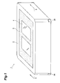
FIG 1 ] is a perspective view of an optical transmitting and receiving device according to a first embodiment. - [
FIG 2 ] is an end view taken along the line II-II shown inFIG 1 . - [
FIG 3 ] is an exploded perspective view of a main unit of the optical transmitting and receiving device shown inFIG 1 . - [
FIG 4 ] is an end view, corresponding toFIG 2 , of an optical transmitting and receiving device according to a second embodiment. - 1, 50 ... Optical transmitting and receiving device, 2 ... Enclosure, 3 ... Light blocking resin portion, 4 ... Main unit, 5 ... Base, 7 ... First cavity (first recess), 8 ... Second cavity (second recess), 9 ... LD (light emitting element), 12 ... PD (light receiving element), 20 ... Light blocking member, 22 ... Opening (first light transmitting hole), 23 ... Pinhole (second light transmitting hole), 27 ... Light transmitting member, 28 ... Groove, 30 ... Cavity (recess).
- Preferred embodiments of the present invention shall now be described in detail with reference to the drawings. In the drawings, portions that are the same or equivalent shall be provided with the same symbol and redundant description shall be omitted.
- As shown in
FIGS. 1 and2 , an optical transmitting and receivingdevice 1 according to a first embodiment includes anenclosure 2, formed of a plastic material to a form of a rectangular parallelepiped cup that opens to a front. Inside theenclosure 2 is disposed amain unit 4, incorporating an LD (light emitting element) 9, emitting light toward the front, and a PD (light receiving element) 12, receiving light illuminated from the front, and a peripheral region of themain unit 4 inside theenclosure 2 is filled with a lightblocking resin portion 3, having a light blocking property. The lightblocking resin portion 3 is constituted of a light blocking resin, such as a silicone resin containing an insulation-coated carbon filler, fixes themain unit 4 inside theenclosure 2, and reduces influence of disturbance light made incident onto thePD 12 from the periphery of themain unit 4. - As shown in
FIGS. 2 and3 , themain unit 4 has abase 5 at a bottom surface side of an interior of theenclosure 2. Thebase 5 is formed of silicon, which is a semiconductor material, to a form of a rectangular plate with a width of 2.8mm, a length of 6.0mm, and a thickness of 1.0mm, and a first cavity (first recess) 7 and a second cavity (first recess) 8 of recessed forms are formed in afront surface 5a of thebase 5. TheLD 9 is disposed inside thefirst cavity 7 and is electrically connected to anLD anode 10 and anLD cathode 11 to be described below. ThePD 12 is disposed inside thesecond cavity 8 and is electrically connected to aPD anode 13 and aPD cathode 14 to be described below. - The
cavities base 5. Specifically, thecavities cavities base 5 and making an etchant act on openings of the mask. After etching, the SiN mask is removed and thereafter, aninsulating film 40, formed for example of SiO2 and having a thickness of 1.5µm, is formed by thermal oxidation on at least surfaces of the cavities and a surface of the substrate. - The LD 9 uses, for example, a VCSEL (surface emitting laser), constituted of a compound semiconductor material and having a thickness of 0.2mm, and emits light of a wavelength of 850nm. With the
LD 9, anLD terminal electrode 15 is disposed on a front end surface and anLD terminal electrode 16 is disposed on a rear end surface. ThePD 12 uses, for example, an Si-PD or a GaAs-PD, constituted of a semiconductor material and having a thickness of 0.3mm. With thePD 12, aPD terminal electrode 17 and aPD terminal electrode 18 is disposed on a front end surface. - The material of the
PD 12 is selected according to the wavelength of the light emitted by theLD 9. For example, when the wavelength of the light emitted by theLD 9 is 780nm, Si or GaAs is used as the material ofPD 12, and when the wavelength of the light emitted by theLD 9 is 1.31µm, InGaAs is used as the material ofPD 12. - On the insulating
film 40 on thefront surface 5a of thesubstrate 5 and inner surfaces of thecavities base wiring portion 19 is formed in a predetermined pattern, for example, from a laminated film of Al, Ti-Pt-Au or a laminated film of Cr-Pt-Au. Thebase wiring portion 19 has theLD anode 10 and theLD cathode 11 at thefirst cavity 7 side, and has thePD anode 13 and thePD cathode 14 at thesecond cavity 8 side. As shown inFIGS. 1 and2 , theLD anode 10, theLD cathode 11, thePD anode 13, and thePD cathode 14 are electrically connected viawires 24 to lead-outelectrodes 26, formed at four corners of a bottom portion of theenclosure 2 so as to lead out the electrodes from a front surface to a rear surface of the bottom portion. TheLD terminal electrode 16 of theLD 9 is electrically connected, for example, via solder or conductive resin, etc., to thebase wiring portion 19 formed on the insulatingfilm 40 on a bottom surface of thefirst cavity 7, and theLD terminal electrode 15 of theLD 9 is electrically connected, for example, via a wire (not shown), to thebase wiring portion 19 formed on the insulatingfilm 40 on thefront surface 5a of thebase 5. TheLD 9 is thereby electrically connected to theLD anode 10 and theLD cathode 11, respectively. - Returning now to
FIGS. 2 and3 , alight blocking member 20, formed, for example, by forming a silicon substrate, coated with insulatingfilms 41 constituted of SiO2 to a rectangular plate form with a thickness of 0.15mm to 0.30mm, is laminated and fixed by abump bond 21 on the insulatingfilm 40 on thefront surface 5a of thebase 5. As examples of a material of thebump bond 21, Au-, Ni-, Cu-, AuSn-, and SnAg-based solders can be cited. Here, thebump bond 21 is preferably lined along a portion between thefirst cavity 7 and thesecond cavity 8 to prevent light, emitted from theLD 9, from reaching thePD 12 via a gap between thesubstrate 5 and thelight blocking member 20. A light blocking portion may be formed at this portion by coating or filling with a light blocking material. - In the
light blocking member 20 are formed an opening (first light transmitting hole) 22, disposed at a position corresponding to thefirst cavity 7, and a pinhole (second light transmitting hole) 23, disposed at a position corresponding to thesecond cavity 8. Theopening 22 guides the light, emitted from theLD 9, to an exterior. Thepinhole 23 guides scattered light from the exterior to thePD 12 and prevents entry of disturbance light and unwanted light from the exterior from becoming incident on thePD 12. Theopening 22 and thepinhole 23 are formed, for example, by applying dry etching to the silicon substrate that is to be thelight blocking member 20, and thepinhole 23 is configured to have a high aspect ratio. - The
pinhole 23 is formed at a position corresponding to a light receiving surface of thePD 12 and a diameter thereof is set, for example, to 30µm to 90µm. This is because when the diameter of thepinhole 23 is greater than 90µm, noise, due to disturbance light and unwanted light from the exterior that are detected by thePD 12, increases, and because when the diameter of thepinhole 23 is less than 30µm, the light received by thePD 12 lessens and an output from thePD 12 lessens. - On the insulating
film 41 on arear surface 20b of thelight blocking member 20, a light blockingmember wiring portion 25 is formed in a predetermined pattern and is electrically connected via thebump bond 21 to thebase wiring portion 19. ThePD terminal electrodes PD 12 are electrically connected by the bump bonds 21 (by so-called flip-chip bonding) to portions of the light blockingmember wiring portion 25 corresponding to thesecond cavity 8. ThePD 12 is thereby electrically connected to thePD anode 13 and thePD cathode 14, respectively. - A
light transmitting member 27, formed, for example, by forming an alkali-containing borosilicate glass to a rectangular plate form with a thickness of 0.3mm for transmission of the light emitted from theLD 9 and the scattered light from the exterior, is laminated and fixed by a resin on the insulatingfilm 41 on afront surface 20a of thelight blocking member 20. Thelight transmitting member 27 increases a mechanical strength of thelight blocking member 20 and seals and thereby packages thefirst cavity 7 and thesecond cavity 8 of thebase 5. Because thelight transmitting member 27 is fixed to thelight blocking member 20, a thermal expansion coefficient of thelight transmitting member 27 and a thermal expansion coefficient of thelight blocking member 20 are made substantially equal. Thelight blocking member 20 and thelight transmitting member 27 may be fixed by anodic bonding, and in this case, the insulatingfilm 41 is made unnecessary. - Here, whereas with the conventional optical transmitting and receiving device, it was difficult to fix the light transmitting member and there were thus cases where disturbance light became incident on the light receiving element due to inadequate fixing of the light transmitting member, with the present embodiment, the
light transmitting member 27 is laminated and fixed on thefront surface 20a of thelight blocking member 20 and the peripheral region of themain unit 4 inside theenclosure 2 is filled with the light blockingresin portion 3 to reliably fix thelight transmitting member 27 as described above. - With the light transmitting and receiving
device 1, agroove 28, passing between theopening 22 and thepinhole 23 as viewed from the front (upper side in the figure) and having both ends open toside surfaces 27c of thelight transmitting member 27, is formed in afront surface 27a of thelight transmitting member 27, and the light blockingresin portion 3 reaches an interior of thegroove 28. Thegroove 28 is formed, for example, by a dicing process, a width thereof is 100µm to 200µm, and a bottom surface (deepest portion) 28a thereof is thefront surface 20a of thelight blocking member 20. - The
bottom surface 28a of thegroove 28 is positioned more to the rear (toward the lower side in the figure) than a front end surface (front end) 2a of theenclosure 2. Thus, when the light blocking resin is made to flow in up to thefront end surface 2a of theenclosure 2 to form the light blockingresin portion 3, the light blocking resin can be made to flow in reliably and easily into thegroove 28 from both ends thereof by a capillary phenomenon and the light blockingresin portion 3 can thereby be made to reach the interior of thegroove 28. - Here, the light blocking resin is made to flow in up to the
front end surface 2a of theenclosure 2, and in order to prevent attachment of the light blocking resin on thefront surface 27a of thelight transmitting member 27, thefront surface 27a of thelight transmitting member 27 is positioned more to the front than thefront end surface 2a of theenclosure 2. - In using the optical transmitting and receiving
device 1 configured as described above, first, a voltage is applied to theLD anode 10 and theLD cathode 11 of thebase wiring portion 19 to make light be emitted from theLD 9, disposed inside thefirst cavity 7 of thebase 5. The light passes through theopening 22, formed in thelight blocking member 20, and is emitted to the exterior upon being transmitted through thelight transmitting member 27. The light emitted to the exterior is scattered, etc., by an object, and a portion of scattered light thus scattered propagates in a direction opposite a direction of propagation of the light emitted from theLD 9 and is transmitted through thelight transmitting member 27, passes through thepinhole 23 formed in thelight blocking member 20, and reaches thePD 12, disposed in thesecond cavity 8 of thebase 5. An electric signal that is in accordance to the arrived light is thus obtained from thePD anode 13 and thePD cathode 14 of thebase wiring portion 19. - As described above, with the optical transmitting and receiving
device 1 according to the first embodiment, thegroove 28, passing between theopening 22 and thepinhole 23 as viewed from the front and having both ends open to the side surfaces 27c of thelight transmitting member 27, is formed on thefront surface 27a of thelight transmitting member 27, and the light blockingresin portion 3 reaches the interior of thegroove 28. Thus, even if a portion of the light emitted from theLD 9 undergoes multiple reflection inside thelight transmitting member 27, the multiply reflected light is prevented by the light blockingresin portion 3 in thegroove 28 from reaching thePD 12 as unwanted light. Detection of noise current due to the unwanted light can thereby be prevented and incident light from the exterior can be detected with high precision. - Furthermore, by the
bottom surface 28a of thegroove 28 being positioned at thefront surface 20a of thelight blocking member 20, blocking of light between theLD 9 and thePD 12 can be secured reliably. - Also, by forming the lead-out
electrodes 26 at the four corners of the bottom portion of theenclosure 2 so as to lead out the electrodes from the front surface to the rear surface of the bottom portion, application of voltage to the light emitting element and take-out of an electrical signal from the light receiving element, which were problematic with the conventional optical transmitting and receiving device, can be performed favorably. - An optical transmitting and receiving
device 50 according to a second embodiment differs from the optical transmitting and receivingdevice 1 according to the first embodiment in the shape of thebase 5. That is, with the optical transmitting and receivingdevice 50 according to the second embodiment, a cavity (recess) 30, in which theLD 9 and thePD 12 are disposed, is formed in thefront surface 5a of thebase 5 as shown inFIG 4 . Alight blocking portion 31, formed of a light blocking resin, is disposed between the light blockingmember 20 and thePD 12 so as to surround alight receiving surface 12a of thePD 12. Incidence of disturbance light and unwanted light due to emitted light from theLD 9, etc., onto thePD 12 is thereby prevented. - The same actions and effects as those of the optical transmitting and receiving
device 1 according to the first embodiment are also exhibited by the optical transmitting and receivingdevice 50 according to the second embodiment configured as described above. - Although preferred embodiments of the present invention were described above, the present invention is not limited to the above embodiments.
- For example, although with the above-described embodiments, both ends of the
groove 28 open to the side surfaces 27 of thelight transmitting member 27, as long as one end of thegroove 28 is opened to theside surface 27c, the light blocking resin can be made to flow reliably and easily into thegroove 28 in making the light blocking resin flow inside theenclosure 2 to form the light blockingresin portion 3, and the light blockingresin portion 3 can thereby be made to reach the interior of thegroove 28. - Also, although with the above-described embodiments, the
bottom surface 28a of thegroove 28 is made thefront surface 20a of thelight blocking member 20, thebottom surface 28a may be positioned more to the rear than thefront surface 20a instead. - With the present invention, incident light from an exterior can be detected with high precision.
Claims (8)
- An optical transmitting and receiving device comprising: a main unit, in turn comprising:a light emitting element, for emitting light toward a front;a light receiving element, for receiving light illuminated from the front;a base, having a first recess, in which the light emitting element is positioned, and a second recess, in which the light receiving element is positioned, formed on a front surface;a light blocking member, disposed on the front surface side of the base and having formed therein a first light passage hole, through which the light emitted from the light emitting element passes, and a second light passage hole, through which the light to be received by the light receiving element passes; anda light transmitting member, disposed on a front surface side of the light blocking member and through which is transmitted the light emitted from the light emitting element and the light to be received by the light receiving element;an enclosure, formed so as to open toward the front and with which the main unit is positioned at an inner side thereof; anda light blocking resin portion, filling a region surrounding the main unit inside the enclosure;wherein a groove, passing between the first light passage hole and the second light passage hole as viewed from the front and having at least one end opened to a side surface of the light transmitting member, is formed in a front surface of the light transmitting member, andthe light blocking resin portion reaches an interior of the groove.
- An optical transmitting and receiving device comprising: a main unit, in turn comprising:a light emitting element, for emitting light toward a front;a light receiving element, for receiving light illuminated from the front;a base, having a recess, in which the light emitting element and the light receiving element are positioned, formed on a front surface;a light blocking member, disposed on the front surface side of the base and having formed therein a first light passage hole, through which the light emitted from the light emitting element passes, and a second light passage hole, through which the light to be received by the light receiving element passes; anda light transmitting member, disposed on a front surface side of the light blocking member and through which is transmitted the light emitted from the light emitting element and the light to be received by the light receiving element;an enclosure, formed so as to open toward the front and with which the main unit is positioned at an inner side thereof; anda light blocking resin portion, filling a region surrounding the main unit inside the enclosure;wherein a groove, passing between the first light passage hole and the second light passage hole as viewed from the front and having at least one end opened to a side surface of the light transmitting member, is formed in a front surface of the light transmitting member, andthe light blocking resin portion reaches an interior of the groove.
- The optical transmitting and receiving device according to Claim 1, wherein a deepest portion of the groove is positioned at the front surface or more to the rear than the front surface of the light blocking member.
- The optical transmitting and receiving device according to Claim 2, wherein a deepest portion of the groove is positioned at the front surface or more to the rear than the front surface of the light blocking member.
- The optical transmitting and receiving device according to Claim 1, wherein the deepest portion of the groove is positioned more to the rear than a front end of the enclosure.
- The optical transmitting and receiving device according to Claim 2, wherein the deepest portion of the groove is positioned more to the rear than a front end of the enclosure.
- The optical transmitting and receiving device according to Claim 1, wherein the groove has both ends opened to side surfaces of the light transmitting member.
- The optical transmitting and receiving device according to Claim 2, wherein the groove has both ends opened to side surfaces of the light transmitting member.
Applications Claiming Priority (2)
| Application Number | Priority Date | Filing Date | Title |
|---|---|---|---|
| JP2006139146A JP4943739B2 (en) | 2006-05-18 | 2006-05-18 | Optical transceiver device |
| PCT/JP2007/059951 WO2007135897A1 (en) | 2006-05-18 | 2007-05-15 | Light transmitting/receiving device |
Publications (3)
| Publication Number | Publication Date |
|---|---|
| EP2023397A1 true EP2023397A1 (en) | 2009-02-11 |
| EP2023397A4 EP2023397A4 (en) | 2014-06-25 |
| EP2023397B1 EP2023397B1 (en) | 2015-03-25 |
Family
ID=38723210
Family Applications (1)
| Application Number | Title | Priority Date | Filing Date |
|---|---|---|---|
| EP07743386.0A Ceased EP2023397B1 (en) | 2006-05-18 | 2007-05-15 | Light transmitting/receiving device |
Country Status (7)
| Country | Link |
|---|---|
| US (1) | US7826695B2 (en) |
| EP (1) | EP2023397B1 (en) |
| JP (1) | JP4943739B2 (en) |
| KR (1) | KR20090019763A (en) |
| CN (1) | CN101529600B (en) |
| TW (1) | TWI392249B (en) |
| WO (1) | WO2007135897A1 (en) |
Cited By (1)
| Publication number | Priority date | Publication date | Assignee | Title |
|---|---|---|---|---|
| WO2018153464A1 (en) * | 2017-02-23 | 2018-08-30 | Osram Opto Semiconductors Gmbh | Sensor element |
Families Citing this family (5)
| Publication number | Priority date | Publication date | Assignee | Title |
|---|---|---|---|---|
| KR100992778B1 (en) | 2008-05-23 | 2010-11-05 | 엘지이노텍 주식회사 | Light emitting device package and method for manufacturing the same |
| JP5908627B2 (en) * | 2015-03-13 | 2016-04-26 | エスアイアイ・セミコンダクタ株式会社 | Optical sensor device |
| JP6462904B2 (en) * | 2016-01-25 | 2019-01-30 | 京セラ株式会社 | Measurement sensor package and measurement sensor |
| WO2019160001A1 (en) * | 2018-02-14 | 2019-08-22 | 古河電気工業株式会社 | Optical module |
| CN112425015A (en) | 2018-05-11 | 2021-02-26 | Lg伊诺特有限公司 | Surface emitting laser package and light emitting device including the same |
Family Cites Families (16)
| Publication number | Priority date | Publication date | Assignee | Title |
|---|---|---|---|---|
| JPH0226080A (en) * | 1988-07-14 | 1990-01-29 | Olympus Optical Co Ltd | Semiconductor device |
| JPH05240701A (en) * | 1992-02-28 | 1993-09-17 | Hamamatsu Photonics Kk | Semiconductor photodetector |
| JP2000075155A (en) * | 1998-09-02 | 2000-03-14 | Nippon Telegr & Teleph Corp <Ntt> | Optical module |
| JP3990846B2 (en) * | 1999-08-27 | 2007-10-17 | キヤノン株式会社 | Planar optical element, method for manufacturing the same, and apparatus using the same |
| JP3997666B2 (en) * | 1999-08-31 | 2007-10-24 | 株式会社デンソー | Pulse wave sensor |
| JP3722279B2 (en) * | 2001-01-26 | 2005-11-30 | 日本電気株式会社 | Optical transceiver module |
| JP2003004855A (en) * | 2001-06-26 | 2003-01-08 | Hamamatsu Photonics Kk | Radiation detector |
| JP2003329895A (en) * | 2002-05-14 | 2003-11-19 | Sony Corp | Optical link device |
| JP3838164B2 (en) * | 2002-06-18 | 2006-10-25 | 住友電気工業株式会社 | Optical communication element and method for manufacturing optical communication element |
| KR100460840B1 (en) * | 2002-08-09 | 2004-12-09 | 한국전자통신연구원 | Optical modules for suppressing the optical and electrical crosstalk simultaneously |
| JP3882756B2 (en) * | 2003-01-30 | 2007-02-21 | 日本電信電話株式会社 | Blood flow sensor and blood flow meter |
| US7248800B2 (en) * | 2003-05-30 | 2007-07-24 | Canon Kabushiki Kaisha | Optical receiver, optical transmitter and optical transceiver |
| JP2005116670A (en) * | 2003-09-18 | 2005-04-28 | New Japan Radio Co Ltd | Manufacturing method for light receiving/emitting device |
| JP2005234464A (en) * | 2004-02-23 | 2005-09-02 | Tdk Corp | Optical transceiver and optical module used therefor |
| EP1645898A1 (en) * | 2004-10-05 | 2006-04-12 | STMicroelectronics S.r.l. | Optical communication module |
| JP4708214B2 (en) * | 2006-02-23 | 2011-06-22 | 浜松ホトニクス株式会社 | Optical transceiver device |
-
2006
- 2006-05-18 JP JP2006139146A patent/JP4943739B2/en not_active Expired - Fee Related
-
2007
- 2007-05-15 EP EP07743386.0A patent/EP2023397B1/en not_active Ceased
- 2007-05-15 CN CN2007800140128A patent/CN101529600B/en not_active Expired - Fee Related
- 2007-05-15 WO PCT/JP2007/059951 patent/WO2007135897A1/en not_active Ceased
- 2007-05-15 US US12/301,142 patent/US7826695B2/en active Active
- 2007-05-15 KR KR1020087020372A patent/KR20090019763A/en not_active Withdrawn
- 2007-05-17 TW TW096117594A patent/TWI392249B/en not_active IP Right Cessation
Cited By (2)
| Publication number | Priority date | Publication date | Assignee | Title |
|---|---|---|---|---|
| WO2018153464A1 (en) * | 2017-02-23 | 2018-08-30 | Osram Opto Semiconductors Gmbh | Sensor element |
| US10868209B2 (en) | 2017-02-23 | 2020-12-15 | Osram Oled Gmbh | Sensor element |
Also Published As
| Publication number | Publication date |
|---|---|
| KR20090019763A (en) | 2009-02-25 |
| EP2023397A4 (en) | 2014-06-25 |
| EP2023397B1 (en) | 2015-03-25 |
| WO2007135897A1 (en) | 2007-11-29 |
| US7826695B2 (en) | 2010-11-02 |
| JP2007311552A (en) | 2007-11-29 |
| US20090232451A1 (en) | 2009-09-17 |
| TWI392249B (en) | 2013-04-01 |
| CN101529600A (en) | 2009-09-09 |
| CN101529600B (en) | 2010-12-15 |
| JP4943739B2 (en) | 2012-05-30 |
| TW200807912A (en) | 2008-02-01 |
Similar Documents
| Publication | Publication Date | Title |
|---|---|---|
| CN101371373B (en) | Optical transmission/reception device | |
| EP2023397B1 (en) | Light transmitting/receiving device | |
| CN110867722B (en) | TO package with feedthrough made of glass | |
| US8777496B2 (en) | Optical device | |
| CN101569023A (en) | Housing for an optoelectronic component and arrangement of the optoelectronic component in the housing | |
| EP3358320A1 (en) | Light detection device | |
| JP3684305B2 (en) | Semiconductor laser coupling device and semiconductor light receiving device | |
| US20070228405A1 (en) | Electronic component and electronic component module | |
| US20200343686A1 (en) | Light-emitting device | |
| US20110215366A1 (en) | Light emitting device | |
| US11316076B2 (en) | Light emitting diode package and light emitting module including the same | |
| CN100487929C (en) | Light-emitting device and method of making same | |
| JP3483102B2 (en) | Optical element mounting body | |
| KR20210116623A (en) | Packages and electronic devices for mounting electronic devices | |
| CN107658691B (en) | Optical semiconductor device | |
| US20250158352A1 (en) | Laser module | |
| CN114008875B (en) | Semiconductor laser device and photoelectric ray deflection element of semiconductor laser device | |
| US7420216B2 (en) | Reflection type light-emitting diode device | |
| CN100502019C (en) | Optical device | |
| US20230061980A1 (en) | Opto-electric hybrid board | |
| WO2021039907A1 (en) | Optical element mounting package, electronic device, and electronic module | |
| JP5310375B2 (en) | Optical transmission module | |
| EP4535581A1 (en) | Laser device and package for mounting optical component | |
| JP2000323791A (en) | Assembly of vertical cavity surface emitting laser and photodetection monitor and method of assembling the same | |
| KR20180072766A (en) | Package for measuring sensor and measuring sensor |
Legal Events
| Date | Code | Title | Description |
|---|---|---|---|
| PUAI | Public reference made under article 153(3) epc to a published international application that has entered the european phase |
Free format text: ORIGINAL CODE: 0009012 |
|
| 17P | Request for examination filed |
Effective date: 20081127 |
|
| AK | Designated contracting states |
Kind code of ref document: A1 Designated state(s): AT BE BG CH CY CZ DE DK EE ES FI FR GB GR HU IE IS IT LI LT LU LV MC MT NL PL PT RO SE SI SK TR |
|
| AX | Request for extension of the european patent |
Extension state: AL BA HR MK RS |
|
| RBV | Designated contracting states (corrected) |
Designated state(s): DE FR GB |
|
| DAX | Request for extension of the european patent (deleted) | ||
| A4 | Supplementary search report drawn up and despatched |
Effective date: 20140522 |
|
| RIC1 | Information provided on ipc code assigned before grant |
Ipc: H01L 31/02 20060101AFI20140516BHEP Ipc: G02B 6/42 20060101ALI20140516BHEP Ipc: H01S 5/022 20060101ALI20140516BHEP |
|
| GRAP | Despatch of communication of intention to grant a patent |
Free format text: ORIGINAL CODE: EPIDOSNIGR1 |
|
| INTG | Intention to grant announced |
Effective date: 20141028 |
|
| GRAS | Grant fee paid |
Free format text: ORIGINAL CODE: EPIDOSNIGR3 |
|
| GRAA | (expected) grant |
Free format text: ORIGINAL CODE: 0009210 |
|
| AK | Designated contracting states |
Kind code of ref document: B1 Designated state(s): DE FR GB |
|
| REG | Reference to a national code |
Ref country code: GB Ref legal event code: FG4D |
|
| REG | Reference to a national code |
Ref country code: DE Ref legal event code: R096 Ref document number: 602007040781 Country of ref document: DE Effective date: 20150507 |
|
| REG | Reference to a national code |
Ref country code: DE Ref legal event code: R097 Ref document number: 602007040781 Country of ref document: DE |
|
| PLBE | No opposition filed within time limit |
Free format text: ORIGINAL CODE: 0009261 |
|
| STAA | Information on the status of an ep patent application or granted ep patent |
Free format text: STATUS: NO OPPOSITION FILED WITHIN TIME LIMIT |
|
| 26N | No opposition filed |
Effective date: 20160105 |
|
| REG | Reference to a national code |
Ref country code: FR Ref legal event code: PLFP Year of fee payment: 10 |
|
| REG | Reference to a national code |
Ref country code: FR Ref legal event code: PLFP Year of fee payment: 11 |
|
| REG | Reference to a national code |
Ref country code: FR Ref legal event code: PLFP Year of fee payment: 12 |
|
| PGFP | Annual fee paid to national office [announced via postgrant information from national office to epo] |
Ref country code: DE Payment date: 20190430 Year of fee payment: 13 |
|
| PGFP | Annual fee paid to national office [announced via postgrant information from national office to epo] |
Ref country code: FR Payment date: 20190410 Year of fee payment: 13 |
|
| PGFP | Annual fee paid to national office [announced via postgrant information from national office to epo] |
Ref country code: GB Payment date: 20190515 Year of fee payment: 13 |
|
| REG | Reference to a national code |
Ref country code: DE Ref legal event code: R119 Ref document number: 602007040781 Country of ref document: DE |
|
| GBPC | Gb: european patent ceased through non-payment of renewal fee |
Effective date: 20200515 |
|
| PG25 | Lapsed in a contracting state [announced via postgrant information from national office to epo] |
Ref country code: FR Free format text: LAPSE BECAUSE OF NON-PAYMENT OF DUE FEES Effective date: 20200531 Ref country code: GB Free format text: LAPSE BECAUSE OF NON-PAYMENT OF DUE FEES Effective date: 20200515 |
|
| PG25 | Lapsed in a contracting state [announced via postgrant information from national office to epo] |
Ref country code: DE Free format text: LAPSE BECAUSE OF NON-PAYMENT OF DUE FEES Effective date: 20201201 |