EP2023109A2 - Load sensor with semiconductive strain gauges - Google Patents
Load sensor with semiconductive strain gauges Download PDFInfo
- Publication number
- EP2023109A2 EP2023109A2 EP08013877A EP08013877A EP2023109A2 EP 2023109 A2 EP2023109 A2 EP 2023109A2 EP 08013877 A EP08013877 A EP 08013877A EP 08013877 A EP08013877 A EP 08013877A EP 2023109 A2 EP2023109 A2 EP 2023109A2
- Authority
- EP
- European Patent Office
- Prior art keywords
- pin
- load sensor
- detection rod
- strain
- sensor
- Prior art date
- Legal status (The legal status is an assumption and is not a legal conclusion. Google has not performed a legal analysis and makes no representation as to the accuracy of the status listed.)
- Granted
Links
- 238000001514 detection method Methods 0.000 claims abstract description 122
- 239000004065 semiconductor Substances 0.000 claims abstract description 74
- 239000000463 material Substances 0.000 claims abstract description 48
- 230000035939 shock Effects 0.000 claims abstract description 38
- 238000009792 diffusion process Methods 0.000 claims description 53
- XUIMIQQOPSSXEZ-UHFFFAOYSA-N Silicon Chemical compound [Si] XUIMIQQOPSSXEZ-UHFFFAOYSA-N 0.000 claims description 31
- 229910052710 silicon Inorganic materials 0.000 claims description 31
- 239000010703 silicon Substances 0.000 claims description 31
- 239000013078 crystal Substances 0.000 claims description 23
- 239000000758 substrate Substances 0.000 claims description 23
- 230000007935 neutral effect Effects 0.000 claims description 10
- 238000004519 manufacturing process Methods 0.000 claims description 6
- 239000002184 metal Substances 0.000 claims description 6
- 238000000034 method Methods 0.000 claims description 5
- 239000003822 epoxy resin Substances 0.000 claims description 4
- 229920000647 polyepoxide Polymers 0.000 claims description 4
- 239000011347 resin Substances 0.000 claims description 2
- 229920005989 resin Polymers 0.000 claims description 2
- 230000035945 sensitivity Effects 0.000 description 15
- 230000000694 effects Effects 0.000 description 9
- 238000005452 bending Methods 0.000 description 5
- 238000005259 measurement Methods 0.000 description 5
- XLYOFNOQVPJJNP-UHFFFAOYSA-N water Substances O XLYOFNOQVPJJNP-UHFFFAOYSA-N 0.000 description 3
- 230000006835 compression Effects 0.000 description 2
- 238000007906 compression Methods 0.000 description 2
- 230000008878 coupling Effects 0.000 description 2
- 238000010168 coupling process Methods 0.000 description 2
- 238000005859 coupling reaction Methods 0.000 description 2
- 238000010586 diagram Methods 0.000 description 2
- 239000012535 impurity Substances 0.000 description 2
- 229910021421 monocrystalline silicon Inorganic materials 0.000 description 2
- 230000002093 peripheral effect Effects 0.000 description 2
- 239000011343 solid material Substances 0.000 description 2
- 239000011800 void material Substances 0.000 description 2
- VYPSYNLAJGMNEJ-UHFFFAOYSA-N Silicium dioxide Chemical compound O=[Si]=O VYPSYNLAJGMNEJ-UHFFFAOYSA-N 0.000 description 1
- 239000002274 desiccant Substances 0.000 description 1
- 230000006866 deterioration Effects 0.000 description 1
- 239000011261 inert gas Substances 0.000 description 1
- 239000004850 liquid epoxy resins (LERs) Substances 0.000 description 1
- 238000012986 modification Methods 0.000 description 1
- 230000004048 modification Effects 0.000 description 1
- 229920001296 polysiloxane Polymers 0.000 description 1
- 238000004904 shortening Methods 0.000 description 1
- 239000000741 silica gel Substances 0.000 description 1
- 229910002027 silica gel Inorganic materials 0.000 description 1
- 229920002379 silicone rubber Polymers 0.000 description 1
- 230000001629 suppression Effects 0.000 description 1
- 238000004078 waterproofing Methods 0.000 description 1
Images





Classifications
-
- G—PHYSICS
- G01—MEASURING; TESTING
- G01L—MEASURING FORCE, STRESS, TORQUE, WORK, MECHANICAL POWER, MECHANICAL EFFICIENCY, OR FLUID PRESSURE
- G01L1/00—Measuring force or stress, in general
- G01L1/20—Measuring force or stress, in general by measuring variations in ohmic resistance of solid materials or of electrically-conductive fluids; by making use of electrokinetic cells, i.e. liquid-containing cells wherein an electrical potential is produced or varied upon the application of stress
- G01L1/22—Measuring force or stress, in general by measuring variations in ohmic resistance of solid materials or of electrically-conductive fluids; by making use of electrokinetic cells, i.e. liquid-containing cells wherein an electrical potential is produced or varied upon the application of stress using resistance strain gauges
- G01L1/2206—Special supports with preselected places to mount the resistance strain gauges; Mounting of supports
- G01L1/2218—Special supports with preselected places to mount the resistance strain gauges; Mounting of supports the supports being of the column type, e.g. cylindric, adapted for measuring a force along a single direction
- G01L1/2225—Special supports with preselected places to mount the resistance strain gauges; Mounting of supports the supports being of the column type, e.g. cylindric, adapted for measuring a force along a single direction the direction being perpendicular to the central axis
-
- G—PHYSICS
- G01—MEASURING; TESTING
- G01L—MEASURING FORCE, STRESS, TORQUE, WORK, MECHANICAL POWER, MECHANICAL EFFICIENCY, OR FLUID PRESSURE
- G01L1/00—Measuring force or stress, in general
- G01L1/18—Measuring force or stress, in general using properties of piezo-resistive materials, i.e. materials of which the ohmic resistance varies according to changes in magnitude or direction of force applied to the material
-
- G—PHYSICS
- G01—MEASURING; TESTING
- G01L—MEASURING FORCE, STRESS, TORQUE, WORK, MECHANICAL POWER, MECHANICAL EFFICIENCY, OR FLUID PRESSURE
- G01L1/00—Measuring force or stress, in general
- G01L1/26—Auxiliary measures taken, or devices used, in connection with the measurement of force, e.g. for preventing influence of transverse components of force, for preventing overload
-
- G—PHYSICS
- G01—MEASURING; TESTING
- G01L—MEASURING FORCE, STRESS, TORQUE, WORK, MECHANICAL POWER, MECHANICAL EFFICIENCY, OR FLUID PRESSURE
- G01L5/00—Apparatus for, or methods of, measuring force, work, mechanical power, or torque, specially adapted for specific purposes
- G01L5/16—Apparatus for, or methods of, measuring force, work, mechanical power, or torque, specially adapted for specific purposes for measuring several components of force
- G01L5/161—Apparatus for, or methods of, measuring force, work, mechanical power, or torque, specially adapted for specific purposes for measuring several components of force using variations in ohmic resistance
- G01L5/162—Apparatus for, or methods of, measuring force, work, mechanical power, or torque, specially adapted for specific purposes for measuring several components of force using variations in ohmic resistance of piezoresistors
-
- Y—GENERAL TAGGING OF NEW TECHNOLOGICAL DEVELOPMENTS; GENERAL TAGGING OF CROSS-SECTIONAL TECHNOLOGIES SPANNING OVER SEVERAL SECTIONS OF THE IPC; TECHNICAL SUBJECTS COVERED BY FORMER USPC CROSS-REFERENCE ART COLLECTIONS [XRACs] AND DIGESTS
- Y10—TECHNICAL SUBJECTS COVERED BY FORMER USPC
- Y10T—TECHNICAL SUBJECTS COVERED BY FORMER US CLASSIFICATION
- Y10T29/00—Metal working
- Y10T29/49—Method of mechanical manufacture
- Y10T29/49002—Electrical device making
- Y10T29/49082—Resistor making
- Y10T29/49103—Strain gauge making
Definitions
- the present invention relates to a load sensor which can detect a load at a high precision.
- a pin type load sensor using a pin for coupling the parts used in a coupling portion of the machine as a load sensor As shown in JP-A-10-38713 .
- the pin type load sensor is structured such as to measure a strain of the pin generated by a load application by a strain measuring apparatus so as to detect the load.
- a metal resistance type strain gauge is used as the strain measuring apparatus.
- the inventors of the present invention have invented a pin type load sensor making use of a semiconductor strain sensor shown in JP-A-2005-114443 , for achieving a pin type load sensor which has a small zero point fluctuation of an output, has a high noise resistance, and can be driven by a battery for a long time at a low electric power consumption.
- the semiconductor strain sensor uses an impurity diffusion resistance (hereinafter, refer to as a diffusion resistance) obtained by introducing an impurity to a single crystal silicon substrate as a strain sensitive resistance, and has a feature that a strain sensitivity is high and a zero point fluctuation is very small.
- an output of the semiconductor strain sensor is such a great voltage that can detect the load without amplifying a signal by an amplifier or the like, and has a feature of being hard to be affected by the noise.
- the strain sensitivity is low in the strain gauge, it is necessary to detect by amplifying the strain of the pin generated by the load application. Accordingly, a large hole is provided in an inner portion of the pin, the strain gauge is provided in an inner wall, and the strain generated in the inner wall is directly measure. In other words, the structure is made such that the strain at the strain measuring position in the pin inner portion is enlarged.
- the detection block has a complicated structure in such a manner that the strain of the pin can be amplified by the detection block. Further, the inner wall of the pin and the detection block directly comes into contact with each other, whereby the load applied to the pin is directly transmitted to the detection block, and the strain at the strain measuring position is enlarged.
- the load sensor using the semiconductor strain sensor since a main part of the semiconductor strain sensor is constituted by a single crystal silicon substrate, there is a risk that the strain sensor is broken if an excessive strain is generated in a pin type load cell at a time of applying a shock or the like. Accordingly, in the case that the semiconductor strain sensor is used in the pin type load cell, it is an important object to structure such that the excessive strain is not generated at the strain measuring position of the semiconductor strain sensor.
- an object of the present invention is to provide a load sensor which is driven by a low electric power consumption, can measure at a high precision, and has a high reliability without being broken.
- the object mentioned above can be achieved by providing a detection rod for detecting a strain in an inner portion of a hole formed near a center of a pin via a shock relaxation material and providing a semiconductor strain sensor in the detection rod, in a load sensor detecting a load applied to the pin from a strain generated in an inner portion of the pin.
- a load sensor including a pin having a hole provided in a region including a neutral axis, a detection rod provided in an inner portion of the hole, a semiconductor strain sensor provided in the detection rod, and a shock relaxation material provided between the detection rod and the pin in the inner portion of the hole.
- the detection rod is provided in the region including the neutral axis of the pin.
- Young's modulus of the shock relaxation material is lower than Young's modulus of the pin and the detection rod.
- a material of the shock relaxation material is an epoxy resin, and it is preferable that a material of the detection rod is a metal.
- the material of the detection rod is the same as the material of the pin.
- a cross sectional shape of the detection rod is a square, and it is preferable that a cross sectional shape of the detection rod is a flat plate.
- a longitudinal direction of the detection rod is in parallel to a longitudinal direction of the pin.
- the semiconductor strain sensor is provided in such a manner as to detect a shear strain of the detection rod, and it is preferable that the semiconductor strain sensor is provided with a diffusion layer on a surface of a silicon substrate, and is constructed by a bridge circuit constituted by four diffusion layers on the same substrate surface.
- the diffusion layer formed on the surface of the silicon substrate is constituted by a P type diffusion layer, and the bridge circuit is constructed by two diffusion resistances in which a longitudinal direction of the P type diffusion layer is in parallel to a direction ⁇ 110> of a silicon single crystal, and two P type diffusion layers which are perpendicular thereto.
- the direction ⁇ 110> of the silicon single crystal of the strain sensor is arranged in parallel to a direction of 45 degree with respect to the longitudinal direction of the pin. Further, it is preferable that power supply lines of the two or more strain sensors are held in common in the inner portion of the pin, and the number of the wiring drawn out to an outer portion of the pin from the two or more strain sensors is obtained by a formula (number of sensors x 2) + 2.
- the detection rod is constituted by a rectangular column having a square cross sectional shape, and the strain sensors are provided in two orthogonal surfaces of the rectangular columns.
- the detection rod is constituted by a circular column, and the strain sensor is provided at least on one surface of the circular column.
- a manufacturing method of a load sensor including a step of attaching a semiconductor strain sensor to a detection rod, a step of inserting the detection rod attaching the semiconductor strain sensor thereto into a hole provided in a region including a center shaft of a pin, and a step of filling a resin in the hole of the pin so as to form a shock relaxation material.
- the load applied to the pin is applied to the detection rod via the shock relaxation material, it is possible to relax the strain generated in the detection rod more than the strain generated in the inner wall of the pin, and even in the case that the excessive strain is generated in the pin such as the case that the shock load is applied or the like, it is possible to achieve the pin type load sensor having a high reliability without breaking the semiconductor strain sensor.
- Figs. 1 and 2 respectively show a vertical cross sectional structure and a transverse cross sectional structure of a load sensor in accordance with the present embodiment.
- a hole 1a is provided near a center of a pin 1
- a detection rod 2 for detecting a strain is provided in an inner portion of the hole 1a via a shock relaxation material 5.
- the detection rod 2 is provided with semiconductor strain sensors 3 and 4 each constituted by a silicon substrate.
- the detection rod 2 is arranged near a neutral axis 100 of the pin 1, and a longitudinal direction of the detection rod 2 is in parallel to a longitudinal direction of the pin 1.
- a cross sectional shape of the detection rod 2 is a flat plate shape, however, the detection rod 2 may be formed as a rectangular columnar shape or a circular columnar shape.
- Young's modulus of a material of the shock relaxation material 5 forming the shock relaxation layer of the pin 1 is lower than Young's modulus of a material of the pin 1 and the detection rod 2.
- this structure can be achieved by setting the material of the shock relaxation material 5 to an epoxy resin, setting the material of the pin 1 and the detection rod 2 to a metal.
- the semiconductor strain sensors 3 and 4 are structured by forming a diffusion layer on a surface of a silicon substrate, and is structured such that a bridge circuit is formed by four diffusion layers formed on the same substrate surface.
- the semiconductor strain sensor 3 is provided at a desired position of the strain detection rod 2. Further, the semiconductor strain sensor 3 is constituted by a silicon single crystal substrate, and four diffusion layers 30a, 30b, 30c and 30d are formed on the same substrate surface, for example, as shown in Fig. 7 .
- the bridge circuit is formed by these four diffusion layers.
- four diffusion layers 30a, 30b, 30c and 30d are constituted by a P type diffusion layer, and the bridge circuit is constructed by two diffusion layers in which a longitudinal direction of the P type diffusion layer is in parallel to a direction ⁇ 110> of the silicon single crystal, and two P type diffusion layers which are perpendicular thereto. Further, the direction ⁇ 110> of the silicon single crystal of the semiconductor strain sensors 3 and 4 is arranged in parallel to a direction which is 45 degree with respect to the longitudinal direction of the pin.
- the load applied to the pin 1 is applied to the detection rod 2 via the shock relaxation material 5, it is possible to relax the strain generated in the detection rod than the strain generated in the inner wall of the pin 1. Even in the case that an excessive strain is generated in the pin 1 such as a case that the shock load is applied or the like, it is possible to achieve a pin type load sensor having a high reliability without breaking the semiconductor strain sensor.
- the semiconductor strain sensors 3 and 4 can accurately detect the stress applied to the pin in such a manner as to separate per directing directions, by measuring the strain of the detection rod 2.
- This makes use of the structure in which the detection rod 2 has the longitudinal direction in the same direction as the longitudinal direction (an axial direction) of the pin 1 and the detection rod 2 is deformed in the same manner as the pin 1.
- the stress applied to the strain sensor is small, and it is possible to prevent the strain sensor from being broken.
- the strain sensor is provided in the inner wall of the hole of the pin 1 such as the conventional structure
- the shock relaxation material there can be considered to provide the shock relaxation material between the inner wall of the pin 1 and the strain sensor, however, a thickness of the shock relaxation material is limited, and it is impossible to enlarge an effect of the shock relaxation.
- the semiconductor strain sensors 3 and 4 are provided in the layered shock relaxation material 5 without setting the detection rod, the stress applied to the semiconductor strain sensors 3 and 4 becomes complicated, the force is applied from two shafts in a cross sectional direction of the pin, and it is impossible to detect only the strain in a desired detecting direction.
- the material of the shock relaxation material 5 is set to the epoxy resin, it is possible to fill the liquid epoxy resin in a gap of the hole, and thereafter harden. Accordingly, there can be obtained an effect that a manufacturing method is easy and a cost can be lowered.
- the semiconductor strain sensor is structured such that the diffusion layers are formed on the surface of the silicon substrate, and the bridge circuit constituted by four diffusion layers is constructed on the same substrate surface, it is easy to suppress a temperature drift. Further, since the bridge circuit is constructed by one chip, it is sufficient to install only one strain sensor in the detection rod. Accordingly, since it is not necessary to align the resistances constructing the bridge circuit, there can be obtained an effect that it is easy to manufacture, and a cost can be reduced on the basis of a shortening of a manufacturing time.
- the diffusion layer formed on the surface of the silicone substrate is constituted by the P type diffusion layer, and the bridge circuit is constructed by two diffusion layers in which the longitudinal direction of the P type diffusion layer is in parallel to the direction ⁇ 110> of the silicon single crystal, and two P type diffusion layers which are perpendicular thereto, there is obtained an effect that a sensitivity of the semiconductor strain sensors 3 and 4 is improved.
- the semiconductor strain sensors can be actuated as a four-active bridge circuit, it is possible to detect the strain generated in the detection rod at a high sensitivity.
- a shear load is applied to the pin type load sensor from a vertical direction to the longitudinal direction of the pin 1. Specifically, loads 64 and 66 having the same direction are applied to support surfaces 61 and 63 of the pin 1, and a load 65 having an opposite direction to the loads 64 and 66 is applied to an application surface 62. Accordingly, a shear deformation is generated in regions 67 and 68 in an inner portion of the pin 1. In other words, in the case that the pin 1 is exposed to the shear load, the shear deformation is generated in the detection rod 2 provided in the inner portion of the pin 1.
- a compression strain and a tensile strain are respectively generated in two orthogonal shafts in directions which are at 45 degree with respect to the longitudinal direction of the pin. It is possible to detect these strains by the semiconductor strain sensors 3 and 4 so as to calculate the load.
- the direction ⁇ 110> of the silicon single crystal of the semiconductor strain sensors 3 and 4 is arranged in parallel to the direction which is at 45 degree with respect to the longitudinal direction of the pin, as shown in Fig. 7 , it is possible to detect the shear strain generated in the pin 1 at a higher sensitivity.
- a vertical strain component in the direction of 45 degree with respect to the longitudinal direction comes to a two-axis strain field in which the tensile strain is generated in one direction (a direction x), and the compression strain is generated in the vertical direction thereto (a direction y), and the vertical strain becomes maximum.
- the bridge circuit is constructed by two diffusion layers in which the longitudinal direction is in parallel to the direction ⁇ 110> of the silicon single crystal (Si ⁇ 110>), and two P type diffusion layers which are vertical thereto, there is a feature that a strain sensitivity in parallel and vertical directions to the direction ⁇ 110> is great in the both, and a code of the strain sensitivity is inverted. Accordingly, there is an advantage that it is possible to detect the shear strain at a higher sensitivity by arranging the P type diffusion layer which is parallel and vertical to the direction ⁇ 110> of the silicon single crystal, in parallel to the longitudinal direction and the directions x and y in which the vertical strain becomes maximum.
- Fig. 7 shows the case that each of the lines of the outer shape of the semiconductor silicon substrate is in parallel to the direction ⁇ 100> of the silicon single crystal (Si ⁇ 100>), however, the semiconductor strain sensor may be structured, as shown in Fig. 8 , such that each of the lines of the outer shape is in parallel to the direction ⁇ 110> of the silicon single crystal (Si ⁇ 110>).
- the semiconductor strain sensors 3 and 4 in which the bridge circuit is constructed by two diffusion layers which are in parallel to the direction ⁇ 110> of the silicon single crystal, and two P type diffusion layers which are perpendicular thereto, however, the same effect can be obtained by forming the semiconductor strain sensors 3 and 4 in which the bridge circuit is constructed by two diffusion layers which are in parallel to the direction ⁇ 100> of the silicon single crystal, and two N type diffusion layers which are perpendicular thereto, and arranging the direction ⁇ 100> of the silicon single crystal of the semiconductor strain sensors 3 and 4 in parallel to the direction which is at 45 degree with respect to the longitudinal direction of the pin 1, as shown in Fig. 9 .
- the direction ⁇ 100> of the silicon single crystal of the semiconductor strain sensor in parallel to the direction which is at 45 degree with respect to the longitudinal direction of the pin. Accordingly, it is possible to detect the shear deformation of the detection rod 2 caused by the load applied to the pin, at a high sensitivity.
- the bridge circuit is manufactured by the P type diffusion layer which is vertical and parallel to the direction ⁇ 110> of the silicon single crystal, whereby there is an advantage that the sensitivity with respect to the strain in the surface outside direction becomes approximately zero, it is easy to detect only the strain of the detection rod, and the measurement error becomes small.
- two bridge circuits may be provided in the semiconductor strain sensor 3 provided in the detection rod 2.
- a bridge circuit formed by two diffusion layers 30a and 30c in which a longitudinal direction is in parallel to the direction ⁇ 110> of the silicon single crystal (Si ⁇ 110>), and two P type diffusion layers 30b and 30d which are perpendicular thereto and a bridge circuit formed by two diffusion layers in which a longitudinal direction is in parallel to the direction ⁇ 100> of the silicon single crystal, and two N type diffusion layers which are perpendicular thereto, on the same substrate.
- the bridge circuit is manufactured by the P type diffusion layer which is vertical and parallel to the direction ⁇ 110> of the silicon single crystal, so that there is an advantage that it becomes easy to detect only the strain of the detection rod, and the measurement error becomes small.
- two bridge circuits may be provided in the semiconductor sensor 3 provided in the detection rod 2.
- the bridge circuit formed by two diffusion layers 30a and 30c in which the longitudinal direction is in parallel to the direction ⁇ 110> of the silicon single crystal (Si ⁇ 110>), and two P type diffusion layers 30b and 30d which are perpendicular thereto are provided, and the bridge circuit formed by two diffusion layers in which the longitudinal direction is in parallel to the direction ⁇ 100> of the silicon single crystal, and two N type diffusion layers which are perpendicular thereto, on the same substrate.
- the temperature sensor 50 for example, by the P-N junction, on the same substrate of the semiconductor strain sensor 3, whereby it is possible to more accurately detect the load.
- Fig. 10 there is shown the case that the semiconductor strain sensor is arranged in such a manner that the direction Si ⁇ 100> is in parallel to the longitudinal direction of the pin, however, the semiconductor strain sensor may be arranged in such a manner that the direction Si ⁇ 110> becomes in parallel to the longitudinal direction of the pin, by rotating the stain sensor at 45 degree.
- the semiconductor strain sensor may be arranged in such a manner that the direction Si ⁇ 110> becomes in parallel to the longitudinal direction of the pin, by rotating the stain sensor at 45 degree.
- amplifiers 33 and 34 for amplifying the output of the bridge circuit may be provided on the same substrate of the semiconductor strain sensor 3 provided in the detection rod 2.
- a noise resistance is improved by detecting the output of the sensor in a state of amplifying by the nearest amplifier.
- the noise resistance is further improved.
- the support surfaces 61 and 63 and the application surface 62 are defined as shown in Fig. 18 , however, the same effect can be obtained even in the case that the support surface and the application surface are exchanged.
- the semiconductor strain sensors 3 and 4 can detect the load at a high sensitivity by being provided in the region in which the direction of the load applied to the detection rod is inverted, that is, in the regions 67 and 68 in which the shear strain is generated.
- a boundary between the support surfaces 61 and 63 and the application surface 62 becomes definite by providing the outer peripheral grooves 15 and 16 in the outer periphery of the pin in the regions 67 and 68 in which the direction of the load applied to the pin 1 is inverted, whereby it is possible to stably generate the shear deformation of the detection rod 2, and it is possible to detect the load at the high precision.
- the present load sensor is applied to a shovel
- the load sensor in the present embodiment shown in Fig. 1 is shown in a major part, and may be provided with a cover 11 in a side surface of the load sensor as shown in Fig. 14 .
- a cover made of a metal may be provided by a bolt fastening or the like. Accordingly, it is possible to inhibit a water content or the like from making an intrusion and it is possible to inhibit the shock relaxation material from being deteriorated.
- Fig. 15 it is possible to easily position the detection rod 2 by forming the groove 11a in such a manner as to come into contact with the inner side of the cover provided in the side surface of the load sensor, that is, the detection rod side.
- the detection rod 2 in the neutral axis of the pin by providing the groove 11a near the center of the cover, that is, near a crossing point to the neutral axis of the pin 1.
- the shock relaxation material 5 may be provided at least in the regions 67 and 68 in which the shear deformation is generated in the pin 1, the shock relaxation material 5 is provided in a part of the inner portion of the hole 1a of the pin 1, and the other portions may be formed as a cavity. In this case, there can be obtained an effect of preventing a deterioration of the shock relaxation material 5, by filling an inert gas 12.
- the shock relaxation material 5 may be provided at least in the regions 67 and 68 in which the shear deformation is generated in the pin 1, and the other solid material 13 may be filled in the other portions.
- the hole 1a of the pin provided in the pin 1 passes through the pin, but the hole 1a may be provided in such a manner as to pass at least through the regions 67 and 68 in which the shear deformation is generated in the pin 1. Since the hole 1a of the pin is provided from one side as shown in Fig. 21 , there is an advantage that the shock relaxation material 5 is easily filled. Further, there is an advantage that it is possible to inhibit the water content from making an intrusion into the shock relaxation layer.
- Figs. 1 and 2 there is shown the case that two semiconductor strain sensors 3 and 4 are provided on the same surface of the detection rod 2, however, it is possible to detect the load by at least one semiconductor strain sensor. However, it is possible to calculate the load from an average of the outputs by setting two semiconductor strain sensors 3 and 4, and it is possible to detect the load at a higher precision.
- Fig. 3 shows a modified example of a transverse cross sectional structure of the load sensor in accordance with the first embodiment, and the same reference numerals are attached to the common portions as the first embodiment.
- the detection rod 2 of the load sensor in accordance with the first embodiment shown in Fig. 2 is formed as the flat plate shape, however, in the load sensor in Fig. 3 , a detection rod 6 of a load sensor in accordance with the present embodiment is formed as a rectangular columnar shape. Further, a cross sectional shape of the detection rod 6 is a square rectangular columnar shape, and the semiconductor strain sensors 3 and 7 are respectively provided in two orthogonal surfaces of the rectangular column.
- the structure of the pin becomes isotropic with respect to two load detecting directions, by setting the cross sectional shape of the detection rod to the square shape, there is an advantage that the sensitivity with respect to the load become uniform.
- the detection rod is provided with two semiconductor strain sensors, it is preferable to have a power supply line of these two semiconductor strain sensors in common in the inner portion of the pin.
- the bridge circuit constituted by the diffusion layers 30a, 30b, 30c and 30d of the semiconductor strain sensor 3 is electrically connected to the bridge circuit constituted by diffusion layers 44a, 44b, 44c and 44d of the semiconductor strain sensor 7 by wirings 41 and 42 in a pin inner portion 43. Further, the wirings 41 and 42 electrically connecting both the bridges are electrically connected to a power supply in an outer portion of the pin by input power supply lines 39 and 40.
- Figs. 4 and 5 show a modified example of a transverse cross sectional structure of the load sensor in accordance with the second embodiment, and the same reference numerals are attached to the common portions as the second embodiment.
- the detection rod 6 of the load sensor in accordance with the second embodiment shown in Fig. 3 is formed as the rectangular columnar shape, and two semiconductor strain sensors 3 and 7 are provided in two orthogonal surfaces of the rectangular column, however, in the load sensor in Figs. 4 and 5 in accordance with the present embodiment, the semiconductor strain sensors 3 and 7 are respectively provided in the flat plate shaped detection rods 2 and 8. In this case, the surfaces provided with two detection rods 2 and 8 are respectively arranged so as to be in parallel to the load detecting directions a and b.
- Fig. 4 shows an example in which two detection rods 2 and 8 are provided as an L-shaped form at right angles
- Fig. 5 shows an example in which the detection rods are provided as a T-shaped form at right angles. In this case, it is preferable to arrange these detection rods 2 and 8 near the neutral axis.
- the rigidity of the detection rod becomes small in comparison with the rectangular column. Accordingly, the strain tends to be generated, and this structure is effective in the case of the pin type load sensor detecting the small load.
- Fig. 6 shows a modified example of the transverse cross section structure of the load sensor in accordance with the second embodiment, and the same reference numerals are attached to the common portions as the second embodiment.
- the detection rod 6 of the load sensor in accordance with the second embodiment shown in Fig. 3 is formed as a rectangular columnar shape, and two semiconductor strain sensors 3 and 7 are respectively provided in two orthogonal surfaces of the rectangular column, however, in the load sensor in accordance with the present embodiment, a detection rod 14 is formed as a circular columnar shape, and two semiconductor strain sensors 3 and 7 are provided so as to be orthogonal.
- a flat surface portion 14a is provided near a portion provided with the semiconductor strain sensor. The flat surface portion 14a is not always necessary, however, there is an advantage that the semiconductor strain sensor is easily provided in the detection rod 14, and a peeling is suppressed.
- an isotropic structure is formed with respect to an outer peripheral direction of the pin by forming the detection rod as the columnar shape, and a precision of measurement can be improved.
- Fig. 12 shows a modified example of the vertical cross sectional structure of the load sensor in accordance with the first embodiment, and the same reference numerals are attached to the common portions as the first embodiment.
- a depth of the hole can be made shallow by providing the holes 1a and 1b in a two-separated manner from both sides of the pin 1, there is an advantage that it is easy to work.
- the structure of the detection rod is simple, and the manufacturing method can be simplified, there is an advantage that the pin type load sensor can be inexpensively manufactured. Further, since the semiconductor strain sensor having the high strain sensitivity is used as the strain measuring apparatus, there is an advantage that it is not necessary to amplify the signal by the amplifier or the like, and it is possible to lower a cost as a whole of the load sensor system.
Landscapes
- Physics & Mathematics (AREA)
- General Physics & Mathematics (AREA)
- Measurement Of Force In General (AREA)
- Force Measurement Appropriate To Specific Purposes (AREA)
Abstract
Description
- The present invention relates to a load sensor which can detect a load at a high precision.
- As a technique detecting a load applied to each of mechanical parts constructing a machine, there has been known a pin type load sensor using a pin for coupling the parts used in a coupling portion of the machine as a load sensor, as shown in
JP-A-10-38713 - However, in the case of the pin type load sensor in which the conventional strain gauge is used as the strain measuring apparatus, there is a problem that a zero point fluctuation of a strain gauge output is great at a time of being incorporated into a mechanical product. Further, since the conventional strain gauge is of a metal resistance type, an electric power consumption is great by being driven by a battery, so that there is a problem that the battery is consumed in a moment. Further, in the case of the load sensor utilizing the strain gauge, a wiring from the strain gauge to an amplifier tends to be affected by a noise, and there is a problem that an SN ratio is lowered.
- Accordingly, in order to solve the problems, the inventors of the present invention have invented a pin type load sensor making use of a semiconductor strain sensor shown in
JP-A-2005-114443 - As shown in the prior art, in the case of the pin type load sensor using the strain gauge, since the strain sensitivity is low in the strain gauge, it is necessary to detect by amplifying the strain of the pin generated by the load application. Accordingly, a large hole is provided in an inner portion of the pin, the strain gauge is provided in an inner wall, and the strain generated in the inner wall is directly measure. In other words, the structure is made such that the strain at the strain measuring position in the pin inner portion is enlarged.
- Further, there has been known a technique of putting a detection block into a hole of the pin so as to measure a strain of the detection block, however, in this case, the detection block has a complicated structure in such a manner that the strain of the pin can be amplified by the detection block. Further, the inner wall of the pin and the detection block directly comes into contact with each other, whereby the load applied to the pin is directly transmitted to the detection block, and the strain at the strain measuring position is enlarged.
- However, in the case of the load sensor using the semiconductor strain sensor, since a main part of the semiconductor strain sensor is constituted by a single crystal silicon substrate, there is a risk that the strain sensor is broken if an excessive strain is generated in a pin type load cell at a time of applying a shock or the like. Accordingly, in the case that the semiconductor strain sensor is used in the pin type load cell, it is an important object to structure such that the excessive strain is not generated at the strain measuring position of the semiconductor strain sensor.
- Accordingly, an object of the present invention is to provide a load sensor which is driven by a low electric power consumption, can measure at a high precision, and has a high reliability without being broken.
- The object mentioned above can be achieved by providing a detection rod for detecting a strain in an inner portion of a hole formed near a center of a pin via a shock relaxation material and providing a semiconductor strain sensor in the detection rod, in a load sensor detecting a load applied to the pin from a strain generated in an inner portion of the pin.
- Specifically, in accordance with the present invention, there is provided a load sensor including a pin having a hole provided in a region including a neutral axis, a detection rod provided in an inner portion of the hole, a semiconductor strain sensor provided in the detection rod, and a shock relaxation material provided between the detection rod and the pin in the inner portion of the hole.
- In the load sensor in accordance with the present invention, it is preferable that the detection rod is provided in the region including the neutral axis of the pin.
- In the load sensor in accordance with the present invention, it is preferable that Young's modulus of the shock relaxation material is lower than Young's modulus of the pin and the detection rod.
- In the load sensor in accordance with the present invention, it is preferable that a material of the shock relaxation material is an epoxy resin, and it is preferable that a material of the detection rod is a metal.
- Further, it is preferable that the material of the detection rod is the same as the material of the pin.
- In the load sensor in accordance with the present invention, it is preferable that a cross sectional shape of the detection rod is a square, and it is preferable that a cross sectional shape of the detection rod is a flat plate.
- In the load sensor in accordance with the present invention, it is preferable that a longitudinal direction of the detection rod is in parallel to a longitudinal direction of the pin.
- Further, it is preferable that the semiconductor strain sensor is provided in such a manner as to detect a shear strain of the detection rod, and it is preferable that the semiconductor strain sensor is provided with a diffusion layer on a surface of a silicon substrate, and is constructed by a bridge circuit constituted by four diffusion layers on the same substrate surface. In this case, the diffusion layer formed on the surface of the silicon substrate is constituted by a P type diffusion layer, and the bridge circuit is constructed by two diffusion resistances in which a longitudinal direction of the P type diffusion layer is in parallel to a direction <110> of a silicon single crystal, and two P type diffusion layers which are perpendicular thereto. Further, it is preferable that the direction <110> of the silicon single crystal of the strain sensor is arranged in parallel to a direction of 45 degree with respect to the longitudinal direction of the pin. Further, it is preferable that power supply lines of the two or more strain sensors are held in common in the inner portion of the pin, and the number of the wiring drawn out to an outer portion of the pin from the two or more strain sensors is obtained by a formula (number of sensors x 2) + 2.
- In the load sensor in accordance with the present invention, it is preferable that the detection rod is constituted by a rectangular column having a square cross sectional shape, and the strain sensors are provided in two orthogonal surfaces of the rectangular columns.
- In the load sensor in accordance with the present invention, it is preferable that the detection rod is constituted by a circular column, and the strain sensor is provided at least on one surface of the circular column.
- Further, in accordance with the present invention, there is provided a manufacturing method of a load sensor including a step of attaching a semiconductor strain sensor to a detection rod, a step of inserting the detection rod attaching the semiconductor strain sensor thereto into a hole provided in a region including a center shaft of a pin, and a step of filling a resin in the hole of the pin so as to form a shock relaxation material.
- In accordance with the present invention, since the load applied to the pin is applied to the detection rod via the shock relaxation material, it is possible to relax the strain generated in the detection rod more than the strain generated in the inner wall of the pin, and even in the case that the excessive strain is generated in the pin such as the case that the shock load is applied or the like, it is possible to achieve the pin type load sensor having a high reliability without breaking the semiconductor strain sensor.
- Other objects, features and advantages of the invention will become apparent from the following description of the embodiments of the invention taken in conjunction with the accompanying drawings.
-
-
Fig. 1 is a view showing a vertical cross sectional structure of a major portion of a load sensor in accordance with a first embodiment of the present invention; -
Fig. 2 is a view showing a transverse cross sectional structure of the major portion of the load sensor in accordance with the first embodiment of the present invention; -
Fig. 3 is a view showing a transverse cross sectional structure of a major portion of a load sensor in accordance with a second embodiment of the present invention; -
Fig. 4 is a view showing a transverse cross sectional structure of a major portion of a load sensor in accordance with a third embodiment of the present invention; -
Fig. 5 is a view showing a modified example of the transverse cross sectional structure of the major portion of the load sensor in accordance with the third embodiment of the present invention; -
Fig. 6 is a view showing a transverse cross sectional structure of a major portion of a load sensor in accordance with a fourth embodiment of the present invention; -
Fig. 7 is a view showing a strain detecting portion of a load sensor in accordance with the present invention; -
Fig. 8 is a view showing a modified example of the strain detecting portion of the load sensor in accordance with the present invention; -
Fig. 9 is a view showing a modified example of the strain detecting portion of the load sensor in accordance with the present invention; -
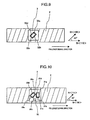
Fig. 10 is a view showing a modified example of the strain detecting portion of the load sensor in accordance with the present invention; -
Fig. 11 is a view showing a modified example of the strain detecting portion of the load sensor in accordance with the present invention; -
Fig. 12 is a view showing a transverse cross sectional structure of a major portion of a load sensor in accordance with a fifth embodiment of the present invention; -
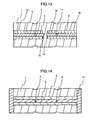
Fig. 13 is a view showing a modified example of the transverse cross sectional structure of the major portion of the load sensor in accordance with the fifth embodiment of the present invention; -
Fig. 14 is a view showing a modified example of the vertical cross sectional structure of the major portion of the load sensor in accordance with the first embodiment of the present invention; -
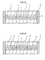
Fig. 15 is a view showing a modified example of the vertical cross sectional structure of the major portion of the load sensor in accordance with the first embodiment of the present invention; -
Fig. 16 is a view showing a modified example of the vertical cross sectional structure of the major portion of the load sensor in accordance with the first embodiment of the present invention; -
Fig. 17 is a view showing a modified example of the vertical cross sectional structure of the major portion of the load sensor in accordance with the first embodiment of the present invention; -
Fig. 18 is a view showing a load applying direction of the load sensor in accordance with the present invention; -
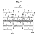
Fig. 19 is a view showing an applying method in the case that the load sensor in accordance with the present invention is applied to a shovel; -
Fig. 20 is a view showing a wiring diagram of two semiconductor strain sensors; and -
Fig. 21 is a view showing a modified example of the vertical cross sectional structure of the major portion of the load sensor in accordance with the first embodiment of the present invention. - A description will be given below of embodiments in accordance with the present invention with reference to the accompanying drawings.
- First, a description will be given of a first embodiment in the present invention with reference to
Figs. 1 and 2 . -
Figs. 1 and 2 respectively show a vertical cross sectional structure and a transverse cross sectional structure of a load sensor in accordance with the present embodiment. In the load sensor in accordance with the present embodiment shown inFigs. 1 and 2 , ahole 1a is provided near a center of apin 1, and adetection rod 2 for detecting a strain is provided in an inner portion of thehole 1a via ashock relaxation material 5. Thedetection rod 2 is provided withsemiconductor strain sensors - In this case, the
detection rod 2 is arranged near aneutral axis 100 of thepin 1, and a longitudinal direction of thedetection rod 2 is in parallel to a longitudinal direction of thepin 1. InFigs. 1 and 2 , the description is given of a case that a cross sectional shape of thedetection rod 2 is a flat plate shape, however, thedetection rod 2 may be formed as a rectangular columnar shape or a circular columnar shape. - Further, Young's modulus of a material of the
shock relaxation material 5 forming the shock relaxation layer of thepin 1 is lower than Young's modulus of a material of thepin 1 and thedetection rod 2. For example, this structure can be achieved by setting the material of theshock relaxation material 5 to an epoxy resin, setting the material of thepin 1 and thedetection rod 2 to a metal. - In this case, a measurement error caused by a heat strain is suppressed by making the
detection rod 2 by the same material as that of thepin 1. - Further, the
semiconductor strain sensors - An enlarged view of a strain detection portion in the present embodiment is shown in
Fig. 7 . Thesemiconductor strain sensor 3 is provided at a desired position of thestrain detection rod 2. Further, thesemiconductor strain sensor 3 is constituted by a silicon single crystal substrate, and fourdiffusion layers Fig. 7 . The bridge circuit is formed by these four diffusion layers. - In this case, four
diffusion layers semiconductor strain sensors - Next, a description will be given of an operation and an effect in accordance with the present embodiment.
- In accordance with the load sensor of the present embodiment, since the load applied to the
pin 1 is applied to thedetection rod 2 via theshock relaxation material 5, it is possible to relax the strain generated in the detection rod than the strain generated in the inner wall of thepin 1. Even in the case that an excessive strain is generated in thepin 1 such as a case that the shock load is applied or the like, it is possible to achieve a pin type load sensor having a high reliability without breaking the semiconductor strain sensor. - In the load sensor in accordance with the present embodiment, since the stress applied to the
pin 1 is relaxed by theshock relaxation material 5 so as to be transmitted to thedetection rod 2, and thedetection rod 2 is deformed in the same degree as thepin 1, thesemiconductor strain sensors detection rod 2. This makes use of the structure in which thedetection rod 2 has the longitudinal direction in the same direction as the longitudinal direction (an axial direction) of thepin 1 and thedetection rod 2 is deformed in the same manner as thepin 1. Further, since the stress is relaxed by theshock relaxation material 5, the stress applied to the strain sensor is small, and it is possible to prevent the strain sensor from being broken. - In the case that the strain sensor is provided in the inner wall of the hole of the
pin 1 such as the conventional structure, there can be considered to provide the shock relaxation material between the inner wall of thepin 1 and the strain sensor, however, a thickness of the shock relaxation material is limited, and it is impossible to enlarge an effect of the shock relaxation. Further, if thesemiconductor strain sensors shock relaxation material 5 without setting the detection rod, the stress applied to thesemiconductor strain sensors - Further, it is possible to suppress a bending deformation of the
detection rod 2 even in the case that a bending deformation is generated in the pin, by arranging thedetection rod 2 near the neutral axis of thepin 1, and it is possible to suppress the measurement error of thesemiconductor strain sensors detection rod 2 from being generated. - Further, it is possible to easily generate the same deformation as the deformation generated in the pin in the
detection rod 2, by setting the longitudinal direction of thedetection rod 2 in parallel to the longitudinal direction of thepin 1. - Further, it is possible to effectively relax the strain generated in the
detection rod 2 by setting the Young's modulus of the material of theshock relaxation material 5 lower to the Young's modulus of the material of thedetection rod 2. - Further, if the material of the
shock relaxation material 5 is set to the epoxy resin, it is possible to fill the liquid epoxy resin in a gap of the hole, and thereafter harden. Accordingly, there can be obtained an effect that a manufacturing method is easy and a cost can be lowered. - Further, since a rigidity of the
detection rod 2 becomes small by forming the cross sectional shape of thedetection rod 2 as the flat plate shape, the strain tends to be generated, so that this shape is effective in the case of the pin type load sensor detecting a small load. - Further, since the semiconductor strain sensor is structured such that the diffusion layers are formed on the surface of the silicon substrate, and the bridge circuit constituted by four diffusion layers is constructed on the same substrate surface, it is easy to suppress a temperature drift. Further, since the bridge circuit is constructed by one chip, it is sufficient to install only one strain sensor in the detection rod. Accordingly, since it is not necessary to align the resistances constructing the bridge circuit, there can be obtained an effect that it is easy to manufacture, and a cost can be reduced on the basis of a shortening of a manufacturing time.
- Further, since the diffusion layer formed on the surface of the silicone substrate is constituted by the P type diffusion layer, and the bridge circuit is constructed by two diffusion layers in which the longitudinal direction of the P type diffusion layer is in parallel to the direction <110> of the silicon single crystal, and two P type diffusion layers which are perpendicular thereto, there is obtained an effect that a sensitivity of the
semiconductor strain sensors - In this case, a description will be given of one example of a load detecting method by the pin type load sensor with reference to
Figs. 17 and 18 . A shear load is applied to the pin type load sensor from a vertical direction to the longitudinal direction of thepin 1. Specifically, loads 64 and 66 having the same direction are applied to supportsurfaces pin 1, and aload 65 having an opposite direction to theloads application surface 62. Accordingly, a shear deformation is generated inregions pin 1. In other words, in the case that thepin 1 is exposed to the shear load, the shear deformation is generated in thedetection rod 2 provided in the inner portion of thepin 1. - In the case that the shear deformation is generated as mentioned above, a compression strain and a tensile strain are respectively generated in two orthogonal shafts in directions which are at 45 degree with respect to the longitudinal direction of the pin. It is possible to detect these strains by the
semiconductor strain sensors - Accordingly, since the direction <110> of the silicon single crystal of the
semiconductor strain sensors Fig. 7 , it is possible to detect the shear strain generated in thepin 1 at a higher sensitivity. In other words, in the case that the shear strain caused by the shear deformation is generated in the longitudinal direction of thepin 1, a vertical strain component in the direction of 45 degree with respect to the longitudinal direction comes to a two-axis strain field in which the tensile strain is generated in one direction (a direction x), and the compression strain is generated in the vertical direction thereto (a direction y), and the vertical strain becomes maximum. - In the case that the bridge circuit is constructed by two diffusion layers in which the longitudinal direction is in parallel to the direction <110> of the silicon single crystal (Si<110>), and two P type diffusion layers which are vertical thereto, there is a feature that a strain sensitivity in parallel and vertical directions to the direction <110> is great in the both, and a code of the strain sensitivity is inverted. Accordingly, there is an advantage that it is possible to detect the shear strain at a higher sensitivity by arranging the P type diffusion layer which is parallel and vertical to the direction <110> of the silicon single crystal, in parallel to the longitudinal direction and the directions x and y in which the vertical strain becomes maximum.
- In this case,
Fig. 7 shows the case that each of the lines of the outer shape of the semiconductor silicon substrate is in parallel to the direction <100> of the silicon single crystal (Si<100>), however, the semiconductor strain sensor may be structured, as shown inFig. 8 , such that each of the lines of the outer shape is in parallel to the direction <110> of the silicon single crystal (Si<110>). - Further, in the present embodiment, there is shown the
semiconductor strain sensors semiconductor strain sensors semiconductor strain sensors pin 1, as shown inFig. 9 . In this case, it is desirable to arrange the direction <100> of the silicon single crystal of the semiconductor strain sensor in parallel to the direction which is at 45 degree with respect to the longitudinal direction of the pin. Accordingly, it is possible to detect the shear deformation of thedetection rod 2 caused by the load applied to the pin, at a high sensitivity. - In this case, as shown in
Figs. 7 and 8 , in the diffusion layer of the semiconductor strain sensor, the bridge circuit is manufactured by the P type diffusion layer which is vertical and parallel to the direction <110> of the silicon single crystal, whereby there is an advantage that the sensitivity with respect to the strain in the surface outside direction becomes approximately zero, it is easy to detect only the strain of the detection rod, and the measurement error becomes small. - Further, as shown in
Fig. 10 , two bridge circuits may be provided in thesemiconductor strain sensor 3 provided in thedetection rod 2. In other words, there are provided a bridge circuit formed by twodiffusion layers bridge circuits bridge circuits - Further, it is possible to correct an output fluctuation caused by the temperature in the case that the present load sensor is used under an environment that the temperature is changed, by providing a
temperature sensor 50, for example, by a P-N junction, on the same substrate of thesemiconductor strain sensor 3, whereby it is possible to more accurately detect the load. - In this case, as shown in
Figs. 7 and 8 , in the diffusion layer of the semiconductor strain sensor, since the bridge circuit is manufactured by the P type diffusion layer which is vertical and parallel to the direction <110> of the silicon single crystal, the sensitivity with respect to the strain in the surface outside direction becomes approximately zero, so that there is an advantage that it becomes easy to detect only the strain of the detection rod, and the measurement error becomes small. - Further, as shown in
Fig. 10 , two bridge circuits may be provided in thesemiconductor sensor 3 provided in thedetection rod 2. In other words, there are provided the bridge circuit formed by twodiffusion layers bridge circuits bridge circuits - Further, it is possible to correct the output fluctuation caused by the temperature in the case that the present load sensor is used under the environment that the temperature is changed, by providing the
temperature sensor 50, for example, by the P-N junction, on the same substrate of thesemiconductor strain sensor 3, whereby it is possible to more accurately detect the load. - In this case, in
Fig. 10 , there is shown the case that the semiconductor strain sensor is arranged in such a manner that the direction Si<100> is in parallel to the longitudinal direction of the pin, however, the semiconductor strain sensor may be arranged in such a manner that the direction Si<110> becomes in parallel to the longitudinal direction of the pin, by rotating the stain sensor at 45 degree. In this case, it is possible to detect the shear deformation of the detection rod by thebridge circuits bridge circuits - Further, as shown in
Fig. 11 ,amplifiers semiconductor strain sensor 3 provided in thedetection rod 2. Although being not always necessary, a noise resistance is improved by detecting the output of the sensor in a state of amplifying by the nearest amplifier. Further, since there is no fear that the structure of the load sensor is complicated by providing the amplifier on the same substrate, and the output is immediately amplified, there is an advantage that the noise resistance is further improved. - In this case, in
Fig. 11 , since there is shown the case that two bridge circuits are provided on thesemiconductor strain sensor 3, two amplifiers are provided, however, one amplifier may be provided per one bridge circuit. - In this case, in the present embodiment, the support surfaces 61 and 63 and the
application surface 62 are defined as shown inFig. 18 , however, the same effect can be obtained even in the case that the support surface and the application surface are exchanged. Thesemiconductor strain sensors regions - Further, a boundary between the support surfaces 61 and 63 and the
application surface 62 becomes definite by providing the outerperipheral grooves regions pin 1 is inverted, whereby it is possible to stably generate the shear deformation of thedetection rod 2, and it is possible to detect the load at the high precision. - For example, in the case that the present load sensor is applied to a shovel, it is possible to detect an applied load of a bucket of the shovel by means of the present load sensor, by connecting the portion of the support surfaces 61 and 63 to the bucket, and connecting the portion of the
load surface 62 to an arm, as shown inFig. 19 . - In this case, the load sensor in the present embodiment shown in
Fig. 1 is shown in a major part, and may be provided with acover 11 in a side surface of the load sensor as shown inFig. 14 . For example, a cover made of a metal may be provided by a bolt fastening or the like. Accordingly, it is possible to inhibit a water content or the like from making an intrusion and it is possible to inhibit the shock relaxation material from being deteriorated. - Further, as shown in
Fig. 15 , it is possible to easily position thedetection rod 2 by forming thegroove 11a in such a manner as to come into contact with the inner side of the cover provided in the side surface of the load sensor, that is, the detection rod side. In other words, it is possible to easily position thedetection rod 2 in the neutral axis of the pin by providing thegroove 11a near the center of the cover, that is, near a crossing point to the neutral axis of thepin 1. - Further, it is not necessary to provide the
shock relaxation material 5 provided in the inner portion of the pin wholly in thehole 1a of the pin, but theshock relaxation material 5 may be provided at least in theregions pin 1, theshock relaxation material 5 is provided in a part of the inner portion of thehole 1a of thepin 1, and the other portions may be formed as a cavity. In this case, there can be obtained an effect of preventing a deterioration of theshock relaxation material 5, by filling aninert gas 12. - Further, as shown in
Fig. 17 , theshock relaxation material 5 may be provided at least in theregions pin 1, and the othersolid material 13 may be filled in the other portions. - Since it is possible to prevent the water content from making an intrusion into the shock relaxation layer by employing a drying agent such as a silica gel, or a material having a waterproofing effect such as a silicon rubber or the like, as the
solid material 13, there is an advantage that it is possible to improve a reliability of the load sensor. - Further, it is not necessary that the
hole 1a of the pin provided in thepin 1 passes through the pin, but thehole 1a may be provided in such a manner as to pass at least through theregions pin 1. Since thehole 1a of the pin is provided from one side as shown inFig. 21 , there is an advantage that theshock relaxation material 5 is easily filled. Further, there is an advantage that it is possible to inhibit the water content from making an intrusion into the shock relaxation layer. - In this case, in the present embodiment shown in
Figs. 1 and 2 , there is shown the case that twosemiconductor strain sensors detection rod 2, however, it is possible to detect the load by at least one semiconductor strain sensor. However, it is possible to calculate the load from an average of the outputs by setting twosemiconductor strain sensors - Next, a description will be given of a second embodiment in the present invention with reference to
Fig. 3. Fig. 3 shows a modified example of a transverse cross sectional structure of the load sensor in accordance with the first embodiment, and the same reference numerals are attached to the common portions as the first embodiment. - The
detection rod 2 of the load sensor in accordance with the first embodiment shown inFig. 2 is formed as the flat plate shape, however, in the load sensor inFig. 3 , a detection rod 6 of a load sensor in accordance with the present embodiment is formed as a rectangular columnar shape. Further, a cross sectional shape of the detection rod 6 is a square rectangular columnar shape, and thesemiconductor strain sensors - Further, since the structure of the pin becomes isotropic with respect to two load detecting directions, by setting the cross sectional shape of the detection rod to the square shape, there is an advantage that the sensitivity with respect to the load become uniform.
- Further, in the case that the detection rod is provided with two semiconductor strain sensors, it is preferable to have a power supply line of these two semiconductor strain sensors in common in the inner portion of the pin.
- In other words, as shown in a wiring diagram of
Fig. 20 , the bridge circuit constituted by thediffusion layers semiconductor strain sensor 3 is electrically connected to the bridge circuit constituted bydiffusion layers semiconductor strain sensor 7 bywirings inner portion 43. Further, thewirings power supply lines - Next, a description will be given of a third embodiment in the present invention with reference to
Figs. 4 and5 .Figs. 4 and5 show a modified example of a transverse cross sectional structure of the load sensor in accordance with the second embodiment, and the same reference numerals are attached to the common portions as the second embodiment. - The detection rod 6 of the load sensor in accordance with the second embodiment shown in
Fig. 3 is formed as the rectangular columnar shape, and twosemiconductor strain sensors Figs. 4 and5 in accordance with the present embodiment, thesemiconductor strain sensors detection rods detection rods -
Fig. 4 shows an example in which twodetection rods Fig. 5 shows an example in which the detection rods are provided as a T-shaped form at right angles. In this case, it is preferable to arrange thesedetection rods - In the case that the detection rod is formed as the flat plate shape, and two detection rods are combined, such as the present embodiment shown in
Figs. 4 and5 , the rigidity of the detection rod becomes small in comparison with the rectangular column. Accordingly, the strain tends to be generated, and this structure is effective in the case of the pin type load sensor detecting the small load. - In this case, in the present embodiment, the description is given of the case that the
detection rods detection rods detection rods - Next, a description will be given of a fourth embodiment in the present invention with reference to
Fig. 6. Fig. 6 shows a modified example of the transverse cross section structure of the load sensor in accordance with the second embodiment, and the same reference numerals are attached to the common portions as the second embodiment. - In the load sensor in
Fig. 6 , the detection rod 6 of the load sensor in accordance with the second embodiment shown inFig. 3 is formed as a rectangular columnar shape, and twosemiconductor strain sensors detection rod 14 is formed as a circular columnar shape, and twosemiconductor strain sensors flat surface portion 14a is provided near a portion provided with the semiconductor strain sensor. Theflat surface portion 14a is not always necessary, however, there is an advantage that the semiconductor strain sensor is easily provided in thedetection rod 14, and a peeling is suppressed. - As shown in the present embodiment, there is an advantage that an isotropic structure is formed with respect to an outer peripheral direction of the pin by forming the detection rod as the columnar shape, and a precision of measurement can be improved.
- Next, a description will be given of a fifth embodiment in the present invention with reference to
Fig. 12. Fig. 12 shows a modified example of the vertical cross sectional structure of the load sensor in accordance with the first embodiment, and the same reference numerals are attached to the common portions as the first embodiment. - In the load sensor in accordance with the first embodiment shown in
Fig. 1 , only onehole 1a is provided in thepin 1, however, in a load sensor shown inFig. 12 , twoholes pin 1, and thedetection rods semiconductor strain sensors detection rods - As shown in the present embodiment, since a depth of the hole can be made shallow by providing the
holes pin 1, there is an advantage that it is easy to work. - Further, there is an advantage that it is easy to arrange the
detection rods pin 1 by providingshallow grooves holes Fig. 13 . - As mentioned above, in accordance with the load sensors on the basis of the present invention shown in the first to fifth embodiments, since the structure of the detection rod is simple, and the manufacturing method can be simplified, there is an advantage that the pin type load sensor can be inexpensively manufactured. Further, since the semiconductor strain sensor having the high strain sensitivity is used as the strain measuring apparatus, there is an advantage that it is not necessary to amplify the signal by the amplifier or the like, and it is possible to lower a cost as a whole of the load sensor system. Further, in the case of the load sensor utilizing the strain gauge, there is the problem that the wiring from the strain gauge to the amplifier tends to be affected by the noise and the SN ratio is lowered, however, in the case of the semiconductor strain sensor, since the strain sensitivity is high and the output of the sensor is great, the semiconductor strain sensor is hard to be affected by the noise, and it is possible to inhibit the SN ratio from being lowered.
- It should be further understood by those skilled in the art that although the foregoing description has been made on embodiments of the invention, the invention is not limited thereto and various changes and modifications may be made without departing from the spirit of the invention and the scope of the appended claims.
Claims (17)
- A load sensor characterized by comprising:a pin (1) having a hole (1a) provided in a region including a neutral axis;a detection rod (2, 6, 8, 9, 14) provided in an inner portion of said hole;a semiconductor strain sensor (3, 4, 7) provided in said detection rod; anda shock relaxation material (5, 10) provided between said detection rod and said pin in the inner portion of said hole.
- A load sensor as claimed in claim 1, characterized in that said detection rod is provided in the region including the neutral axis of said pin.
- A load sensor as claimed in claim 1, characterized in that Young's modulus of said shock relaxation material is lower than Young's modulus of said pin and said detection rod.
- A load sensor as claimed in claim 1, characterized in that a material of said shock relaxation material is an epoxy resin
- A load sensor as claimed in claim 1, characterized in that a material of said detection rod is a metal.
- A load sensor as claimed in claim 5, characterized in that the material of said detection rod is the same as the material of said pin.
- A load sensor as claimed in claim 1, characterized in that a cross sectional shape of said detection rod is a square.
- A load sensor as claimed in claim 1, characterized in that a cross sectional shape of said detection rod is a flat plate.
- A load sensor as claimed in claim 1, characterized in that a longitudinal direction of the detection rod is in parallel to a longitudinal direction of the pin.
- A load sensor as claimed in claim 1, characterized in that said semiconductor strain sensor is provided in such a manner as to detect a shear strain of said detection rod.
- A load sensor as claimed in claim 1, characterized in that said semiconductor strain sensor is provided with a diffusion layer (30a-30d, 31a-31d, 32a-32d, 44a-44d) on a surface of a silicon substrate, and is constructed by a bridge circuit constituted by four diffusion layers on the same substrate surface.
- A load sensor as claimed in claim 11, characterized in that the diffusion layer formed on the surface of said silicon substrate is constituted by a P type diffusion layer, and the bridge circuit is constructed by two diffusion resistances in which a longitudinal direction of said P type diffusion layer is in parallel to a direction <110> of a silicon single crystal, and two P type diffusion layers which are perpendicular thereto.
- A load sensor as claimed in claim 12, characterized in that the direction <110> of the silicon single crystal of said strain sensor is arranged in parallel to a direction of 45 degree with respect to the longitudinal direction of the pin.
- A load sensor as claimed in claim 1, characterized in that the detection rod is constituted by a rectangular column having a square cross sectional shape, and the strain sensors are provided in two orthogonal surfaces of said rectangular columns.
- A load sensor as claimed in claim 13, characterized in that power supply lines of said two or more strain sensors are held in common in the inner portion of the pin, and the number of the wiring drawn out to an outer portion of the pin from said two or more strain sensors is obtained by a formula (number of sensors x 2) + 2.
- A load sensor as claimed in claim 1, characterized in that the detection rod is constituted by a circular column, and the strain sensor is provided at least on one surface of said circular column.
- A manufacturing method of a load sensor characterized in that the method comprises:a step of attaching a semiconductor strain sensor (3, 4, 7) to a detection rod (2, 6, 8, 9, 14);a step of inserting the detection rod attaching said semiconductor strain sensor thereto into a hole (1a) provided in a region including a center shaft of a pin (1); anda step of filling a resin in the hole of said pin so as to form a shock relaxation material (5, 10).
Applications Claiming Priority (1)
| Application Number | Priority Date | Filing Date | Title |
|---|---|---|---|
| JP2007202454A JP4528810B2 (en) | 2007-08-03 | 2007-08-03 | Load sensor and load sensor manufacturing method |
Publications (3)
| Publication Number | Publication Date |
|---|---|
| EP2023109A2 true EP2023109A2 (en) | 2009-02-11 |
| EP2023109A3 EP2023109A3 (en) | 2010-11-24 |
| EP2023109B1 EP2023109B1 (en) | 2016-07-20 |
Family
ID=39926685
Family Applications (1)
| Application Number | Title | Priority Date | Filing Date |
|---|---|---|---|
| EP08013877.9A Not-in-force EP2023109B1 (en) | 2007-08-03 | 2008-08-01 | Load sensor with semiconductive strain gauges |
Country Status (3)
| Country | Link |
|---|---|
| US (1) | US7793551B2 (en) |
| EP (1) | EP2023109B1 (en) |
| JP (1) | JP4528810B2 (en) |
Families Citing this family (17)
| Publication number | Priority date | Publication date | Assignee | Title |
|---|---|---|---|---|
| WO2008086283A2 (en) * | 2007-01-08 | 2008-07-17 | Precision Planting Inc. | Load sensing pin |
| JP5427733B2 (en) * | 2010-08-27 | 2014-02-26 | 株式会社日立製作所 | Mechanical quantity measuring device |
| US8788155B2 (en) * | 2012-07-16 | 2014-07-22 | Flanders Electric Motor Service, Inc. | Optimized bank penetration system |
| US9016134B2 (en) * | 2012-12-11 | 2015-04-28 | Goodrich Corporation | Circular load cell strain sensor configuration |
| JP6110242B2 (en) * | 2013-07-09 | 2017-04-05 | 日立建機株式会社 | Load detection apparatus and work machine equipped with the same |
| WO2015047360A1 (en) * | 2013-09-29 | 2015-04-02 | Rinand Solutions Llc | Force sensing compliant enclosure |
| US10000249B2 (en) * | 2014-08-22 | 2018-06-19 | Shimano Inc. | Bicycle pedal |
| US20160157729A1 (en) * | 2014-12-09 | 2016-06-09 | Canon Kabushiki Kaisha | Acoustic imaging apparatus |
| WO2016163194A1 (en) * | 2015-04-06 | 2016-10-13 | 株式会社日立製作所 | External force measurement system for work machine and work machine |
| US10402616B2 (en) * | 2015-10-21 | 2019-09-03 | Motorola Mobility Llc | Fingerprint sensor with proximity detection, and corresponding devices, systems, and methods |
| CN106017918A (en) * | 2016-06-14 | 2016-10-12 | 广东精铟海洋工程股份有限公司 | Marine engineering lifting platform rack load measuring device |
| CN105865672A (en) * | 2016-06-14 | 2016-08-17 | 广东精铟海洋工程股份有限公司 | High-sensitivity rack load measuring device based on radial through hole |
| US10323992B2 (en) * | 2016-09-26 | 2019-06-18 | Tecsis Gmbh | Force measuring load pin having at least one sensor and a slot that divides the load pin into upper and lower portions |
| IT201800003693A1 (en) * | 2018-03-16 | 2019-09-16 | St Microelectronics Srl | STRESS SENSOR, STRUCTURAL INTEGRITY MONITORING SYSTEM FOR CONSTRUCTION AND MANUFACTURING PROCESS OF A STRESS SENSOR |
| JP7369455B2 (en) * | 2018-05-24 | 2023-10-26 | 国立大学法人東海国立大学機構 | Living body occupancy detection device |
| JP2019215267A (en) * | 2018-06-13 | 2019-12-19 | 宮地エンジニアリング株式会社 | Support reaction calculation method of beam structure, and support reaction management system of beam structure |
| JP7260094B2 (en) * | 2019-05-22 | 2023-04-18 | ユニパルス株式会社 | Load converter and cargo handling assistance device using the same |
Citations (4)
| Publication number | Priority date | Publication date | Assignee | Title |
|---|---|---|---|---|
| GB1473170A (en) | 1974-07-25 | 1977-05-11 | ||
| US4864874A (en) | 1987-08-05 | 1989-09-12 | Pfister Gmbh | Force measuring device |
| JPH1038713A (en) | 1996-07-17 | 1998-02-13 | Minebea Co Ltd | Pin type load cell |
| JP2005114443A (en) | 2003-10-06 | 2005-04-28 | Hitachi Ltd | Mechanical quantity measuring device |
Family Cites Families (21)
| Publication number | Priority date | Publication date | Assignee | Title |
|---|---|---|---|---|
| DE2117424A1 (en) * | 1971-04-08 | 1972-10-12 | Pietzsch Ludwig | Load cell |
| US4389896A (en) * | 1981-05-27 | 1983-06-28 | The United States Of America As Represented By The Secretary Of The Interior | Borehole gauge for in-situ measurement of stress and other physical properties |
| US4429579A (en) * | 1981-10-26 | 1984-02-07 | Helm Instrument Co., Inc. | Tie rod tension sensor |
| EP0126172B1 (en) * | 1983-05-20 | 1987-04-08 | Hottinger Baldwin Messtechnik Gmbh | Damping means for force tranducers |
| US4804053B1 (en) * | 1987-11-10 | 1996-09-03 | Flintab Ab | Rocker pin load cell |
| US4894938A (en) * | 1989-05-30 | 1990-01-23 | The United States Of America As Represented By The Secretary Of The Army | Firing pin force transducer |
| JPH04329328A (en) * | 1991-05-02 | 1992-11-18 | Fuji Electric Co Ltd | Contact pressure sensor and its measurement method |
| US5147213A (en) * | 1991-10-24 | 1992-09-15 | Minnesota Mining And Manufacturing Company | Zero insertion pressure test socket for pin grid array electronic packages |
| DE4214291A1 (en) * | 1992-04-30 | 1993-11-04 | Pfister Messtechnik | FORCE MEASURING DEVICE |
| JPH0669758U (en) * | 1993-03-04 | 1994-09-30 | 矢崎総業株式会社 | Sensing element for vehicle load measuring device |
| JP3433439B2 (en) * | 1996-06-26 | 2003-08-04 | 長野計器株式会社 | Sensing element |
| JP3937525B2 (en) * | 1997-09-10 | 2007-06-27 | 双葉電子工業株式会社 | Ejector pin with pressure sensor |
| US6913581B2 (en) * | 2000-03-20 | 2005-07-05 | Paul D. Corl | High output therapeutic ultrasound transducer |
| US6508775B2 (en) * | 2000-03-20 | 2003-01-21 | Pharmasonics, Inc. | High output therapeutic ultrasound transducer |
| US6605006B2 (en) * | 2000-07-05 | 2003-08-12 | Milton T. Mason | Golf club |
| US6446510B1 (en) * | 2000-07-24 | 2002-09-10 | Kulite Semiconductor Products, Inc. | Force transducer assembly |
| US6951137B2 (en) * | 2001-07-02 | 2005-10-04 | Alliant Techsystems, Inc. | Method and apparatus for measuring bending in a pin member |
| US7430920B2 (en) * | 2005-12-16 | 2008-10-07 | Hitachi, Ltd. | Apparatus for measuring a mechanical quantity |
| JP2006220574A (en) * | 2005-02-14 | 2006-08-24 | Hitachi Ltd | Rotor dynamic quantity measuring device and rotary dynamic quantity measuring system |
| JP2007255953A (en) | 2006-03-22 | 2007-10-04 | Hitachi Ltd | Mechanical quantity measuring device |
| JP4697004B2 (en) | 2006-03-29 | 2011-06-08 | 株式会社日立製作所 | Mechanical quantity measuring device |
-
2007
- 2007-08-03 JP JP2007202454A patent/JP4528810B2/en not_active Expired - Fee Related
-
2008
- 2008-08-01 EP EP08013877.9A patent/EP2023109B1/en not_active Not-in-force
- 2008-08-01 US US12/184,426 patent/US7793551B2/en not_active Expired - Fee Related
Patent Citations (4)
| Publication number | Priority date | Publication date | Assignee | Title |
|---|---|---|---|---|
| GB1473170A (en) | 1974-07-25 | 1977-05-11 | ||
| US4864874A (en) | 1987-08-05 | 1989-09-12 | Pfister Gmbh | Force measuring device |
| JPH1038713A (en) | 1996-07-17 | 1998-02-13 | Minebea Co Ltd | Pin type load cell |
| JP2005114443A (en) | 2003-10-06 | 2005-04-28 | Hitachi Ltd | Mechanical quantity measuring device |
Also Published As
| Publication number | Publication date |
|---|---|
| US7793551B2 (en) | 2010-09-14 |
| JP4528810B2 (en) | 2010-08-25 |
| EP2023109A3 (en) | 2010-11-24 |
| US20090031819A1 (en) | 2009-02-05 |
| EP2023109B1 (en) | 2016-07-20 |
| JP2009036686A (en) | 2009-02-19 |
Similar Documents
| Publication | Publication Date | Title |
|---|---|---|
| EP2023109B1 (en) | Load sensor with semiconductive strain gauges | |
| JP4617943B2 (en) | Mechanical quantity measuring device | |
| US8659101B2 (en) | Physical quantity detector | |
| US11137299B2 (en) | Multi-axial force sensor including piezoresistive groups, method of manufacturing the multi-axial force sensor, and method for operating the multi-axial force sensor | |
| US9441941B2 (en) | Deformation measurement sensor for measuring pressure and shearing force and structure therefor | |
| EP3534126B1 (en) | Sensing device, in particular load sensing device | |
| JP2007255953A (en) | Mechanical quantity measuring device | |
| US9983084B2 (en) | Pressure sensing assembly for structural health monitoring systems | |
| US20090266170A1 (en) | Pressure sensor, manufacturing method thereof, and electronic component provided therewith | |
| US11320324B2 (en) | Sensor device | |
| US20220120633A1 (en) | Stress sensor, structural health monitoring system for constructions and process for manufacturing a stress sensor | |
| JP2002236064A (en) | Bolt with strain sensor and strain sensor | |
| US10737929B2 (en) | Trench-based microelectromechanical transducer and method for manufacturing the microelectromechanical transducer | |
| JP2012122924A (en) | Pressure sensor | |
| JP2006098321A (en) | Semiconductor-type three-axis acceleration sensor | |
| US10392923B2 (en) | System and methodology for determining forces acting on components | |
| US6840111B2 (en) | Micromechanical component and pressure sensor having a component of this type | |
| JP5149081B2 (en) | Fastener with strain measurement function | |
| US9506823B2 (en) | Bonding stress testing arrangement and method of determining stress | |
| Divay et al. | Highly sensitive force sensor featuring a MEMS-instrumented buckling lamella | |
| Azevedo et al. | Influence of sensor substrate geometry on the sensitivity of mems micro-extensometers | |
| JP5265216B2 (en) | Pin type load cell | |
| RU2404415C1 (en) | Sensor for measuring longitudinal forces | |
| JP2008008694A (en) | Strain measuring device | |
| Chaparala et al. | A new technique for calibrating piezoresistive stress sensor chips |
Legal Events
| Date | Code | Title | Description |
|---|---|---|---|
| PUAI | Public reference made under article 153(3) epc to a published international application that has entered the european phase |
Free format text: ORIGINAL CODE: 0009012 |
|
| 17P | Request for examination filed |
Effective date: 20080801 |
|
| AK | Designated contracting states |
Kind code of ref document: A2 Designated state(s): AT BE BG CH CY CZ DE DK EE ES FI FR GB GR HR HU IE IS IT LI LT LU LV MC MT NL NO PL PT RO SE SI SK TR |
|
| AX | Request for extension of the european patent |
Extension state: AL BA MK RS |
|
| PUAL | Search report despatched |
Free format text: ORIGINAL CODE: 0009013 |
|
| AK | Designated contracting states |
Kind code of ref document: A3 Designated state(s): AT BE BG CH CY CZ DE DK EE ES FI FR GB GR HR HU IE IS IT LI LT LU LV MC MT NL NO PL PT RO SE SI SK TR |
|
| AX | Request for extension of the european patent |
Extension state: AL BA MK RS |
|
| AKX | Designation fees paid |
Designated state(s): DE FR GB IT SE |
|
| 17Q | First examination report despatched |
Effective date: 20110715 |
|
| REG | Reference to a national code |
Ref country code: DE Ref legal event code: R079 Ref document number: 602008045161 Country of ref document: DE Free format text: PREVIOUS MAIN CLASS: G01L0001180000 Ipc: G01L0001220000 |
|
| GRAJ | Information related to disapproval of communication of intention to grant by the applicant or resumption of examination proceedings by the epo deleted |
Free format text: ORIGINAL CODE: EPIDOSDIGR1 |
|
| GRAP | Despatch of communication of intention to grant a patent |
Free format text: ORIGINAL CODE: EPIDOSNIGR1 |
|
| RIC1 | Information provided on ipc code assigned before grant |
Ipc: G01L 1/26 20060101ALI20150618BHEP Ipc: G01L 5/16 20060101ALI20150618BHEP Ipc: G01L 1/22 20060101AFI20150618BHEP Ipc: G01L 1/18 20060101ALI20150618BHEP |
|
| INTG | Intention to grant announced |
Effective date: 20150720 |
|
| GRAS | Grant fee paid |
Free format text: ORIGINAL CODE: EPIDOSNIGR3 |
|
| GRAJ | Information related to disapproval of communication of intention to grant by the applicant or resumption of examination proceedings by the epo deleted |
Free format text: ORIGINAL CODE: EPIDOSDIGR1 |
|
| GRAP | Despatch of communication of intention to grant a patent |
Free format text: ORIGINAL CODE: EPIDOSNIGR1 |
|
| INTG | Intention to grant announced |
Effective date: 20160104 |
|
| GRAS | Grant fee paid |
Free format text: ORIGINAL CODE: EPIDOSNIGR3 |
|
| GRAA | (expected) grant |
Free format text: ORIGINAL CODE: 0009210 |
|
| RIN1 | Information on inventor provided before grant (corrected) |
Inventor name: SHIMODAIRA, TAKAYUKI Inventor name: SHIMAZU, HIROMI Inventor name: TANNO, YOHEI Inventor name: TAKADA, RYUJI Inventor name: OHTA, HIROYUKI |
|
| AK | Designated contracting states |
Kind code of ref document: B1 Designated state(s): DE FR GB IT SE |
|
| REG | Reference to a national code |
Ref country code: GB Ref legal event code: FG4D |
|
| RIN1 | Information on inventor provided before grant (corrected) |
Inventor name: SHIMAZU, HIROMI Inventor name: OHTA, HIROYUKI Inventor name: TANNO, YOHEI Inventor name: SHIMODAIRA, TAKAYUKI Inventor name: TAKADA, RYUJI |
|
| REG | Reference to a national code |
Ref country code: DE Ref legal event code: R096 Ref document number: 602008045161 Country of ref document: DE |
|
| PG25 | Lapsed in a contracting state [announced via postgrant information from national office to epo] |
Ref country code: IT Free format text: LAPSE BECAUSE OF FAILURE TO SUBMIT A TRANSLATION OF THE DESCRIPTION OR TO PAY THE FEE WITHIN THE PRESCRIBED TIME-LIMIT Effective date: 20160720 |
|
| PG25 | Lapsed in a contracting state [announced via postgrant information from national office to epo] |
Ref country code: SE Free format text: LAPSE BECAUSE OF FAILURE TO SUBMIT A TRANSLATION OF THE DESCRIPTION OR TO PAY THE FEE WITHIN THE PRESCRIBED TIME-LIMIT Effective date: 20160720 |
|
| REG | Reference to a national code |
Ref country code: DE Ref legal event code: R097 Ref document number: 602008045161 Country of ref document: DE |
|
| PLBE | No opposition filed within time limit |
Free format text: ORIGINAL CODE: 0009261 |
|
| REG | Reference to a national code |
Ref country code: FR Ref legal event code: ST Effective date: 20170428 |
|
| STAA | Information on the status of an ep patent application or granted ep patent |
Free format text: STATUS: NO OPPOSITION FILED WITHIN TIME LIMIT |
|
| 26N | No opposition filed |
Effective date: 20170421 |
|
| PG25 | Lapsed in a contracting state [announced via postgrant information from national office to epo] |
Ref country code: FR Free format text: LAPSE BECAUSE OF NON-PAYMENT OF DUE FEES Effective date: 20160920 |
|
| PGFP | Annual fee paid to national office [announced via postgrant information from national office to epo] |
Ref country code: DE Payment date: 20180717 Year of fee payment: 11 |
|
| PGFP | Annual fee paid to national office [announced via postgrant information from national office to epo] |
Ref country code: GB Payment date: 20180801 Year of fee payment: 11 |
|
| REG | Reference to a national code |
Ref country code: DE Ref legal event code: R119 Ref document number: 602008045161 Country of ref document: DE |
|
| GBPC | Gb: european patent ceased through non-payment of renewal fee |
Effective date: 20190801 |
|
| PG25 | Lapsed in a contracting state [announced via postgrant information from national office to epo] |
Ref country code: DE Free format text: LAPSE BECAUSE OF NON-PAYMENT OF DUE FEES Effective date: 20200303 |
|
| PG25 | Lapsed in a contracting state [announced via postgrant information from national office to epo] |
Ref country code: GB Free format text: LAPSE BECAUSE OF NON-PAYMENT OF DUE FEES Effective date: 20190801 |