EP2022872A1 - Thin film production equipment and inner block for thin film production equipment - Google Patents
Thin film production equipment and inner block for thin film production equipment Download PDFInfo
- Publication number
- EP2022872A1 EP2022872A1 EP07742664A EP07742664A EP2022872A1 EP 2022872 A1 EP2022872 A1 EP 2022872A1 EP 07742664 A EP07742664 A EP 07742664A EP 07742664 A EP07742664 A EP 07742664A EP 2022872 A1 EP2022872 A1 EP 2022872A1
- Authority
- EP
- European Patent Office
- Prior art keywords
- gas
- vacuum tank
- thin film
- film production
- inner block
- Prior art date
- Legal status (The legal status is an assumption and is not a legal conclusion. Google has not performed a legal analysis and makes no representation as to the accuracy of the status listed.)
- Withdrawn
Links
Images


Classifications
-
- C—CHEMISTRY; METALLURGY
- C23—COATING METALLIC MATERIAL; COATING MATERIAL WITH METALLIC MATERIAL; CHEMICAL SURFACE TREATMENT; DIFFUSION TREATMENT OF METALLIC MATERIAL; COATING BY VACUUM EVAPORATION, BY SPUTTERING, BY ION IMPLANTATION OR BY CHEMICAL VAPOUR DEPOSITION, IN GENERAL; INHIBITING CORROSION OF METALLIC MATERIAL OR INCRUSTATION IN GENERAL
- C23C—COATING METALLIC MATERIAL; COATING MATERIAL WITH METALLIC MATERIAL; SURFACE TREATMENT OF METALLIC MATERIAL BY DIFFUSION INTO THE SURFACE, BY CHEMICAL CONVERSION OR SUBSTITUTION; COATING BY VACUUM EVAPORATION, BY SPUTTERING, BY ION IMPLANTATION OR BY CHEMICAL VAPOUR DEPOSITION, IN GENERAL
- C23C16/00—Chemical coating by decomposition of gaseous compounds, without leaving reaction products of surface material in the coating, i.e. chemical vapour deposition [CVD] processes
- C23C16/44—Chemical coating by decomposition of gaseous compounds, without leaving reaction products of surface material in the coating, i.e. chemical vapour deposition [CVD] processes characterised by the method of coating
-
- C—CHEMISTRY; METALLURGY
- C23—COATING METALLIC MATERIAL; COATING MATERIAL WITH METALLIC MATERIAL; CHEMICAL SURFACE TREATMENT; DIFFUSION TREATMENT OF METALLIC MATERIAL; COATING BY VACUUM EVAPORATION, BY SPUTTERING, BY ION IMPLANTATION OR BY CHEMICAL VAPOUR DEPOSITION, IN GENERAL; INHIBITING CORROSION OF METALLIC MATERIAL OR INCRUSTATION IN GENERAL
- C23C—COATING METALLIC MATERIAL; COATING MATERIAL WITH METALLIC MATERIAL; SURFACE TREATMENT OF METALLIC MATERIAL BY DIFFUSION INTO THE SURFACE, BY CHEMICAL CONVERSION OR SUBSTITUTION; COATING BY VACUUM EVAPORATION, BY SPUTTERING, BY ION IMPLANTATION OR BY CHEMICAL VAPOUR DEPOSITION, IN GENERAL
- C23C16/00—Chemical coating by decomposition of gaseous compounds, without leaving reaction products of surface material in the coating, i.e. chemical vapour deposition [CVD] processes
- C23C16/44—Chemical coating by decomposition of gaseous compounds, without leaving reaction products of surface material in the coating, i.e. chemical vapour deposition [CVD] processes characterised by the method of coating
- C23C16/458—Chemical coating by decomposition of gaseous compounds, without leaving reaction products of surface material in the coating, i.e. chemical vapour deposition [CVD] processes characterised by the method of coating characterised by the method used for supporting substrates in the reaction chamber
- C23C16/4582—Rigid and flat substrates, e.g. plates or discs
- C23C16/4583—Rigid and flat substrates, e.g. plates or discs the substrate being supported substantially horizontally
- C23C16/4585—Devices at or outside the perimeter of the substrate support, e.g. clamping rings, shrouds
-
- C—CHEMISTRY; METALLURGY
- C23—COATING METALLIC MATERIAL; COATING MATERIAL WITH METALLIC MATERIAL; CHEMICAL SURFACE TREATMENT; DIFFUSION TREATMENT OF METALLIC MATERIAL; COATING BY VACUUM EVAPORATION, BY SPUTTERING, BY ION IMPLANTATION OR BY CHEMICAL VAPOUR DEPOSITION, IN GENERAL; INHIBITING CORROSION OF METALLIC MATERIAL OR INCRUSTATION IN GENERAL
- C23C—COATING METALLIC MATERIAL; COATING MATERIAL WITH METALLIC MATERIAL; SURFACE TREATMENT OF METALLIC MATERIAL BY DIFFUSION INTO THE SURFACE, BY CHEMICAL CONVERSION OR SUBSTITUTION; COATING BY VACUUM EVAPORATION, BY SPUTTERING, BY ION IMPLANTATION OR BY CHEMICAL VAPOUR DEPOSITION, IN GENERAL
- C23C16/00—Chemical coating by decomposition of gaseous compounds, without leaving reaction products of surface material in the coating, i.e. chemical vapour deposition [CVD] processes
- C23C16/44—Chemical coating by decomposition of gaseous compounds, without leaving reaction products of surface material in the coating, i.e. chemical vapour deposition [CVD] processes characterised by the method of coating
- C23C16/458—Chemical coating by decomposition of gaseous compounds, without leaving reaction products of surface material in the coating, i.e. chemical vapour deposition [CVD] processes characterised by the method of coating characterised by the method used for supporting substrates in the reaction chamber
- C23C16/4582—Rigid and flat substrates, e.g. plates or discs
- C23C16/4583—Rigid and flat substrates, e.g. plates or discs the substrate being supported substantially horizontally
- C23C16/4586—Elements in the interior of the support, e.g. electrodes, heating or cooling devices
-
- C—CHEMISTRY; METALLURGY
- C23—COATING METALLIC MATERIAL; COATING MATERIAL WITH METALLIC MATERIAL; CHEMICAL SURFACE TREATMENT; DIFFUSION TREATMENT OF METALLIC MATERIAL; COATING BY VACUUM EVAPORATION, BY SPUTTERING, BY ION IMPLANTATION OR BY CHEMICAL VAPOUR DEPOSITION, IN GENERAL; INHIBITING CORROSION OF METALLIC MATERIAL OR INCRUSTATION IN GENERAL
- C23C—COATING METALLIC MATERIAL; COATING MATERIAL WITH METALLIC MATERIAL; SURFACE TREATMENT OF METALLIC MATERIAL BY DIFFUSION INTO THE SURFACE, BY CHEMICAL CONVERSION OR SUBSTITUTION; COATING BY VACUUM EVAPORATION, BY SPUTTERING, BY ION IMPLANTATION OR BY CHEMICAL VAPOUR DEPOSITION, IN GENERAL
- C23C16/00—Chemical coating by decomposition of gaseous compounds, without leaving reaction products of surface material in the coating, i.e. chemical vapour deposition [CVD] processes
- C23C16/44—Chemical coating by decomposition of gaseous compounds, without leaving reaction products of surface material in the coating, i.e. chemical vapour deposition [CVD] processes characterised by the method of coating
- C23C16/52—Controlling or regulating the coating process
Definitions
- the present invention relates to a thin film production apparatus such as an MOCVD apparatus. More specifically, the present invention relates to a thin film production apparatus and an inner block for a thin film production apparatus capable of adjusting a volume of a reaction space depending on a size of a substrate to be processed.
- Patent Document 1 Japanese Patent Application Laid-open No. 2004-35971
- one semiconductor production apparatus is constituted by a plurality of process modules, and one process module is constituted by, for example, approximately a thousand components.
- Diversification of apparatuses causes differences in structural components, which then requires as many assembly operation processes and component adjusting methods as the number of the different components, with the result that operation categories are increased in number to inhibit the assembly operations and product inspection operations, whereby the early delivery demand cannot be met.
- the increased number of component categories also increases the number of order operations, delivery date confirmation operations, and reception operations as much as the number of the components, thereby bulging purchase-related operations.
- the increased number of component categories may inhibit budget priority of bulk purchase, and, in addition, delivery of each component may lead to a failure in meeting the early delivery demand.
- the different components require different settings of processing machines and cutting tools, whereby labor hours required for changing the setting backfire on prices and delivery dates.
- the reaction space is required to be structured as small as possible in accordance with the substrate.
- various components such as piping and equipment connected to the vacuum tank are changed.
- the alteration of the mechanical components may lead to alteration of electronic components such as sensors and wirings, and the alteration of the electronic components may alter control software, which eventually leads to a large number of component categories.
- CO 2 carbon dioxide
- the present invention has been made in view of the above-mentioned problems, and it is an object of the present invention to provide a thin film production apparatus and an inner block for a thin film production apparatus that enable cost reduction and improvement of deposition efficiency by employing a common component.
- a thin film production apparatus having a vacuum tank, a lid body closing an upper portion of the vacuum tank, a stage for supporting a substrate to be processed, and a gas head mounted to the lid body such that the gas head is opposed to the stage, includes an inner block disposed between the vacuum tank and the lid body and including a built-in heating source, for determining a volume of a reaction space between the stage and the gas head.
- the volume of the reaction space is optimized by merely altering a size of the inner block without altering a size of the vacuum tank.
- the inner block is an annular block body disposed between an inner wall surface of the vacuum tank and an outer circumferential portion of the stage, and is mounted to the vacuum tank and the lid body via seal members.
- the inner block having the above structure, the volume of the reaction space can be readily optimized by merely altering an inner diameter of the block body in accordance with the substrate size.
- the inner block includes a heating source, and heat adjustment is executed to a predetermined process temperature during film formation, thereby improving gas use efficiency and deposition efficiency.
- the predetermined process temperature at least only in an area of the inner block opposed to the reaction space instead of the entire inner block, power consumption can be decreased.
- the spatial area opposed to a low temperature portion of the inner block larger in volume than the reaction space, and preferably by introducing an inert gas for controlling gas partial pressure into the spatial area, precipitation of material elements of the deposition gas onto a surface of the low temperature portion of the inner block can be suppressed.
- film formation on plural kinds of substrates having different sizes is enabled using a common vacuum tank. Further, increase of the number of apparatus structural components to be prepared for each size of the substrate to be processed can be minimized, whereby the cost of the components can be reduced, and, while simplifying assembling operation, product inspection operation, and adjusting operation, excellent deposition efficiency and stable film formation can be realized.
- Fig. 1 is a piping arrangement diagram of a deposition gas supply line and a vacuum exhaust line of a thin film production apparatus 10 according to an embodiment of the present invention.
- the "deposition gas” refers to an unmixed gas such as a material gas, a reaction gas, or an inert gas or a mixed gas thereof used in a chemical reaction.
- the thin film production apparatus 10 includes a vacuum tank 12 having a processing chamber (film formation chamber) 11 formed therein, a gas head 13 for introducing a deposition gas into the processing chamber 11, and a stage 14 disposed in the processing chamber 11, for supporting a substrate to be processed (hereinafter referred to as "substrate”) W such as a semiconductor wafer or a glass substrate.
- substrate a substrate to be processed
- the processing chamber 11 is connected via a vacuum exhaust line 25 to a vacuum exhaust apparatus 26, and is structured such that, when opening a main valve V0, the processing chamber 11 can be evacuated to a predetermined reduced-pressure atmosphere.
- the stage 14 is arranged so as to be opposed to the gas head 13.
- the stage 14 is made of, for example, a hot plate, and is capable of heating the substrate W placed on the stage 14 to a predetermined temperature.
- the gas head 13 is connected to a reaction gas supply line 21 communicating with a reaction gas source and a material gas supply line 22 communicating with a material gas source as will be described later in detail, and introduces a reaction gas and a material gas, or a mixed gas thereof into the processing chamber 11.
- the gas head 13 employs a shower head provided with plural gas ejection holes.
- reaction gas NH 3 (ammonia gas), H 2 (hydrogen gas), or the like is used.
- material gas an organic metal material including metallic species (Ta, Cu, Al, Ti, Zr, V, Nb) to be deposited is used, which is selected depending on an intended application (wiring film, barrier film, etc.).
- an activated nitride gas e.g., ammonia gas is used so that a nitride film of the above metal is formed.
- inert gas N 2 or Ar is used as the inert gas.
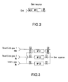
- the reaction gas source is a generally-used gas source (reaction gas source, inert gas source, etc.) whose gas flow rate can be controlled using a mass flow controller (MFC) as shown in Fig. 2 .
- One integration-type gas source can supply a plurality of gases therefrom.
- Fig. 3 exemplifies the integration-type gas source.
- a reaction gas 1 is NH 3
- a reaction gas 2 is H 2
- an inert gas is N 2 .
- Unmixed gases thereof or a mixed gas thereof can be used as a gas source.
- the material gas source there is employed a system in which a solid or liquid organic metal material is gasified to obtain a material gas.
- a vaporizing system in which a liquid is supplied to a vaporizer to be vaporized, or a bubbling system.
- a combined system of a material heating system in which a solid is heated to be liquefied and then vaporized by the vaporizer and the vaporizing system, a combined system of a heating system and the bubbling system, a sublimation system in which a solid material is gasified, or the like.
- the material gas is not limited to the organic metal material and can employ a gas such as WF 6 generally used in a semiconductor production process.
- reaction gas and the material gas introduced into the processing chamber 11 chemically-react with each other_to form a metal thin film on the substrate W.
- a by-product and a redundant gas are discharged via the vacuum exhaust line 25.
- the reaction gas and the material gas may be introduced into the film formation chamber 11 simultaneously or separately.
- the material gas supply line 22 is switched between introduction/non-introduction of_the material gas.
- the material gas can be discharged via a bypass piping 24, not via the processing chamber 11.
- the second valve V2 is closed during film formation and is opened when the film formation is finished.
- a radical source 29 for exciting the reaction gas supplied via the reaction gas supply line 21 to produce a radical gas is disposed in the vicinity of the gas head 13.
- a catalytic wire heated to a high temperature for example, is employed.
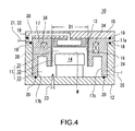
- Fig. 4 is a sectional view schematically showing an inner structure of the thin film production apparatus 10.
- the thin film production apparatus 10 includes the vacuum tank 12, a lid body 15 closing an upper portion of the vacuum tank 12, the stage 14 for supporting the substrate W, and the gas head 13 mounted to the lid body 15 so as to be opposed to the stage 14.
- a spatial area between the gas head 13 and the stage 14 serves as a reaction space 31 in which the material gas and the reaction gas react with each other to form a metal thin film on the substrate W. Further, between the vacuum tank 12 and the lid body 15, an inner block 17 for determining a volume of the reaction space 31 is disposed.
- the inner block 17 is formed as a single ring-like block body provided between an inner wall surface of the vacuum tank 12 and an outer circumferential portion of the stage 14. Specifically, in this embodiment, the inner block 17 has an annular structure. An outer diameter of the inner block 17 is substantially the same as an inner diameter of the vacuum tank 12. An inner circumferential portion of the inner block 17 is opposed to an outer circumferential portion of the gas head 13 and the outer circumferential portion of the stage 14. An inner diameter of the inner block 17 is adjusted to an intended width of the reaction space 31 to thereby determine the volume of the reaction space 31.
- the inner block 17 plural inner blocks are prepared in order to form an optimum reaction space in accordance with a size (outer diameter of the gas head 13 and outer diameter of the stage 14) of the substrate W to be processed.
- the inner block 17 with which a width of the reaction space 31 becomes D1 is employed as shown in Fig. 4 .
- an inner block 27 with which a width of the reaction space 31 becomes D2 is employed as shown in Fig. 5 .
- the inner block 17 is different from the inner block 27 only in inner diameter, and description of the inner block 17 will thus be made as a representative example in the following description.
- the inner block 17 is made of a metal material such as aluminum and stainless steel and is disposed between the vacuum tank 12 and the lid body 15 to determine the volume of the reaction space 31, and also functions as a companion flange that is used when the lid body 15 is mounted to the vacuum tank 12.
- a circumferential edge portion 17a of the inner block 17 is sandwiched between the vacuum tank 12 and the lid body 15 via annular seal members 18 and 19.
- a lower end portion 17b of the inner block 17 is mounted to a bottom portion of the vacuum tank 12 via a seal member 20. With this structure, precipitation of material elements to the inner wall surface of the vacuum tank 12 due to circulation of a deposition gas is prevented.
- the inner block 17 is provided at the lower end portion 17b side thereof with an annular recess portion 17c for properly adjusting a volume of a exhaust space with respect to the reaction space.
- the processing chamber 11 inside the vacuum tank 12 has three spaces, i.e., the reaction space 31, an exhaust path 32, and a lower space 33, defined by the inner block 17 disposed between the vacuum tank 12 and the lid body 15.
- the reaction space 31 is defined by the gas head 13, the stage 14, and the inner circumferential portion of the inner block 17.
- the exhaust path 32 is formed as an annular space between the outer circumferential portion of the stage 14 and the inner circumferential portion of the inner block 17.
- the lower space 33 is defined between the recess portion 17c of the inner block 17 and the outer circumferential portion of the stage 14.
- the lower space 33 communicates via the exhaust path 32 with the reaction space 31 and has a volume larger than the volume of the reaction space 31.
- the lower space 33 is formed with a exhaust port 24 that is an opening that penetrates the inner block 17 and the vacuum tank 12.
- the exhaust port 24 is connected with a vacuum exhaust line 25.
- a gas introduction port 23 for introducing an inert gas for controlling a gas partial pressure into the lower space 33 is provided to the bottom portion of the vacuum tank 12.
- an adhesion prevention plate 16 for preventing adhesion of the deposition material to the vacuum tank 12 and the inner block 17 is mounted.
- the inner block 17 has a built-in heating source 34 capable of heat-adjusting the adhesion prevention plate 16 to a predetermined temperature.
- the heating source 34 is composed of a heater, but may alternatively be formed of a circulation flow path of a heating medium or the like. It should be noted that the vacuum tank 12 may be formed so as to be capable of being temperature-controlled apart from the inner block 17.
- the stage 14 is composed of a hot plate capable of heating the substrate W to a predetermined temperature.
- a mechanism for holding the substrate W may be an electrostatic chuck mechanism or a mechanical clamp mechanism.
- the substrate W is conveyed to the stage 14 and conveyed from the stage 14 to outside the vacuum tank 12 by a not-shown substrate convey robot via an opening 28 penetrating the inner block 17 and the vacuum tank 12.
- the gas head 13 is composed of a shower head for uniformly supplying the deposition gas to the surface of the substrate W.
- Introduction of the deposition gas into the gas head 13 is performed through a gas introduction line 30 structured by connecting flow paths respectively formed in the lid body 15 and the inner block 17.
- the gas introduction line 30 is connected to the reaction gas supply line 21 and/or the material gas supply line 22.
- the volume of the reaction space 31 is determined by the inner block 17 disposed inside the vacuum tank 12, whereby the volume of the reaction space is optimized by merely altering the size of the inner diameter of the inner block 17 without altering the size of the vacuum tank 12. Further, since the inner block 17 has the built-in heating source 34, the wall surface defining the reaction space 31 can be optimally temperature-controlled, use efficiency of the deposition gas supplied by the gas head 13 can be improved, and, at the same time, the deposited film quality can be improved.
- film formation on plural kinds of substrates having different sizes can be performed with a common vacuum tank, and there is no need to design and alter the vacuum tank for each substrate and for each process. Further, increase of the number of apparatus structural components to be prepared for each size of the substrate to be processed can be minimized, whereby the cost of the components can be reduced, and, while simplifying assembling operation, product inspection operation, and adjusting operation, excellent deposition efficiency and stable film formation can be realized.
- the processing chamber 11 inside the vacuum tank 12 is constituted by the reaction space 31, the exhaust path 32, and the lower space 33 having the above-mentioned structures, thereby realizing isotropic exhaust of the deposition gas supplied to the reaction space 31 and contributing to improvement of deposition efficiency.
- the volume of a secondary side of the exhaust path 32 i.e., the lower space 33
- the inert gas for controlling gas partial pressure is introduced into the lower space 33, whereby precipitation temperature of the material elements in the deposition gas with respect to the inner wall surface of the lower space 33 can be decreased.
- adhesion of the deposition material to the lower space 33 is suppressed, and the temperature of the wall surface defining the lower space 33 can be decreased, thereby decreasing energy required to heat the inner block 17, i.e., decreasing power consumption.
- the gas introduction line 30 for introducing the deposition gas into the gas head 13 is formed in the lid body 15 and the inner block 17, so an introduction mechanism for the deposition gas is not required to be provided to the vacuum tank 12.
- the introduction mechanism for the deposition gas can readily be constituted.
- the thin film production apparatus 10 by structuring the thin film production apparatus 10 such that alterations required in the thin film production apparatus 10 for each substrate size and for each process rely on the alterations of the inner block 17, the amount of alterations of the parts other than the inner block 17 in the thin film production apparatus 10 can be reduced, and stable film formation with improved deposition efficiency and with less particles becomes possible.
- FIG. 6 schematically shows a structure of a thin film production apparatus 40 according to another embodiment of the present invention. It should be noted that, in the figure, parts corresponding to those of the thin film production apparatus 10 described above are denoted by the same reference symbols and detailed description thereof will be omitted.
- the thin film production apparatus 40 includes, between the lid body 15 and the inner block 17, a spacer block 41 for adjusting a distance between the stage 14 and the gas head 13.
- the spacer block 41 is mounted to the lid body 15 via a seal member 42 and to the inner block 17 via a seal member 43.
- a gas introduction line 44 for introducing the deposition gas into the gas head 13 is structured by connecting flow paths respectively formed in the lid body 15, the spacer block 41, and the inner block 17.
- the thin film formation apparatus 40 of this embodiment not only by adjusting the inner diameter of the inner block 17 but also by adjusting the distance between the stage 14 and the gas head 13 with the spacer block 41, a height and the volume of the reaction space 31 can be optimized for each substrate size and for each kind of process. It should be noted that, instead of additionally providing the spacer block 41, the inner block 17 may have the function of the space block 41.
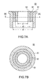
- an inner block 50 may, for example, be structured as a combined body of three annular block bodies 51, 52, and 53 having inner diameters d1, d2, and d3, respectively, and the inner side block bodies 52 and 53 may be attached/detached depending on the substrate size. It should be noted that the number of the annular block bodies to be combined is not limited to the example shown in the figure.
Landscapes
- Chemical & Material Sciences (AREA)
- General Chemical & Material Sciences (AREA)
- Chemical Kinetics & Catalysis (AREA)
- Engineering & Computer Science (AREA)
- Materials Engineering (AREA)
- Mechanical Engineering (AREA)
- Metallurgy (AREA)
- Organic Chemistry (AREA)
- Chemical Vapour Deposition (AREA)
- Electrodes Of Semiconductors (AREA)
- Physical Vapour Deposition (AREA)
Abstract
Description
- The present invention relates to a thin film production apparatus such as an MOCVD apparatus. More specifically, the present invention relates to a thin film production apparatus and an inner block for a thin film production apparatus capable of adjusting a volume of a reaction space depending on a size of a substrate to be processed.
- In recent years, in the field of semiconductors, manufacturers of semiconductor production apparatuses tend to provide apparatuses diversified in order to meet various process demands, but are, at the same time, required to meet demands for improvement of deposition efficiency, earlier delivery, and cost reduction.
- Meanwhile, in the past, thin film production apparatuses for producing a thin film by employing an MOCVD (Metal Organic Chemical Vapor Deposition) method have been known (refer to
Patent Document 1 below). With regard to the semiconductor production apparatuses employing this kind of chemical reaction process, there is a strong demand in the market to improve deposition efficiency, i.e., gas use efficiency. Specifically, a long-term apparatus operation cost is more emphasized recently than a price of a semiconductor production apparatus itself because most liquid materials are expensive, so the deposition efficiency can be a decisive factor in selection of an apparatus. - Patent Document 1: Japanese Patent Application Laid-open No.
2004-35971 - However, one semiconductor production apparatus is constituted by a plurality of process modules, and one process module is constituted by, for example, approximately a thousand components. Diversification of apparatuses causes differences in structural components, which then requires as many assembly operation processes and component adjusting methods as the number of the different components, with the result that operation categories are increased in number to inhibit the assembly operations and product inspection operations, whereby the early delivery demand cannot be met. Further, the increased number of component categories also increases the number of order operations, delivery date confirmation operations, and reception operations as much as the number of the components, thereby bulging purchase-related operations. Moreover, from a viewpoint of purchasing the components, the increased number of component categories may inhibit budget priority of bulk purchase, and, in addition, delivery of each component may lead to a failure in meeting the early delivery demand. In addition, from a viewpoint of selling the components, the different components require different settings of processing machines and cutting tools, whereby labor hours required for changing the setting backfire on prices and delivery dates.
- Meanwhile, in the thin film production apparatus employing the chemical reaction process such as the MOCVD method, in order to improve the deposition efficiency, the reaction space is required to be structured as small as possible in accordance with the substrate. However, in the case where the vacuum tank size is altered for each substrate size, various components such as piping and equipment connected to the vacuum tank are changed. The alteration of the mechanical components may lead to alteration of electronic components such as sensors and wirings, and the alteration of the electronic components may alter control software, which eventually leads to a large number of component categories. Further, in the entire field of semiconductors, there is a large demand for decreasing CO2 (carbon dioxide), so there is a strong demand in decreasing operation power consumption also from viewpoints of apparatus operation cost reduction and CO2 reduction.
- The present invention has been made in view of the above-mentioned problems, and it is an object of the present invention to provide a thin film production apparatus and an inner block for a thin film production apparatus that enable cost reduction and improvement of deposition efficiency by employing a common component. Means for solving the Problems
- To solve the above-mentioned problems, according to the present invention, a thin film production apparatus having a vacuum tank, a lid body closing an upper portion of the vacuum tank, a stage for supporting a substrate to be processed, and a gas head mounted to the lid body such that the gas head is opposed to the stage, includes an inner block disposed between the vacuum tank and the lid body and including a built-in heating source, for determining a volume of a reaction space between the stage and the gas head.
- According to the present invention, by determining a volume of the reaction space by the inner block disposed inside the vacuum tank, the volume of the reaction space is optimized by merely altering a size of the inner block without altering a size of the vacuum tank. With this structure, film formation on plural kinds of substrates having different sizes is enabled using the common vacuum tank. Further, increase of the number of apparatus structural components to be prepared for each size of the substrate to be processed can be minimized, whereby the cost of the components can be reduced, and, while simplifying assembling operation, product inspection operation, and adjusting operation, excellent deposition efficiency and stable film formation can be realized.
- Preferably, the inner block is an annular block body disposed between an inner wall surface of the vacuum tank and an outer circumferential portion of the stage, and is mounted to the vacuum tank and the lid body via seal members. With the inner block having the above structure, the volume of the reaction space can be readily optimized by merely altering an inner diameter of the block body in accordance with the substrate size.
- Further, the inner block includes a heating source, and heat adjustment is executed to a predetermined process temperature during film formation, thereby improving gas use efficiency and deposition efficiency. Moreover, by merely maintaining the predetermined process temperature at least only in an area of the inner block opposed to the reaction space instead of the entire inner block, power consumption can be decreased. In this case, by forming the spatial area opposed to a low temperature portion of the inner block larger in volume than the reaction space, and preferably by introducing an inert gas for controlling gas partial pressure into the spatial area, precipitation of material elements of the deposition gas onto a surface of the low temperature portion of the inner block can be suppressed.
- As described above, according to the present invention, film formation on plural kinds of substrates having different sizes is enabled using a common vacuum tank. Further, increase of the number of apparatus structural components to be prepared for each size of the substrate to be processed can be minimized, whereby the cost of the components can be reduced, and, while simplifying assembling operation, product inspection operation, and adjusting operation, excellent deposition efficiency and stable film formation can be realized.
-
- [
Fig. 1 ] A piping arrangement diagram of a thin film production apparatus according to an embodiment of the present invention. - [
Fig. 2 ] A diagram showing an example of a configuration of a reaction gas source. - [
Fig. 3 ] A diagram showing another example of the configuration of the reaction gas source. - [
Fig. 4 ] A schematic sectional diagram showing a structure of the thin film production apparatus according to the embodiment of the present invention. - [
Fig. 5 ] A schematic sectional diagram showing another structure of the thin film production apparatus according to the embodiment of the present invention. - [
Fig. 6 ] A schematic sectional diagram showing a structure of a thin film production apparatus according to another embodiment of the present invention. - [
Figs. 7 ] Diagrams showing a modification example of a structure of an inner block for the thin film production apparatuses according to the embodiments of the present invention,Fig. 7A being a side sectional view thereof,Fig. 7B being a sectional view thereof taken along the line [B]-[B] ofFig. 7A . -
- 10, 40
- thin film production apparatus
- 11
- processing chamber
- 12
- vacuum tank
- 13
- gas head
- 14
- stage
- 15
- lid body
- 16
- adhesion prevention plate
- 17, 27, 50
- inner block
- 18, 19, 20, 42, 43
- seal member
- 21
- reaction gas supply line
- 22
- material gas supply line
- 23
- gas introduction port for controlling partial pressure
- 24
- exhaust port
- 25
- vacuum exhaust line
- 26
- vacuum exhaust apparatus
- 30, 44
- gas introduction line
- 31
- reaction space
- 32
- exhaust path
- 33
- lower space
- 34
- heating source
- 41
- spacer block
- W
- substrate
- Hereinafter, embodiments of the present invention will be described with reference to the drawings.
-
Fig. 1 is a piping arrangement diagram of a deposition gas supply line and a vacuum exhaust line of a thinfilm production apparatus 10 according to an embodiment of the present invention. It should be noted that, in the description, the "deposition gas" refers to an unmixed gas such as a material gas, a reaction gas, or an inert gas or a mixed gas thereof used in a chemical reaction. - The thin
film production apparatus 10 according to this embodiment includes avacuum tank 12 having a processing chamber (film formation chamber) 11 formed therein, agas head 13 for introducing a deposition gas into theprocessing chamber 11, and astage 14 disposed in theprocessing chamber 11, for supporting a substrate to be processed (hereinafter referred to as "substrate") W such as a semiconductor wafer or a glass substrate. - The
processing chamber 11 is connected via avacuum exhaust line 25 to avacuum exhaust apparatus 26, and is structured such that, when opening a main valve V0, theprocessing chamber 11 can be evacuated to a predetermined reduced-pressure atmosphere. Thestage 14 is arranged so as to be opposed to thegas head 13. Thestage 14 is made of, for example, a hot plate, and is capable of heating the substrate W placed on thestage 14 to a predetermined temperature. - The
gas head 13 is connected to a reactiongas supply line 21 communicating with a reaction gas source and a materialgas supply line 22 communicating with a material gas source as will be described later in detail, and introduces a reaction gas and a material gas, or a mixed gas thereof into theprocessing chamber 11. In this embodiment, thegas head 13 employs a shower head provided with plural gas ejection holes. - As the reaction gas, NH3 (ammonia gas), H2 (hydrogen gas), or the like is used. As the material gas, an organic metal material including metallic species (Ta, Cu, Al, Ti, Zr, V, Nb) to be deposited is used, which is selected depending on an intended application (wiring film, barrier film, etc.). In this case, as the reaction gas, an activated nitride gas, e.g., ammonia gas is used so that a nitride film of the above metal is formed. As the inert gas, N2 or Ar is used.
- Herein, a description will be made of the reaction gas source. The reaction gas source is a generally-used gas source (reaction gas source, inert gas source, etc.) whose gas flow rate can be controlled using a mass flow controller (MFC) as shown in
Fig. 2 . One integration-type gas source can supply a plurality of gases therefrom.Fig. 3 exemplifies the integration-type gas source. In the example shown in the figure, areaction gas 1 is NH3, areaction gas 2 is H2, and an inert gas is N2. Unmixed gases thereof or a mixed gas thereof can be used as a gas source. - Regarding the material gas source, there is employed a system in which a solid or liquid organic metal material is gasified to obtain a material gas. In the case of the liquid material, there is employed a vaporizing system in which a liquid is supplied to a vaporizer to be vaporized, or a bubbling system. In the case of the solid material, there is employed a combined system of a material heating system in which a solid is heated to be liquefied and then vaporized by the vaporizer and the vaporizing system, a combined system of a heating system and the bubbling system, a sublimation system in which a solid material is gasified, or the like. It should be noted that the material gas is not limited to the organic metal material and can employ a gas such as WF6 generally used in a semiconductor production process.
- The reaction gas and the material gas introduced into the
processing chamber 11 chemically-react with each other_to form a metal thin film on the substrate W. A by-product and a redundant gas are discharged via thevacuum exhaust line 25. - The reaction gas and the material gas may be introduced into the
film formation chamber 11 simultaneously or separately. By opening/closing a first valve V1, the materialgas supply line 22 is switched between introduction/non-introduction of_the material gas. It should be noted that, when the first valve V1 is closed, by opening a second valve V2, the material gas can be discharged via a bypass piping 24, not via theprocessing chamber 11. In this case, the second valve V2 is closed during film formation and is opened when the film formation is finished. By supplying the material gas as described above, the material gas can be stably introduced into theprocessing chamber 11. - Further, it is possible to activate the reaction gas and then introduce the gas into the
processing chamber 11. In this embodiment, in the vicinity of thegas head 13, aradical source 29 for exciting the reaction gas supplied via the reactiongas supply line 21 to produce a radical gas is disposed. As theradical source 29, a catalytic wire heated to a high temperature, for example, is employed. -
Fig. 4 is a sectional view schematically showing an inner structure of the thinfilm production apparatus 10. The thinfilm production apparatus 10 includes thevacuum tank 12, alid body 15 closing an upper portion of thevacuum tank 12, thestage 14 for supporting the substrate W, and thegas head 13 mounted to thelid body 15 so as to be opposed to thestage 14. - A spatial area between the
gas head 13 and thestage 14 serves as areaction space 31 in which the material gas and the reaction gas react with each other to form a metal thin film on the substrate W. Further, between thevacuum tank 12 and thelid body 15, aninner block 17 for determining a volume of thereaction space 31 is disposed. - The
inner block 17 is formed as a single ring-like block body provided between an inner wall surface of thevacuum tank 12 and an outer circumferential portion of thestage 14. Specifically, in this embodiment, theinner block 17 has an annular structure. An outer diameter of theinner block 17 is substantially the same as an inner diameter of thevacuum tank 12. An inner circumferential portion of theinner block 17 is opposed to an outer circumferential portion of thegas head 13 and the outer circumferential portion of thestage 14. An inner diameter of theinner block 17 is adjusted to an intended width of thereaction space 31 to thereby determine the volume of thereaction space 31. - Herein, as the
inner block 17, plural inner blocks are prepared in order to form an optimum reaction space in accordance with a size (outer diameter of thegas head 13 and outer diameter of the stage 14) of the substrate W to be processed. In a case where the size of the substrate is, for example, Φ 200 mm, theinner block 17 with which a width of thereaction space 31 becomes D1 is employed as shown inFig. 4 . In a case where the size of the substrate is, for example, Φ 300 mm, aninner block 27 with which a width of thereaction space 31 becomes D2 is employed as shown inFig. 5 . Theinner block 17 is different from theinner block 27 only in inner diameter, and description of theinner block 17 will thus be made as a representative example in the following description. - The
inner block 17 is made of a metal material such as aluminum and stainless steel and is disposed between thevacuum tank 12 and thelid body 15 to determine the volume of thereaction space 31, and also functions as a companion flange that is used when thelid body 15 is mounted to thevacuum tank 12. Acircumferential edge portion 17a of theinner block 17 is sandwiched between thevacuum tank 12 and thelid body 15 viaannular seal members lower end portion 17b of theinner block 17 is mounted to a bottom portion of thevacuum tank 12 via aseal member 20. With this structure, precipitation of material elements to the inner wall surface of thevacuum tank 12 due to circulation of a deposition gas is prevented. Further, theinner block 17 is provided at thelower end portion 17b side thereof with anannular recess portion 17c for properly adjusting a volume of a exhaust space with respect to the reaction space. - The
processing chamber 11 inside thevacuum tank 12 has three spaces, i.e., thereaction space 31, anexhaust path 32, and alower space 33, defined by theinner block 17 disposed between thevacuum tank 12 and thelid body 15. Thereaction space 31 is defined by thegas head 13, thestage 14, and the inner circumferential portion of theinner block 17. Theexhaust path 32 is formed as an annular space between the outer circumferential portion of thestage 14 and the inner circumferential portion of theinner block 17. - The
lower space 33 is defined between therecess portion 17c of theinner block 17 and the outer circumferential portion of thestage 14. Thelower space 33 communicates via theexhaust path 32 with thereaction space 31 and has a volume larger than the volume of thereaction space 31. Further, thelower space 33 is formed with aexhaust port 24 that is an opening that penetrates theinner block 17 and thevacuum tank 12. Theexhaust port 24 is connected with avacuum exhaust line 25. Further, agas introduction port 23 for introducing an inert gas for controlling a gas partial pressure into thelower space 33 is provided to the bottom portion of thevacuum tank 12. - To the inner circumferential portion of the
inner block 17, anadhesion prevention plate 16 for preventing adhesion of the deposition material to thevacuum tank 12 and theinner block 17 is mounted. Further, theinner block 17 has a built-inheating source 34 capable of heat-adjusting theadhesion prevention plate 16 to a predetermined temperature. Theheating source 34 is composed of a heater, but may alternatively be formed of a circulation flow path of a heating medium or the like. It should be noted that thevacuum tank 12 may be formed so as to be capable of being temperature-controlled apart from theinner block 17. - Meanwhile, the
stage 14 is composed of a hot plate capable of heating the substrate W to a predetermined temperature. A mechanism for holding the substrate W may be an electrostatic chuck mechanism or a mechanical clamp mechanism. The substrate W is conveyed to thestage 14 and conveyed from thestage 14 to outside thevacuum tank 12 by a not-shown substrate convey robot via anopening 28 penetrating theinner block 17 and thevacuum tank 12. - Further, the
gas head 13 is composed of a shower head for uniformly supplying the deposition gas to the surface of the substrate W. Introduction of the deposition gas into thegas head 13 is performed through agas introduction line 30 structured by connecting flow paths respectively formed in thelid body 15 and theinner block 17. Thegas introduction line 30 is connected to the reactiongas supply line 21 and/or the materialgas supply line 22. - In the thin
film production apparatus 10 according to this embodiment structured as described above, the volume of thereaction space 31 is determined by theinner block 17 disposed inside thevacuum tank 12, whereby the volume of the reaction space is optimized by merely altering the size of the inner diameter of theinner block 17 without altering the size of thevacuum tank 12. Further, since theinner block 17 has the built-inheating source 34, the wall surface defining thereaction space 31 can be optimally temperature-controlled, use efficiency of the deposition gas supplied by thegas head 13 can be improved, and, at the same time, the deposited film quality can be improved. - Thus, according to this embodiment, film formation on plural kinds of substrates having different sizes can be performed with a common vacuum tank, and there is no need to design and alter the vacuum tank for each substrate and for each process. Further, increase of the number of apparatus structural components to be prepared for each size of the substrate to be processed can be minimized, whereby the cost of the components can be reduced, and, while simplifying assembling operation, product inspection operation, and adjusting operation, excellent deposition efficiency and stable film formation can be realized.
- Further, the
processing chamber 11 inside thevacuum tank 12 is constituted by thereaction space 31, theexhaust path 32, and thelower space 33 having the above-mentioned structures, thereby realizing isotropic exhaust of the deposition gas supplied to thereaction space 31 and contributing to improvement of deposition efficiency. - Specifically, the volume of a secondary side of the
exhaust path 32, i.e., thelower space 33, is made to be larger than the volume of thereaction space 31, and the inert gas for controlling gas partial pressure is introduced into thelower space 33, whereby precipitation temperature of the material elements in the deposition gas with respect to the inner wall surface of thelower space 33 can be decreased. As a result, adhesion of the deposition material to thelower space 33 is suppressed, and the temperature of the wall surface defining thelower space 33 can be decreased, thereby decreasing energy required to heat theinner block 17, i.e., decreasing power consumption. - Further, the
gas introduction line 30 for introducing the deposition gas into thegas head 13 is formed in thelid body 15 and theinner block 17, so an introduction mechanism for the deposition gas is not required to be provided to thevacuum tank 12. By merely altering theinner block 17 and the lid body 15 (gas head 13) in accordance with the substrate size, the introduction mechanism for the deposition gas can readily be constituted. - As described above, according to this embodiment, by structuring the thin
film production apparatus 10 such that alterations required in the thinfilm production apparatus 10 for each substrate size and for each process rely on the alterations of theinner block 17, the amount of alterations of the parts other than theinner block 17 in the thinfilm production apparatus 10 can be reduced, and stable film formation with improved deposition efficiency and with less particles becomes possible. - Subsequently,
Fig. 6 schematically shows a structure of a thinfilm production apparatus 40 according to another embodiment of the present invention. It should be noted that, in the figure, parts corresponding to those of the thinfilm production apparatus 10 described above are denoted by the same reference symbols and detailed description thereof will be omitted. - The thin
film production apparatus 40 according to this embodiment includes, between thelid body 15 and theinner block 17, aspacer block 41 for adjusting a distance between thestage 14 and thegas head 13. Thespacer block 41 is mounted to thelid body 15 via aseal member 42 and to theinner block 17 via aseal member 43. Further, agas introduction line 44 for introducing the deposition gas into thegas head 13 is structured by connecting flow paths respectively formed in thelid body 15, thespacer block 41, and theinner block 17. - According to the thin
film formation apparatus 40 of this embodiment, not only by adjusting the inner diameter of theinner block 17 but also by adjusting the distance between thestage 14 and thegas head 13 with thespacer block 41, a height and the volume of thereaction space 31 can be optimized for each substrate size and for each kind of process. It should be noted that, instead of additionally providing thespacer block 41, theinner block 17 may have the function of thespace block 41. - The embodiments of the present invention have been described above. As a matter of course, the present invention is not limited thereto, and various modifications can be made based on the technical ideas of the present invention.
- For example, in the above embodiments, there has been described the case where the
inner blocks Figs. 7A and 7B , aninner block 50 may, for example, be structured as a combined body of threeannular block bodies side block bodies
Claims (8)
- A thin film production apparatus including a vacuum tank, a lid body closing an upper portion of the vacuum tank, a stage for supporting a substrate to be processed, and a gas head mounted to the lid body such that the gas head is opposed to the stage, characterized by comprising
an inner block disposed between the vacuum tank and the lid body and including a built-in heating source, for determining a volume of a reaction space between the stage and the gas head. - The thin film production apparatus according to claim 1, characterized in that the inner block is an annular block body disposed between an inner wall surface of the vacuum tank and an outer circumferential portion of the stage, and is mounted to the vacuum tank and the lid body via seal members.
- The thin film production apparatus according to claim 1, characterized in that the inner block is mounted with an adhesion prevention plate on an inner circumferential portion.
- The thin film production apparatus according to claim 1, characterized in that the vacuum tank has a lower space including an exhaust port formed therein, the lower space communicating with the reaction space via an exhaust path formed between an inner circumferential portion of the inner block and the outer circumferential portion of the stage, and in that the lower space has a volume larger than a volume of_ the reaction space.
- The thin film production apparatus according to claim 4, characterized in that the lower space is provided with a gas introduction port for controlling a gas partial pressure.
- The thin film production apparatus according to claim 1, characterized in that the lid body and the inner block are formed with a gas introduction line for introducing a deposition gas into the gas head.
- The thin film production apparatus according to claim 1, characterized in that, between the lid body and the inner block, a spacer block for adjusting a distance between the gas head and the stage is disposed.
- An inner block for a thin film production apparatus including a vacuum tank, a lid body closing an upper portion of the vacuum tank, a stage for supporting a substrate to be processed, and a gas head mounted to the lid body such that the gas head is opposed to the stage, characterized in that
the inner block is composed of_an annular block body having an outer circumferential portion opposed to an inner wall surface of the vacuum tank and an inner circumferential portion opposed to an outer circumferential portion of the stage, and
the inner block is disposed between the vacuum tank and the lid body to thereby determine a volume of a reaction space between the stage and the gas head.
Applications Claiming Priority (2)
| Application Number | Priority Date | Filing Date | Title |
|---|---|---|---|
| JP2006129761 | 2006-05-09 | ||
| PCT/JP2007/059229 WO2007129622A1 (en) | 2006-05-09 | 2007-04-27 | Thin film production equipment and inner block for thin film production equipment |
Publications (2)
| Publication Number | Publication Date |
|---|---|
| EP2022872A1 true EP2022872A1 (en) | 2009-02-11 |
| EP2022872A4 EP2022872A4 (en) | 2010-07-28 |
Family
ID=38667731
Family Applications (1)
| Application Number | Title | Priority Date | Filing Date |
|---|---|---|---|
| EP07742664A Withdrawn EP2022872A4 (en) | 2006-05-09 | 2007-04-27 | THIN FILM PRODUCTION EQUIPMENT AND INTERIOR BLOCK CORRESPONDING |
Country Status (7)
| Country | Link |
|---|---|
| US (1) | US8747555B2 (en) |
| EP (1) | EP2022872A4 (en) |
| JP (1) | JP5337482B2 (en) |
| KR (1) | KR101055330B1 (en) |
| CN (1) | CN101466866B (en) |
| TW (1) | TWI365232B (en) |
| WO (1) | WO2007129622A1 (en) |
Families Citing this family (6)
| Publication number | Priority date | Publication date | Assignee | Title |
|---|---|---|---|---|
| US7824519B2 (en) * | 2007-05-18 | 2010-11-02 | Lam Research Corporation | Variable volume plasma processing chamber and associated methods |
| JP2011021264A (en) * | 2009-07-17 | 2011-02-03 | Ulvac Japan Ltd | Film deposition system |
| JP5031910B2 (en) * | 2010-06-23 | 2012-09-26 | シャープ株式会社 | Vapor growth equipment |
| CN105200396A (en) * | 2014-06-18 | 2015-12-30 | 中微半导体设备(上海)有限公司 | Metalorganic chemical vapor deposition (MOCVD) equipment and method for removing parasitic particles thereof |
| CN110042368B (en) * | 2019-05-14 | 2025-05-09 | 本源量子计算科技(合肥)股份有限公司 | A device for producing graphene heterojunction by chemical vapor deposition |
| US11881385B2 (en) * | 2020-04-24 | 2024-01-23 | Applied Materials, Inc. | Methods and apparatus for reducing defects in preclean chambers |
Family Cites Families (32)
| Publication number | Priority date | Publication date | Assignee | Title |
|---|---|---|---|---|
| US2834353A (en) | 1954-07-06 | 1958-05-13 | Albert A Rembold | Marginally punched and notched sorting cards |
| US4226208A (en) * | 1977-08-04 | 1980-10-07 | Canon Kabushiki Kaisha | Vapor deposition apparatus |
| US4524719A (en) * | 1983-09-06 | 1985-06-25 | Anicon, Inc. | Substrate loading means for a chemical vapor deposition apparatus |
| US5134965A (en) * | 1989-06-16 | 1992-08-04 | Hitachi, Ltd. | Processing apparatus and method for plasma processing |
| GB9411911D0 (en) * | 1994-06-14 | 1994-08-03 | Swan Thomas & Co Ltd | Improvements in or relating to chemical vapour deposition |
| JP3257328B2 (en) * | 1995-03-16 | 2002-02-18 | 株式会社日立製作所 | Plasma processing apparatus and plasma processing method |
| US6092486A (en) * | 1996-05-27 | 2000-07-25 | Sumimoto Metal Indsutries, Ltd. | Plasma processing apparatus and plasma processing method |
| JP3050124B2 (en) * | 1996-05-27 | 2000-06-12 | 住友金属工業株式会社 | Plasma processing equipment |
| EP0946782A1 (en) * | 1996-11-27 | 1999-10-06 | Emcore Corporation | Chemical vapor deposition apparatus |
| US5904800A (en) * | 1997-02-03 | 1999-05-18 | Motorola, Inc. | Semiconductor wafer processing chamber for reducing particles deposited onto the semiconductor wafer |
| US6258170B1 (en) * | 1997-09-11 | 2001-07-10 | Applied Materials, Inc. | Vaporization and deposition apparatus |
| US6106625A (en) * | 1997-12-02 | 2000-08-22 | Applied Materials, Inc. | Reactor useful for chemical vapor deposition of titanium nitride |
| US6273022B1 (en) * | 1998-03-14 | 2001-08-14 | Applied Materials, Inc. | Distributed inductively-coupled plasma source |
| US6129808A (en) * | 1998-03-31 | 2000-10-10 | Lam Research Corporation | Low contamination high density plasma etch chambers and methods for making the same |
| US6230651B1 (en) * | 1998-12-30 | 2001-05-15 | Lam Research Corporation | Gas injection system for plasma processing |
| US20020069970A1 (en) * | 2000-03-07 | 2002-06-13 | Applied Materials, Inc. | Temperature controlled semiconductor processing chamber liner |
| US6863835B1 (en) * | 2000-04-25 | 2005-03-08 | James D. Carducci | Magnetic barrier for plasma in chamber exhaust |
| US6554979B2 (en) * | 2000-06-05 | 2003-04-29 | Applied Materials, Inc. | Method and apparatus for bias deposition in a modulating electric field |
| US20020015855A1 (en) * | 2000-06-16 | 2002-02-07 | Talex Sajoto | System and method for depositing high dielectric constant materials and compatible conductive materials |
| JP3534716B2 (en) | 2001-05-28 | 2004-06-07 | 株式会社日立製作所 | Plasma processing method |
| EP1466034A1 (en) * | 2002-01-17 | 2004-10-13 | Sundew Technologies, LLC | Ald apparatus and method |
| US7160577B2 (en) | 2002-05-02 | 2007-01-09 | Micron Technology, Inc. | Methods for atomic-layer deposition of aluminum oxides in integrated circuits |
| JP2004035971A (en) | 2002-07-05 | 2004-02-05 | Ulvac Japan Ltd | Thin film manufacturing equipment |
| JP2004063661A (en) * | 2002-07-26 | 2004-02-26 | Hitachi Kokusai Electric Inc | Semiconductor manufacturing equipment |
| JP2004091849A (en) * | 2002-08-30 | 2004-03-25 | Tokyo Electron Ltd | Processing equipment |
| US7048837B2 (en) * | 2002-09-13 | 2006-05-23 | Applied Materials, Inc. | End point detection for sputtering and resputtering |
| JP2004149881A (en) | 2002-10-31 | 2004-05-27 | Applied Materials Inc | Plasma processing apparatus and method |
| TW200508413A (en) * | 2003-08-06 | 2005-03-01 | Ulvac Inc | Device and method for manufacturing thin films |
| US7682454B2 (en) * | 2003-08-07 | 2010-03-23 | Sundew Technologies, Llc | Perimeter partition-valve with protected seals and associated small size process chambers and multiple chamber systems |
| JP2005093576A (en) * | 2003-09-16 | 2005-04-07 | Sony Corp | Processing equipment |
| JP4361811B2 (en) | 2004-01-09 | 2009-11-11 | 東京エレクトロン株式会社 | Semiconductor manufacturing equipment |
| US8475625B2 (en) * | 2006-05-03 | 2013-07-02 | Applied Materials, Inc. | Apparatus for etching high aspect ratio features |
-
2007
- 2007-04-27 CN CN2007800216235A patent/CN101466866B/en active Active
- 2007-04-27 KR KR1020087027195A patent/KR101055330B1/en active Active
- 2007-04-27 WO PCT/JP2007/059229 patent/WO2007129622A1/en not_active Ceased
- 2007-04-27 EP EP07742664A patent/EP2022872A4/en not_active Withdrawn
- 2007-04-27 US US12/299,936 patent/US8747555B2/en active Active
- 2007-04-27 JP JP2008514456A patent/JP5337482B2/en active Active
- 2007-05-07 TW TW096116062A patent/TWI365232B/en active
Also Published As
| Publication number | Publication date |
|---|---|
| US8747555B2 (en) | 2014-06-10 |
| TWI365232B (en) | 2012-06-01 |
| JP5337482B2 (en) | 2013-11-06 |
| CN101466866A (en) | 2009-06-24 |
| TW200745374A (en) | 2007-12-16 |
| JPWO2007129622A1 (en) | 2009-09-17 |
| WO2007129622A1 (en) | 2007-11-15 |
| US20090159006A1 (en) | 2009-06-25 |
| KR101055330B1 (en) | 2011-08-08 |
| EP2022872A4 (en) | 2010-07-28 |
| KR20090018898A (en) | 2009-02-24 |
| CN101466866B (en) | 2012-10-03 |
Similar Documents
| Publication | Publication Date | Title |
|---|---|---|
| US8747555B2 (en) | Thin film production apparatus and inner block for thin film production apparatus | |
| JP5566100B2 (en) | Method and apparatus for suppressing particle contamination in a film forming system | |
| US12509768B2 (en) | Method of manufacturing semiconductor device, substrate processing apparatus and evaporation system | |
| US11286566B2 (en) | Apparatus for deposition of a III-V semiconductor layer | |
| JP4696561B2 (en) | Vaporizer and processing device | |
| KR101346598B1 (en) | Substrate processing apparatus and method for supplying solid material | |
| US7579276B2 (en) | Substrate processing apparatus and method of manufacturing semiconductor device | |
| TWI385274B (en) | Vapor phase growth device and vapor phase growth method | |
| KR101246491B1 (en) | Apparatus of manufacturing thin film and method for manufacturing thin film | |
| US20090277386A1 (en) | Catalytic chemical vapor deposition apparatus | |
| KR101015985B1 (en) | Substrate processing apparatus | |
| TWI391519B (en) | Vapor phase deposition device and vapor phase deposition method | |
| CN106148916A (en) | High temperature substrate base module and its components | |
| US20080210168A1 (en) | Single chamber, multiple tube high efficiency vertical furnace system | |
| KR20050016157A (en) | Shower head, apparatus of manufacturing thin film and method for manufacturing thin film | |
| US20240420969A1 (en) | Valve manifold for semiconductor processing | |
| US20130220222A1 (en) | Gas Distribution Apparatus with Heat Exchanging Channels | |
| US20060169201A1 (en) | Apparatus for supplying gas and apparatus for forming a layer having the same | |
| JP5135710B2 (en) | Film forming method and film forming apparatus | |
| JPWO2012026241A1 (en) | Semiconductor device manufacturing method and substrate processing apparatus | |
| US20090250006A1 (en) | Raw material feeding device and film formation system | |
| CN102051601B (en) | Thin film deposition method | |
| WO2003071003A1 (en) | Gas shower head, film forming device, and film forming method | |
| KR20140018148A (en) | Method and apparatus of forming compound semiconductor film | |
| JP4404674B2 (en) | Thin film manufacturing equipment |
Legal Events
| Date | Code | Title | Description |
|---|---|---|---|
| PUAI | Public reference made under article 153(3) epc to a published international application that has entered the european phase |
Free format text: ORIGINAL CODE: 0009012 |
|
| 17P | Request for examination filed |
Effective date: 20081125 |
|
| AK | Designated contracting states |
Kind code of ref document: A1 Designated state(s): AT BE BG CH CY CZ DE DK EE ES FI FR GB GR HU IE IS IT LI LT LU LV MC MT NL PL PT RO SE SI SK TR |
|
| AX | Request for extension of the european patent |
Extension state: AL BA HR MK RS |
|
| DAX | Request for extension of the european patent (deleted) | ||
| RBV | Designated contracting states (corrected) |
Designated state(s): DE |
|
| A4 | Supplementary search report drawn up and despatched |
Effective date: 20100628 |
|
| RIC1 | Information provided on ipc code assigned before grant |
Ipc: C23C 16/52 20060101ALI20100622BHEP Ipc: C23C 16/458 20060101ALI20100622BHEP Ipc: H01L 21/285 20060101ALI20100622BHEP Ipc: C23C 16/44 20060101AFI20080211BHEP |
|
| 17Q | First examination report despatched |
Effective date: 20130402 |
|
| STAA | Information on the status of an ep patent application or granted ep patent |
Free format text: STATUS: THE APPLICATION IS DEEMED TO BE WITHDRAWN |
|
| 18D | Application deemed to be withdrawn |
Effective date: 20130813 |