EP2022137B1 - Antennenanordnung sowie deren verwendung - Google Patents
Antennenanordnung sowie deren verwendung Download PDFInfo
- Publication number
- EP2022137B1 EP2022137B1 EP07725598.2A EP07725598A EP2022137B1 EP 2022137 B1 EP2022137 B1 EP 2022137B1 EP 07725598 A EP07725598 A EP 07725598A EP 2022137 B1 EP2022137 B1 EP 2022137B1
- Authority
- EP
- European Patent Office
- Prior art keywords
- electrically conductive
- conductive layer
- antenna
- antenna structure
- configuration according
- Prior art date
- Legal status (The legal status is an assumption and is not a legal conclusion. Google has not performed a legal analysis and makes no representation as to the accuracy of the status listed.)
- Not-in-force
Links
Images



Classifications
-
- H—ELECTRICITY
- H01—ELECTRIC ELEMENTS
- H01Q—ANTENNAS, i.e. RADIO AERIALS
- H01Q1/00—Details of, or arrangements associated with, antennas
- H01Q1/12—Supports; Mounting means
- H01Q1/22—Supports; Mounting means by structural association with other equipment or articles
- H01Q1/2208—Supports; Mounting means by structural association with other equipment or articles associated with components used in interrogation type services, i.e. in systems for information exchange between an interrogator/reader and a tag/transponder, e.g. in Radio Frequency Identification [RFID] systems
- H01Q1/2225—Supports; Mounting means by structural association with other equipment or articles associated with components used in interrogation type services, i.e. in systems for information exchange between an interrogator/reader and a tag/transponder, e.g. in Radio Frequency Identification [RFID] systems used in active tags, i.e. provided with its own power source or in passive tags, i.e. deriving power from RF signal
-
- H—ELECTRICITY
- H01—ELECTRIC ELEMENTS
- H01Q—ANTENNAS, i.e. RADIO AERIALS
- H01Q7/00—Loop antennas with a substantially uniform current distribution around the loop and having a directional radiation pattern in a plane perpendicular to the plane of the loop
-
- G—PHYSICS
- G06—COMPUTING OR CALCULATING; COUNTING
- G06K—GRAPHICAL DATA READING; PRESENTATION OF DATA; RECORD CARRIERS; HANDLING RECORD CARRIERS
- G06K19/00—Record carriers for use with machines and with at least a part designed to carry digital markings
- G06K19/06—Record carriers for use with machines and with at least a part designed to carry digital markings characterised by the kind of the digital marking, e.g. shape, nature, code
- G06K19/067—Record carriers with conductive marks, printed circuits or semiconductor circuit elements, e.g. credit or identity cards also with resonating or responding marks without active components
- G06K19/07—Record carriers with conductive marks, printed circuits or semiconductor circuit elements, e.g. credit or identity cards also with resonating or responding marks without active components with integrated circuit chips
- G06K19/077—Constructional details, e.g. mounting of circuits in the carrier
-
- G—PHYSICS
- G06—COMPUTING OR CALCULATING; COUNTING
- G06K—GRAPHICAL DATA READING; PRESENTATION OF DATA; RECORD CARRIERS; HANDLING RECORD CARRIERS
- G06K19/00—Record carriers for use with machines and with at least a part designed to carry digital markings
- G06K19/06—Record carriers for use with machines and with at least a part designed to carry digital markings characterised by the kind of the digital marking, e.g. shape, nature, code
- G06K19/067—Record carriers with conductive marks, printed circuits or semiconductor circuit elements, e.g. credit or identity cards also with resonating or responding marks without active components
- G06K19/07—Record carriers with conductive marks, printed circuits or semiconductor circuit elements, e.g. credit or identity cards also with resonating or responding marks without active components with integrated circuit chips
- G06K19/077—Constructional details, e.g. mounting of circuits in the carrier
- G06K19/07749—Constructional details, e.g. mounting of circuits in the carrier the record carrier being capable of non-contact communication, e.g. constructional details of the antenna of a non-contact smart card
-
- G—PHYSICS
- G06—COMPUTING OR CALCULATING; COUNTING
- G06K—GRAPHICAL DATA READING; PRESENTATION OF DATA; RECORD CARRIERS; HANDLING RECORD CARRIERS
- G06K19/00—Record carriers for use with machines and with at least a part designed to carry digital markings
- G06K19/06—Record carriers for use with machines and with at least a part designed to carry digital markings characterised by the kind of the digital marking, e.g. shape, nature, code
- G06K19/067—Record carriers with conductive marks, printed circuits or semiconductor circuit elements, e.g. credit or identity cards also with resonating or responding marks without active components
- G06K19/07—Record carriers with conductive marks, printed circuits or semiconductor circuit elements, e.g. credit or identity cards also with resonating or responding marks without active components with integrated circuit chips
- G06K19/077—Constructional details, e.g. mounting of circuits in the carrier
- G06K19/07749—Constructional details, e.g. mounting of circuits in the carrier the record carrier being capable of non-contact communication, e.g. constructional details of the antenna of a non-contact smart card
- G06K19/07773—Antenna details
- G06K19/07777—Antenna details the antenna being of the inductive type
- G06K19/07779—Antenna details the antenna being of the inductive type the inductive antenna being a coil
-
- G—PHYSICS
- G06—COMPUTING OR CALCULATING; COUNTING
- G06K—GRAPHICAL DATA READING; PRESENTATION OF DATA; RECORD CARRIERS; HANDLING RECORD CARRIERS
- G06K19/00—Record carriers for use with machines and with at least a part designed to carry digital markings
- G06K19/06—Record carriers for use with machines and with at least a part designed to carry digital markings characterised by the kind of the digital marking, e.g. shape, nature, code
- G06K19/067—Record carriers with conductive marks, printed circuits or semiconductor circuit elements, e.g. credit or identity cards also with resonating or responding marks without active components
- G06K19/07—Record carriers with conductive marks, printed circuits or semiconductor circuit elements, e.g. credit or identity cards also with resonating or responding marks without active components with integrated circuit chips
- G06K19/077—Constructional details, e.g. mounting of circuits in the carrier
- G06K19/07749—Constructional details, e.g. mounting of circuits in the carrier the record carrier being capable of non-contact communication, e.g. constructional details of the antenna of a non-contact smart card
- G06K19/07773—Antenna details
- G06K19/07777—Antenna details the antenna being of the inductive type
- G06K19/07779—Antenna details the antenna being of the inductive type the inductive antenna being a coil
- G06K19/07783—Antenna details the antenna being of the inductive type the inductive antenna being a coil the coil being planar
-
- H—ELECTRICITY
- H01—ELECTRIC ELEMENTS
- H01Q—ANTENNAS, i.e. RADIO AERIALS
- H01Q1/00—Details of, or arrangements associated with, antennas
- H01Q1/12—Supports; Mounting means
- H01Q1/22—Supports; Mounting means by structural association with other equipment or articles
-
- Y—GENERAL TAGGING OF NEW TECHNOLOGICAL DEVELOPMENTS; GENERAL TAGGING OF CROSS-SECTIONAL TECHNOLOGIES SPANNING OVER SEVERAL SECTIONS OF THE IPC; TECHNICAL SUBJECTS COVERED BY FORMER USPC CROSS-REFERENCE ART COLLECTIONS [XRACs] AND DIGESTS
- Y10—TECHNICAL SUBJECTS COVERED BY FORMER USPC
- Y10T—TECHNICAL SUBJECTS COVERED BY FORMER US CLASSIFICATION
- Y10T29/00—Metal working
- Y10T29/49—Method of mechanical manufacture
- Y10T29/49002—Electrical device making
- Y10T29/49016—Antenna or wave energy "plumbing" making
- Y10T29/49018—Antenna or wave energy "plumbing" making with other electrical component
Definitions
- the invention relates to an antenna arrangement which comprises at least one electrically insulating carrier substrate and at least one electrically conductive layer applied on at least one side of the carrier substrate.
- the invention further relates to a use of the antenna arrangement.
- Such antenna arrangements are made DE 196 29 269 A1 known for smart cards.
- the antenna structure is produced here by etching an electrically conductive layer, which is arranged on an electrically insulating plastic layer and partially printed with etching-resistant photoresist. In the areas of the electrically conductive layer which are not coated by photoresist, the latter is removed by etching, the regions of the electrically conductive layer which are covered with photoresist in the form of a conductor track or antenna structure remaining on the plastic layer. Subsequently, if necessary, the photoresist is removed and the antenna structure is covered with protective varnish.
- Such a method for producing an antenna structure is relatively time consuming. Furthermore, due to the large-area removal of the electrically conductive layer, large quantities of waste material must be disposed of or recycled.
- the DE 10 2004 040 831 A1 describes a radio-label-capable outer packaging.
- This outer packaging has at least one carrier and an electrically conductive layer.
- the electrically conductive layer has a structure which makes it possible for an electrical component to supply or retain information through the outer packaging to the outside and / or to supply it with energy through the outer packaging.
- the structure divides the electrically conductive layer into at least two surfaces.
- electrical components for example an antenna or a capacitor, may also be formed in the conductive surface.
- regions of the electrically insulating layer which do not belong to the at least one antenna structure to remain on the carrier substrate.
- the subdivision of these regions of the electrically conductive layer into island regions which are at least electrically insulated from one another does not impair the antenna performance, since the formation of eddy currents or wave reflections, which are disturbing for the use of the antenna arrangement in the electric field, is significantly reduced or even prevented ,
- antenna arrangement according to the invention is particularly inexpensive to produce and thus suitable for mass-produced articles such as labels or the like.
- the formation of the island regions does not have to be carried out on all sides of the contour of the at least one antenna structure, but that it is sufficient for electrical operation if the remaining, not belonging to at least one antenna structure parts of the electrically conductive layer in at least two of each other electrically separate areas are divided.
- antenna structures are often connected to electrical conductors that electrically connect an antenna structure with other components and, of course, can not be divided into island areas, since it depends on a good electrical conductivity of the tracks.
- each island region has a maximum dimension that is ⁇ 50% of a maximum dimension of the at least one antenna structure.
- each island region has a maximum dimension which is ⁇ 25% of the maximum dimension of the at least one antenna structure, in particular ⁇ 10% of the maximum dimension of the at least one antenna structure.
- the exact size of the island regions may be different for each intended use of an antenna structure, for example for lower frequencies greater than for larger frequencies of the electromagnetic radiation.
- the island structures must continue to be not uniform in this case. Thus, specific effects, such as a directional dependence or a frequency dependence, can be promoted by the formation of specific island structures.
- the electrically conductive layer is separated from each point of the at least one antenna structure to at least one distance A from the at least one antenna structure in island areas, wherein the distance A at least 50% of the maximum dimension of the at least one antenna structure.
- this does not apply to the interconnects already mentioned above, with which an antenna structure is optionally electrically contacted.
- an electrical isolation trench is formed between adjacent island regions in that, seen in the region of a contour of an island region perpendicular to the electrically conductive layer, the electrically conductive layer is severed or a layer thickness of the electrically conductive layer is reduced.
- an isolation trench seen perpendicular to at least one electrically conductive layer has a width of less than 1 mm.
- the width of the isolation trench is significantly smaller, in particular ⁇ 100 microns.
- isolation trench can be done in different ways.
- known methods such as stamping, etching, laser cutting, scratching, embossing, nanoimprint lithography or the like can be used.
- This preferred method provides a particularly economical, environmentally friendly and production-safe etch-assisted punching method which, in addition to a very high process speeds, has the further advantage that cost-effective, simply shaped punching tools can be used and, moreover, conductor structures can be achieved to below one millimeter. Thus, areas up to 800 ⁇ m wide can also be achieved with ductile materials (for example aluminum, copper).
- the preferred method which can be carried out in particular continuously, is feasible with conventional punching machines, standard tools and etching equipment, which can be modified inexpensively and without great technical effort.
- the punching is followed, in particular directly, by an etching process adapted to the respective electrically conductive material of the electrically conductive layer.
- a surface activation of the stamped electrically conductive layer takes place at the same time, at least in regions, after impurities or oxide layers possibly present on the surface of the electrically conductive layer due to the etching process are removed.
- a subsequent in-line process step such as a bonding method for electrically connecting the antenna structure with a chip, an adhesive bonding method in which a conductive adhesive is applied, or a soldering method. Due to the surface activation, there are significant advantages in terms of the achievable adhesion and quality of the electrical contact.
- a complete punching of the carrier substrate can be avoided in the method according to the invention, since a greater tolerance of the die gap must be maintained so that the carrier substrate still has a sufficiently high tear strength even after punching in order to be optimally processed.
- the at least one antenna structure has the form of a spiral with at least one turn, which encloses a second area area, wherein the enclosed second area area is subdivided into island areas.
- a spiral but not only spiral structures are understood that are based essentially on the circular or elliptical shape.
- Spiral shapes which have an outer circumference in the form of a rectangle, polygon or meandering shape, are here to fall under the term spiral.
- the formation of eddy currents within the spiral trapped surface areas of the electrically conductive layer is effectively prevented by the subdivision of the electrically conductive layer into island regions.
- the at least one turn is enclosed by a further, second surface area which is subdivided into island areas. This also prevents the effect of eddy current formation, which is in which the turn enclosing further second surface area is formed.
- the subdivision of the further second surface area into island areas also prevents an occurrence of eddy currents or a mutual induction and the occurrence of wave reflections.
- the at least one antenna structure is designed as a dipole, T-shaped, L-shaped, U-shaped or as a combination of such antenna structures.
- antenna structure depends heavily on the radio frequency used, on nearfield or far field use, and on the nature of the coupling.
- antenna structures for the low frequency to high frequency range typically frequencies ⁇ 50MHz, most commonly 125 to 135 kHz, 8.2 MHz or 13.56 MHz
- antenna structures for the ultra-high frequency to microwave range typically > 100 MHz, most commonly 400 to 500 MHz, 850 to 950 MHz and 2 to 2.5 GHz
- the exact form of an antenna structure depends on the respective field of application. For example, an adaptation to a transponder chip, an optimization of the range or an adjustment with regard to the highest possible direction independence takes place.
- the carrier substrate has a thickness in the range of 10 ⁇ m to 5 mm. It continues Preferably, when the carrier substrate comprises a plastic film, in particular made of PET, PP, PPS, PES, PEN or polyimide, and / or a paper or cardboard layer. In particular, it can also be provided that the carrier substrate comprises at least two different layers, such as paper and plastic film. In this case, one or more adhesive layers can be integrated.
- the carrier substrate may be formed either rigid or flexible.
- the carrier substrate may have a certain own functionality. It may be formed, for example, as a sticker or label and in this case in particular have product information, a bar code and the like.
- the carrier substrate can form a packaging material or serve as a substrate for an optical and / or electrical component.
- a quasicontinuous process is understood to be a processing of isolated carrier substrate sections which are processed in series one after the other and / or are supplied to the consecutive process steps of the method side by side without intermediate storage.
- a continuous process is understood as one in which the carrier substrate is quasi-continuous, in particular flexible and band-shaped, configured and fed without intermediate storage to the successive process steps of the process, in particular in a roll-to-roll process is processed. The carrier substrate is thereby withdrawn from a supply roll, processed, in particular by the preferred combined stamping-etching process, and then wound up on another roll.
- the at least one electrically conductive layer is applied over the full area on one side of the carrier substrate. But it is also possible to provide the electrically conductive layer only partially on one side of the carrier substrate.
- the at least one electrically insulating carrier substrate comprises at least one first electrically conductive layer applied to a first side of the carrier substrate
- the at least one electrically insulating carrier substrate has at least one second electrically conductive layer applied to a second side of the carrier substrate comprises, and when the at least one first electrically conductive layer and / or the at least one second electrically conductive layer has at least one antenna structure.
- at least one electrically conductive layer is applied to each side of the carrier substrate and may each comprise one or more antenna structures. In this case, either only one or both electrically conductive layers can be structured as described.
- the at least one electrically conductive layer has a thickness in the range of 10 nm to 100 ⁇ m.
- the electrically conductive layer is formed of metal, a metal alloy, a conductive paste, a conductive ink or a conductive organic based material.
- metal or constituents of the metal alloys copper, nickel, aluminum, chromium, iron, zinc, tin, silver, gold, platinum and cobalt have proven themselves.
- conductive pastes preferably silver or Kupferleitpasten be used. Also pastes containing a mixture of organic conductive and inorganic conductive materials have been proven.
- Conductive inks contain, for example, conductive materials such as silver in the form of a silver complex or as nanoparticles, often requiring a temperature step after the application of the ink.
- the at least one electrically conductive layer comprises at least two different electrically conductive layer layers.
- a copper layer and a gold layer disposed thereon can be used as the electrically conductive layer using the above-described combined punching and etching method which is preferred for structuring the electrically conductive layer.
- the gold layer is cut through and then the etching is carried out, wherein an etchant is chosen so that it is matched to the copper and the gold does not or only slightly attacks.
- the etchant increasingly attacks in the region of the punching gap, in which the copper for the etchant is freely accessible and activated, while a superficial removal of the electrically conductive layer due to the gold plating is largely avoided.
- the application of the at least one electrically conductive layer on the carrier substrate can be carried out in different ways, wherein different methods can be used in combination.
- methods such as lamination, sticking, sputtering, vapor deposition, casting, printing, electroplating, etc. are suitable.
- the contour of at least one island region is in the form of an alphanumeric character, a symbol, a graphic representation, a geometric figure or a figurative representation.
- At least one island structure can be used so that it forms another technical component, such as an electrode (in particular for an optical element), a sensor, a battery, a photovoltaic cell, an electrical switch or button and the like.
- the antenna arrangement may comprise not only one but a plurality of antenna structures surrounded by island structures, which are arranged on one or both sides of the carrier substrate.
- radio tags such as RFID tags (radio frequency identification tags)
- RFID tags radio frequency identification tags
- EPC Electronic Product Code
- EAS Electronic Article Surveillance
- Such radio tags are based on nationally and internationally approved frequency bands for signal transmission, typically: 125-135 kHz, 13.56 MHz, 860-950 MHz or 2.45 GHz. Sometimes, however, other frequency bands can be used, such. Eg 1 - 9 MHz for anti-theft tags. Typically, frequency ranges of 1.86 to 2.18 MHz and 7.44 to 8.73 MHz are used for this application.
- a helical antenna arrangement to form an RFID tag for the high-frequency range, in particular for a frequency of 13.56 MHz.
- Radio tags or RFID tags are often used to secure and label outer packaging of food, tobacco, etc. Furthermore, an application in the field of logistics, especially in automation on the assembly line, the package logistics and the so-called electronic product code EPC ® , as sought by the international association EPCglobal, regarding a logistics chain from the manufacturer of a product to the supermarket. Furthermore, RFID tags are used for the purpose of identification, such as for ski passes, company passes, passports and the like.
- Such "smart tags” which, in addition to an RFID function, have additional functions and for which the antenna arrangements according to the invention are likewise suitable.
- such "smart tags” are capable of recording a temperature history, providing the function of a credit card or acting as a sensor.
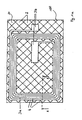
- FIG. 1a shows an antenna arrangement 100 in plan view with respect to an electrically conductive layer 20 made of copper.
- the electrically conductive layer 20 is patterned by means of stamping and subsequent etching, wherein an antenna structure 3a in the form of a spiral with electrical contact surfaces 3b is formed.
- the areas of the electrically conductive layer 20, which are arranged within the antenna structure 3a and outside of this, are also divided into electrically isolated, island-shaped island regions 2 by means of stamping and subsequent etching.
- isolation trenches 4 see also FIG. 1b
- isolation trenches 4 are arranged between the individual turns of the antenna structure 3a.
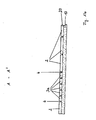
- FIG. 1b shows a portion of the antenna assembly 100 FIG. 1a in section A - A '. From this view, the carrier substrate 10, which consists of PET film of thickness 12 microns is formed, recognizable, on which the electrically conductive layer 20 has been arranged made of copper and in the form of the antenna structure 3a and the island regions 2 has been structured.
- the carrier substrate 10 which consists of PET film of thickness 12 microns is formed, recognizable, on which the electrically conductive layer 20 has been arranged made of copper and in the form of the antenna structure 3a and the island regions 2 has been structured.
- FIG. 2a shows a further antenna arrangement 100 'in plan view with respect to an electrically conductive layer 20' made of copper.
- the electrically conductive layer 20 ' is patterned by means of stamping and subsequent etching, wherein a T-shaped antenna structure 3' is formed.
- the regions of the electrically conductive layer 20 'which are arranged around the antenna structure 3' are likewise divided into electrically insulated, rectangular island regions 2 'by means of stamping and subsequent etching.
- isolation trenches 4 ' see also FIG. 2b
- Such isolation trenches 4' are arranged between the individual island regions 2 '.
- FIG. 2b shows a portion of the antenna assembly 100 ' FIG. 2a in section B - B '. From this view, the carrier substrate 10 ', which is formed from PET film of thickness 12 microns, can be seen, on which the electrically conductive layer 20' made of copper and in the form of the antenna structure 3 'and the island regions 2' has been structured ,
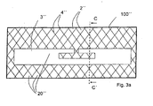
- FIG. 3a shows a further antenna arrangement 100 "in plan view with respect to an electrically conductive layer 20" made of copper.
- the electrically conductive layer 20 has been patterned by means of stamping and subsequent etching, wherein a dipole-shaped antenna structure 3" is formed.
- the portions of the electrically conductive layer 20 "disposed around the antenna structure 3" are also by means of stamping and subsequent etching in electrically isolated from each other, diamond-shaped island areas 2 "between the island areas 2" and the antenna structure 3 "are isolation trenches 4" (see also FIG. 3b ) educated. Furthermore, “such isolation trenches 4" are arranged between the individual island regions 2.
- FIG. 3b shows a portion of the antenna assembly 100 "from FIG. 3a in section C - C '.
- the carrier substrate 10 " which is formed from PET film of thickness 12 microns, can be seen, on which the electrically conductive layer 20" made of copper and in the form of the antenna structure 3 "and the island regions 2" has been structured ,
- FIG. 4 shows an application example of an antenna arrangement according to FIG. 3a in the region of a rectangularly shaped package 30.
- an RFID antenna in the form of the antenna structure 3 " is integrated, which is surrounded by not numbered island areas here and which cover the surface of the packaging.
Landscapes
- Engineering & Computer Science (AREA)
- Computer Hardware Design (AREA)
- Microelectronics & Electronic Packaging (AREA)
- Physics & Mathematics (AREA)
- General Physics & Mathematics (AREA)
- Theoretical Computer Science (AREA)
- Computer Networks & Wireless Communication (AREA)
- Details Of Aerials (AREA)
Description
- Die Erfindung betrifft eine Antennenanordnung, welche mindestens ein elektrisch isolierendes Trägersubstrat und mindestens eine, auf mindestens einer Seite des Trägersubstrats aufgebrachte elektrisch leitende Schicht umfasst. Die Erfindung betrifft weiterhin eine Verwendung der Antennenanordnung.
- Solche Antennenanordnungen sind aus
DE 196 29 269 A1 für Chipkarten bekannt. Die Antennenstruktur wird hier durch Ätzen einer elektrisch leitenden Schicht hergestellt, welche auf einer elektrisch isolierenden Kunststoffschicht angeordnet und bereichsweise mit ätzresistentem Photolack bedruckt wird. In den nicht von Photolack beschichteten Bereichen der elektrisch leitenden Schicht wird diese durch Ätzen entfernt, wobei die in Form einer Leiterbahn- bzw. Antennenstruktur mit Photolack bedeckten Bereiche der elektrisch leitenden Schicht auf der Kunststoffschicht verbleiben. Anschließend wird gegebenenfalls der Photolack entfernt und die Antennenstruktur mit Schutzlack bedeckt. - Ein derartiges Verfahren zur Herstellung einer Antennenstruktur ist relativ zeitaufwendig. Weiterhin entstehen aufgrund des großflächig notwendigen Abtrags der elektrisch leitenden Schicht große Mengen an Abfallstoffen, die entsorgt bzw. recycelt werden müssen.
- Um die Menge an durch Ätzen zu entfernendem Material und gleichzeitig den Bedarf an Ätzmittel zu vermindern wurde daher versucht, die elektrisch leitende Schicht lediglich im Bereich der Konturen der Antennenstruktur durch Ätzen zu entfernen.
- Es hat sich jedoch gezeigt, dass in den auf dem elektrisch isolierenden Trägersubstrat verbleibenden, an die Antennenstruktur angrenzenden Bereichen der elektrisch leitenden Schicht im elektrischen Betrieb der Antennenstruktur elektrische Effekte auftreten, die zu einer Beeinträchtigung der Antennenleistung führen. So werden beispielsweise in von der Antennenstruktur umschlossenen Bereichen der elektrisch leitenden Schicht störende Wirbelströme ausgebildet. Weiterhin können Bereiche der elektrisch leitenden Schicht Störungen aufgrund einer Reflexion von elektromagnetischen Wellen erzeugen.
- Die
DE 10 2004 040 831 A1 beschreibt eine funketikettfähige Umverpackung. Diese Umverpackung weist zumindest einen Träger und eine elektrisch leitfähige Schicht auf. Die elektrisch leitfähige Schicht weist hierbei eine Struktur auf, die es einem elektrischen Bauteil ermöglicht, Informationen durch die Umverpackung nach Außen zu liefern oder zu halten und/oder zur Energieversorgung durch die Umverpackung hindurch zu speisen. Die Struktur unterteilt die elektrisch leitenden Schicht hierzu in zumindest zwei Flächen. Weiter können in der leitfähigen Fläche auch elektrische Bauteile, wie beispielsweise eine Antenne oder ein Kondensator ausgebildet sein. - Es stellt sich somit die Aufgabe, eine im Hinblick auf die oben genannten Probleme verbesserte Antennenanordnung bereitzustellen.
- Die Aufgabe wird von einer Antennenanordnung nach Anspruch 1 gelöst.
- Bei der erfindungsgemäßen Antennenanordnung ist es nunmehr möglich, dass Bereiche der elektrisch isolierenden Schicht, die nicht zur mindestens einen Antennenstruktur gehören, auf dem Trägersubstrat verbleiben. Durch die Unterteilung dieser Bereiche der elektrisch leitenden Schicht in voneinander zumindest elektrisch isolierte Inselbereiche wird die Antennenleistung nicht mehr beeinträchtigt, da die Ausbildung von Wirbelströmen bzw. von Wellenreflexionen, die für den Einsatz der Antennenanordnung im elektrischen Feld störend sind, deutlich vermindert oder sogar unterbunden wird.
- Ein zusätzlicher Vorteil ist, dass die erfindungsgemäße Antennenanordnung besonders kostengünstig herstellbar ist und sich somit für Massenartikel wie Etiketten oder ähnliches eignet.
- Es wird darauf hingewiesen, dass die Bildung der Inselbereiche nicht allseits der Kontur der mindestens einen Antennenstruktur erfolgen muss, sondern dass es für einen elektrischen Betrieb ausreicht, wenn die verbliebenen, nicht zur mindestens einen Antennenstruktur gehörenden Teile der elektrisch leitenden Schicht in mindestens zwei voneinander elektrisch getrennte Bereiche unterteilt werden. So sind Antennenstrukturen häufig mit elektrischen Leiterbahnen verbunden, die eine Antennenstruktur elektrisch mit weiteren Bauteilen verbinden und die selbstverständlich auch nicht in Inselbereiche unterteilt werden können, da es auf eine gute elektrische Leitfähigkeit der Leiterbahnen ankommt.
- Es hat sich bewährt, wenn senkrecht zur Ebene der elektrisch leitenden Schicht gesehen ein jeder Inselbereich eine maximale Abmessung aufweist, die ≤ 50 % einer maximalen Abmessung der mindestens einen Antennenstruktur beträgt. Besonders bevorzugt ist es dabei, wenn senkrecht zur Ebene der elektrisch leitenden Schicht gesehen ein jeder Inselbereich eine maximale Abmessung aufweist, die ≤ 25 % der maximalen Abmessung der mindestens einen Antennenstruktur, insbesondere ≤ 10 % der maximalen Abmessung der mindestens einen Antennenstruktur, beträgt. Die genaue Größe der Inselbereiche kann für jeden Einsatzzweck einer Antennenstruktur verschieden sein, beispielsweise für niedrigere Frequenzen größer als für größere Frequenzen der elektromagnetischen Strahlung. Die Inselstrukturen müssen dabei weiterhin auch nicht gleichförmig ausgebildet sein. So können gezielt Effekte, wie beispielsweise eine Richtungsabhängigkeit oder eine Frequenzabhängigkeit, durch die Ausbildung bestimmter Inselstrukturen gefördert werden.
- Weiterhin hat es sich bewährt, wenn senkrecht zur Ebene der elektrisch leitenden Schicht gesehen die elektrisch leitende Schicht von jedem Punkt der mindestens einen Antennenstruktur aus gesehen bis zu mindestens einem Abstand A von der mindestens einen Antennenstruktur entfernt in Inselbereiche unterteilt ist, wobei der Abstand A mindestens 50 % der maximalen Abmessung der mindestens einen Antennenstruktur beträgt. Davon ausgenommen sind allerdings die bereits oben erwähnten Leiterbahnen, mit welchen eine Antennenstruktur gegebenenfalls elektrisch kontaktiert ist.
- Weiterhin hat es sich bewährt, wenn ein elektrischer Isolationsgraben zwischen benachbarten Inselbereichen dadurch gebildet ist, dass im Bereich einer Kontur eines Inselbereichs senkrecht zur elektrisch leitenden Schicht gesehen die elektrisch leitende Schicht durchtrennt oder eine Schichtdicke der elektrisch leitenden Schicht vermindert ist.
- Eine vollständige Durchtrennung der elektrisch leitenden Schicht ist nicht erforderlich, solange der jeweilige Isolationsgraben lokal eine entsprechende Erhöhung des elektrischen Widerstands bewirkt. Wird die elektrisch leitende Schicht ganz durchtrennt, so hat es sich bewährt, wenn der Isolationsgraben sich auch in angrenzende Bereiche des Trägersubstrats hinein erstreckt. Allerdings soll das Trägersubstrat dabei weder durchtrennt noch in seinen Trageigenschaften wesentlich beeinträchtigt werden.
Besonders bevorzugt ist es, wenn ein Isolationsgraben senkrecht zur mindestens einen elektrisch leitenden Schicht gesehen eine Breite von weniger als 1 mm aufweist. Vorzugsweise ist die Breite des Isolationsgrabens deutlich kleiner, insbesondere < 100 µm. - Die Bildung eines solchen Isolationsgrabens kann auf unterschiedliche Weise erfolgen. So können bekannte Verfahren wie Stanzen, Ätzen, Laserschneiden, Kratzen, Prägen, Nanoimprint-Lithografie oder ähnliches eingesetzt werden.
- Weiterhin eignen sich Verfahren, bei denen durch chemische Behandlung der elektrisch leitenden Schicht lokal, beispielsweise durch eine Oxidation oder ähnliches, eine Widerstandserhöhung erzeugt wird, ohne dabei einen Materialabtrag zu bewirken. Anstelle eines Isolationsgraben wird dabei eine elektrisch isolierende Barriere ausgebildet.
- Besonders bevorzugt ist jedoch ein kombiniertes Stanz-Ätz-Verfahren, wie es nachfolgend beschrieben wird.
- Das bevorzugte Stanz-Ätz-Verfahren umfasst im Hinblick auf die damit herzustellende Antennenanordnung folgende Schritte:
- Bereitstellen des Trägersubstrats, welches auf mindestens einer Seite, insbesondere vollflächig, mit der mindestens einen elektrisch leitenden Schicht mit einer Schichtdicke D bedeckt ist;
- Stanzen der elektrisch leitenden Schicht, wobei in der elektrisch leitenden Schicht senkrecht zu einer von der elektrisch leitenden Schicht aufgespannten Ebene mindestens ein Spalt mit einer Höhe H ausgebildet wird, dessen Verlauf in der Ebene die Kontur der mindestens einen Antennenstruktur sowie der einzelnen Inselbereiche bestimmt, wobei
- der mindestens eine Spalt derart ausgebildet wird, dass die Höhe H des Spalts geringer oder gleich der Schichtdicke D der elektrisch leitenden Schicht ist, und
- anschließend die elektrisch leitende Schicht geätzt wird, derart dass die elektrisch leitende Schicht im Bereich des mindestens einen Spalts durchtrennt und der Spalt erweitert wird.
- Dieses bevorzugte Verfahren stellt ein besonders wirtschaftliches, umweltschonendes und produktionssicheres ätzgestütztes Stanzverfahren bereit, das neben einer sehr hohen Prozessgeschwindigkeiten noch den weiteren Vorteil aufweist, dass kostengünstige, einfach geformte Stanzwerkzeuge eingesetzt werden können und darüber hinaus Leiterstrukturen bis unterhalb eines Millimeters erzielt werden können. So können Bereiche bis 800 µm Breite auch bei duktilen Materialien (z.B. Aluminium, Kupfer) erzielt werden.
- Das bevorzugte Verfahren, welches insbesondere kontinuierlich durchgeführt werden kann, ist mit herkömmlichen Stanzmaschinen, Standardwerkzeugen und Ätzanlagen durchführbar, die kostengünstig und ohne großen technischen Aufwand modifiziert werden können.
- Dem Stanzen ist, insbesondere unmittelbar, ein dem jeweiligen elektrisch leitenden Material der elektrisch leitenden Schicht angepasster Ätzprozess nachgeschaltet. Dies führt einerseits zu einer völligen mechanischen und elektrischen Separierung von gestanzten, benachbarten elektrisch leitenden Flächenbereichen, so dass keine Kurzschlüsse mehr zwischen diesen auftreten können. Andererseits erfolgt gleichzeitig, zumindest bereichsweise, eine Oberflächenaktivierung der gestanzten elektrisch leitenden Schicht, nachdem aufgrund des Ätzprozesses eventuell auf der Oberfläche der elektrisch leitenden Schicht vorhandene Verunreinigungen oder Oxidschichten entfernt werden. Dies ist insbesondere von Vorteil für einen nachfolgenden In-line-Prozessschritt, wie beispielsweise ein Bondingverfahren zur elektrischen Verbindung der Antennenstruktur mit einem Chip, ein Klebverfahren, bei dem ein Leitkleber aufgetragen wird, oder ein Lötverfahren. Aufgrund der Oberflächenaktivierung ergeben sich deutliche Vorteile im Hinblick auf die erzielbare Haftkraft und Qualität der elektrischen Kontaktierung.
- Es hat sich gezeigt, dass in den Bereichen der elektrisch leitenden Schicht, die die durch das Stanzen gebildeten Spalte begrenzen, der Ätzangriff deutlich schneller erfolgt als in Bereichen, die nicht gestanzt wurden. Dies wird dadurch erklärt, dass die Spalte etwaige vorhandene und das Ätzen behindernde Schichten, wie Fett- oder Oxidschichten, auf der elektrisch leitenden Schicht durchtrennen. Dies ermöglicht die Herstellung besonders feiner elektrisch leitender Strukturen auch unterhalb des bei einem reinem Stanzverfahren erzielbaren Millimeterbereiches, bei gleichzeitig erhöhter Prozessgeschwindigkeit.
- Im Vergleich zu Standardätzprozessen werden nur Bruchteile der elektrisch leitenden Schicht entfernt, was die Prozessgeschwindigkeit weiter erhöht. So ist beispielsweise bei einer durch eine 50 µm dicke Aluminiumschicht gebildete elektrisch leitende Schicht nur 1/25tel bis 1/50tel des Metalls zu ätzen, wenn die Schichtdicke von 50 µm im Bereich des Spalts bis auf einen Steg von lediglich 1 µm bis 2 µm durchschnitten wurde. Das bevorzugte Verfahren bietet also den besonderen Vorteil, dass äußerst wenige Abfallstoffe anfallen.
- Ein vollständiges Durchstanzen des Trägersubstrats kann bei dem erfindungsgemäßen Verfahren vermieden werden, da eine größere Toleranz des Stanzspaltes eingehalten werden muss, so dass das Trägersubstrat auch nach dem Stanzen noch eine genügend hohe Reißfestigkeit aufweist, um optimal weiterverarbeitet werden zu können.
- Die mindestens eine Antennenstruktur weist erfindungsgemäβ die Form einer Spirale mit mindestens einer Windung auf, welche einen zweiten Flächenbereich umschließt, wobei der umschlossene zweite Flächenbereich in Inselbereiche unterteilt ist. Als eine Spirale werden hierbei aber nicht nur Spiralstrukturen verstanden, die im wesentlichen auf der Kreis- oder Ellipsenform basieren. Auch Spiralformen, die einen äußeren Umfang in Form eines Rechtecks, Vielecks oder eine Mäanderform aufweisen, sollen hier unter den Begriff der Spirale fallen. Die Ausbildung von Wirbelströmen innerhalb der von einer Spirale eingeschlossenen Flächenbereiche der elektrisch leitenden Schicht wird durch die Unterteilung der elektrisch leitenden Schicht in Inselbereiche wirkungsvoll verhindert.
- Es hat sich weiterhin bewährt, wenn die mindestens eine Windung von einem weiteren, zweiten Flächenbereich umschlossen ist, welcher in Inselbereiche unterteilt ist. Dadurch wird ebenso der Effekt der Wirbelstrombildung verhindert, der sich in dem die Windung umschließenden weiteren zweiten Flächenbereich ausbildet. Die Unterteilung des weiteren zweiten Flächenbereichs in Inselbereiche verhindert ebenfalls ein Auftreten von Wirbelströmen bzw. einer Gegeninduktion und ein Auftreten von Wellenreflexionen.
- Es sich bewährt, wenn die mindestens eine Antennenstruktur als Dipol, T-förmig, L-förmig, U-förmig oder als eine Kombination aus solchen Antennenstrukturen ausgebildet ist.
- Die Form einer Antennenstruktur hängt stark von der verwendeten Radiofrequenz, von einer Verwendung im Nahfeld oder im Fernfeld und von der Art der Kopplung ab. Typischerweise werden Antennenstrukturen für den niedrigfrequenten bis hochfrequenten Bereich (typischerweise Frequenzen < 50MHz; am häufigsten 125 bis 135 kHz, 8,2 MHz oder 13,56 MHz) im Nahfeld eingesetzt und als Spulenanordnung für eine induktive Kopplung ausgeformt. Es besteht weiterhin die Möglichkeit, in diesem Frequenzbereich eine kapazitive Kopplung einzusetzen, wobei die Antennenstruktur einen Dipolaufbau aufweist. Antennenstrukturen für den Ultrahochfrequenz- bis Mikrowellen-Bereich (typischerweise > 100 MHz; am häufigsten 400 bis 500 MHz, 850 bis 950 MHz und 2 bis 2,5 GHz) werden üblicherweise im Fernfeld eingesetzt und als Dipolantenne aufgebaut. Die genaue Form einer Antennenstruktur ist abhängig vom jeweiligen Einsatzfeld. Beispielsweise erfolgt eine Anpassung an einen Transponderchip, eine Optimierung der Reichweite oder eine Einstellung hinsichtlich einer möglichst hohen Richtungsunabhängigkeit.
- Es ist bevorzugt, wenn das Trägersubstrat eine Dicke im Bereich von 10 µm bis 5 mm aufweist. Weiterhin ist es bevorzugt, wenn das Trägersubstrat eine Kunststofffolie, insbesondere aus PET, PP, PPS, PES, PEN oder Polyimid, und/oder eine Papier- oder Kartonlage umfasst. Insbesondere kann auch vorgesehen sein, dass das Trägersubstrat mindestens zwei unterschiedliche Schichten, wie Papier und Kunststofffolie, umfasst. Dabei können eine oder mehrere Klebstoffschichten integriert sein. Das Trägersubstrat kann entweder starr oder flexibel ausgebildet sein. Weiterhin kann das Trägersubstrat eine gewisse eigene Funktionalität aufweisen. Es kann beispielsweise als Aufkleber oder Etikett ausgebildet sein und hierbei insbesondere eine Produktinformation, einen Strichcode und ähnliches aufweisen. Weiterhin kann das Trägersubstrat ein Verpackungsmaterial bilden oder als Substrat für ein optisches und/oder elektrisches Bauteil dienen.
- Nach der Fertigstellung einer Antennenanordnung können weitere Prozessschritte vorgenommen werden und gegebenenfalls eine oder mehrere weitere Schichten, beispielsweise aus Lack, Papier, Kunststoff oder ähnlichem, aufgebracht werden.
- Es ist von Vorteil, wenn das Trägersubstrat inklusive der elektrisch leitenden Schicht in einem kontinuierlichen oder quasi-kontinuierlichen Prozess verarbeitet wird. Als quasikontinuierlicher Prozess wird dabei eine Verarbeitung von vereinzelten Trägersubstrat-Abschnitten, die in Reihe nacheinander verarbeitet und/oder nebeneinander ohne Zwischenlagerung den nacheinander folgenden Prozessschritten des Verfahrens zugeführt werden, verstanden.
Als kontinuierlicher Prozess wird ein solcher verstanden, bei dem das Trägersubstrat quasi endlos, insbesondere flexibel und bandförmig, ausgestaltet ist und ohne Zwischenlagerung den nacheinander folgenden Prozessschritten des Verfahrens zugeführt wird, insbesondere in einem Rolle-zu-Rolle-Prozess verarbeitet wird. Das Trägersubstrat wird dabei von einer Vorratsrolle abgezogen, bearbeitet, insbesondere durch das bevorzugte kombinierte Stanz-Ätz-Verfahren, und anschließend auf eine weitere Rolle aufgewickelt. - Bei dem Rolle-zu-Rolle-Prozess hat es sich bewährt, das Trägersubstrat mit einer Geschwindigkeit im Bereich von 1 bis 200 m/min, insbesondere von 10 bis 100 m/min, von Rolle zu Rolle zu transportieren. Höhere Geschwindigkeiten sind natürlich ebenfalls möglich.
- Es ist bevorzugt, wenn die mindestens eine elektrisch leitende Schicht auf der einen Seite des Trägersubstrats vollflächig aufgebracht ist. Es ist aber auch möglich, die elektrisch leitende Schicht nur bereichsweise auf einer Seite des Trägersubstrats vorzusehen.
- Weiterhin hat es sich bewährt, wenn das mindestens eine elektrisch isolierende Trägersubstrat mindestens eine, auf eine erste Seite des Trägersubstrats aufgebrachte erste elektrisch leitende Schicht umfasst, wenn das mindestens eine elektrisch isolierende Trägersubstrat mindestens eine, auf eine zweite Seite des Trägersubstrats aufgebrachte zweite elektrisch leitende Schicht umfasst, und wenn die mindestens eine erste elektrisch leitende Schicht und/oder die mindestens eine zweite elektrisch leitende Schicht mindestens eine Antennenstruktur aufweist. So ist jeweils mindestens eine elektrisch leitende Schicht auf jeder Seite des Trägersubstrats aufgebracht und kann jeweils eine oder mehrere Antennenstrukturen umfassen. Dabei kann entweder nur eine oder beide elektrisch leitenden Schichten wie beschrieben strukturiert sein.
- Dabei hat es sich für einige Anwendungen als günstig erwiesen, wenn zwischen der mindestens einen ersten elektrisch leitenden Schicht und der, von der mindestens einen ersten elektrisch leitenden Schicht elektrisch isoliert angeordneten mindestens einen zweiten elektrisch leitenden Schicht mittels eines elektrisch leitenden Kontaktmittels eine elektrisch leitende Verbindung ausgebildet ist. An einer oder mehreren Stellen des Trägersubstrats wird also eine elektrisch leitende Verbindungen zwischen den beiden, ansonsten elektrisch isoliert voneinander auf dem Trägersubstrat vorliegenden elektrisch leitenden Schichten vorgesehen.
- Es hat sich weiterhin bewährt, wenn die mindestens eine elektrisch leitende Schicht eine Dicke im Bereich von 10 nm bis 100 µm aufweist. Schließlich ist es bevorzugt, wenn die elektrisch leitende Schicht aus Metall, einer Metall-Legierung, einer leitfähigen Paste, einer leitfähigen Tinte oder einem leitfähigen organisch basierten Material gebildet ist. Als Metall oder Bestandteile der Metall-Legierungen haben sich Kupfer, Nickel, Aluminium, Chrom, Eisen, Zink, Zinn, Silber, Gold, Platin und Kobalt bewährt. Als leitfähige Pasten werden vorzugsweise Silber- oder Kupferleitpasten eingesetzt. Auch Pasten enthaltend eine Mischung aus organisch leitfähigen und anorganisch leitfähigen Materialien haben sich bewährt. Es können weiterhin für bestimmte Anwendungen dotierte oder undotierte halbleitende Materialien zum Einsatz kommen, welche organisch oder anorganische basiert sind. Leitfähige Tinten enthalten beispielsweise leitfähige Materialien wie Silber in Form eines Silberkomplexes oder als Nanopartikel, wobei häufig nach dem Auftrag der Tinte ein Temperaturschritt erforderlich ist.
- Insbesondere hat es sich bewährt, wenn die mindestens eine elektrisch leitende Schicht mindestens zwei unterschiedliche elektrisch leitende Schichtlagen umfasst.
- So können unter Verwendung des oben beschriebenen, für die Strukturierung der elektrisch leitenden Schicht bevorzugten, kombinierten Stanz-Ätz-Verfahrens beispielsweise eine Kupferschicht und eine darauf angeordnete Goldschicht als elektrisch leitende Schicht eingesetzt werden. Beim Stanzen wird die Goldschicht durchtrennt und anschließend das Ätzen durchgeführt, wobei ein Ätzmittel so gewählt wird, dass es auf das Kupfer abgestimmt ist und das Gold nicht oder nur geringfügig angreift. Dabei greift das Ätzmittel vermehrt im Bereich des Stanzspalts an, in welchem das Kupfer für das Ätzmittel frei zugänglich und aktiviert vorliegt, während ein oberflächlicher Abtrag der elektrisch leitenden Schicht aufgrund der Goldauflage weitgehend vermieden wird.
- Das Aufbringen der mindestens einen elektrisch leitenden Schicht auf das Trägersubstrat kann auf unterschiedliche Weise erfolgen, wobei unterschiedliche Verfahren kombiniert eingesetzt werden können. Insbesondere eignen sich Verfahren wie Auflaminieren, Aufkleben, Sputtern, Aufdampfen, Gießen, Drucken, Galvanisieren usw.
- Es hat sich bewährt, wenn die Kontur zumindest eines Inselbereichs in Form eines alphanumerischen Zeichens, eines Symbols, einer graphischen Darstellung, einer geometrischen Figur oder einer figürlichen Darstellung ausgebildet ist. Insbesondere hat es sich bewährt, wenn mehrere Inselbereiche zusammen einen Schriftzug, ein Logo, ein Firmenkennzeichen, ein Bild oder ein graphisches Muster bilden. Dadurch lassen sich auf den jeweiligen Hersteller der Antennenanordnung bezogene Daten integrieren.
- Insbesondere kann mindestens eine Inselstruktur so verwendet werden, dass sie ein weiteres technisches Bauteil bildet, wie beispielsweise eine Elektrode (insbesondere für ein optisches Element), einen Sensor, eine Batterie, eine Photovoltaik-Zelle, einen elektrischen Schalter oder Taster und ähnliches.
- Die Antennenanordnung kann nicht nur eine, sondern mehrere von Inselstrukturen umgebene Antennenstrukturen umfassen, die auf einer oder beiden Seiten des Trägersubstrats angeordnet sind.
- Eine Verwendung einer erfindungsgemäßen Antennenanordnung für kontaktlos gekoppelte Transponder, insbesondere für Funketiketten wie RFID-Tags (Radio Frequency Identification - Tags), ist ideal. Eine Verwendung für weitere Funketiketten wie EPC (Electronic Product Code) - Etiketten oder EAS (Electronic Article Surveillance bzw. Diebstahlschutz) -Tags ist möglich. Derartige Funketiketten basieren auf national und international freigegebenen Frequenzbändern zur Signalübertragung, typischerweise sind dies: 125 - 135 kHz, 13,56 MHz, 860 - 950 MHz oder 2,45 GHz. Teilweise können aber auch andere Frequenzbänder genutzt werden, wie z. B. 1 - 9 MHz für Diebstahlschutz-Tags. Typischerweise werden für diese Anwendung Frequenzbereiche von 1,86 bis 2,18 MHz und 7,44 bis 8,73 MHz eingesetzt.
- Insbesondere ist eine Verwendung einer spiralförmigen Antennenanordnung zur Ausbildung eines RFID-Tags für den Hochfrequenzbereich, insbesondere für eine Frequenz von 13,56 MHz, ideal. Weiterhin ist eine Verwendung einer Antennenanordnung mit einer als Dipol, T-förmig, L-förmig, U-förmig oder als eine Kombination aus solchen Strukturen ausgebildeten Antennenstruktur zur Ausbildung eines RFID-Tags für den Ultrahochfrequenzbereich, insbesondere für einen Frequenzbereich von 800 bis 950 MHz, ideal.
- Funketiketten bzw. RFID-Tags werden häufig zur Sicherung und Kennzeichnung von Umverpackungen von Lebensmitteln, Tabakwaren usw. eingesetzt. Des weiteren ist ein Einsatz im Logistikbereich, insbesondere bei der Automation am Fliessband, der Paketlogistik und dem sogenannten elektronischen Product Code EPC®, wie von der internationalen Vereinigung EPCglobal angestrebt, hinsichtlich einer Logistikkette vom Hersteller eines Produkts bis zum Supermarkt. Weiterhin werden RFID-Tags zum Zwecke der Identifikation verwendet, wie beispielsweise für Skipässe, Firmenausweise, Reisepässe und ähnliches.
- Daneben existieren sogenannte "Smart Tags", die neben einer RFID-Funktion weitere Funktionen aufweisen und für welche sich die erfindungsgemäßen Antennenanordnungen ebenfalls eignen. Derartige "Smart Tags" sind beispielsweise in der Lage, einen Temperaturverlauf aufzuzeichnen, die Funktion einer Kreditkarte bereitzustellen oder als Sensor zu fungieren.
- Die
Figuren 1a bis 4 sollen Antennenanordnungen beispielhaft erläutern. So zeigt: - Figur 1a
- eine Antennenanordnung mit einer spiralförmigen Antennenstruktur in der Draufsicht;
- Figur 1b
- die Antennenanordnung aus
Figur 1a im Schnittbild A - A'; - Figur 2a
- eine weitere Antennenanordnung mit einer T-förmigen Antennenstruktur in der Draufsicht;
- Figur 2b
- die Antennenanordnung aus
Figur 2a im Schnittbild B - B'; - Figur 3a
- eine weitere Antennenanordnung mit dipolförmiger Antennenstruktur in der Draufsicht;
- Figur 3b
- die Antennenanordnung aus
Figur 3a im Schnittbild C - C'; und - Figur 4
- ein Anwendungsbeispiel für eine Antennenanordnung im Bereich einer Verpackung.
-
Figur 1a zeigt eine Antennenanordnung 100 in der Draufsicht mit Blick auf eine elektrisch leitende Schicht 20 aus Kupfer. Die elektrisch leitende Schicht 20 ist mittels Stanzen und nachfolgendem Ätzen strukturiert, wobei eine Antennenstruktur 3a in Form einer Spirale mit elektrischen Kontaktflächen 3b ausgebildet ist. Die Bereiche der elektrisch leitenden Schicht 20, welche innerhalb der Antennenstruktur 3a und außerhalb dieser angeordnet sind, sind ebenfalls mittels Stanzen und nachfolgendem Ätzen in elektrisch voneinander isolierte, rautenförmige Inselbereiche 2 aufgeteilt. Zwischen den Inselbereichen 2 und der Antennenstruktur 3a sowie den Kontaktflächen 3b sind Isolationsgräben 4 (siehe auchFigur 1b ) ausgebildet. Auch zwischen den einzelnen Windungen der Antennenstruktur 3a sind derartige Isolationsgräben 4 angeordnet. -
Figur 1b zeigt einen Bereich der Antennenanordnung 100 ausFigur 1a im Schnitt A - A'. Aus dieser Ansicht ist auch das Trägersubstrat 10, welches aus PET-Folie der Dicke 12 µm gebildet ist, erkennbar, auf welchem die elektrisch leitende Schicht 20 aus Kupfer angeordnet und in Form der Antennenstruktur 3a und der Inselbereiche 2 strukturiert worden ist. -
Figur 2a zeigt eine weitere Antennenanordnung 100' in der Draufsicht mit Blick auf eine elektrisch leitende Schicht 20' aus Kupfer. Die elektrisch leitende Schicht 20' ist mittels Stanzen und nachfolgendem Ätzen strukturiert, wobei eine T-förmige Antennenstruktur 3' ausgebildet ist. Die Bereiche der elektrisch leitenden Schicht 20', welche um die Antennenstruktur 3' herum angeordnet sind, sind ebenfalls mittels Stanzen und nachfolgendem Ätzen in elektrisch voneinander isolierte, rechteckige Inselbereiche 2' aufgeteilt. Zwischen den Inselbereichen 2' und der Antennenstruktur 3' sind Isolationsgräben 4' (siehe auchFigur 2b ) ausgebildet. Auch zwischen den einzelnen Inselbereichen 2' sind derartige Isolationsgräben 4' angeordnet. -
Figur 2b zeigt einen Bereich der Antennenanordnung 100' ausFigur 2a im Schnitt B - B'. Aus dieser Ansicht ist auch das Trägersubstrat 10', welches aus PET-Folie der Dicke 12 µm gebildet ist, erkennbar, auf welchem die elektrisch leitende Schicht 20' aus Kupfer angeordnet und in Form der Antennenstruktur 3' und der Inselbereiche 2' strukturiert worden ist. -
Figur 3a zeigt eine weitere Antennenanordnung 100" in der Draufsicht mit Blick auf eine elektrisch leitende Schicht 20" aus Kupfer. Die elektrisch leitende Schicht 20" ist mittels Stanzen und nachfolgendem Ätzen strukturiert worden, wobei eine dipolförmige Antennenstruktur 3" ausgebildet ist. Die Bereiche der elektrisch leitenden Schicht 20", welche um die Antennenstruktur 3" herum angeordnet sind, sind ebenfalls mittels Stanzen und nachfolgendem Ätzen in elektrisch voneinander isolierte, rautenförmige Inselbereiche 2" aufgeteilt. Zwischen den Inselbereichen 2" und der Antennenstruktur 3" sind Isolationsgräben 4" (sihe auchFigur 3b ) ausgebildet. Weiterhin sind zwischen den einzelnen Inselbereichen 2" derartige Isolationsgräben 4" angeordnet. -
Figur 3b zeigt einen Bereich der Antennenanordnung 100" ausFigur 3a im Schnitt C - C'. In dieser Ansicht ist auch das Trägersubstrat 10", welches aus PET-Folie der Dicke 12 µm gebildet ist, erkennbar, auf welchem die elektrisch leitende Schicht 20" aus Kupfer angeordnet und in Form der Antennenstruktur 3" und der Inselbereiche 2" strukturiert worden ist. -
Figur 4 zeigt ein Anwendungsbeispiel für eine Antennenanordnung gemäßFigur 3a im Bereich einer rechteckig ausgeformten Verpackung 30. In die Verpackung 30 ist eine RFID-Antenne in Form der Antennenstruktur 3" integriert, welche von hier nicht nummerierten Inselbereichen umgeben ist und welche die Oberfläche der Verpackung überziehen. - Selbstverständlich können auch andere als die gezeigten Antennenanordnungen und Antennenstrukturen gebildet werden oder unterschiedliche Schichtaufbauten auf dem Trägersubstrat vorgesehen werden, ohne den Erfindungsgedanken zu verlassen.
Claims (13)
- Antennenanordnung (100, 100', 100"), welche mindestens ein elektrisch isolierendes Trägersubstrat (10, 10', 10") und mindestens eine, auf mindestens einer Seite des Trägersubstrats (10, 10', 10") aufgebrachte elektrisch leitende Schicht (20, 20', 20") umfasst, wobei die elektrisch leitende Schicht (20, 20', 20") einen ersten Flächenbereich und einen zweiten Flächenbereich aufweist, wobei der erste Flächenbereich der elektrisch leitenden Schicht die Form mindestens einer Antennenstruktur (3a, 3', 3") aufweist,
dadurch gekennzeichnet,
dass die mindestens eine Antennenstruktur (3a, 3', 3") durch einen Isolationsgraben (4, 4', 4") elektrisch isoliert von dem zweiten Flächenbereich der elektrisch leitfähigen Schicht vorliegt, wobei der Isolationsgraben (4, 4', 4") senkrecht zur mindestens einen elektrisch leitenden Schicht (20, 20', 20") gesehen eine Breite von weniger als 1 mm insbesondere von weniger als 100 µm aufweist, dass der zweite Flächenbereich der elektrisch leitenden Schicht (20, 20', 20") zumindest in an die mindestens eine Antennenstruktur (3a, 3', 3") direkt angrenzenden Bereichen in voneinander zumindest elektrisch isolierte Inselbereiche (2, 2', 2") unterteilt ist, wobei senkrecht zur Ebene der elektrisch leitenden Schicht (20, 20', 20") gesehen die elektrisch leitende Schicht (20, 20', 20") von jedem Punkt der mindestens einen Antennenstruktur (3a, 3', 3") aus gesehen bis zu mindestens einem Abstand A von der mindestens einen Antennenstruktur (3a, 3', 3") entfernt in Inselbereiche (2, 2', 2") unterteilt ist, wobei der Abstand A mindestens 50 % der maximalen Abmessung der mindestens einen Antennenstruktur (3a, 3', 3") beträgt, und dass die mindestens eine Antennenstruktur die Form einer Spirale mit mindestens einer Windung aufweist, welche einen Teil des zweiten Flächenbereichs umschließt, wobei der umschlossene Teil des zweiten Flächenbereichs in Inselbereiche unterteilt ist. - Antennenanordnung nach Anspruch 1,
dadurch gekennzeichnet,
dass senkrecht zur Ebene der elektrisch leitenden Schicht (20, 20', 20") gesehen ein jeder Inselbereich (2, 2', 2") eine maximale Abmessung aufweist, die ≤ 50 % einer maximalen Abmessung der mindestens einen Antennenstruktur (3a, 3', 3") beträgt. - Antennenanordnung nach Anspruch 2,
dadurch gekennzeichnet,
dass senkrecht zur Ebene der elektrisch leitenden Schicht (20, 20', 20") gesehen ein jeder Inselbereich (2, 2', 2") eine maximale Abmessung aufweist, die ≤ 25 % der maximalen Abmessung der mindestens einen Antennenstruktur (3a, 3', 3"), insbesondere ≤ 10 % der maximalen Abmessung der mindestens einen Antennenstruktur (3a, 3', 3"), beträgt. - Antennenanordnung nach einem der Ansprüche 1 bis 3,
dadurch gekennzeichnet,
dass der elektrische Isolationsgraben (4, 4', 4") zwischen der mindestens einen Antennenstruktur (3a, 3', 3") und dem zweiten Flächenbereich der elektrisch leitfähigen Schicht (20, 20', 20") dadurch gebildet ist, dass im Bereich einer Kontur der mindestens einen Antennenstruktur (3a, 3', 3") senkrecht zur Ebene der elektrisch leitenden Schicht (20, 20', 20") gesehen die elektrisch leitende Schicht durchtrennt oder eine Schichtdicke der elektrisch leitenden Schicht (20, 20', 20") vermindert ist. - Antennenanordnung nach einem der Ansprüche 1 bis 4,
dadurch gekennzeichnet,
dass ein weiterer elektrischer Isolationsgraben (4, 4', 4") zwischen benachbarten Inselbereichen (2, 2', 2") gebildet ist, der senkrecht zur mindestens einen elektrisch leitenden Schicht (20, 20', 20") gesehen eine Breite von weniger als 1 mm, insbesondere von weniger als 100 µm aufweist. - Antennenanordnung nach einem der Ansprüche 1 bis 5,
dadurch gekennzeichnet,
dass die mindestens eine Windung von einem weiteren Teil des zweiten Flächenbereichs umschlossen ist, welcher in Inselbereiche (2) unterteilt ist. - Antennenanordnung nach einem der Ansprüche 1 bis 6,
dadurch gekennzeichnet,
dass die mindestens eine elektrisch leitende Schicht (20, 20', 20") eine Dicke im Bereich von 10 nm bis 100 µm aufweist. - Antennenanordnung nach einem der Ansprüche 1 bis 7,
dadurch gekennzeichnet,
dass die mindestens eine elektrisch leitende Schicht (20, 20', 20") mindestens zwei unterschiedliche elektrisch leitende Schichtlagen umfasst. - Antennenanordnung nach einem der Ansprüche 1 bis 8,
dadurch gekennzeichnet,
dass die Kontur zumindest eines Inselbereichs (2, 2', 2") in Form eines alphanumerischen Zeichens, eines Symbols, einer geometrischen Figur oder einer figürlichen Darstellung ausgebildet ist. - Antennenanordnung nach Anspruch 9,
dadurch gekennzeichnet,
dass mehrere Inselbereiche (2, 2', 2") zusammen einen Schriftzug, ein Logo, ein Firmenkennzeichen, ein Bild oder ein graphisches Muster bilden. - Antennenanordnung nach einem der Ansprüche 1 bis 10,
dadurch gekennzeichnet,
dass das mindestens eine elektrisch isolierende Trägersubstrat (10, 10', 10") mindestens eine, auf eine erste Seite des Trägersubstrats (10, 10', 10") aufgebrachte erste elektrisch leitende Schicht umfasst, dass das mindestens eine elektrisch isolierende Trägersubstrat (10, 10', 10") mindestens eine, auf eine zweite Seite des Trägersubstrats (10, 10', 10") aufgebrachte zweite elektrisch leitende Schicht umfasst, und dass die mindestens eine erste elektrisch leitende Schicht und/oder die mindestens eine zweite elektrisch leitende Schicht mindestens eine Antennenstruktur aufweist. - Verwendung einer Antennenanordnung nach einem der Ansprüche 1 bis 11 für kontaktlos gekoppelte Transponder, insbesondere für Radio-Frequenz-Identifikations (RFID) -Tags oder RF-Diebstahlschutztags.
- Verwendung einer Antennenanordnung nach einem der Ansprüche 1 bis 11 in Form einer Verpackung, wobei die mindestens eine Antennenstruktur eine in die Verpackung integrierte RFID-Antenne bildet.
Applications Claiming Priority (2)
| Application Number | Priority Date | Filing Date | Title |
|---|---|---|---|
| DE102006025485A DE102006025485B4 (de) | 2006-05-30 | 2006-05-30 | Antennenanordnung sowie deren Verwendung |
| PCT/EP2007/004702 WO2007137798A1 (de) | 2006-05-30 | 2007-05-26 | Antennenanordnung sowie deren verwendung |
Publications (2)
| Publication Number | Publication Date |
|---|---|
| EP2022137A1 EP2022137A1 (de) | 2009-02-11 |
| EP2022137B1 true EP2022137B1 (de) | 2013-06-26 |
Family
ID=38349558
Family Applications (1)
| Application Number | Title | Priority Date | Filing Date |
|---|---|---|---|
| EP07725598.2A Not-in-force EP2022137B1 (de) | 2006-05-30 | 2007-05-26 | Antennenanordnung sowie deren verwendung |
Country Status (7)
| Country | Link |
|---|---|
| US (1) | US8098208B2 (de) |
| EP (1) | EP2022137B1 (de) |
| KR (1) | KR101393249B1 (de) |
| CN (1) | CN101461095A (de) |
| DE (1) | DE102006025485B4 (de) |
| ES (1) | ES2428855T3 (de) |
| WO (1) | WO2007137798A1 (de) |
Families Citing this family (117)
| Publication number | Priority date | Publication date | Assignee | Title |
|---|---|---|---|---|
| US7811231B2 (en) | 2002-12-31 | 2010-10-12 | Abbott Diabetes Care Inc. | Continuous glucose monitoring system and methods of use |
| US8771183B2 (en) | 2004-02-17 | 2014-07-08 | Abbott Diabetes Care Inc. | Method and system for providing data communication in continuous glucose monitoring and management system |
| US7587287B2 (en) * | 2003-04-04 | 2009-09-08 | Abbott Diabetes Care Inc. | Method and system for transferring analyte test data |
| US7679407B2 (en) * | 2003-04-28 | 2010-03-16 | Abbott Diabetes Care Inc. | Method and apparatus for providing peak detection circuitry for data communication systems |
| US7722536B2 (en) * | 2003-07-15 | 2010-05-25 | Abbott Diabetes Care Inc. | Glucose measuring device integrated into a holster for a personal area network device |
| CA2572455C (en) | 2004-06-04 | 2014-10-28 | Therasense, Inc. | Diabetes care host-client architecture and data management system |
| US8029441B2 (en) | 2006-02-28 | 2011-10-04 | Abbott Diabetes Care Inc. | Analyte sensor transmitter unit configuration for a data monitoring and management system |
| US9788771B2 (en) | 2006-10-23 | 2017-10-17 | Abbott Diabetes Care Inc. | Variable speed sensor insertion devices and methods of use |
| US7545272B2 (en) | 2005-02-08 | 2009-06-09 | Therasense, Inc. | RF tag on test strips, test strip vials and boxes |
| US7768408B2 (en) | 2005-05-17 | 2010-08-03 | Abbott Diabetes Care Inc. | Method and system for providing data management in data monitoring system |
| US7756561B2 (en) * | 2005-09-30 | 2010-07-13 | Abbott Diabetes Care Inc. | Method and apparatus for providing rechargeable power in data monitoring and management systems |
| US7583190B2 (en) * | 2005-10-31 | 2009-09-01 | Abbott Diabetes Care Inc. | Method and apparatus for providing data communication in data monitoring and management systems |
| US8219173B2 (en) | 2008-09-30 | 2012-07-10 | Abbott Diabetes Care Inc. | Optimizing analyte sensor calibration |
| US7620438B2 (en) | 2006-03-31 | 2009-11-17 | Abbott Diabetes Care Inc. | Method and system for powering an electronic device |
| US7801582B2 (en) | 2006-03-31 | 2010-09-21 | Abbott Diabetes Care Inc. | Analyte monitoring and management system and methods therefor |
| US9675290B2 (en) | 2012-10-30 | 2017-06-13 | Abbott Diabetes Care Inc. | Sensitivity calibration of in vivo sensors used to measure analyte concentration |
| US20090105571A1 (en) * | 2006-06-30 | 2009-04-23 | Abbott Diabetes Care, Inc. | Method and System for Providing Data Communication in Data Management Systems |
| US20080199894A1 (en) | 2007-02-15 | 2008-08-21 | Abbott Diabetes Care, Inc. | Device and method for automatic data acquisition and/or detection |
| US8123686B2 (en) | 2007-03-01 | 2012-02-28 | Abbott Diabetes Care Inc. | Method and apparatus for providing rolling data in communication systems |
| EP4108162A1 (de) | 2007-04-14 | 2022-12-28 | Abbott Diabetes Care, Inc. | Verfahren und vorrichtung zur bereitstellung von datenverarbeitung und -kontrolle in einem medizinischen kommunikationssystem |
| CA2683962C (en) | 2007-04-14 | 2017-06-06 | Abbott Diabetes Care Inc. | Method and apparatus for providing data processing and control in medical communication system |
| CA2683959C (en) * | 2007-04-14 | 2017-08-29 | Abbott Diabetes Care Inc. | Method and apparatus for providing data processing and control in medical communication system |
| CA2683953C (en) * | 2007-04-14 | 2016-08-02 | Abbott Diabetes Care Inc. | Method and apparatus for providing data processing and control in medical communication system |
| US8456301B2 (en) | 2007-05-08 | 2013-06-04 | Abbott Diabetes Care Inc. | Analyte monitoring system and methods |
| US7928850B2 (en) | 2007-05-08 | 2011-04-19 | Abbott Diabetes Care Inc. | Analyte monitoring system and methods |
| US20080278332A1 (en) * | 2007-05-08 | 2008-11-13 | Abbott Diabetes Care, Inc. | Analyte monitoring system and methods |
| US8665091B2 (en) | 2007-05-08 | 2014-03-04 | Abbott Diabetes Care Inc. | Method and device for determining elapsed sensor life |
| US20080281179A1 (en) * | 2007-05-08 | 2008-11-13 | Abbott Diabetes Care, Inc. | Analyte monitoring system and methods |
| US8461985B2 (en) | 2007-05-08 | 2013-06-11 | Abbott Diabetes Care Inc. | Analyte monitoring system and methods |
| US20080312845A1 (en) * | 2007-05-14 | 2008-12-18 | Abbott Diabetes Care, Inc. | Method and apparatus for providing data processing and control in a medical communication system |
| US9125548B2 (en) | 2007-05-14 | 2015-09-08 | Abbott Diabetes Care Inc. | Method and apparatus for providing data processing and control in a medical communication system |
| US10002233B2 (en) | 2007-05-14 | 2018-06-19 | Abbott Diabetes Care Inc. | Method and apparatus for providing data processing and control in a medical communication system |
| US8560038B2 (en) | 2007-05-14 | 2013-10-15 | Abbott Diabetes Care Inc. | Method and apparatus for providing data processing and control in a medical communication system |
| US8103471B2 (en) | 2007-05-14 | 2012-01-24 | Abbott Diabetes Care Inc. | Method and apparatus for providing data processing and control in a medical communication system |
| US8260558B2 (en) | 2007-05-14 | 2012-09-04 | Abbott Diabetes Care Inc. | Method and apparatus for providing data processing and control in a medical communication system |
| US8600681B2 (en) | 2007-05-14 | 2013-12-03 | Abbott Diabetes Care Inc. | Method and apparatus for providing data processing and control in a medical communication system |
| US8239166B2 (en) | 2007-05-14 | 2012-08-07 | Abbott Diabetes Care Inc. | Method and apparatus for providing data processing and control in a medical communication system |
| US8444560B2 (en) | 2007-05-14 | 2013-05-21 | Abbott Diabetes Care Inc. | Method and apparatus for providing data processing and control in a medical communication system |
| WO2008144616A1 (en) * | 2007-05-18 | 2008-11-27 | Heidi Kay | Lipid raft, caveolin protein, and caveolar function modulation compounds and associated synthetic and therapeutic methods |
| US20080319294A1 (en) * | 2007-06-21 | 2008-12-25 | Abbott Diabetes Care, Inc. | Health management devices and methods |
| CA2690870C (en) * | 2007-06-21 | 2017-07-11 | Abbott Diabetes Care Inc. | Health monitor |
| WO2008157820A1 (en) | 2007-06-21 | 2008-12-24 | Abbott Diabetes Care, Inc. | Health management devices and methods |
| US8160900B2 (en) | 2007-06-29 | 2012-04-17 | Abbott Diabetes Care Inc. | Analyte monitoring and management device and method to analyze the frequency of user interaction with the device |
| US8834366B2 (en) | 2007-07-31 | 2014-09-16 | Abbott Diabetes Care Inc. | Method and apparatus for providing analyte sensor calibration |
| US20090036760A1 (en) * | 2007-07-31 | 2009-02-05 | Abbott Diabetes Care, Inc. | Method and apparatus for providing data processing and control in a medical communication system |
| GB0720268D0 (en) * | 2007-10-17 | 2007-11-28 | Pilkington Group Ltd | Glazing |
| US7826382B2 (en) | 2008-05-30 | 2010-11-02 | Abbott Diabetes Care Inc. | Close proximity communication device and methods |
| US20100198034A1 (en) | 2009-02-03 | 2010-08-05 | Abbott Diabetes Care Inc. | Compact On-Body Physiological Monitoring Devices and Methods Thereof |
| WO2010127050A1 (en) | 2009-04-28 | 2010-11-04 | Abbott Diabetes Care Inc. | Error detection in critical repeating data in a wireless sensor system |
| EP2424426B1 (de) | 2009-04-29 | 2020-01-08 | Abbott Diabetes Care, Inc. | Verfahren und system zur datenübertragung in einem system für kontinuierliche glucoseüberwachung und glucosemanagement |
| US9184490B2 (en) | 2009-05-29 | 2015-11-10 | Abbott Diabetes Care Inc. | Medical device antenna systems having external antenna configurations |
| WO2010150403A1 (ja) * | 2009-06-26 | 2010-12-29 | 三菱電機株式会社 | 無線通信装置 |
| WO2011026148A1 (en) | 2009-08-31 | 2011-03-03 | Abbott Diabetes Care Inc. | Analyte monitoring system and methods for managing power and noise |
| JP5795584B2 (ja) | 2009-08-31 | 2015-10-14 | アボット ダイアベティス ケア インコーポレイテッドAbbott Diabetes Care Inc. | 医療用装置 |
| USD614175S1 (en) * | 2009-09-25 | 2010-04-20 | Avery Dennison Corporation | High frequency antenna |
| WO2011041531A1 (en) | 2009-09-30 | 2011-04-07 | Abbott Diabetes Care Inc. | Interconnect for on-body analyte monitoring device |
| EP2558970A4 (de) * | 2010-01-22 | 2013-11-06 | Abbott Diabetes Care Inc | Verfahren, vorrichtung und system zur durchführung einer analytsensorkalibrierung |
| EP4434458A3 (de) | 2010-03-24 | 2024-12-18 | Abbott Diabetes Care, Inc. | Einsetzvorrichtung für medizinische vorrichtungen |
| KR20130012121A (ko) * | 2010-03-24 | 2013-02-01 | 미나 다네쉬 | 집적형 광전지 및 무선 주파수 안테나 |
| US8635046B2 (en) | 2010-06-23 | 2014-01-21 | Abbott Diabetes Care Inc. | Method and system for evaluating analyte sensor response characteristics |
| US8563351B2 (en) * | 2010-06-25 | 2013-10-22 | Taiwan Semiconductor Manufacturing Co., Ltd. | Method for manufacturing photovoltaic device |
| EP2624745A4 (de) | 2010-10-07 | 2018-05-23 | Abbott Diabetes Care, Inc. | Analytüberwachungsvorrichtungen und -verfahren |
| USD749063S1 (en) | 2011-02-16 | 2016-02-09 | Callas Enterprises Llc | Combined mat and eas antenna |
| USD715274S1 (en) * | 2011-02-16 | 2014-10-14 | Callas Enterprises, LLC | Combined mat and EAS antenna |
| CA2827196C (en) | 2011-02-28 | 2025-10-07 | Abbott Diabetes Care Inc. | DEVICES, SYSTEMS AND METHODS ASSOCIATED WITH ANALYTE MONITORING DEVICES, AND DEVICES COMPRISING SAID ANALYTE MONITORING DEVICES |
| US10136845B2 (en) | 2011-02-28 | 2018-11-27 | Abbott Diabetes Care Inc. | Devices, systems, and methods associated with analyte monitoring devices and devices incorporating the same |
| CN102790262B (zh) * | 2011-05-19 | 2014-11-05 | 光宝电子(广州)有限公司 | 天线与具有该天线的电子装置 |
| EP4122384A1 (de) | 2011-06-16 | 2023-01-25 | Abbott Diabetes Care, Inc. | Analytüberwachungsvorrichtungen, -verfahren und -systeme mit temperaturkompensation |
| US8681051B2 (en) * | 2011-09-09 | 2014-03-25 | Cheng Uei Precision Industry Co., Ltd. | Multiband printed antenna |
| WO2013066849A1 (en) | 2011-10-31 | 2013-05-10 | Abbott Diabetes Care Inc. | Model based variable risk false glucose threshold alarm prevention mechanism |
| WO2013066873A1 (en) | 2011-10-31 | 2013-05-10 | Abbott Diabetes Care Inc. | Electronic devices having integrated reset systems and methods thereof |
| WO2013070794A2 (en) | 2011-11-07 | 2013-05-16 | Abbott Diabetes Care Inc. | Analyte monitoring device and methods |
| US9317656B2 (en) | 2011-11-23 | 2016-04-19 | Abbott Diabetes Care Inc. | Compatibility mechanisms for devices in a continuous analyte monitoring system and methods thereof |
| US8710993B2 (en) | 2011-11-23 | 2014-04-29 | Abbott Diabetes Care Inc. | Mitigating single point failure of devices in an analyte monitoring system and methods thereof |
| DK3831283T3 (da) | 2011-12-11 | 2023-05-30 | Abbott Diabetes Care Inc | Analytsensorindretninger, forbindelser og fremgangsmåder |
| USD714745S1 (en) | 2012-02-14 | 2014-10-07 | Panasonic Corporation | Semiconductor |
| EP2890297B1 (de) | 2012-08-30 | 2018-04-11 | Abbott Diabetes Care, Inc. | Ausfallerkennung bei kontinuierlichen analytüberwachungsdaten bei datenabweichungen |
| US9968306B2 (en) | 2012-09-17 | 2018-05-15 | Abbott Diabetes Care Inc. | Methods and apparatuses for providing adverse condition notification with enhanced wireless communication range in analyte monitoring systems |
| WO2014052136A1 (en) | 2012-09-26 | 2014-04-03 | Abbott Diabetes Care Inc. | Method and apparatus for improving lag correction during in vivo measurement of analyte concentration with analyte concentration variability and range data |
| US9474475B1 (en) | 2013-03-15 | 2016-10-25 | Abbott Diabetes Care Inc. | Multi-rate analyte sensor data collection with sample rate configurable signal processing |
| US10433773B1 (en) | 2013-03-15 | 2019-10-08 | Abbott Diabetes Care Inc. | Noise rejection methods and apparatus for sparsely sampled analyte sensor data |
| WO2014152034A1 (en) | 2013-03-15 | 2014-09-25 | Abbott Diabetes Care Inc. | Sensor fault detection using analyte sensor data pattern comparison |
| USD722048S1 (en) * | 2013-07-08 | 2015-02-03 | Witricity Corporation | Printed resonator coil |
| KR102010523B1 (ko) * | 2013-07-31 | 2019-08-13 | 삼성전자주식회사 | 안테나 장치 및 그것을 갖는 전자 장치 |
| EP3125761B1 (de) | 2014-03-30 | 2020-09-30 | Abbott Diabetes Care Inc. | Verfahren und vorrichtung zur bestimmung des starts einer mahlzeit und von spitzenwertereignissen in analytüberwachungssystemen |
| EP3294134B1 (de) | 2015-05-14 | 2020-07-08 | Abbott Diabetes Care Inc. | Einführsystem für kompakte medizinische vorrichtung sowie zugehöriges verfahren |
| US10213139B2 (en) | 2015-05-14 | 2019-02-26 | Abbott Diabetes Care Inc. | Systems, devices, and methods for assembling an applicator and sensor control device |
| CA2991716C (en) | 2015-07-10 | 2026-05-12 | Abbott Diabetes Care Inc. | System, device and method of dynamic glucose profile response to physiological parameters |
| EP3570735A4 (de) | 2017-01-23 | 2020-10-21 | Abbott Diabetes Care Inc. | Systeme, vorrichtungen und verfahren für analytsensoreinsatz |
| EP3600014B1 (de) | 2017-03-21 | 2025-07-30 | Abbott Diabetes Care Inc. | Vorrichtungen und system zur bereitstellung der diagnose von diabetischen zuständen |
| US10498001B2 (en) | 2017-08-21 | 2019-12-03 | Texas Instruments Incorporated | Launch structures for a hermetically sealed cavity |
| US10775422B2 (en) | 2017-09-05 | 2020-09-15 | Texas Instruments Incorporated | Molecular spectroscopy cell with resonant cavity |
| US10589986B2 (en) | 2017-09-06 | 2020-03-17 | Texas Instruments Incorporated | Packaging a sealed cavity in an electronic device |
| US10551265B2 (en) | 2017-09-07 | 2020-02-04 | Texas Instruments Incorporated | Pressure sensing using quantum molecular rotational state transitions |
| US10131115B1 (en) * | 2017-09-07 | 2018-11-20 | Texas Instruments Incorporated | Hermetically sealed molecular spectroscopy cell with dual wafer bonding |
| US10444102B2 (en) | 2017-09-07 | 2019-10-15 | Texas Instruments Incorporated | Pressure measurement based on electromagnetic signal output of a cavity |
| US10549986B2 (en) | 2017-09-07 | 2020-02-04 | Texas Instruments Incorporated | Hermetically sealed molecular spectroscopy cell |
| US10424523B2 (en) | 2017-09-07 | 2019-09-24 | Texas Instruments Incorporated | Hermetically sealed molecular spectroscopy cell with buried ground plane |
| US10544039B2 (en) | 2017-09-08 | 2020-01-28 | Texas Instruments Incorporated | Methods for depositing a measured amount of a species in a sealed cavity |
| MX2021007294A (es) | 2018-12-21 | 2021-07-15 | Abbott Diabetes Care Inc | Sistemas, dispositivos y metodos para la insercion de sensores de analito. |
| WO2020186049A1 (en) | 2019-03-12 | 2020-09-17 | Avery Dennison Retail Information Services, Llc | Rfid antenna formed by multiple cutting processes |
| USD896795S1 (en) * | 2019-10-22 | 2020-09-22 | Avery Dennison Retail Information Services, Llc | Antenna |
| USD896208S1 (en) * | 2019-10-22 | 2020-09-15 | Avery Dennison Retail Information Services, Llc | Antenna |
| JP7325303B2 (ja) * | 2019-11-08 | 2023-08-14 | 加賀Fei株式会社 | 無線モジュール |
| CN111293415A (zh) * | 2020-04-10 | 2020-06-16 | 江苏科睿坦电子科技有限公司 | 一种新型基材pps薄膜的rfid标签天线及其制作方法 |
| KR102758044B1 (ko) | 2020-06-05 | 2025-01-21 | 삼성전자주식회사 | 안테나를 포함하는 전자 장치 |
| MY192294A (en) | 2020-08-31 | 2022-08-17 | Abbott Diabetes Care Inc | Systems, devices, and methods for analyte sensor insertion |
| EP4413917B1 (de) | 2020-09-15 | 2025-12-03 | Abbott Diabetes Care Inc. | Systeme, vorrichtungen und verfahren zur analytüberwachung |
| EP4370029A1 (de) | 2021-07-16 | 2024-05-22 | Abbott Diabetes Care Inc. | Systeme, vorrichtungen und verfahren zur analytüberwachung |
| USD1004577S1 (en) * | 2021-10-12 | 2023-11-14 | Avery Dennison Retail Information Services Llc | Antenna |
| USD1003280S1 (en) * | 2021-12-06 | 2023-10-31 | Avery Dennison Retail Information Services Llc | Antenna |
| US12702332B2 (en) | 2022-01-04 | 2026-08-11 | Abbott Diabetes Care Inc. | Systems, devices, and methods for analyte monitoring |
| USD1003282S1 (en) * | 2022-01-27 | 2023-10-31 | Avery Dennison Retail Information Services Llc | Antenna |
| USD1008235S1 (en) * | 2022-03-24 | 2023-12-19 | Avery Dennison Retail Information Services Llc | Antenna with EAS |
| USD1025033S1 (en) * | 2022-03-31 | 2024-04-30 | Avery Dennison Retail Information Services Llc | Antenna |
| USD1054405S1 (en) | 2023-03-29 | 2024-12-17 | Avery Dennison Retail Information Services Llc | Antenna |
| USD1082761S1 (en) | 2023-10-20 | 2025-07-08 | Avery Dennison Retail Information Services Llc | Antenna |
Family Cites Families (16)
| Publication number | Priority date | Publication date | Assignee | Title |
|---|---|---|---|---|
| GB2215307B (en) * | 1988-03-04 | 1991-10-09 | Unisys Corp | Electronic component transportation container |
| DE4401089A1 (de) | 1994-01-15 | 1995-07-20 | Cubit Electronics Gmbh | Schutzhülle für kontaktlose Chipkarten |
| DE19610284A1 (de) | 1996-03-15 | 1997-08-07 | Siemens Ag | Antennenspule |
| DE19629269A1 (de) * | 1996-07-19 | 1998-01-29 | Siemens Ag | Vorrichtung und Verfahren zur Herstellung eines elektronischen Bauteils, insbesondere zur Herstellung einer Induktionsspule für Chipkarten |
| JP4066520B2 (ja) | 1997-12-18 | 2008-03-26 | 株式会社デンソー | 非接触icカードリーダライタ |
| US6107920A (en) * | 1998-06-09 | 2000-08-22 | Motorola, Inc. | Radio frequency identification tag having an article integrated antenna |
| JP3894688B2 (ja) | 1999-10-13 | 2007-03-22 | ローム株式会社 | 通信装置 |
| US6320556B1 (en) * | 2000-01-19 | 2001-11-20 | Moore North America, Inc. | RFID foil or film antennas |
| US6483473B1 (en) * | 2000-07-18 | 2002-11-19 | Marconi Communications Inc. | Wireless communication device and method |
| JP2002068324A (ja) | 2000-08-30 | 2002-03-08 | Nippon Sanso Corp | 断熱容器 |
| DE10058559A1 (de) | 2000-11-24 | 2002-05-29 | Interactiva Biotechnologie Gmb | System zur Abwicklung eines Warentransfers und Warenvorrats-Behälter |
| WO2002089338A2 (en) | 2001-04-30 | 2002-11-07 | Bnc Ip Switzerland Gmbh | Selective metal removal process for metallized retro-reflective and holographic films and radio frequency devices made therewith |
| TW517428B (en) | 2001-05-18 | 2003-01-11 | Sunonwealth Electr Mach Ind Co | Stator device with diametric winding and the manufacturing method thereof |
| DE10229168A1 (de) * | 2002-06-28 | 2004-01-29 | Infineon Technologies Ag | Laminat mit einer als Antennenstruktur ausgebildeten elektrisch leitfähigen Schicht |
| ITBO20020741A1 (it) | 2002-11-25 | 2004-05-26 | Gd Spa | Confezione di articoli da fumo con elemento marcatore antitaccheggio. |
| DE102004040831A1 (de) | 2004-08-23 | 2006-03-09 | Polyic Gmbh & Co. Kg | Funketikettfähige Umverpackung |
-
2006
- 2006-05-30 DE DE102006025485A patent/DE102006025485B4/de not_active Expired - Fee Related
-
2007
- 2007-05-26 WO PCT/EP2007/004702 patent/WO2007137798A1/de not_active Ceased
- 2007-05-26 US US12/302,555 patent/US8098208B2/en not_active Expired - Fee Related
- 2007-05-26 ES ES07725598T patent/ES2428855T3/es active Active
- 2007-05-26 EP EP07725598.2A patent/EP2022137B1/de not_active Not-in-force
- 2007-05-26 KR KR1020087032080A patent/KR101393249B1/ko not_active Expired - Fee Related
- 2007-05-26 CN CNA2007800201174A patent/CN101461095A/zh active Pending
Also Published As
| Publication number | Publication date |
|---|---|
| US20090231203A1 (en) | 2009-09-17 |
| US8098208B2 (en) | 2012-01-17 |
| KR101393249B1 (ko) | 2014-06-02 |
| DE102006025485B4 (de) | 2008-03-20 |
| KR20090018680A (ko) | 2009-02-20 |
| ES2428855T3 (es) | 2013-11-11 |
| WO2007137798A1 (de) | 2007-12-06 |
| DE102006025485A1 (de) | 2007-12-06 |
| EP2022137A1 (de) | 2009-02-11 |
| CN101461095A (zh) | 2009-06-17 |
Similar Documents
| Publication | Publication Date | Title |
|---|---|---|
| DE102006025485B4 (de) | Antennenanordnung sowie deren Verwendung | |
| DE10016037B4 (de) | Verfahren zur Herstellung eines Etiketts oder einer Chipkarte | |
| EP2415000B1 (de) | Münze mit integrierter rfid-identifiziervorrichtung und verfahren zu dessen herstellung | |
| EP1782339B1 (de) | Funketikettfähige umverpackung | |
| DE102007027838A1 (de) | Mehrschichtiges Folienelement | |
| EP1646969B1 (de) | Sicherheitselement zur rf-identifikation | |
| DE69223321T2 (de) | Etikette gegen diebstahl | |
| EP0967568A2 (de) | Identifizierungselement | |
| EP2603885A1 (de) | Folienelement | |
| DE102007046679A1 (de) | RFID-Transponder | |
| DE19753619A1 (de) | Identifizierungselement und Verfahren zu seiner Herstellung | |
| EP1233370A1 (de) | Herstellungsverfahren für Schwingkreisen | |
| EP2009970A2 (de) | Verfahren zur Herstellung einer elektisch leitfähigen Struktur | |
| EP4018373B1 (de) | Chipkarte | |
| EP2168081B1 (de) | Vorrichtung, verfahren und verwendung zur magnetfeldabschirmung eines rfid-transponders | |
| DE102008024487B4 (de) | Halbleitervorrichtung mit integrierter Spule und Verfahren zu deren Herstellung | |
| EP1630730B1 (de) | Transponder | |
| DE102005016511B4 (de) | Verfahren zum Herstellen einer Leiterstruktur auf einem Substrat | |
| DE10317731A1 (de) | Transponder und Verfahren zu dessen Herstellung | |
| EP4437453A1 (de) | Kartenförmiger datenträger und verfahren zum herstellen eines kartenförmigen datenträgers | |
| WO2011060906A2 (de) | Mehrschichtkörper | |
| US6198393B1 (en) | Foil/ink composite inductor | |
| EP1523729B2 (de) | Transponder für flachstückartig ausgebildete artikel | |
| DE20009865U1 (de) | Antennenanordnung für kontaktlose Transponder | |
| DE19835965A1 (de) | Identifizierungselement |
Legal Events
| Date | Code | Title | Description |
|---|---|---|---|
| PUAI | Public reference made under article 153(3) epc to a published international application that has entered the european phase |
Free format text: ORIGINAL CODE: 0009012 |
|
| 17P | Request for examination filed |
Effective date: 20081115 |
|
| AK | Designated contracting states |
Kind code of ref document: A1 Designated state(s): AT BE BG CH CY CZ DE DK EE ES FI FR GB GR HU IE IS IT LI LT LU LV MC MT NL PL PT RO SE SI SK TR |
|
| AX | Request for extension of the european patent |
Extension state: AL BA HR MK RS |
|
| 17Q | First examination report despatched |
Effective date: 20090626 |
|
| DAX | Request for extension of the european patent (deleted) | ||
| GRAP | Despatch of communication of intention to grant a patent |
Free format text: ORIGINAL CODE: EPIDOSNIGR1 |
|
| GRAS | Grant fee paid |
Free format text: ORIGINAL CODE: EPIDOSNIGR3 |
|
| GRAA | (expected) grant |
Free format text: ORIGINAL CODE: 0009210 |
|
| AK | Designated contracting states |
Kind code of ref document: B1 Designated state(s): AT BE BG CH CY CZ DE DK EE ES FI FR GB GR HU IE IS IT LI LT LU LV MC MT NL PL PT RO SE SI SK TR |
|
| REG | Reference to a national code |
Ref country code: GB Ref legal event code: FG4D Free format text: NOT ENGLISH |
|
| REG | Reference to a national code |
Ref country code: CH Ref legal event code: EP |
|
| REG | Reference to a national code |
Ref country code: AT Ref legal event code: REF Ref document number: 619050 Country of ref document: AT Kind code of ref document: T Effective date: 20130715 |
|
| REG | Reference to a national code |
Ref country code: IE Ref legal event code: FG4D Free format text: LANGUAGE OF EP DOCUMENT: GERMAN |
|
| REG | Reference to a national code |
Ref country code: DE Ref legal event code: R096 Ref document number: 502007011953 Country of ref document: DE Effective date: 20130822 |
|
| REG | Reference to a national code |
Ref country code: SE Ref legal event code: TRGR |
|
| PG25 | Lapsed in a contracting state [announced via postgrant information from national office to epo] |
Ref country code: SI Free format text: LAPSE BECAUSE OF FAILURE TO SUBMIT A TRANSLATION OF THE DESCRIPTION OR TO PAY THE FEE WITHIN THE PRESCRIBED TIME-LIMIT Effective date: 20130626 Ref country code: LT Free format text: LAPSE BECAUSE OF FAILURE TO SUBMIT A TRANSLATION OF THE DESCRIPTION OR TO PAY THE FEE WITHIN THE PRESCRIBED TIME-LIMIT Effective date: 20130626 Ref country code: GR Free format text: LAPSE BECAUSE OF FAILURE TO SUBMIT A TRANSLATION OF THE DESCRIPTION OR TO PAY THE FEE WITHIN THE PRESCRIBED TIME-LIMIT Effective date: 20130927 |
|
| REG | Reference to a national code |
Ref country code: ES Ref legal event code: FG2A Ref document number: 2428855 Country of ref document: ES Kind code of ref document: T3 Effective date: 20131111 |
|
| REG | Reference to a national code |
Ref country code: LT Ref legal event code: MG4D |
|
| PG25 | Lapsed in a contracting state [announced via postgrant information from national office to epo] |
Ref country code: BG Free format text: LAPSE BECAUSE OF FAILURE TO SUBMIT A TRANSLATION OF THE DESCRIPTION OR TO PAY THE FEE WITHIN THE PRESCRIBED TIME-LIMIT Effective date: 20130926 |
|
| REG | Reference to a national code |
Ref country code: NL Ref legal event code: VDEP Effective date: 20130626 |
|
| PG25 | Lapsed in a contracting state [announced via postgrant information from national office to epo] |
Ref country code: LV Free format text: LAPSE BECAUSE OF FAILURE TO SUBMIT A TRANSLATION OF THE DESCRIPTION OR TO PAY THE FEE WITHIN THE PRESCRIBED TIME-LIMIT Effective date: 20130626 |
|
| PG25 | Lapsed in a contracting state [announced via postgrant information from national office to epo] |
Ref country code: SK Free format text: LAPSE BECAUSE OF FAILURE TO SUBMIT A TRANSLATION OF THE DESCRIPTION OR TO PAY THE FEE WITHIN THE PRESCRIBED TIME-LIMIT Effective date: 20130626 Ref country code: CZ Free format text: LAPSE BECAUSE OF FAILURE TO SUBMIT A TRANSLATION OF THE DESCRIPTION OR TO PAY THE FEE WITHIN THE PRESCRIBED TIME-LIMIT Effective date: 20130626 Ref country code: CY Free format text: LAPSE BECAUSE OF FAILURE TO SUBMIT A TRANSLATION OF THE DESCRIPTION OR TO PAY THE FEE WITHIN THE PRESCRIBED TIME-LIMIT Effective date: 20130724 Ref country code: PT Free format text: LAPSE BECAUSE OF FAILURE TO SUBMIT A TRANSLATION OF THE DESCRIPTION OR TO PAY THE FEE WITHIN THE PRESCRIBED TIME-LIMIT Effective date: 20131028 Ref country code: EE Free format text: LAPSE BECAUSE OF FAILURE TO SUBMIT A TRANSLATION OF THE DESCRIPTION OR TO PAY THE FEE WITHIN THE PRESCRIBED TIME-LIMIT Effective date: 20130626 Ref country code: IS Free format text: LAPSE BECAUSE OF FAILURE TO SUBMIT A TRANSLATION OF THE DESCRIPTION OR TO PAY THE FEE WITHIN THE PRESCRIBED TIME-LIMIT Effective date: 20131026 |
|
| PG25 | Lapsed in a contracting state [announced via postgrant information from national office to epo] |
Ref country code: RO Free format text: LAPSE BECAUSE OF FAILURE TO SUBMIT A TRANSLATION OF THE DESCRIPTION OR TO PAY THE FEE WITHIN THE PRESCRIBED TIME-LIMIT Effective date: 20130626 Ref country code: PL Free format text: LAPSE BECAUSE OF FAILURE TO SUBMIT A TRANSLATION OF THE DESCRIPTION OR TO PAY THE FEE WITHIN THE PRESCRIBED TIME-LIMIT Effective date: 20130626 Ref country code: NL Free format text: LAPSE BECAUSE OF FAILURE TO SUBMIT A TRANSLATION OF THE DESCRIPTION OR TO PAY THE FEE WITHIN THE PRESCRIBED TIME-LIMIT Effective date: 20130626 |
|
| PG25 | Lapsed in a contracting state [announced via postgrant information from national office to epo] |
Ref country code: CY Free format text: LAPSE BECAUSE OF FAILURE TO SUBMIT A TRANSLATION OF THE DESCRIPTION OR TO PAY THE FEE WITHIN THE PRESCRIBED TIME-LIMIT Effective date: 20130626 |
|
| PG25 | Lapsed in a contracting state [announced via postgrant information from national office to epo] |
Ref country code: DK Free format text: LAPSE BECAUSE OF FAILURE TO SUBMIT A TRANSLATION OF THE DESCRIPTION OR TO PAY THE FEE WITHIN THE PRESCRIBED TIME-LIMIT Effective date: 20130626 |
|
| PLBE | No opposition filed within time limit |
Free format text: ORIGINAL CODE: 0009261 |
|
| STAA | Information on the status of an ep patent application or granted ep patent |
Free format text: STATUS: NO OPPOSITION FILED WITHIN TIME LIMIT |
|
| 26N | No opposition filed |
Effective date: 20140327 |
|
| REG | Reference to a national code |
Ref country code: DE Ref legal event code: R097 Ref document number: 502007011953 Country of ref document: DE Effective date: 20140327 |
|
| PGFP | Annual fee paid to national office [announced via postgrant information from national office to epo] |
Ref country code: GB Payment date: 20140520 Year of fee payment: 8 |
|
| PGFP | Annual fee paid to national office [announced via postgrant information from national office to epo] |
Ref country code: FI Payment date: 20140519 Year of fee payment: 8 Ref country code: IT Payment date: 20140520 Year of fee payment: 8 Ref country code: FR Payment date: 20140516 Year of fee payment: 8 Ref country code: SE Payment date: 20140520 Year of fee payment: 8 Ref country code: ES Payment date: 20140521 Year of fee payment: 8 |
|
| PGFP | Annual fee paid to national office [announced via postgrant information from national office to epo] |
Ref country code: DE Payment date: 20140719 Year of fee payment: 8 |
|
| PG25 | Lapsed in a contracting state [announced via postgrant information from national office to epo] |
Ref country code: LU Free format text: LAPSE BECAUSE OF FAILURE TO SUBMIT A TRANSLATION OF THE DESCRIPTION OR TO PAY THE FEE WITHIN THE PRESCRIBED TIME-LIMIT Effective date: 20140526 |
|
| REG | Reference to a national code |
Ref country code: CH Ref legal event code: PL |
|
| PG25 | Lapsed in a contracting state [announced via postgrant information from national office to epo] |
Ref country code: CH Free format text: LAPSE BECAUSE OF NON-PAYMENT OF DUE FEES Effective date: 20140531 Ref country code: LI Free format text: LAPSE BECAUSE OF NON-PAYMENT OF DUE FEES Effective date: 20140531 Ref country code: MC Free format text: LAPSE BECAUSE OF FAILURE TO SUBMIT A TRANSLATION OF THE DESCRIPTION OR TO PAY THE FEE WITHIN THE PRESCRIBED TIME-LIMIT Effective date: 20130626 |
|
| REG | Reference to a national code |
Ref country code: IE Ref legal event code: MM4A |
|
| PG25 | Lapsed in a contracting state [announced via postgrant information from national office to epo] |
Ref country code: IE Free format text: LAPSE BECAUSE OF NON-PAYMENT OF DUE FEES Effective date: 20140526 |
|
| REG | Reference to a national code |
Ref country code: AT Ref legal event code: MM01 Ref document number: 619050 Country of ref document: AT Kind code of ref document: T Effective date: 20140526 |
|
| PG25 | Lapsed in a contracting state [announced via postgrant information from national office to epo] |
Ref country code: AT Free format text: LAPSE BECAUSE OF NON-PAYMENT OF DUE FEES Effective date: 20140526 |
|
| REG | Reference to a national code |
Ref country code: DE Ref legal event code: R119 Ref document number: 502007011953 Country of ref document: DE |
|
| GBPC | Gb: european patent ceased through non-payment of renewal fee |
Effective date: 20150526 |
|
| PG25 | Lapsed in a contracting state [announced via postgrant information from national office to epo] |
Ref country code: FI Free format text: LAPSE BECAUSE OF NON-PAYMENT OF DUE FEES Effective date: 20150526 Ref country code: IT Free format text: LAPSE BECAUSE OF NON-PAYMENT OF DUE FEES Effective date: 20150526 |
|
| REG | Reference to a national code |
Ref country code: FR Ref legal event code: ST Effective date: 20160129 |
|
| PG25 | Lapsed in a contracting state [announced via postgrant information from national office to epo] |
Ref country code: SE Free format text: LAPSE BECAUSE OF NON-PAYMENT OF DUE FEES Effective date: 20150527 |
|
| PG25 | Lapsed in a contracting state [announced via postgrant information from national office to epo] |
Ref country code: MT Free format text: LAPSE BECAUSE OF FAILURE TO SUBMIT A TRANSLATION OF THE DESCRIPTION OR TO PAY THE FEE WITHIN THE PRESCRIBED TIME-LIMIT Effective date: 20130626 |
|
| PG25 | Lapsed in a contracting state [announced via postgrant information from national office to epo] |
Ref country code: DE Free format text: LAPSE BECAUSE OF NON-PAYMENT OF DUE FEES Effective date: 20151201 Ref country code: GB Free format text: LAPSE BECAUSE OF NON-PAYMENT OF DUE FEES Effective date: 20150526 |
|
| PG25 | Lapsed in a contracting state [announced via postgrant information from national office to epo] |
Ref country code: FR Free format text: LAPSE BECAUSE OF NON-PAYMENT OF DUE FEES Effective date: 20150601 |
|
| PG25 | Lapsed in a contracting state [announced via postgrant information from national office to epo] |
Ref country code: BE Free format text: LAPSE BECAUSE OF FAILURE TO SUBMIT A TRANSLATION OF THE DESCRIPTION OR TO PAY THE FEE WITHIN THE PRESCRIBED TIME-LIMIT Effective date: 20140531 Ref country code: TR Free format text: LAPSE BECAUSE OF FAILURE TO SUBMIT A TRANSLATION OF THE DESCRIPTION OR TO PAY THE FEE WITHIN THE PRESCRIBED TIME-LIMIT Effective date: 20130626 Ref country code: HU Free format text: LAPSE BECAUSE OF FAILURE TO SUBMIT A TRANSLATION OF THE DESCRIPTION OR TO PAY THE FEE WITHIN THE PRESCRIBED TIME-LIMIT; INVALID AB INITIO Effective date: 20070526 |
|
| PG25 | Lapsed in a contracting state [announced via postgrant information from national office to epo] |
Ref country code: ES Free format text: LAPSE BECAUSE OF NON-PAYMENT OF DUE FEES Effective date: 20150527 |
|
| REG | Reference to a national code |
Ref country code: ES Ref legal event code: FD2A Effective date: 20180629 |