EP2019422A2 - Apparatus and method for arranging magnetic solder balls - Google Patents
Apparatus and method for arranging magnetic solder balls Download PDFInfo
- Publication number
- EP2019422A2 EP2019422A2 EP08161117A EP08161117A EP2019422A2 EP 2019422 A2 EP2019422 A2 EP 2019422A2 EP 08161117 A EP08161117 A EP 08161117A EP 08161117 A EP08161117 A EP 08161117A EP 2019422 A2 EP2019422 A2 EP 2019422A2
- Authority
- EP
- European Patent Office
- Prior art keywords
- solder balls
- magnetic
- mask
- substrate
- bonding pads
- Prior art date
- Legal status (The legal status is an assumption and is not a legal conclusion. Google has not performed a legal analysis and makes no representation as to the accuracy of the status listed.)
- Withdrawn
Links
Images


Classifications
-
- H—ELECTRICITY
- H10—SEMICONDUCTOR DEVICES; ELECTRIC SOLID-STATE DEVICES NOT OTHERWISE PROVIDED FOR
- H10W—GENERIC PACKAGES, INTERCONNECTIONS, CONNECTORS OR OTHER CONSTRUCTIONAL DETAILS OF DEVICES COVERED BY CLASS H10
- H10W72/00—Interconnections or connectors in packages
- H10W72/01—Manufacture or treatment
- H10W72/011—Apparatus therefor
- H10W72/0112—Apparatus for manufacturing bump connectors
-
- B—PERFORMING OPERATIONS; TRANSPORTING
- B23—MACHINE TOOLS; METAL-WORKING NOT OTHERWISE PROVIDED FOR
- B23K—SOLDERING OR UNSOLDERING; WELDING; CLADDING OR PLATING BY SOLDERING OR WELDING; CUTTING BY APPLYING HEAT LOCALLY, e.g. FLAME CUTTING; WORKING BY LASER BEAM
- B23K3/00—Tools, devices or special appurtenances for soldering, e.g. brazing, or unsoldering, not specially adapted for particular methods
- B23K3/06—Solder feeding devices; Solder melting pans
- B23K3/0607—Solder feeding devices
- B23K3/0623—Solder feeding devices for shaped solder piece feeding, e.g. preforms, bumps, balls, pellets, droplets
-
- H—ELECTRICITY
- H05—ELECTRIC TECHNIQUES NOT OTHERWISE PROVIDED FOR
- H05K—PRINTED CIRCUITS; CASINGS OR CONSTRUCTIONAL DETAILS OF ELECTRIC APPARATUS; MANUFACTURE OF ASSEMBLAGES OF ELECTRICAL COMPONENTS
- H05K3/00—Apparatus or processes for manufacturing printed circuits
- H05K3/30—Assembling printed circuits with electric components, e.g. with resistors
- H05K3/32—Assembling printed circuits with electric components, e.g. with resistors electrically connecting electric components or wires to printed circuits
- H05K3/34—Assembling printed circuits with electric components, e.g. with resistors electrically connecting electric components or wires to printed circuits by soldering
- H05K3/3465—Application of solder
- H05K3/3478—Application of solder preforms; Transferring prefabricated solder patterns
-
- H—ELECTRICITY
- H10—SEMICONDUCTOR DEVICES; ELECTRIC SOLID-STATE DEVICES NOT OTHERWISE PROVIDED FOR
- H10W—GENERIC PACKAGES, INTERCONNECTIONS, CONNECTORS OR OTHER CONSTRUCTIONAL DETAILS OF DEVICES COVERED BY CLASS H10
- H10W70/00—Package substrates; Interposers; Redistribution layers [RDL]
- H10W70/01—Manufacture or treatment
- H10W70/05—Manufacture or treatment of insulating or insulated package substrates, or of interposers, or of redistribution layers
- H10W70/093—Connecting or disconnecting other interconnections thereto or therefrom, e.g. connecting bond wires or bumps
-
- B—PERFORMING OPERATIONS; TRANSPORTING
- B23—MACHINE TOOLS; METAL-WORKING NOT OTHERWISE PROVIDED FOR
- B23K—SOLDERING OR UNSOLDERING; WELDING; CLADDING OR PLATING BY SOLDERING OR WELDING; CUTTING BY APPLYING HEAT LOCALLY, e.g. FLAME CUTTING; WORKING BY LASER BEAM
- B23K2101/00—Articles made by soldering, welding or cutting
- B23K2101/36—Electric or electronic devices
-
- H—ELECTRICITY
- H05—ELECTRIC TECHNIQUES NOT OTHERWISE PROVIDED FOR
- H05K—PRINTED CIRCUITS; CASINGS OR CONSTRUCTIONAL DETAILS OF ELECTRIC APPARATUS; MANUFACTURE OF ASSEMBLAGES OF ELECTRICAL COMPONENTS
- H05K2201/00—Indexing scheme relating to printed circuits covered by H05K1/00
- H05K2201/08—Magnetic details
- H05K2201/083—Magnetic materials
-
- H—ELECTRICITY
- H05—ELECTRIC TECHNIQUES NOT OTHERWISE PROVIDED FOR
- H05K—PRINTED CIRCUITS; CASINGS OR CONSTRUCTIONAL DETAILS OF ELECTRIC APPARATUS; MANUFACTURE OF ASSEMBLAGES OF ELECTRICAL COMPONENTS
- H05K2201/00—Indexing scheme relating to printed circuits covered by H05K1/00
- H05K2201/10—Details of components or other objects attached to or integrated in a printed circuit board
- H05K2201/10227—Other objects, e.g. metallic pieces
- H05K2201/10234—Metallic balls
-
- H—ELECTRICITY
- H05—ELECTRIC TECHNIQUES NOT OTHERWISE PROVIDED FOR
- H05K—PRINTED CIRCUITS; CASINGS OR CONSTRUCTIONAL DETAILS OF ELECTRIC APPARATUS; MANUFACTURE OF ASSEMBLAGES OF ELECTRICAL COMPONENTS
- H05K2203/00—Indexing scheme relating to apparatus or processes for manufacturing printed circuits covered by H05K3/00
- H05K2203/04—Soldering or other types of metallurgic bonding
- H05K2203/041—Solder preforms in the shape of solder balls
-
- H—ELECTRICITY
- H05—ELECTRIC TECHNIQUES NOT OTHERWISE PROVIDED FOR
- H05K—PRINTED CIRCUITS; CASINGS OR CONSTRUCTIONAL DETAILS OF ELECTRIC APPARATUS; MANUFACTURE OF ASSEMBLAGES OF ELECTRICAL COMPONENTS
- H05K2203/00—Indexing scheme relating to apparatus or processes for manufacturing printed circuits covered by H05K3/00
- H05K2203/05—Patterning and lithography; Masks; Details of resist
- H05K2203/0548—Masks
- H05K2203/0557—Non-printed masks
-
- H—ELECTRICITY
- H05—ELECTRIC TECHNIQUES NOT OTHERWISE PROVIDED FOR
- H05K—PRINTED CIRCUITS; CASINGS OR CONSTRUCTIONAL DETAILS OF ELECTRIC APPARATUS; MANUFACTURE OF ASSEMBLAGES OF ELECTRICAL COMPONENTS
- H05K2203/00—Indexing scheme relating to apparatus or processes for manufacturing printed circuits covered by H05K3/00
- H05K2203/10—Using electric, magnetic and electromagnetic fields; Using laser light
- H05K2203/104—Using magnetic force, e.g. to align particles or for a temporary connection during processing
-
- H—ELECTRICITY
- H10—SEMICONDUCTOR DEVICES; ELECTRIC SOLID-STATE DEVICES NOT OTHERWISE PROVIDED FOR
- H10W—GENERIC PACKAGES, INTERCONNECTIONS, CONNECTORS OR OTHER CONSTRUCTIONAL DETAILS OF DEVICES COVERED BY CLASS H10
- H10W72/00—Interconnections or connectors in packages
- H10W72/01—Manufacture or treatment
- H10W72/012—Manufacture or treatment of bump connectors, dummy bumps or thermal bumps
- H10W72/01204—Manufacture or treatment of bump connectors, dummy bumps or thermal bumps using temporary auxiliary members, e.g. using sacrificial coatings or handle substrates
-
- H—ELECTRICITY
- H10—SEMICONDUCTOR DEVICES; ELECTRIC SOLID-STATE DEVICES NOT OTHERWISE PROVIDED FOR
- H10W—GENERIC PACKAGES, INTERCONNECTIONS, CONNECTORS OR OTHER CONSTRUCTIONAL DETAILS OF DEVICES COVERED BY CLASS H10
- H10W72/00—Interconnections or connectors in packages
- H10W72/01—Manufacture or treatment
- H10W72/012—Manufacture or treatment of bump connectors, dummy bumps or thermal bumps
- H10W72/01221—Manufacture or treatment of bump connectors, dummy bumps or thermal bumps using local deposition
- H10W72/01225—Manufacture or treatment of bump connectors, dummy bumps or thermal bumps using local deposition in solid form, e.g. by using a powder or by stud bumping
-
- H—ELECTRICITY
- H10—SEMICONDUCTOR DEVICES; ELECTRIC SOLID-STATE DEVICES NOT OTHERWISE PROVIDED FOR
- H10W—GENERIC PACKAGES, INTERCONNECTIONS, CONNECTORS OR OTHER CONSTRUCTIONAL DETAILS OF DEVICES COVERED BY CLASS H10
- H10W72/00—Interconnections or connectors in packages
- H10W72/071—Connecting or disconnecting
- H10W72/072—Connecting or disconnecting of bump connectors
-
- H—ELECTRICITY
- H10—SEMICONDUCTOR DEVICES; ELECTRIC SOLID-STATE DEVICES NOT OTHERWISE PROVIDED FOR
- H10W—GENERIC PACKAGES, INTERCONNECTIONS, CONNECTORS OR OTHER CONSTRUCTIONAL DETAILS OF DEVICES COVERED BY CLASS H10
- H10W72/00—Interconnections or connectors in packages
- H10W72/20—Bump connectors, e.g. solder bumps or copper pillars; Dummy bumps; Thermal bumps
- H10W72/221—Structures or relative sizes
- H10W72/222—Multilayered bumps, e.g. a coating on top and side surfaces of a bump core
- H10W72/223—Multilayered bumps, e.g. a coating on top and side surfaces of a bump core characterised by the structure of the outermost layers, e.g. multilayered coatings
-
- H—ELECTRICITY
- H10—SEMICONDUCTOR DEVICES; ELECTRIC SOLID-STATE DEVICES NOT OTHERWISE PROVIDED FOR
- H10W—GENERIC PACKAGES, INTERCONNECTIONS, CONNECTORS OR OTHER CONSTRUCTIONAL DETAILS OF DEVICES COVERED BY CLASS H10
- H10W72/00—Interconnections or connectors in packages
- H10W72/20—Bump connectors, e.g. solder bumps or copper pillars; Dummy bumps; Thermal bumps
- H10W72/241—Dispositions, e.g. layouts
-
- H—ELECTRICITY
- H10—SEMICONDUCTOR DEVICES; ELECTRIC SOLID-STATE DEVICES NOT OTHERWISE PROVIDED FOR
- H10W—GENERIC PACKAGES, INTERCONNECTIONS, CONNECTORS OR OTHER CONSTRUCTIONAL DETAILS OF DEVICES COVERED BY CLASS H10
- H10W72/00—Interconnections or connectors in packages
- H10W72/20—Bump connectors, e.g. solder bumps or copper pillars; Dummy bumps; Thermal bumps
- H10W72/241—Dispositions, e.g. layouts
- H10W72/245—Dispositions, e.g. layouts of outermost layers of multilayered bumps, e.g. bump coating being only on a part of a bump core
-
- H—ELECTRICITY
- H10—SEMICONDUCTOR DEVICES; ELECTRIC SOLID-STATE DEVICES NOT OTHERWISE PROVIDED FOR
- H10W—GENERIC PACKAGES, INTERCONNECTIONS, CONNECTORS OR OTHER CONSTRUCTIONAL DETAILS OF DEVICES COVERED BY CLASS H10
- H10W72/00—Interconnections or connectors in packages
- H10W72/20—Bump connectors, e.g. solder bumps or copper pillars; Dummy bumps; Thermal bumps
- H10W72/251—Materials
- H10W72/252—Materials comprising solid metals or solid metalloids, e.g. PbSn, Ag or Cu
-
- H—ELECTRICITY
- H10—SEMICONDUCTOR DEVICES; ELECTRIC SOLID-STATE DEVICES NOT OTHERWISE PROVIDED FOR
- H10W—GENERIC PACKAGES, INTERCONNECTIONS, CONNECTORS OR OTHER CONSTRUCTIONAL DETAILS OF DEVICES COVERED BY CLASS H10
- H10W72/00—Interconnections or connectors in packages
- H10W72/20—Bump connectors, e.g. solder bumps or copper pillars; Dummy bumps; Thermal bumps
- H10W72/251—Materials
- H10W72/253—Materials not comprising solid metals or solid metalloids, e.g. polymers or ceramics
-
- H—ELECTRICITY
- H10—SEMICONDUCTOR DEVICES; ELECTRIC SOLID-STATE DEVICES NOT OTHERWISE PROVIDED FOR
- H10W—GENERIC PACKAGES, INTERCONNECTIONS, CONNECTORS OR OTHER CONSTRUCTIONAL DETAILS OF DEVICES COVERED BY CLASS H10
- H10W72/00—Interconnections or connectors in packages
- H10W72/20—Bump connectors, e.g. solder bumps or copper pillars; Dummy bumps; Thermal bumps
- H10W72/251—Materials
- H10W72/255—Materials of outermost layers of multilayered bumps, e.g. material of a coating
-
- H—ELECTRICITY
- H10—SEMICONDUCTOR DEVICES; ELECTRIC SOLID-STATE DEVICES NOT OTHERWISE PROVIDED FOR
- H10W—GENERIC PACKAGES, INTERCONNECTIONS, CONNECTORS OR OTHER CONSTRUCTIONAL DETAILS OF DEVICES COVERED BY CLASS H10
- H10W72/00—Interconnections or connectors in packages
- H10W72/90—Bond pads, in general
-
- H—ELECTRICITY
- H10—SEMICONDUCTOR DEVICES; ELECTRIC SOLID-STATE DEVICES NOT OTHERWISE PROVIDED FOR
- H10W—GENERIC PACKAGES, INTERCONNECTIONS, CONNECTORS OR OTHER CONSTRUCTIONAL DETAILS OF DEVICES COVERED BY CLASS H10
- H10W72/00—Interconnections or connectors in packages
- H10W72/90—Bond pads, in general
- H10W72/941—Dispositions of bond pads
- H10W72/9415—Dispositions of bond pads relative to the surface, e.g. recessed, protruding
Definitions
- the present invention relates to an apparatus and a method for arranging magnetic solder balls.
- it relates to an apparatus and a method for arranging the magnetic solder balls one each on each of a plurality of bonding pads on a substrate, more particularly through a mask.
- solder paste is screen printed to form solder bumps on bonding pads for flip chip bonding of a substrate such as a wafer or a circuit substrate.
- the bump pitch is required to be infinitesimally small such as on the order of 200 m or even 150 m. If solder paste is screen printed at such an infinitesimally small pitch, attachment of the solder paste on a bridge between bumps and on a screen mask occurs. For this reason, the formation of the solder bumps at the infinitesimally small pitch cannot be effected by screen printing.
- solder balls are sucked by a sucking jig and are transported so as to be mounted on the bonding pads.
- Adhesive soldering flux is coated in advance on the bonding pads, to thereby allow the solder balls to adhere to and fixed to the bonding pads.
- the diameter of the solder balls is large in the vicinities of 0.5 to 0.7 mm.
- the diameter of the solder balls for the infinitesimally small pitch needs to be set to 100 m or below.
- a method in which the solder balls are dropped into openings of the mask placed on the substrate is carried out as another method.
- the pads and the metal mask are positioned and superposed on top of each other.
- the solder balls are dropped from above the metal mask, and the solder balls are dropped into the openings of the metal mask.
- the solder balls are dropped from a container having an opening such as a slit, and it is ensured that an appropriate amount is dropped onto the mask.
- One ball is dropped into each opening of the mask, is placed on the bonding pad positioned with respect to the opening, and is adhered and fixed by adhesive flux applied to the bonding pad.
- the solder balls remaining on the mask are collected by a collecting mechanism.
- Patent document 1 discloses a method in which, by using a flexible spatula or brush as a dropping means, the solder balls are mechanically moved forcibly on the mask to drop the solder balls into the mask openings.
- the cored solder ball has a structure in which a solder layer is provided on the surface of a Cu or resin core, and a diffusion barrier layer is interposed between the core and the solder layer so that the solder in the surface layer is not diffused into the core under a high temperature during flip chip bonding.
- the diffusion barrier layer is formed of a ferromagnetic material such as Ni.
- This cored solder ball has outstanding advantages in that even if the solder is fused at the time of flip chip bonding, the Cu or resin core keeps its original shape and functions as a spacer for keeping a constant interval between an electronic part such as a semiconductor device and a mounting substrate and prevents faulty connection due to the cracking or deformation of the solder bump caused by high-temperature degradation.
- Patent Document 1 is JP-A-2004-311886 .
- the present invention intends to overcome at least some of the above problems.
- the object is solved by the apparatuses for arranging magnetic solder balls according to claim 1 and 5, and by the methods of claims 3 and 8. Further advantages, features, aspects and details of the invention are evident from the dependent claims, the description and the drawings.
- An advantage of the apparatus and the method according to the invention is that they allow to dispose on bonding pads of a substrate infinitesimally small solder balls, particularly magnetic cored solder balls, without causing damage to, deformation of, and commingling of foreign matter with, the solder balls, which have been unavoidable with a conventional dropping means.
- an apparatus for arranging magnetic solder balls, and more particularly for arranging them one each on each of a plurality of bonding pads on a substrate through a mask including: a stage for placing and fixing the substrate thereon; a magnet which is incorporated in the stage and is movable in parallel with a lower surface of the placed and fixed substrate so as to cause a magnetic force to act in an upward direction of the stage; and a mask frame capable of being positioned above the stage.
- An arranging method using this arranging apparatus is also provided.
- a method for arranging magnetic solder balls one each on each of a plurality of bonding pads on a substrate through a mask by using the apparatus according to the first aspect including the steps of:
- an apparatus for arranging magnetic solder balls and more particularly for arranging them one each on each of a plurality of bonding pads on a substrate through a mask, including: a stage for placing and fixing the substrate thereon; a mask frame capable of being positioned above the stage; and a magnetic generator which is movable above the mask frame and causes a magnetic force to act on the stage.
- An arranging method using this arranging apparatus is also provided.
- the apparatus for arranging magnetic solder balls according to the third aspect further including:
- a method for arranging magnetic solder balls one each on each of a plurality of bonding pads on a substrate through a mask by using the apparatus according to the third or forth aspect including the steps of: placing and fixing on the stage the substrate with adhesive flux coated on the bonding pads; causing the mask frame, to which the mask having openings corresponding to positions of the bonding pads of the substrate is affixed, to be disposed on the substrate with a predetermined interval provided between the mask and the substrate, such that the bonding pads and the openings are positioned with respect to each other; and causing the magnetic generator which attracts the magnetic solder balls by the magnetic force to be stopped above a predetermined solder-ball arrangement area of the substrate, and stopping the attracting operation of the magnetic generator, so as to disperse the magnetic solder balls on the mask, to drop the solder balls into the openings of the mask so that the solder balls are mounted on the bonding pads located below the openings.
- the magnet incorporated in the stage with the substrate placed and fixed thereon is used as a dropping means, and the magnetic solder balls are moved on the mask by moving the magnet below the stage while a magnetic force is being applied to the magnetic solder balls on the mask located above the stage, thereby dropping the magnetic solder balls into the openings of the mask so as to mount the magnetic solder balls on the bonding pads located below the openings. Therefore, the magnetic solder balls can be dropped in a mechanically non-contacting state. Hence, it is possible to prevent the occurrence of the damage to, deformation of, and commingling of foreign matter with, the solder balls, which unavoidably occurred in the dropping based on the mechanical contact using a conventional spatula or brush as the dropping means.
- the magnetic generator which attracted the magnetic solder balls by the magnetic force is stopped above a predetermined solder-ball arrangement area of the substrate, and the attracting operation of the magnetic generator is stopped, so as to disperse the magnetic solder balls on the mask, thereby dropping the solder balls into the openings of the mask and mounting the solder balls on the bonding pads located below the openings. Therefore, the magnetic solder balls can be dropped in a mechanically non-contacting state. Hence, it is possible to prevent the occurrence of the damage to, deformation of, and commingling of foreign matter with, the solder balls, which unavoidably occurred in the dropping based on the mechanical contact using a conventional spatula or brush as the dropping means.
- the invention is also directed to apparatuses for carrying out the disclosed methods and including apparatus parts for performing each described method steps. These method steps may be performed by way of hardware components, a computer programmed by appropriate software, by any combination of the two or in any other manner. Furthermore, the invention is also directed to methods by which the described apparatus operates. It includes method steps for carrying out every function of the apparatus or manufacturing every part of the apparatus.
- Fig. 1A is a cross-sectional view
- Fig. 1B is a plan view.
- An arranging apparatus 100 is comprised of a stage 102 for placing and fixing a substrate 10 thereon; magnets 104 which are incorporated in the stage 102 and are movable in parallel with the lower surface of the placed and fixed substrate 10 so as to cause a magnetic force to act in the upward direction of the stage 102; and a mask frame 106 capable of being positioned above the stage 102.
- the arranging apparatus 100 is an apparatus for arranging magnetic solder balls 20 one each on each of a plurality of bonding pads 16 on the substrate 10 through a mask 18.
- the substrate 10 is a multilayered circuit board in which a wiring layer and an insulating layer are laminated on both surfaces of a resin-made core substrate having through holes and the like by means of the build-up process or the like.
- a solder resist layer 14 is formed on each of both upper and lower surfaces of a multilayered circuit portion 12, and the multiplicity of bonding pads 16 arranged on an upper surface of the multilayered circuit portion 12 are exposed in openings of the solder resist layer 14.
- the substrate 10 with adhesive flux 17 coated on the bonding pads 16 is placed and fixed on the stage 102.
- the stage 102 sucks and fixes the substrate 10 by air suction from suction ports 108.
- the mask frame 106 to which the mask 18 having openings 22 corresponding to the positions of the bonding pads 16 of the substrate 10 is affixed, is disposed and made stationary on the substrate 10 with a predetermined interval provided between the mask 18 and the substrate 10, such that the bonding pads 16 and the openings are positioned with respect to each other.
- the magnetic solder balls 20 are dispersed on the mask 18.
- the magnetic solder balls 20 is a cored solder ball such as a Cu-cored solder ball or a resin-cored solder ball.
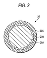
- the magnetic solder balls 20 has a structure in which a solder-diffusion barrier layer 20B and a solder layer 20C are sequentially provided around a core 20A formed of Cu, a resin, or the like. Since the solder-diffusion barrier layer 20 is formed of a ferromagnetic material such as Ni, the solder ball 20 as a whole exhibits a magnetic property.
- the magnet 104 in the stage 102 is moved in the direction of arrow M in parallel with the lower surface of the substrate 10 to cause the magnetic solder balls 20 dispersed on the mask 18 to move on the mask 18 by the action of the magnetic force from the magnet 104, thereby dropping the magnetic solder balls 20 into the openings 22 of the mask 18 so as to mount the magnetic solder balls 20 on the bonding pads 16 located below the openings 22.
- the magnet 104 may be a permanent magnet or an electromagnet.
- the solder balls can be arranged on the necessary bonding pads over the entire region of the substrate.
- a vertically moving mechanism may be provided for shielding the magnetic force which is directed in the upward direction.
- An arranging apparatus 150 is comprised of a stage 102 for placing and fixing the substrate 10 thereon; the mask frame 106 capable of being positioned above the stage 102; and a magnetic head 110 serving as a magnetic generator which is movable above the mask frame 106 and causes a magnetic force to act on the stage 102.
- the arranging apparatus 150 is an apparatus for arranging the magnetic solder balls 20 one each on each of the plurality of bonding pads 16 on the substrate 10 through the mask 18.
- the substrate 10 is a multilayered circuit board in which a wiring layer and an insulating layer are laminated on both surfaces of a resin-made core substrate having through holes and the like by means of the build-up process or the like.
- the solder resist layer 14 is formed on each of both upper and lower surfaces of the multilayered circuit portion 12, and the multiplicity of bonding pads 16 arranged on the upper surface of the multilayered circuit portion 12 are exposed in the openings of the solder resist layer 14.
- the substrate 10 with the adhesive flux 17 coated on the bonding pads 16 is placed and fixed on the stage 102.
- the stage 102 sucks and fixes the substrate 10 by air suction from the suction ports 108.
- the mask frame 106 to which the mask 18 having openings 22 corresponding to the positions of the bonding pads 16 of the substrate 10 is affixed, is disposed and made stationary on the substrate 10 with a predetermined interval provided between the mask 18 and the substrate 10, such that the bonding pads 16 and the openings are positioned with respect to each other.
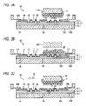
- the magnetic head 110 which attracted the magnetic solder balls 20 by the magnetic force is stopped above a predetermined solder-ball arrangement area of the substrate 10, and the attracting operation of the magnetic head 110 is stopped, as shown in Fig. 3B , so as to disperse the magnetic solder balls 20 on the mask 18, thereby dropping the solder balls 20 into the openings 22 of the mask 18 and mounting the solder balls 20 on the bonding pads 16 located below the openings 22.
- the magnetic head 110 is a magnetic generator which is capable of starting and stopping the attracting operation, as described above, and typically employs an electromagnet.
- the magnetic head 110 is not necessarily limited to the electromagnet, and it is also possible to adopt a form in which a permanent magnet is used, as shown in Fig. 4 .
- the magnetic head 110 shown in Fig. 4 has a permanent magnet 110A and a bulkhead 110B formed of a ferromagnetic material.
- the permanent magnet 110A is moved vertically in the direction of arrow Y, it is possible to adjust the interval with the ferromagnetic bulkhead 110B to thereby increase or decrease the magnetization of the ferromagnetic bulkhead 110B and increase or decrease the magnetic force acting in the magnetic solder balls 20, thereby making it possible to start and stop the attracting operation as the magnetic head 110.
- the attracting operation of the magnetic head 110 is resumed, and excess magnetic solder balls 20 on the mask 18 are attracted by the magnetic head 110 and are removed from the mask 18.
- the magnetic head 110 which is attracting the magnetic solder balls 20 is moved in the direction of the arrow M and is stopped in an ensuing predetermined solder-ball arrangement area, and the operation shown in Figs. 3A and 3B is repeated.
- the solder balls can be arranged on the necessary bonding pads over the entire region of the substrate.
- the magnetic head in accordance with the second embodiment may have a vibrating mechanism for causing the solder balls to drop efficiently.
- the bulkhead provided between the magnetic head and the mask in the second embodiment may have the vibrating mechanism.
- the magnetic head used in the second embodiment may be used to remove excess solder balls from the dropping device used in the first embodiment.
- the material of the mask may be a soft magnetic material such as Fe, but may be a resin or the like.
- as a method of application of the flux it is possible to use a printing process, a dispensing process, a transfer process, and the like.
- an apparatus and a method for arranging magnetic solder balls are provided which make it possible to dispose on bonding pads of a substrate infinitesimally small solder balls, particularly magnetic cored solder balls, without causing damage to, deformation of, and commingling of foreign matter with, the solder balls, which have been unavoidable with the conventional dropping means using such as a spatula or brush.
Landscapes
- Engineering & Computer Science (AREA)
- Manufacturing & Machinery (AREA)
- Microelectronics & Electronic Packaging (AREA)
- Mechanical Engineering (AREA)
- Electric Connection Of Electric Components To Printed Circuits (AREA)
Abstract
Description
- The present invention relates to an apparatus and a method for arranging magnetic solder balls. In particular, it relates to an apparatus and a method for arranging the magnetic solder balls one each on each of a plurality of bonding pads on a substrate, more particularly through a mask.
- Conventionally, solder paste is screen printed to form solder bumps on bonding pads for flip chip bonding of a substrate such as a wafer or a circuit substrate. However, in conjunction with the trend toward the higher density of semiconductor devices, the bump pitch is required to be infinitesimally small such as on the order of 200 m or even 150 m. If solder paste is screen printed at such an infinitesimally small pitch, attachment of the solder paste on a bridge between bumps and on a screen mask occurs. For this reason, the formation of the solder bumps at the infinitesimally small pitch cannot be effected by screen printing.
- Accordingly, as a method of forming bumps at an infinitesimally small pitch, it is conceivable to arrange the solder balls on the bonding pads.
- As one method which is conventionally carried out for bonding pads for board mounting on the outer side of a ball grid array (BGA), a method is known in which solder balls are sucked by a sucking jig and are transported so as to be mounted on the bonding pads. Adhesive soldering flux is coated in advance on the bonding pads, to thereby allow the solder balls to adhere to and fixed to the bonding pads. In this case, however, the diameter of the solder balls is large in the vicinities of 0.5 to 0.7 mm. In contrast, the diameter of the solder balls for the infinitesimally small pitch needs to be set to 100 m or below. When the solder balls thus become infinitesimally small, there arise problems that the solder balls coagulate due to the action of static electric charge, and that the solder balls cannot be disposed at accurate positions owing to the effect of air flow. In addition, suction ports of the suction jig are also miniaturized, so that the processing cost becomes high, which is not suitable for practical use.
- For this reason, a method in which the solder balls are dropped into openings of the mask placed on the substrate (a so-called "dropping method") is carried out as another method. After the application of flux to the bonding pads on the substrate, the pads and the metal mask are positioned and superposed on top of each other. In that state, the solder balls are dropped from above the metal mask, and the solder balls are dropped into the openings of the metal mask. The solder balls are dropped from a container having an opening such as a slit, and it is ensured that an appropriate amount is dropped onto the mask. One ball is dropped into each opening of the mask, is placed on the bonding pad positioned with respect to the opening, and is adhered and fixed by adhesive flux applied to the bonding pad. The solder balls remaining on the mask are collected by a collecting mechanism.
- Here, a means for reliably dropping the solder balls into the mask openings should preferably be provided. Patent document 1 discloses a method in which, by using a flexible spatula or brush as a dropping means, the solder balls are mechanically moved forcibly on the mask to drop the solder balls into the mask openings.
- However, if the mechanical forcible movement by means of the spatula or the brush is carried out, there arise problems in that damage or deformation can occur in the solder balls owing to the spatula or the brush, and that foreign matter can be mixed in from the brush.
- In recent years, cored solder balls such as Cu-cored solder balls and resin-cored solder balls have been used. The cored solder ball has a structure in which a solder layer is provided on the surface of a Cu or resin core, and a diffusion barrier layer is interposed between the core and the solder layer so that the solder in the surface layer is not diffused into the core under a high temperature during flip chip bonding. Here, the diffusion barrier layer is formed of a ferromagnetic material such as Ni.
- This cored solder ball has outstanding advantages in that even if the solder is fused at the time of flip chip bonding, the Cu or resin core keeps its original shape and functions as a spacer for keeping a constant interval between an electronic part such as a semiconductor device and a mounting substrate and prevents faulty connection due to the cracking or deformation of the solder bump caused by high-temperature degradation.
- However, if the mechanical forcible movement by means of the spatula or the brush is carried out, damage, deformation, and commingling of foreign matter due to it can occur, so that there has been a problem that full use cannot be made of the outstanding advantages of the cored solder balls.
- Patent Document 1 is
JP-A-2004-311886 - The present invention intends to overcome at least some of the above problems. The object is solved by the apparatuses for arranging magnetic solder balls according to claim 1 and 5, and by the methods of claims 3 and 8. Further advantages, features, aspects and details of the invention are evident from the dependent claims, the description and the drawings.
An advantage of the apparatus and the method according to the invention is that they allow to dispose on bonding pads of a substrate infinitesimally small solder balls, particularly magnetic cored solder balls, without causing damage to, deformation of, and commingling of foreign matter with, the solder balls, which have been unavoidable with a conventional dropping means. - According to a first aspect of the invention, there is provided an apparatus for arranging magnetic solder balls, and more particularly for arranging them one each on each of a plurality of bonding pads on a substrate through a mask, including: a stage for placing and fixing the substrate thereon; a magnet which is incorporated in the stage and is movable in parallel with a lower surface of the placed and fixed substrate so as to cause a magnetic force to act in an upward direction of the stage; and a mask frame capable of being positioned above the stage. An arranging method using this arranging apparatus is also provided.
- Further, according to a second aspect of the invention, there is provided a method for arranging magnetic solder balls one each on each of a plurality of bonding pads on a substrate through a mask by using the apparatus according to the first aspect, including the steps of:
- placing and fixing on the stage the substrate with adhesive flux coated on the bonding pads;
- causing the mask frame, to which the mask having openings corresponding to positions of the bonding pads of the substrate is affixed, to be disposed on the substrate with a predetermined interval provided between the mask and the substrate, such that the bonding pads and the openings are positioned with respect to each other;
- dispersing the magnetic solder balls on the mask; and
- moving the magnet in the stage in parallel with the lower surface of the substrate to cause the magnetic solder balls dispersed on the mask to move on the mask by the action of a magnetic force from the magnet, to drop the magnetic solder balls into the openings of the mask so that the magnetic solder balls are mounted on the bonding pads located below the openings.
- Further, according to a third aspect of the invention, there is provided an apparatus for arranging magnetic solder balls, and more particularly for arranging them one each on each of a plurality of bonding pads on a substrate through a mask, including: a stage for placing and fixing the substrate thereon; a mask frame capable of being positioned above the stage; and a magnetic generator which is movable above the mask frame and causes a magnetic force to act on the stage. An arranging method using this arranging apparatus is also provided.
Further, according to a forth aspect of the invention, there is provided the apparatus for arranging magnetic solder balls according to the third aspect, further including: - a bulkhead formed of a ferromagnetic material and disposed between the mask frame and the magnetic generator formed of a permanent magnet.
- Further, according to a fifth aspect of the invention, there is provided a method for arranging magnetic solder balls one each on each of a plurality of bonding pads on a substrate through a mask by using the apparatus according to the third or forth aspect, including the steps of: placing and fixing on the stage the substrate with adhesive flux coated on the bonding pads; causing the mask frame, to which the mask having openings corresponding to positions of the bonding pads of the substrate is affixed, to be disposed on the substrate with a predetermined interval provided between the mask and the substrate, such that the bonding pads and the openings are positioned with respect to each other; and causing the magnetic generator which attracts the magnetic solder balls by the magnetic force to be stopped above a predetermined solder-ball arrangement area of the substrate, and stopping the attracting operation of the magnetic generator, so as to disperse the magnetic solder balls on the mask, to drop the solder balls into the openings of the mask so that the solder balls are mounted on the bonding pads located below the openings.
- According to the first invention of the invention, the magnet incorporated in the stage with the substrate placed and fixed thereon is used as a dropping means, and the magnetic solder balls are moved on the mask by moving the magnet below the stage while a magnetic force is being applied to the magnetic solder balls on the mask located above the stage, thereby dropping the magnetic solder balls into the openings of the mask so as to mount the magnetic solder balls on the bonding pads located below the openings. Therefore, the magnetic solder balls can be dropped in a mechanically non-contacting state. Hence, it is possible to prevent the occurrence of the damage to, deformation of, and commingling of foreign matter with, the solder balls, which unavoidably occurred in the dropping based on the mechanical contact using a conventional spatula or brush as the dropping means.
- According to the second invention of the invention, the magnetic generator which attracted the magnetic solder balls by the magnetic force is stopped above a predetermined solder-ball arrangement area of the substrate, and the attracting operation of the magnetic generator is stopped, so as to disperse the magnetic solder balls on the mask, thereby dropping the solder balls into the openings of the mask and mounting the solder balls on the bonding pads located below the openings. Therefore, the magnetic solder balls can be dropped in a mechanically non-contacting state. Hence, it is possible to prevent the occurrence of the damage to, deformation of, and commingling of foreign matter with, the solder balls, which unavoidably occurred in the dropping based on the mechanical contact using a conventional spatula or brush as the dropping means.
The invention is also directed to apparatuses for carrying out the disclosed methods and including apparatus parts for performing each described method steps. These method steps may be performed by way of hardware components, a computer programmed by appropriate software, by any combination of the two or in any other manner. Furthermore, the invention is also directed to methods by which the described apparatus operates. It includes method steps for carrying out every function of the apparatus or manufacturing every part of the apparatus. - The invention will be better understood by reference to the following description of embodiments of the invention taken in conjunction with the accompanying drawings, wherein:
-
Fig. 1A is a cross-sectional view illustrating an apparatus for arranging magnetic solder balls in accordance with a first embodiment of the invention; -
Fig. 1B is a plan view of the apparatus for arranging magnetic solder balls in accordance with the first embodiment of the invention; -
Fig. 2 is a cross-sectional view illustrating an example of the structure of a magnetic solder ball; -
Figs. 3A to 3C are cross-sectional views illustrating an apparatus and a method for arranging magnetic solder balls in accordance with a second embodiment of the invention; and -
Fig. 4 is a cross-sectional view illustrating another example of a magnetic head in accordance with the second embodiment of the invention. - Referring to
Figs. 1A and 1B , a description will be given of an apparatus for arranging magnetic solder balls in accordance with the invention.Fig. 1A is a cross-sectional view, andFig. 1B is a plan view. - An arranging
apparatus 100 is comprised of astage 102 for placing and fixing asubstrate 10 thereon;magnets 104 which are incorporated in thestage 102 and are movable in parallel with the lower surface of the placed and fixedsubstrate 10 so as to cause a magnetic force to act in the upward direction of thestage 102; and amask frame 106 capable of being positioned above thestage 102. The arrangingapparatus 100 is an apparatus for arrangingmagnetic solder balls 20 one each on each of a plurality ofbonding pads 16 on thesubstrate 10 through amask 18. - The
substrate 10 is a multilayered circuit board in which a wiring layer and an insulating layer are laminated on both surfaces of a resin-made core substrate having through holes and the like by means of the build-up process or the like. A solder resistlayer 14 is formed on each of both upper and lower surfaces of amultilayered circuit portion 12, and the multiplicity ofbonding pads 16 arranged on an upper surface of themultilayered circuit portion 12 are exposed in openings of the solder resistlayer 14. - It should be noted that although, for the convenience of description, a description will be given of the case where the
bonding pads 16 are arranged only on one surface of thesubstrate 10, also in the case where thebonding pads 16 are arranged on both surfaces of thesubstrate 10 it suffices if each operation described below is carried out for the both surfaces in a similar manner. - A description will be given below of a method of arranging the magnetic solder balls by using the arranging
apparatus 100. - The
substrate 10 withadhesive flux 17 coated on thebonding pads 16 is placed and fixed on thestage 102. Thestage 102 sucks and fixes thesubstrate 10 by air suction fromsuction ports 108. - The
mask frame 106, to which themask 18 havingopenings 22 corresponding to the positions of thebonding pads 16 of thesubstrate 10 is affixed, is disposed and made stationary on thesubstrate 10 with a predetermined interval provided between themask 18 and thesubstrate 10, such that thebonding pads 16 and the openings are positioned with respect to each other. - The
magnetic solder balls 20 are dispersed on themask 18. Themagnetic solder balls 20 is a cored solder ball such as a Cu-cored solder ball or a resin-cored solder ball. As shown inFig. 2 , themagnetic solder balls 20 has a structure in which a solder-diffusion barrier layer 20B and asolder layer 20C are sequentially provided around acore 20A formed of Cu, a resin, or the like. Since the solder-diffusion barrier layer 20 is formed of a ferromagnetic material such as Ni, thesolder ball 20 as a whole exhibits a magnetic property. - The
magnet 104 in thestage 102 is moved in the direction of arrow M in parallel with the lower surface of thesubstrate 10 to cause themagnetic solder balls 20 dispersed on themask 18 to move on themask 18 by the action of the magnetic force from themagnet 104, thereby dropping themagnetic solder balls 20 into theopenings 22 of themask 18 so as to mount themagnetic solder balls 20 on thebonding pads 16 located below theopenings 22. Themagnet 104 may be a permanent magnet or an electromagnet. - As the above-described operation is sequentially repeated with respect to the remaining predetermined solder-ball arrangement areas, the solder balls can be arranged on the necessary bonding pads over the entire region of the substrate.
- It is thus the magnetic force from the
magnet 104 that directly acts on themagnetic solder balls 20 as a dropping means. Since a spatula or a brush is not directly brought into mechanical contact with the solder balls as in the case of the conventional dropping means, damage to, deformation of, and commingling of foreign matter with, thesolder balls 20 owing to the dropping means do not occur. - In the first embodiment, in the case where the magnets which are incorporated in the stage are permanent magnets, a vertically moving mechanism may be provided for shielding the magnetic force which is directed in the upward direction.
- Referring to
Fig. 3 , a description will be given of the apparatus for arranging magnetic solder balls in accordance with the second invention. - An arranging
apparatus 150 is comprised of astage 102 for placing and fixing thesubstrate 10 thereon; themask frame 106 capable of being positioned above thestage 102; and amagnetic head 110 serving as a magnetic generator which is movable above themask frame 106 and causes a magnetic force to act on thestage 102. The arrangingapparatus 150 is an apparatus for arranging themagnetic solder balls 20 one each on each of the plurality ofbonding pads 16 on thesubstrate 10 through themask 18. - The
substrate 10 is a multilayered circuit board in which a wiring layer and an insulating layer are laminated on both surfaces of a resin-made core substrate having through holes and the like by means of the build-up process or the like. The solder resistlayer 14 is formed on each of both upper and lower surfaces of themultilayered circuit portion 12, and the multiplicity ofbonding pads 16 arranged on the upper surface of themultilayered circuit portion 12 are exposed in the openings of the solder resistlayer 14. - It should be noted that although, for the convenience of description, a description will be given of the case where the
bonding pads 16 are arranged only on one surface of thesubstrate 10, in the case where thebonding pads 16 are arranged on both surfaces of thesubstrate 10 it suffices if each operation described below is similarly carried out for the both surfaces. - A description will be given below of a method of arranging the magnetic solder balls by using the arranging
apparatus 150. - As shown in
Fig. 3A , thesubstrate 10 with theadhesive flux 17 coated on thebonding pads 16 is placed and fixed on thestage 102. Thestage 102 sucks and fixes thesubstrate 10 by air suction from thesuction ports 108. - The
mask frame 106, to which themask 18 havingopenings 22 corresponding to the positions of thebonding pads 16 of thesubstrate 10 is affixed, is disposed and made stationary on thesubstrate 10 with a predetermined interval provided between themask 18 and thesubstrate 10, such that thebonding pads 16 and the openings are positioned with respect to each other. - The
magnetic head 110 which attracted themagnetic solder balls 20 by the magnetic force is stopped above a predetermined solder-ball arrangement area of thesubstrate 10, and the attracting operation of themagnetic head 110 is stopped, as shown inFig. 3B , so as to disperse themagnetic solder balls 20 on themask 18, thereby dropping thesolder balls 20 into theopenings 22 of themask 18 and mounting thesolder balls 20 on thebonding pads 16 located below theopenings 22. Themagnetic head 110 is a magnetic generator which is capable of starting and stopping the attracting operation, as described above, and typically employs an electromagnet. However, themagnetic head 110 is not necessarily limited to the electromagnet, and it is also possible to adopt a form in which a permanent magnet is used, as shown inFig. 4 . - Namely, the
magnetic head 110 shown inFig. 4 has apermanent magnet 110A and abulkhead 110B formed of a ferromagnetic material. As thepermanent magnet 110A is moved vertically in the direction of arrow Y, it is possible to adjust the interval with theferromagnetic bulkhead 110B to thereby increase or decrease the magnetization of theferromagnetic bulkhead 110B and increase or decrease the magnetic force acting in themagnetic solder balls 20, thereby making it possible to start and stop the attracting operation as themagnetic head 110. - After the dropping of the
magnetic solder balls 20 is finished, the attracting operation of themagnetic head 110 is resumed, and excessmagnetic solder balls 20 on themask 18 are attracted by themagnetic head 110 and are removed from themask 18. Themagnetic head 110 which is attracting themagnetic solder balls 20 is moved in the direction of the arrow M and is stopped in an ensuing predetermined solder-ball arrangement area, and the operation shown inFigs. 3A and 3B is repeated. - As the above-described operation is sequentially repeated with respect to the remaining predetermined solder-ball arrangement areas, the solder balls can be arranged on the necessary bonding pads over the entire region of the substrate.
- In this embodiment as well, it is the magnetic force from the
magnet 104 that directly acts on themagnetic solder balls 20 as the dropping means. Since a spatula or a brush is not directly brought into mechanical contact with the solder balls as in the case of the conventional dropping means, damage to, deformation of, and commingling of foreign matter with, thesolder balls 20 owing to the dropping means do not occur. - The magnetic head in accordance with the second embodiment may have a vibrating mechanism for causing the solder balls to drop efficiently.
The bulkhead provided between the magnetic head and the mask in the second embodiment may have the vibrating mechanism. - The magnetic head used in the second embodiment may be used to remove excess solder balls from the dropping device used in the first embodiment.
In the invention, the material of the mask may be a soft magnetic material such as Fe, but may be a resin or the like.
In the invention, as a method of application of the flux, it is possible to use a printing process, a dispensing process, a transfer process, and the like. - According to the invention, an apparatus and a method for arranging magnetic solder balls are provided which make it possible to dispose on bonding pads of a substrate infinitesimally small solder balls, particularly magnetic cored solder balls, without causing damage to, deformation of, and commingling of foreign matter with, the solder balls, which have been unavoidable with the conventional dropping means using such as a spatula or brush.
Claims (9)
- An apparatus (100) for arranging magnetic solder balls (20) on a plurality of bonding pads (16) on a substrate (10) through a mask (18), comprising:a stage (102) for placing and fixing the substrate (10) thereon;a magnet (104) which is movable in parallel with a lower surface of the placed and fixed substrate so as to cause a magnetic force to act in an upward direction of the stage (102); anda mask frame (106) capable of being positioned above the stage (102).
- The apparatus of claim 1, being an apparatus (100) for arranging the magnetic solder balls (20) one each on each of the plurality of bonding pads (16), wherein the magnet (104) is incorporated in the stage.
- A method for arranging magnetic solder balls (20) on a plurality of bonding pads (16) on a substrate (10), preferably one solder ball (20) each on each of the plurality of bonding pads (16), through a mask by using the apparatus (100) according to claim 1 or 2.
- The method of claim 3, further comprising the steps of:placing and fixing on the stage (102) the substrate with adhesive flux (17) coated on the bonding pads (16);causing the mask frame (106), to which the mask (18) having openings (22) corresponding to positions of the bonding pads (16) of the substrate is affixed, to be disposed on the substrate with a predetermined interval provided between the mask (18) and the substrate (10), such that the bonding pads (16) and the openings (22) are positioned with respect to each other;dispersing the magnetic solder balls (20) on the mask (18); andmoving the magnet (104) in the stage (102) in parallel with the lower surface of the substrate to cause the magnetic solder balls dispersed on the mask to move on the mask by the action of a magnetic force from the magnet, to drop the magnetic solder balls into the openings of the mask so that the magnetic solder balls are mounted on the bonding pads located below the openings.
- An apparatus (100) for arranging magnetic solder balls (20) on a plurality of bonding pads (16) on a substrate (10) through a mask (18), comprising:a stage (102) for placing and fixing the substrate (10) thereon;a mask frame (106) capable of being positioned above the stage (102); anda magnetic generator (110) which is movable above the mask frame (106) and is adapted to cause a magnetic force to act on the stage (102).
- The apparatus of claim 5, being an apparatus (100) for arranging the magnetic solder balls (20) one each on each of the plurality of bonding pads (16).
- The apparatus for arranging magnetic solder balls according to claim 6 or 7, further comprising:a bulkhead (110B) formed of a ferromagnetic material and disposed between the mask frame (106) and the magnetic generator (110) formed of a permanent magnet.
- A method for arranging magnetic solder balls on a plurality of bonding pads (16) on a substrate (10), preferably one solder ball (20) each on each of the plurality of bonding pads (16), through a mask by using the apparatus according to one of the claims 5 to 7.
- The method of claim 8, comprising the steps of:placing and fixing on the stage the substrate with adhesive flux coated on the bonding pads;causing the mask frame, to which the mask having openings corresponding to positions of the bonding pads of the substrate is affixed, to be disposed on the substrate with a predetermined interval provided between the mask and the substrate, such that the bonding pads and the openings are positioned with respect to each other; andcausing the magnetic generator which attracts the magnetic solder balls by the magnetic force to be stopped above a predetermined solder-ball arrangement area of the substrate, andstopping the attracting operation of the magnetic generator, so as to disperse the magnetic solder balls on the mask, to drop the solder balls into the openings of the mask so that the solder balls are mounted on the bonding pads located below the openings.
Applications Claiming Priority (1)
| Application Number | Priority Date | Filing Date | Title |
|---|---|---|---|
| JP2007193643A JP4393538B2 (en) | 2007-07-25 | 2007-07-25 | Magnetic solder ball arrangement apparatus and arrangement method |
Publications (2)
| Publication Number | Publication Date |
|---|---|
| EP2019422A2 true EP2019422A2 (en) | 2009-01-28 |
| EP2019422A3 EP2019422A3 (en) | 2013-07-03 |
Family
ID=39874076
Family Applications (1)
| Application Number | Title | Priority Date | Filing Date |
|---|---|---|---|
| EP08161117.0A Withdrawn EP2019422A3 (en) | 2007-07-25 | 2008-07-24 | Apparatus and method for arranging magnetic solder balls |
Country Status (3)
| Country | Link |
|---|---|
| US (2) | US7784671B2 (en) |
| EP (1) | EP2019422A3 (en) |
| JP (1) | JP4393538B2 (en) |
Cited By (3)
| Publication number | Priority date | Publication date | Assignee | Title |
|---|---|---|---|---|
| CN105405780A (en) * | 2015-12-16 | 2016-03-16 | 华进半导体封装先导技术研发中心有限公司 | Wafer ball-mounting process adopting template-free method |
| CN105489514A (en) * | 2015-12-16 | 2016-04-13 | 华进半导体封装先导技术研发中心有限公司 | Template-free wafer bumping process |
| CN107877018A (en) * | 2017-10-24 | 2018-04-06 | 杭州华光焊接新材料股份有限公司 | A kind of induced by magnetic field welding method |
Families Citing this family (25)
| Publication number | Priority date | Publication date | Assignee | Title |
|---|---|---|---|---|
| WO2006098187A1 (en) * | 2005-03-15 | 2006-09-21 | Matsushita Electric Industrial Co., Ltd. | Flip chip mounting method and bump forming method |
| US7651021B2 (en) * | 2007-12-28 | 2010-01-26 | Intel Corporation | Microball attachment using self-assembly for substrate bumping |
| US7780063B2 (en) * | 2008-05-15 | 2010-08-24 | International Business Machines Corporation | Techniques for arranging solder balls and forming bumps |
| JP5310252B2 (en) * | 2009-05-19 | 2013-10-09 | パナソニック株式会社 | Electronic component mounting method and electronic component mounting structure |
| JP5303489B2 (en) * | 2010-02-16 | 2013-10-02 | ルネサスエレクトロニクス株式会社 | Manufacturing method of semiconductor device |
| US20110244145A1 (en) * | 2010-03-31 | 2011-10-06 | Shiuan-Sheng Wang | Iron particulate-reinforced tin based matrix composite solder ball and flip chip ball placement method using same |
| US8939347B2 (en) | 2010-04-28 | 2015-01-27 | Intel Corporation | Magnetic intermetallic compound interconnect |
| US9847308B2 (en) | 2010-04-28 | 2017-12-19 | Intel Corporation | Magnetic intermetallic compound interconnect |
| US8313958B2 (en) * | 2010-05-12 | 2012-11-20 | Intel Corporation | Magnetic microelectronic device attachment |
| US8434668B2 (en) | 2010-05-12 | 2013-05-07 | Intel Corporation | Magnetic attachment structure |
| US8609532B2 (en) | 2010-05-26 | 2013-12-17 | Intel Corporation | Magnetically sintered conductive via |
| KR102084696B1 (en) * | 2013-01-23 | 2020-03-05 | 삼성디스플레이 주식회사 | Thin layer deposition apparatus for display device, mask unit for depositing thin layer in display device, display device and method of manufacturing the same |
| KR102029077B1 (en) | 2013-02-04 | 2019-10-07 | 삼성전자주식회사 | Method of forming external terminals of a package and apparatus for performing the same |
| JP6109609B2 (en) * | 2013-03-14 | 2017-04-05 | Aiメカテック株式会社 | Solder ball printing machine and solder ball printing method |
| US9721855B2 (en) * | 2014-12-12 | 2017-08-01 | International Business Machines Corporation | Alignment of three dimensional integrated circuit components |
| CN105470145B (en) * | 2015-12-16 | 2017-11-24 | 华进半导体封装先导技术研发中心有限公司 | Ball technique is planted without the double roller bearing wafers of template |
| US20170179069A1 (en) * | 2015-12-18 | 2017-06-22 | Jonathon R. Carstens | Ball grid array solder attachment |
| US10576566B2 (en) | 2016-06-06 | 2020-03-03 | International Business Machines Corporation | Solder paste misprint cleaning |
| US9905525B1 (en) * | 2016-08-18 | 2018-02-27 | Semiconductor Components Industries, Llc | Semiconductor wafer and method of ball drop on thin wafer with edge support ring |
| US12543270B2 (en) | 2017-11-15 | 2026-02-03 | SunRay Scientific, Inc. | Method for creating interconnections between a substrate and electronic components |
| WO2019099754A1 (en) * | 2017-11-15 | 2019-05-23 | Sunray Scientific, Llc | System and method for improved electronic component interconnections |
| KR102078935B1 (en) * | 2018-11-07 | 2020-02-19 | 주식회사 프로텍 | Apparatus for Mounting Conductive Ball |
| KR102078936B1 (en) * | 2018-11-07 | 2020-02-19 | 주식회사 프로텍 | Method of Mounting Conductive Ball |
| KR102330427B1 (en) * | 2020-06-03 | 2021-11-24 | 주식회사 프로텍 | Method of Mounting Conductive Ball Using Electrostatic Chuck |
| CN113948624B (en) * | 2020-07-16 | 2023-10-24 | 重庆康佳光电技术研究院有限公司 | LED solder coating method, light-emitting device and display device |
Citations (1)
| Publication number | Priority date | Publication date | Assignee | Title |
|---|---|---|---|---|
| JP2004311886A (en) | 2003-04-10 | 2004-11-04 | Hitachi Metals Ltd | Apparatus and method for mounting conductive ball |
Family Cites Families (6)
| Publication number | Priority date | Publication date | Assignee | Title |
|---|---|---|---|---|
| JPH07283521A (en) | 1994-04-06 | 1995-10-27 | Fujitsu Ltd | Forming solder mounting method |
| JPH08236529A (en) * | 1995-02-28 | 1996-09-13 | Matsushita Electric Works Ltd | Solder ball, solder bump, semiconductor device, method of forming the solder bump, and method of mounting the semiconductor device |
| TWI285524B (en) * | 2003-03-10 | 2007-08-11 | Hitachi Metals Ltd | Method and apparatus for carrying electric conductive ball |
| JP4348696B2 (en) | 2004-06-21 | 2009-10-21 | 日立金属株式会社 | Conductive ball array mask and array device using the same |
| JP2007090188A (en) * | 2005-09-28 | 2007-04-12 | Hitachi Metals Ltd | Printing material coating method and printing material coating apparatus |
| JP2007125794A (en) | 2005-11-04 | 2007-05-24 | Hitachi Metals Ltd | Screen printing apparatus and screen printing method |
-
2007
- 2007-07-25 JP JP2007193643A patent/JP4393538B2/en not_active Expired - Fee Related
-
2008
- 2008-07-23 US US12/178,102 patent/US7784671B2/en not_active Expired - Fee Related
- 2008-07-24 EP EP08161117.0A patent/EP2019422A3/en not_active Withdrawn
-
2010
- 2010-07-09 US US12/833,191 patent/US7854367B2/en not_active Expired - Fee Related
Patent Citations (1)
| Publication number | Priority date | Publication date | Assignee | Title |
|---|---|---|---|---|
| JP2004311886A (en) | 2003-04-10 | 2004-11-04 | Hitachi Metals Ltd | Apparatus and method for mounting conductive ball |
Cited By (5)
| Publication number | Priority date | Publication date | Assignee | Title |
|---|---|---|---|---|
| CN105405780A (en) * | 2015-12-16 | 2016-03-16 | 华进半导体封装先导技术研发中心有限公司 | Wafer ball-mounting process adopting template-free method |
| CN105489514A (en) * | 2015-12-16 | 2016-04-13 | 华进半导体封装先导技术研发中心有限公司 | Template-free wafer bumping process |
| CN105489514B (en) * | 2015-12-16 | 2017-11-24 | 华进半导体封装先导技术研发中心有限公司 | Ball technique is planted without template wafer |
| CN105405780B (en) * | 2015-12-16 | 2017-11-24 | 华进半导体封装先导技术研发中心有限公司 | The wafer of template-free method plants ball technique |
| CN107877018A (en) * | 2017-10-24 | 2018-04-06 | 杭州华光焊接新材料股份有限公司 | A kind of induced by magnetic field welding method |
Also Published As
| Publication number | Publication date |
|---|---|
| JP4393538B2 (en) | 2010-01-06 |
| US20090072012A1 (en) | 2009-03-19 |
| JP2009032813A (en) | 2009-02-12 |
| EP2019422A3 (en) | 2013-07-03 |
| US20100270364A1 (en) | 2010-10-28 |
| US7784671B2 (en) | 2010-08-31 |
| US7854367B2 (en) | 2010-12-21 |
Similar Documents
| Publication | Publication Date | Title |
|---|---|---|
| US7784671B2 (en) | Apparatus and method for arranging magnetic solder balls | |
| US7820479B2 (en) | Conductive ball mounting method | |
| JP4503053B2 (en) | Conductive ball mounting apparatus and mounting method | |
| US8671561B2 (en) | Substrate manufacturing method | |
| KR20080037551A (en) | Solder Ball Mounting Method and Manufacturing Method of Solder Ball Mounting Substrate | |
| JP6138019B2 (en) | Electrode forming apparatus, electrode forming system, and electrode forming method | |
| EP0962969A2 (en) | Method for forming bumps | |
| KR100983253B1 (en) | Mounting method and mounting apparatus of conductive ball | |
| JP4271241B2 (en) | Micro ball mounting device | |
| US6946601B1 (en) | Electronic package with passive components | |
| US6869008B2 (en) | Method of forming bumps | |
| JP2010177253A (en) | Solder ball loading method | |
| KR101128645B1 (en) | Mask frame apparatus for solder ball mounting | |
| JP4313814B2 (en) | Solder ball mounting method and solder ball mounting apparatus | |
| JP5121621B2 (en) | Substrate manufacturing method | |
| JP2003266629A (en) | Printing method, printing apparatus, and semiconductor device | |
| JP4974818B2 (en) | Substrate manufacturing method and substrate manufacturing apparatus | |
| WO2010100706A1 (en) | Semiconductor device | |
| JP3015470B2 (en) | Solder bump forming method and mask fixing magnet | |
| JP4849136B2 (en) | Mounting method of conductive balls | |
| JP7109076B2 (en) | Substrate adsorption/fixation stage and ball mounting device | |
| JP2004311886A (en) | Apparatus and method for mounting conductive ball | |
| JP2001103418A (en) | Manufacturing method of electronic components | |
| JP2024107578A (en) | Ball mounting device and ball mounting method | |
| JP2025023582A (en) | Method for forming solder bumps |
Legal Events
| Date | Code | Title | Description |
|---|---|---|---|
| PUAI | Public reference made under article 153(3) epc to a published international application that has entered the european phase |
Free format text: ORIGINAL CODE: 0009012 |
|
| AK | Designated contracting states |
Kind code of ref document: A2 Designated state(s): AT BE BG CH CY CZ DE DK EE ES FI FR GB GR HR HU IE IS IT LI LT LU LV MC MT NL NO PL PT RO SE SI SK TR |
|
| AX | Request for extension of the european patent |
Extension state: AL BA MK RS |
|
| RIC1 | Information provided on ipc code assigned before grant |
Ipc: H05K 3/34 20060101ALI20130201BHEP Ipc: B23K 3/06 20060101AFI20130201BHEP Ipc: H01L 21/48 20060101ALI20130201BHEP |
|
| PUAL | Search report despatched |
Free format text: ORIGINAL CODE: 0009013 |
|
| RIN1 | Information on inventor provided before grant (corrected) |
Inventor name: IIDA, KIYOAKI Inventor name: SAKAGUCHI, HIDEAKI |
|
| AK | Designated contracting states |
Kind code of ref document: A3 Designated state(s): AT BE BG CH CY CZ DE DK EE ES FI FR GB GR HR HU IE IS IT LI LT LU LV MC MT NL NO PL PT RO SE SI SK TR |
|
| AX | Request for extension of the european patent |
Extension state: AL BA MK RS |
|
| RIC1 | Information provided on ipc code assigned before grant |
Ipc: B23K 3/06 20060101AFI20130527BHEP Ipc: H01L 21/48 20060101ALI20130527BHEP Ipc: H05K 3/34 20060101ALI20130527BHEP |
|
| AKY | No designation fees paid | ||
| REG | Reference to a national code |
Ref country code: DE Ref legal event code: R108 |
|
| REG | Reference to a national code |
Ref country code: DE Ref legal event code: R108 Effective date: 20140312 |
|
| STAA | Information on the status of an ep patent application or granted ep patent |
Free format text: STATUS: THE APPLICATION IS DEEMED TO BE WITHDRAWN |
|
| 18D | Application deemed to be withdrawn |
Effective date: 20140104 |