EP2017743A2 - High speed and efficient matrix multiplication hardware module - Google Patents
High speed and efficient matrix multiplication hardware module Download PDFInfo
- Publication number
- EP2017743A2 EP2017743A2 EP08159750A EP08159750A EP2017743A2 EP 2017743 A2 EP2017743 A2 EP 2017743A2 EP 08159750 A EP08159750 A EP 08159750A EP 08159750 A EP08159750 A EP 08159750A EP 2017743 A2 EP2017743 A2 EP 2017743A2
- Authority
- EP
- European Patent Office
- Prior art keywords
- matrix
- multiplier
- data elements
- computation
- jth
- Prior art date
- Legal status (The legal status is an assumption and is not a legal conclusion. Google has not performed a legal analysis and makes no representation as to the accuracy of the status listed.)
- Granted
Links
- 239000011159 matrix material Substances 0.000 title claims abstract description 185
- 238000000034 method Methods 0.000 claims abstract description 15
- 230000015654 memory Effects 0.000 claims description 33
- 238000010586 diagram Methods 0.000 description 6
- 230000009977 dual effect Effects 0.000 description 5
- 230000003111 delayed effect Effects 0.000 description 2
- 238000005516 engineering process Methods 0.000 description 2
- 230000006870 function Effects 0.000 description 2
- 230000003139 buffering effect Effects 0.000 description 1
- 239000004744 fabric Substances 0.000 description 1
Images


Classifications
-
- G—PHYSICS
- G06—COMPUTING; CALCULATING OR COUNTING
- G06F—ELECTRIC DIGITAL DATA PROCESSING
- G06F17/00—Digital computing or data processing equipment or methods, specially adapted for specific functions
- G06F17/10—Complex mathematical operations
- G06F17/16—Matrix or vector computation, e.g. matrix-matrix or matrix-vector multiplication, matrix factorization
-
- G—PHYSICS
- G06—COMPUTING; CALCULATING OR COUNTING
- G06F—ELECTRIC DIGITAL DATA PROCESSING
- G06F9/00—Arrangements for program control, e.g. control units
- G06F9/06—Arrangements for program control, e.g. control units using stored programs, i.e. using an internal store of processing equipment to receive or retain programs
- G06F9/30—Arrangements for executing machine instructions, e.g. instruction decode
- G06F9/30003—Arrangements for executing specific machine instructions
- G06F9/30007—Arrangements for executing specific machine instructions to perform operations on data operands
- G06F9/3001—Arithmetic instructions
-
- G—PHYSICS
- G06—COMPUTING; CALCULATING OR COUNTING
- G06F—ELECTRIC DIGITAL DATA PROCESSING
- G06F9/00—Arrangements for program control, e.g. control units
- G06F9/06—Arrangements for program control, e.g. control units using stored programs, i.e. using an internal store of processing equipment to receive or retain programs
- G06F9/30—Arrangements for executing machine instructions, e.g. instruction decode
- G06F9/30003—Arrangements for executing specific machine instructions
- G06F9/30007—Arrangements for executing specific machine instructions to perform operations on data operands
- G06F9/30036—Instructions to perform operations on packed data, e.g. vector, tile or matrix operations
-
- G—PHYSICS
- G06—COMPUTING; CALCULATING OR COUNTING
- G06F—ELECTRIC DIGITAL DATA PROCESSING
- G06F9/00—Arrangements for program control, e.g. control units
- G06F9/06—Arrangements for program control, e.g. control units using stored programs, i.e. using an internal store of processing equipment to receive or retain programs
- G06F9/30—Arrangements for executing machine instructions, e.g. instruction decode
- G06F9/30098—Register arrangements
- G06F9/30105—Register structure
- G06F9/30109—Register structure having multiple operands in a single register
Definitions
- the present invention relates to matrix multiplication device, hardware module or core, and more particularly to the use of a variable number of multiplier-accumulators based on the data elements to be multiplied during stages of a matrix multiplication operation.
- Matrix multiplication is a necessary computation operation in many scientific and engineering applications. For example, navigation and control applications often require multiplication of matrices, sometimes very large matrices. researchers have looked for solutions to enhance the performance of the matrix multiplication.
- Matrix multiplication requires significant computation resources. To multiply two N x N matrices, N * N * N multiplication operations and (N-1) * N * N addition operations are needed. All matrix multiplication solutions depend upon either distributed data or distributed operations. However, all matrix multiplication solutions heretofore known are based on the assumption that there are a fixed number of available multipliers and accumulators.
- Certain applications of matrix multiplication operations require highly efficient uses of resources in order to produce the result quickly using minimal computation and resources and consuming as little power as possible. Examples of such applications are in space vehicles and other equipment that carry finite power supplies.
- a matrix multiplication module and matrix multiplication method use a variable number of multiplier-accumulator units based on the amount of data elements of the matrices are available or needed for processing at a particular point or stage in the computation process. As more data elements become available or are needed, more multiplier-accumulator units are used to perform the necessary multiplication and addition operations.
- a matrix multiplication module or hardware device comprising a plurality of multiplier-accumulator units each of which comprises a multiplier circuit that multiplies two data elements to produce a product value and an adder circuit that adds the product value with an addend value to produce a result value.
- the number of multiplier-accumulator units used when a multiplication computation is performed on first and second matrices varies depending on which computation stage corresponding to which row of the first matrix the multiplication computation is executing.
- a method for multiplying first and second matrices comprising providing a plurality of multiplier-accumulator units, each of which is capable of multiplying one data element of the first matrix with a data element of the second matrix to produce a product value and adding the product value with an addend value to produce a result value; and using a number of said plurality of multiplier-accumulator units that increases as computation progresses from a first row of the first matrix to remaining rows of the first matrix.
- a matrix multiplication hardware module also called a "core” that uses a variable number of multiplier-accumulator (MAC) units based on the number of data elements available for processing.
- the number of MAC units used during a multiplication of two matrices varies over time depending on the stage of the computation of the matrices. In one embodiment, the number of MAC units increases over time during a computation of two matrices.
- the total (maximum) number of used MAC units is based on the size of the matrices to be multiplied. For specific sizes of the matrices, the number of used MAC units increases according to the availability of data during a computation session of two matrices. For example, when reading the first element from each matrix, only one MAC unit is needed to perform the multiply/add operation. The more data that is read as the computation progresses through the matrices, the more MAC units are used to perform multiply/add operations. Thus, in one embodiment, the matrix multiplication module has a dynamically increasing number of MAC units.
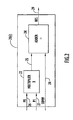
- the matrix multiplication hardware module 10 comprises a plurality of MAC units 20(1) to 20(N) and an array of dual port registers 30, referred to hereinafter as register array (RA) 30.
- register array (RA) 30 There are first and second memory banks 40 and 50 and first and second buses 60 and 70 that supply data to and from the module 10.
- Each memory bank 40 and 50 is dedicated to one of the two input matrices to be multiplied.
- the separate data buses 60 and 70 can be read simultaneously by the module 10. With this architecture, it is possible to read one data element from each input matrix at the same time.
- the output result can be saved in either memory bank.
- Memory bank 40 is connected to bus 60 and memory bank 50 is connected to bus 70.
- the module 10 comprises first and second input ports (In0 and In1) 80 and 90, respectively, and an output port (Out) 95.
- Bus 60 connects to the first input port 80 and the bus 70 connects to the second input port 90.
- the output port 95 of the matrix multiply module can be connected to either bus 60 or 70.
- the box shown at reference numeral 100 in FIG. 1 is provided to indicate that the components within the box 100 may be implemented in any programmable or fixed logic technology, such as a field programmable gate array (FPGA), application specific integrated circuit (ASIC), reconfigurable fixed logic circuits, programmable computing fabrics, etc.
- the data elements for the first and second matrices to be multiplied are received from the requesting device or software by configuration registers 110.
- the configuration registers 110 configure the matrix multiplication module 10 according to the dimensions of the first and second matrices.
- the MAC unit 20(i) comprises a multiplier circuit 22 and an adder circuit 24.
- An output 25 of the multiplier circuit is connected to one input of the adder circuit.
- a summation (SUMM) port 28 is connected to another input of the adder circuit 24.
- the SUMM port 28 receives an addend value from the result value generated by the adder circuit 24 and supplied to output 25 that was computed at a prior computation cycle.
- the input port 26 is connected to the first input 80 that in turn connects to the first bus 60 from which data elements of the first matrix are obtained.
- the input port 27 is connected to the second input 90 that in turn connects to the second bus 70 from which data elements of the second matrix are obtained.
- each MAC unit receives a data element of a first matrix and a data element of a second matrix.
- the SUMM port 28 is the third input port and in operation it receives data from another MAC unit.
- the output port 29 of the MAC unit 20(i) contains the result (RES) data that is the sum of the data on the SUMM port and the data on the output 25 of the multiplier 22.
- the RA 30 is a type of register array block that comprises an array (plurality) of registers that can be written to via one port and read from via another port.
- the RA 30 comprises "N" registers 32(0) to 32(N-1) addressed as "Register #0" to "Register #N-1".
- Each register cell comprises a number of bits equal to the number of bits needed to represent the data elements of the matrices to be multiplied.
- a register pointer (Register_Ptr) 33 is used to point to a particular register in the array to be read from or written to.
- Input data bus (Data_In) 34 is a bus used to write to any of the registers in the register array.
- Output data bus (Data_Out) 35 is a bus used to read from any of the registers in the register array.
- a write input signal (Write) 36 is used to signal the write operation of the input data to any of the registers in the register array.
- a read input signal (Read) 37 is used to signal the read operation of the output data from any of the registers in the register array.
- the RA 30 is a storage unit comprising a plurality of storage locations, each of which stores data elements from rows of the first matrix and from columns of the second matrix supplied to MAC units during one computation stage for use in a subsequent computation stage (actually in several subsequent computation stages).
- Any array of dual port storage locations may be used to serve the function of the RA 30, such as dual port block RAM, or dual port memory chips.
- the number of used MAC units depends on the size of the matrices to be multiplied.
- Two simple examples are provided to illustrate operation of the matrix multiplication module 10. The entire multiplication operation is performed while reading data from the two matrices to be multiplied. By the time all operand data is read, the product (result of multiplication of the two matrices) is ready. This assumes that there are two independent memory banks (as shown in FIG. 1 ) with each input matrix stored in a corresponding memory bank so that two elements, one from each matrix stored in the corresponding memory bank, can be read at the same time. Moreover, the number of computation stages associated with multiplying two matrices depends on, and is in fact, equal to the number of rows in the first matrix.
- data for a first matrix "m1" is stored in memory bank 40 and data for a second matrix “m2" is stored in memory bank 50.
- the result of the multiplication of matrix m1 x m2 is stored in matrix "m3" in memory bank 40.
- Data from matrix m1 is read one element at a time through input port 80.
- Data from matrix m2 is read one element at a time through input port 90.
- the matrix multiplication module 10 performs the matrix multiplication process while reading data from the two memory banks 40 and 50. By the time the matrix multiplication module finishes reading data elements of the two input matrices m1 and m2, the output result is ready at the output port 95 to be stored in memory bank 40 as matrix m3.
- bus width There are no restrictions regarding the bus width. The only limitation is the resources available on the logic technology selected to implement the module 10.
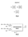
- each matrix in the computation matrix A and matrix B is a 2 x 2 matrix.
- the resultant matrix from the computation AxB is stored as matrix C.
- the two input matrices are stored in memory so that the first matrix of the two to be multiplied (that is, the matrix on the left side, matrix A in this example) is stored "row-wise" in memory bank 40, and the second matrix (matrix B in this example) is stored "column-wise” in memory bank 50.
- the data elements of the second matrix (matrix B) will be read out from memory sequentially in the following order: B ⁇ 1 ⁇ B ⁇ 2 ⁇ B ⁇ 3 ⁇ B ⁇ 4
- the input data flow for a 2x2 matrix multiplication operation is as follows.
- data elements A1 and B1 will be at the inputs input ports 80 and 90, respectively.
- data elements A2 and B2 will be at the inputs 80 and 90, respectively.
- data elements A3 and B3 will be at the inputs 80 and 90, respectively.
- data elements A4 and B4 will be at the inputs 80 and 90, respectively.
- the computation is divided into two computation stages for matrix A.
- the matrix multiplication module 10 uses a single MAC unit only.
- the matrix multiplication module uses three MAC units.
- FIGs. 6, 7A, 7B , 8 , 9A, 9B, 10A, 10B, 11A and 11B illustrate operation during the first and second clock cycles when a single MAC unit is used.
- the first and second clock cycles using a single MAC unit is the first computation stage.
- FIGs. 8 , 9A, 9B, 10A, 10B, 11A and 11B illustrate operation during the third and fourth clock cycles (that make up the second computation stage) when three MAC units are used.
- a maximum of three MAC units are used at any one time when multiplying two 2 x 2 matrices and the entire matrix multiplication computation lasts a time interval of four clock cycles and there are two computation stages, each of which comprises two clock cycles.
- data is applied to the inputs of the first MAC unit 20(1).
- the data elements A1 and B1 are read from memory (memory banks 40 and 50, respectively, as shown in FIG. 1 ) and applied to input ports 26 and 27, respectively, of a first MAC unit 20(1).
- data elements A1 and B1 are applied to respective storage locations of the RA 30 in order to produce the delayed versions A1 q and B1 q of input data elements A1 and B1, respectively, for use during the second computation stage.
- data elements A2 and B2 are read from memory and applied to input ports 26 and 27, respectively, of the MAC unit 20(1) and at the same time to respective storage locations of the RA 30 to produce delayed versions of data elements A2q and B2q, respectively, for use during the second computation stage.
- the input at the SUMM port 28 is taken as the result from the multiplication result A1*B1 at the end of the first clock cycle.
- the output at port 29 at the end of the first clock cycle is looped back to the SUMM input port 28 to be ready for the computation to take place during the second clock cycle.
- the data elements A2 and B2 are supplied to input ports 26 and 27, respectively, so that the multiplier circuit in the MAC unit 20(1) computes A2*B2 and the adder circuit in the MAC unit 20(1) adds that result to A1*B1 at the SUMM input port 28.
- the final result A1*B1 + A2*B2 is provided at the output port 29.
- FIGs. 8 , 9A, 9B, 10A, 10B, 11A and 11B operation during the second computation stage comprising the third and fourth clock cycles is described.
- Two more MAC units 20(2) and 20(3) are used during the third and fourth clock cycles.
- FIGs. 9A, 10A and 11A illustrate operation of the three MAC units 20(1), 20(2) and 20(3) during the third clock cycle
- FIGs. 9B, 10B and 11B illustrate operation of the three MAC units 20(1), 20(2) and 20(3) during the fourth clock cycle.
- Data elements A3 and B3 are read from memory and applied to inputs 26 and 27, respectively, of the first MAC unit 20(1), as shown at FIGs. 8 and 9A . As shown in FIGs.
- Data element A1 q is read from the RA 30 and applied to input 26 of the second MAC unit 20(2) and data element B3 is read from memory and applied to the input 27 of MAC unit 20(2).
- data element A3 is read from memory and applied to input 26 of the third MAC unit 20(3) and data element B1 q is read from the RA 30 and applied to input 27 of the third MAC unit 20(3), as shown in FIGs. 8 and 11A .
- MAC unit 20(1) computes A3*B3
- MAC unit 20(2) computes A1q*B3
- MAC unit 20(3) computes A3*B1q.
- data elements A4 and B4 are read from memory and applied to inputs 26 and 27, respectively, of MAC unit 20(1).
- the result A3*B3 computed by MAC unit 20(1) during the third clock cycle is looped back at the beginning of the fourth clock cycle to the SUMM input port of MAC unit 20(1).
- MAC unit 20(1) computes A4*B4 and adds that to A3*B3.
- the result output of MAC unit 20(1) at the end of the fourth clock cycle corresponds to the data element C4 of the result matrix C.
- data element A2q is read from the DPR 30 and applied to input 26 of MAC unit 20(2) and data element B4 is applied to input 27 of MAC unit 20(2).
- the result A1*B3 computed by MAC unit 20(2) during the third clock cycle is looped back at the beginning of the fourth clock cycle to the SUMM input port of MAC unit 20(2).
- MAC unit 20(2) computes A2*B4 and adds that value to A1*B3, and in so doing, outputs at its result output the data element C2 of the result matrix C.
- MAC unit 20(1) is used when reading data elements for the two rows of matrix A. Therefore, MAC 20(1) is used for four clock cycles, MAC 20(2) is used for two clock cycles, and MAC 20(3) is used for two clock cycles.
- the SUMM input port to each MAC unit is reset to zero at the beginning of each computation stage (corresponding to a new row of data elements) read from the first matrix, matrix A.
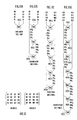
- FIG. 12 illustrates two 4x4 matrices.
- FIGs. 13A, 13B, 13C and 13D show the details of the multiplication operations for multiplying matrices A and B shown in FIG. 12 .
- the operation takes 16 clock cycles and uses no more than seven MAC units.
- FIG. 13A is the first computation stage
- FIG. 13B is the second computation stage
- FIG. 13C is the third computation stage
- FIG. 13D is the fourth computation stage.
- Each of the computation stages shown in FIGs. 13A-13D lasts four clock cycles as indicated by the stack of four data elements about each MAC unit.
- FIG. 13A shows that one MAC unit is used when reading the first row of matrix A as shown in FIG. 13A .
- Two additional MAC units are used when reading the second row of matrix A, making a total of three MAC units, as shown in FIGs. 13B.
- FIG. 13C shows that two more MAC units are used when reading from the third row of matrix A, making for a total of five MAC units.
- FIG. 13D shows that seven MAC units are used as shown in FIG. 13D .
- 12 and 13A-13D performs the "loop back" operation from its output to its SUMM input even though this is not shown in FIGs. 13A-13D .
- MAC unit 20(1) adds A1*B1 computed during the first clock cycle and looped back to the SUMM input of MAC unit 20(1) (though not shown in FIG. 13A ), to A2*B2 computed during the second clock cycle. Further, the summation A1*B1 + A2*B2 is looped back to the SUMM input of the MAC unit 20(1) such that during the third clock cycle, MAC unit 20(1) computes A3*B3 and adds that product value to A1*B1 + A2*B2.
- the MAC unit 20(1) computes A4*B4 and adds that product value to A1*B1 + A2*B2 + A3*B3 looped back to the SUMM input of MAC unit 20(1) at the end of the third clock cycle.
- the first element, C1 of the resulting matrix C for multiplication of the matrices shown in FIG. 12 is computed by MAC unit 20(1) in four clock cycles.
- a similar loop back summation function is performed by each of the MAC units in the second, third and fourth computation stages represented by FIGs. 13B, 13C and 13D , respectively.
- data elements for the A and B matrices that are read from memory and supplied to a MAC unit during one computation stage are written to the RA for use during subsequent computation stages in much the same way as described above in the 2 x 2 matrix computation example.
- a single MAC unit is used to multiply data elements of the first row of the first matrix with data elements of a first column of the second matrix.
- the first row of a matrix need not be the top row of the matrix and the first column of a matrix need not be the leftmost row of a matrix.
- the total (maximum) number of MAC units depends on the total number of rows of the left side matrix. To multiply an NxM matrix by an MxN matrix, the total (maximum) number of used MAC units is "2*N-1".
- the number of MAC units used starts with one (1) during the first computation stage (first row of left matrix), and increases by two units at each subsequent computation stage (each subsequent row of the left matrix).
- the sequence of the number of MAC units is ⁇ 1, 3, 5, ..., 2*N-1 ⁇ for the computation stages, where, again, each computation stage corresponds to reading of data elements for each new row of the left side matrix, also called the first matrix.
- the matrix multiplication module 10 operates such that during the jth computation stage corresponding to the jth row of the first matrix, the number of multiplier-accumulator units used is limited to the amount necessary in order to (i) multiply data elements for the jth row of the first matrix by data elements for the jth column and by data elements for all preceding columns of the second matrix and (ii) to multiply data elements for all rows of the first matrix preceding the jth row by data elements for the jth column of the second matrix. Moreover, during the jth computation stage, data elements for the jth row of the first matrix and for all preceding rows are stored in respective storage locations of the storage unit for use in computation stages after the jth computation stage.
- each MAC unit that is used is operated for a plurality of clock cycles equal in number to a number of rows of the first matrix.
- the adder circuit in each MAC unit adds the product value computed by the multiplier circuit at the current clock cycle with the result value computed by the adder circuit at a previous clock cycle for that computation stage. If it is the beginning (first clock cycle) of a computation stage, then the SUMM input to each MAC unit is reset to 0.
- the matrix multiplication module 10 is scalable and can be adapted for use on larger matrices.
- the module 10 may be used to multiply 16x16 or 32x32 matrices if the module 10 is implemented in a relatively large FPGA.
- the matrix multiplication module 10 was built with a Xilinx Vertix2 FPGA (in a 3 million-gate FPGA chip form factor). For a multiplication of two 8 x 8 matrices, peak performance of 16 floating point operations per clock cycle was achieved. Running the FPGA at 100 MHz a peak performance of 1.6 giga-floating point operations per second (GFLOPS/sec) can be obtained.
- GFLOPS/sec giga-floating point operations per second
- multiplying 16x16 or 32x32 matrices can be performed with a peak performance of 32 and 64 GFLOPS/sec, respectively, at a speed of 100 MHz.
- the performance is equal to 2*N floating point operations per clock, where N is the number of rows of the first (left hand side) matrix regardless on the number of its columns.
- the matrix multiplication examples described herein involve square matrices. However, the same concept can be applied for non-square matrices. The performance is based on the number of rows of the left hand matrix. Therefore, the same concept can be applied to left hand matrices with number of rows equals 16 or 32 to give performance of 3.2 or 6.4 GFLOPS/sec respectively running at 100 MHz clock. Performance increases with the use of faster clock frequencies.
- the matrix multiplication module described above may be used to multiply non-square matrices. Multiplying a 4xN matrix and an Nx4 matrix is similar to the example of multiplying two 4x4 matrices. The only difference is that N clock cycles are needed to read the rows of the first (left hand side) matrix. Nevertheless, the performance is the same as that described above: 8 floating point operations per clock cycle if the first matrix has 4 rows, and 16 floating point operations per clock cycle if the first matrix has 8 rows.
- the resources of an FPGA chip may not be enough to process the multiplication process in one block.
- the matrices may be partitioned into smaller blocks such that each block can fit within the resources of the FPGA.
- the matrix multiplication operation is performed on a block-by-block basis, and then the results of the multiplication of the individual blocks are combined to form the resultant matrix.
- the matrix multiplication module 10 may be employed to multiply two matrices using a variety of data types, such as 32-bit single precision floating point data and 64-bit double precision floating point data. Moreover, the module 10 may operate using 32-bit or 64-bit integer or fixed floating point data based on the width of the used memory banks. Further still, any non-standard data type may be used.
- the register array of the RA 30 needs to be deep enough to store at least two rows of data elements (one row from each input matrix) when buffering data elements for use during subsequent clock cycles as explained in the foregoing. Otherwise, the size of the register array is left to the designer.
Abstract
Description
- The present invention relates to matrix multiplication device, hardware module or core, and more particularly to the use of a variable number of multiplier-accumulators based on the data elements to be multiplied during stages of a matrix multiplication operation.
- Matrix multiplication is a necessary computation operation in many scientific and engineering applications. For example, navigation and control applications often require multiplication of matrices, sometimes very large matrices. Researchers have looked for solutions to enhance the performance of the matrix multiplication.
- Matrix multiplication requires significant computation resources. To multiply two N x N matrices, N * N * N multiplication operations and (N-1) * N * N addition operations are needed. All matrix multiplication solutions depend upon either distributed data or distributed operations. However, all matrix multiplication solutions heretofore known are based on the assumption that there are a fixed number of available multipliers and accumulators.
- Certain applications of matrix multiplication operations require highly efficient uses of resources in order to produce the result quickly using minimal computation and resources and consuming as little power as possible. Examples of such applications are in space vehicles and other equipment that carry finite power supplies.
- Briefly, a matrix multiplication module and matrix multiplication method are provided that use a variable number of multiplier-accumulator units based on the amount of data elements of the matrices are available or needed for processing at a particular point or stage in the computation process. As more data elements become available or are needed, more multiplier-accumulator units are used to perform the necessary multiplication and addition operations.
- Accordingly, a matrix multiplication module or hardware device is provided comprising a plurality of multiplier-accumulator units each of which comprises a multiplier circuit that multiplies two data elements to produce a product value and an adder circuit that adds the product value with an addend value to produce a result value. The number of multiplier-accumulator units used when a multiplication computation is performed on first and second matrices varies depending on which computation stage corresponding to which row of the first matrix the multiplication computation is executing.
- Similarly, a method for multiplying first and second matrices is provided comprising providing a plurality of multiplier-accumulator units, each of which is capable of multiplying one data element of the first matrix with a data element of the second matrix to produce a product value and adding the product value with an addend value to produce a result value; and using a number of said plurality of multiplier-accumulator units that increases as computation progresses from a first row of the first matrix to remaining rows of the first matrix.
-
- FIG. 1
- is a block diagram of a matrix multiplication hardware module according to an embodiment of the invention.
- FIG. 2
- is a block diagram of a multiplier-accumulator unit used in the matrix multiplication hardware module according to embodiments of the present invention.
- FIG. 3
- is a block diagram of a dual port register array forming a part of the matrix multiplication hardware module according to an embodiment of the invention.
- FIG. 4
- is a diagram illustrating elements of two 2x2 matrices to be multiplied by the matrix multiplication module according to the invention.
- FIG. 5
- illustrates input data flow for the multiplication of the two matrices shown in
FIG. 4 , according to an embodiment of the invention. - FIG. 6
- illustrates operation of a first multiplier-accumulator unit in the matrix multiplication example shown in
FIGs. 4 and 5 . - FIG. 7A
- is a diagram illustrating computations made by the first multiplier- accumulator during a first clock cycle depicted in
FIG. 6 . - FIG. 7B
- is a diagram illustrating computations made by the first multiplier- accumulator during a second clock cycle depicted in
FIG. 6 . - FIG. 8
- illustrates operation of three multiplier-accumulator units in the matrix multiplication example shown in
FIGs. 4 and 5 . - FIGs. 9A and 9B
- illustrate operation of a first multiplier-accumulator unit during successively clock cycles in the matrix multiplication example shown in
FIGs. 4 and 5 . - FIGs. 10A and 10B
- illustrate operation of a second multiplier-accumulator unit during successively clock cycles in the matrix multiplication example shown in
FIGs. 4 and 5 . - FIGs. 11A and 11 B
- illustrate operation of a third multiplier-accumulator unit during successively clock cycles in the matrix multiplication example shown in
FIGs. 4 and 5 . - FIG. 12
- illustrates an example of two 4x4 matrices to be multiplied by the matrix multiplication module according to an embodiment of the invention.
- FIG. 13A
- illustrates operation of a first multiplier-accumulator unit during a first computation stage of the matrix multiplication example shown in
FIG. 12 . - FIG. 13B
- illustrates operation of three multiplier-accumulator units during a second computation stage of the matrix multiplication example shown in
FIG. 12 . - FIG. 13C
- illustrates operation of five multiplier-accumulator units during a third computation stage of the matrix multiplication example shown in
FIG. 12 . - FIG. 13D
- illustrates operation of seven multiplier-accumulator units during a fourth computation stage of the matrix multiplication example shown in
FIG. 12 . - According to the present invention, a matrix multiplication hardware module (also called a "core") is provided that uses a variable number of multiplier-accumulator (MAC) units based on the number of data elements available for processing. The number of MAC units used during a multiplication of two matrices varies over time depending on the stage of the computation of the matrices. In one embodiment, the number of MAC units increases over time during a computation of two matrices.
- The total (maximum) number of used MAC units is based on the size of the matrices to be multiplied. For specific sizes of the matrices, the number of used MAC units increases according to the availability of data during a computation session of two matrices. For example, when reading the first element from each matrix, only one MAC unit is needed to perform the multiply/add operation. The more data that is read as the computation progresses through the matrices, the more MAC units are used to perform multiply/add operations. Thus, in one embodiment, the matrix multiplication module has a dynamically increasing number of MAC units.
- Referring first to
FIG. 1 , the matrix multiplication hardware module is shown atreference numeral 10. The matrixmultiplication hardware module 10 comprises a plurality of MAC units 20(1) to 20(N) and an array of dual port registers 30, referred to hereinafter as register array (RA) 30. There are first andsecond memory banks second buses module 10. Eachmemory bank separate data buses module 10. With this architecture, it is possible to read one data element from each input matrix at the same time. The output result can be saved in either memory bank.Memory bank 40 is connected tobus 60 andmemory bank 50 is connected tobus 70. Themodule 10 comprises first and second input ports (In0 and In1) 80 and 90, respectively, and an output port (Out) 95.Bus 60 connects to thefirst input port 80 and thebus 70 connects to thesecond input port 90. Theoutput port 95 of the matrix multiply module can be connected to eitherbus - The box shown at
reference numeral 100 inFIG. 1 is provided to indicate that the components within thebox 100 may be implemented in any programmable or fixed logic technology, such as a field programmable gate array (FPGA), application specific integrated circuit (ASIC), reconfigurable fixed logic circuits, programmable computing fabrics, etc. The data elements for the first and second matrices to be multiplied are received from the requesting device or software by configuration registers 110. The configuration registers 110 configure thematrix multiplication module 10 according to the dimensions of the first and second matrices. - Turning to
FIG. 2 , the ports of a MAC unit 20(i) are described. The MAC unit 20(i) comprises amultiplier circuit 22 and anadder circuit 24. Anoutput 25 of the multiplier circuit is connected to one input of the adder circuit. A summation (SUMM)port 28 is connected to another input of theadder circuit 24. As described hereinafter, theSUMM port 28 receives an addend value from the result value generated by theadder circuit 24 and supplied tooutput 25 that was computed at a prior computation cycle. There are two input ports (P0 and P1) 26 and 27, respectively, that supply the two data elements to the MAC unit 20(i) to be multiplied. Theinput port 26 is connected to thefirst input 80 that in turn connects to thefirst bus 60 from which data elements of the first matrix are obtained. Similarly, theinput port 27 is connected to thesecond input 90 that in turn connects to thesecond bus 70 from which data elements of the second matrix are obtained. Thus, when two matrices are being multiplied, each MAC unit receives a data element of a first matrix and a data element of a second matrix. TheSUMM port 28 is the third input port and in operation it receives data from another MAC unit. Theoutput port 29 of the MAC unit 20(i) contains the result (RES) data that is the sum of the data on the SUMM port and the data on theoutput 25 of themultiplier 22. - Reference is now made to
FIG. 3 where the register array (RA) 30 is shown in more detail. TheRA 30 is a type of register array block that comprises an array (plurality) of registers that can be written to via one port and read from via another port. TheRA 30 comprises "N" registers 32(0) to 32(N-1) addressed as "Register # 0" to "Register #N-1". Each register cell comprises a number of bits equal to the number of bits needed to represent the data elements of the matrices to be multiplied. - A register pointer (Register_Ptr) 33 is used to point to a particular register in the array to be read from or written to. Input data bus (Data_In) 34 is a bus used to write to any of the registers in the register array. Output data bus (Data_Out) 35 is a bus used to read from any of the registers in the register array. A write input signal (Write) 36 is used to signal the write operation of the input data to any of the registers in the register array. A read input signal (Read) 37 is used to signal the read operation of the output data from any of the registers in the register array.
- Thus, the
RA 30 is a storage unit comprising a plurality of storage locations, each of which stores data elements from rows of the first matrix and from columns of the second matrix supplied to MAC units during one computation stage for use in a subsequent computation stage (actually in several subsequent computation stages). Any array of dual port storage locations may be used to serve the function of theRA 30, such as dual port block RAM, or dual port memory chips. - As indicated above, the number of used MAC units depends on the size of the matrices to be multiplied. Two simple examples are provided to illustrate operation of the
matrix multiplication module 10. The entire multiplication operation is performed while reading data from the two matrices to be multiplied. By the time all operand data is read, the product (result of multiplication of the two matrices) is ready. This assumes that there are two independent memory banks (as shown inFIG. 1 ) with each input matrix stored in a corresponding memory bank so that two elements, one from each matrix stored in the corresponding memory bank, can be read at the same time. Moreover, the number of computation stages associated with multiplying two matrices depends on, and is in fact, equal to the number of rows in the first matrix. - For example, data for a first matrix "m1" is stored in
memory bank 40 and data for a second matrix "m2" is stored inmemory bank 50. The result of the multiplication of matrix m1 x m2 is stored in matrix "m3" inmemory bank 40. Data from matrix m1 is read one element at a time throughinput port 80. Data from matrix m2 is read one element at a time throughinput port 90. Thematrix multiplication module 10 performs the matrix multiplication process while reading data from the twomemory banks output port 95 to be stored inmemory bank 40 as matrix m3. - There are no restrictions regarding the bus width. The only limitation is the resources available on the logic technology selected to implement the
module 10. - Operation of the
matrix multiplication module 10 is now described in more detail with reference toFIGs. 4-7 . As shown inFIG. 4 , in this example, each matrix in the computation matrix A and matrix B is a 2 x 2 matrix. The resultant matrix from the computation AxB is stored as matrix C. - The elements of the result matrix should be:


- In the
matrix multiplication module 10, the two input matrices are stored in memory so that the first matrix of the two to be multiplied (that is, the matrix on the left side, matrix A in this example) is stored "row-wise" inmemory bank 40, and the second matrix (matrix B in this example) is stored "column-wise" inmemory bank 50. As shown inFIG. 5 , this means the data elements of the first matrix (matrix A) will be read out from memory sequentially in the following order:
- The data elements of the second matrix (matrix B) will be read out from memory sequentially in the following order:

- More specifically, as shown in
FIG. 5 , the input data flow for a 2x2 matrix multiplication operation is as follows. At the first clock cycle, data elements A1 and B1 will be at theinputs input ports inputs inputs inputs - In the case of 2x2 matrix multiplication, the computation is divided into two computation stages for matrix A. During a first computation stage when the first row of matrix A is being read, the
matrix multiplication module 10 uses a single MAC unit only. During a second computation stage when the second row of matrix A is being read, the matrix multiplication module uses three MAC units. - Reference is now made to
FIGs. 6, 7A, 7B ,8 ,9A, 9B, 10A, 10B, 11A and 11B for a more detailed explanation of the operation of the matrix multiplication module on a per-clock cycle basis.FIGs. 6, 7A and 7B illustrate operation during the first and second clock cycles when a single MAC unit is used. In this example, the first and second clock cycles using a single MAC unit is the first computation stage.FIGs. 8 ,9A, 9B, 10A, 10B, 11A and 11B illustrate operation during the third and fourth clock cycles (that make up the second computation stage) when three MAC units are used. Thus, a maximum of three MAC units are used at any one time when multiplying two 2 x 2 matrices and the entire matrix multiplication computation lasts a time interval of four clock cycles and there are two computation stages, each of which comprises two clock cycles. - During the first two clock cycles, data is applied to the inputs of the first MAC unit 20(1). Specifically, as shown in
FIG. 7A with continued reference toFIG. 6 , during the first clock cycle, the data elements A1 and B1 are read from memory (memory banks FIG. 1 ) and applied to inputports RA 30 in order to produce the delayed versions A1 q and B1 q of input data elements A1 and B1, respectively, for use during the second computation stage. - As shown in
FIG. 7B with continued reference toFIG. 6 , during the second clock cycle, data elements A2 and B2 are read from memory and applied to inputports RA 30 to produce delayed versions of data elements A2q and B2q, respectively, for use during the second computation stage. During the second clock cycle, the input at theSUMM port 28 is taken as the result from the multiplication result A1*B1 at the end of the first clock cycle. Thus, the output atport 29 at the end of the first clock cycle is looped back to theSUMM input port 28 to be ready for the computation to take place during the second clock cycle. The data elements A2 and B2 are supplied to inputports SUMM input port 28. The final result A1*B1 + A2*B2 is provided at theoutput port 29. - Thus, the output of the first MAC unit 20(1) after the second clock signal is the C1 data element of the result matrix C. It should be understood that A1 = A1q, A2 = A2q, B1 = B1q and B2 = B2q.
- Turning to
FIGs. 8 ,9A, 9B, 10A, 10B, 11A and 11B , operation during the second computation stage comprising the third and fourth clock cycles is described. Two more MAC units 20(2) and 20(3) are used during the third and fourth clock cycles.FIGs. 9A, 10A and 11A illustrate operation of the three MAC units 20(1), 20(2) and 20(3) during the third clock cycle, andFIGs. 9B, 10B and 11B illustrate operation of the three MAC units 20(1), 20(2) and 20(3) during the fourth clock cycle. Data elements A3 and B3 are read from memory and applied toinputs FIGs. 8 and9A . As shown inFIGs. 8 and10A , Data element A1 q is read from theRA 30 and applied to input 26 of the second MAC unit 20(2) and data element B3 is read from memory and applied to theinput 27 of MAC unit 20(2). Finally, during the third clock cycle, data element A3 is read from memory and applied to input 26 of the third MAC unit 20(3) and data element B1 q is read from theRA 30 and applied to input 27 of the third MAC unit 20(3), as shown inFIGs. 8 and11A . Thus, during the third clock cycle, MAC unit 20(1) computes A3*B3, MAC unit 20(2) computes A1q*B3, and MAC unit 20(3) computes A3*B1q. - With reference to
FIGs. 8 and9B , during the fourth clock cycle, data elements A4 and B4 are read from memory and applied toinputs - With reference to
FIGs. 8 and10B , during the fourth clock cycle, data element A2q is read from theDPR 30 and applied to input 26 of MAC unit 20(2) and data element B4 is applied to input 27 of MAC unit 20(2). The result A1*B3 computed by MAC unit 20(2) during the third clock cycle is looped back at the beginning of the fourth clock cycle to the SUMM input port of MAC unit 20(2). Thus, during the fourth clock cycle MAC unit 20(2) computes A2*B4 and adds that value to A1*B3, and in so doing, outputs at its result output the data element C2 of the result matrix C. - Finally, with reference to
FIGs. 8 and11B , during the fourth clock cycle, data element A3 is applied to input 26 of the third MAC unit 20(3) and data element B2q is read from theRA 30 and applied to theinput 27 of MAC unit 20(3). The result A3*B1 computed by MAC unit 20(3) during the third clock cycle is looped back at the beginning of the fourth clock cycle to the SUMM input port of MAC unit 20(3). Consequently, during the fourth clock cycle, MAC unit 20(3) computes A4*B2 and adds the result with A3*B1 to produce at its output the data element C3 for the result matrix C. - Noteworthy from
FIGs. 6, 7A and 7B is that the same MAC unit, MAC unit 20(1), is used when reading data elements for the two rows of matrix A. Therefore, MAC 20(1) is used for four clock cycles, MAC 20(2) is used for two clock cycles, and MAC 20(3) is used for two clock cycles. The SUMM input port to each MAC unit is reset to zero at the beginning of each computation stage (corresponding to a new row of data elements) read from the first matrix, matrix A. - The same concept is applied to the example of multiplying two 4x4 matrices.
FIG. 12 illustrates two 4x4 matrices.FIGs. 13A, 13B, 13C and 13D show the details of the multiplication operations for multiplying matrices A and B shown inFIG. 12 . The operation takes 16 clock cycles and uses no more than seven MAC units.FIG. 13A is the first computation stage,FIG. 13B is the second computation stage,FIG. 13C is the third computation stage andFIG. 13D is the fourth computation stage. Each of the computation stages shown inFIGs. 13A-13D lasts four clock cycles as indicated by the stack of four data elements about each MAC unit. - During the operation, one MAC unit is used when reading the first row of matrix A as shown in
FIG. 13A . Two additional MAC units are used when reading the second row of matrix A, making a total of three MAC units, as shown inFIGs. 13B. FIG. 13C shows that two more MAC units are used when reading from the third row of matrix A, making for a total of five MAC units. Finally, when reading from the fourth row of matrix A, a total of seven MAC units are used as shown inFIG. 13D . It should be understood from the 2 x 2 matrix multiplication example described above that each MAC unit shown in the 4 x 4 matrix multiplication example ofFIGs. 12 and 13A-13D performs the "loop back" operation from its output to its SUMM input even though this is not shown inFIGs. 13A-13D . For example, during the first computation stage, at the second clock cycle, MAC unit 20(1) adds A1*B1 computed during the first clock cycle and looped back to the SUMM input of MAC unit 20(1) (though not shown inFIG. 13A ), to A2*B2 computed during the second clock cycle. Further, the summation A1*B1 + A2*B2 is looped back to the SUMM input of the MAC unit 20(1) such that during the third clock cycle, MAC unit 20(1) computes A3*B3 and adds that product value to A1*B1 + A2*B2. Finally, during the fourth clock cycle of the first computation stage shown inFIG. 13A , the MAC unit 20(1) computes A4*B4 and adds that product value to A1*B1 + A2*B2 + A3*B3 looped back to the SUMM input of MAC unit 20(1) at the end of the third clock cycle. Thus, the first element, C1, of the resulting matrix C for multiplication of the matrices shown inFIG. 12 , is computed by MAC unit 20(1) in four clock cycles. A similar loop back summation function is performed by each of the MAC units in the second, third and fourth computation stages represented byFIGs. 13B, 13C and 13D , respectively. In addition, data elements for the A and B matrices that are read from memory and supplied to a MAC unit during one computation stage are written to the RA for use during subsequent computation stages in much the same way as described above in the 2 x 2 matrix computation example. - During a first computation corresponding to a first row of the first matrix, a single MAC unit is used to multiply data elements of the first row of the first matrix with data elements of a first column of the second matrix. It should be understood that the first row of a matrix need not be the top row of the matrix and the first column of a matrix need not be the leftmost row of a matrix. In general, the total (maximum) number of MAC units depends on the total number of rows of the left side matrix. To multiply an NxM matrix by an MxN matrix, the total (maximum) number of used MAC units is "2*N-1". The number of MAC units used starts with one (1) during the first computation stage (first row of left matrix), and increases by two units at each subsequent computation stage (each subsequent row of the left matrix). The sequence of the number of MAC units is {1, 3, 5, ..., 2*N-1} for the computation stages, where, again, each computation stage corresponds to reading of data elements for each new row of the left side matrix, also called the first matrix. The
matrix multiplication module 10 operates such that during the jth computation stage corresponding to the jth row of the first matrix, the number of multiplier-accumulator units used is limited to the amount necessary in order to (i) multiply data elements for the jth row of the first matrix by data elements for the jth column and by data elements for all preceding columns of the second matrix and (ii) to multiply data elements for all rows of the first matrix preceding the jth row by data elements for the jth column of the second matrix. Moreover, during the jth computation stage, data elements for the jth row of the first matrix and for all preceding rows are stored in respective storage locations of the storage unit for use in computation stages after the jth computation stage. Further still, during each computation stage, each MAC unit that is used is operated for a plurality of clock cycles equal in number to a number of rows of the first matrix. The adder circuit in each MAC unit adds the product value computed by the multiplier circuit at the current clock cycle with the result value computed by the adder circuit at a previous clock cycle for that computation stage. If it is the beginning (first clock cycle) of a computation stage, then the SUMM input to each MAC unit is reset to 0. - The
matrix multiplication module 10 is scalable and can be adapted for use on larger matrices. For example, themodule 10 may be used to multiply 16x16 or 32x32 matrices if themodule 10 is implemented in a relatively large FPGA. Thematrix multiplication module 10 was built with a Xilinx Vertix2 FPGA (in a 3 million-gate FPGA chip form factor). For a multiplication of two 8 x 8 matrices, peak performance of 16 floating point operations per clock cycle was achieved. Running the FPGA at 100 MHz a peak performance of 1.6 giga-floating point operations per second (GFLOPS/sec) can be obtained. Thus, multiplying 16x16 or 32x32 matrices can be performed with a peak performance of 32 and 64 GFLOPS/sec, respectively, at a speed of 100 MHz. In general, the performance is equal to 2*N floating point operations per clock, where N is the number of rows of the first (left hand side) matrix regardless on the number of its columns. - The matrix multiplication examples described herein involve square matrices. However, the same concept can be applied for non-square matrices. The performance is based on the number of rows of the left hand matrix. Therefore, the same concept can be applied to left hand matrices with number of rows equals 16 or 32 to give performance of 3.2 or 6.4 GFLOPS/sec respectively running at 100 MHz clock. Performance increases with the use of faster clock frequencies.
- The matrix multiplication module described above may be used to multiply non-square matrices. Multiplying a 4xN matrix and an Nx4 matrix is similar to the example of multiplying two 4x4 matrices. The only difference is that N clock cycles are needed to read the rows of the first (left hand side) matrix. Nevertheless, the performance is the same as that described above: 8 floating point operations per clock cycle if the first matrix has 4 rows, and 16 floating point operations per clock cycle if the first matrix has 8 rows.
- In the case of very large matrices, the resources of an FPGA chip may not be enough to process the multiplication process in one block. In this case, the matrices may be partitioned into smaller blocks such that each block can fit within the resources of the FPGA. The matrix multiplication operation is performed on a block-by-block basis, and then the results of the multiplication of the individual blocks are combined to form the resultant matrix.
- However, the
matrix multiplication module 10 may be employed to multiply two matrices using a variety of data types, such as 32-bit single precision floating point data and 64-bit double precision floating point data. Moreover, themodule 10 may operate using 32-bit or 64-bit integer or fixed floating point data based on the width of the used memory banks. Further still, any non-standard data type may be used. - The register array of the
RA 30 needs to be deep enough to store at least two rows of data elements (one row from each input matrix) when buffering data elements for use during subsequent clock cycles as explained in the foregoing. Otherwise, the size of the register array is left to the designer. - The system and methods described herein may be embodied in other specific forms without departing from the spirit or essential characteristics thereof. The foregoing embodiments are therefore to be considered in all respects illustrative and not meant to be limiting.
Claims (18)
- A matrix multiplication device (10) , comprising a plurality of multiplier-accumulator units (20) each of which comprises a multiplier circuit (22) that multiplies two data elements to produce a product value and an adder (24) circuit that adds the product value with an addend value to produce a result value, wherein a number of multiplier-accumulator units (20) used when a multiplication computation is performed on first and second matrices varies depending on which computation stage corresponding to which row of the first matrix the multiplication computation is executing.
- The device (10) of claim 1, and further comprising a storage unit (30) comprising a plurality of storage locations, wherein the storage unit stores data elements of the first and second matrices that are applied to a multiplier-accumulator unit during a computation stage for use in a subsequent computation stage.
- A matrix multiplication hardware core (10) that multiplies first and second matrices, comprising:(a) a plurality of multiplier-accumulator units (20) each of which multiplies (22) a first data element from the first matrix with a second data element from the second matrix to produce a product value and adds (24) the product value with an addend value to produce a result value, wherein a number of multiplier-accumulator units used when multiplying the first and second matrices increases as computations progress from a first row of the first matrix to remaining rows of the first matrix; and(b) a storage unit (30) comprising a plurality of registers that store data elements for one or more rows of the first matrix and for one or more columns of the second matrix for subsequent supply as input to a multiplier-accumulator unit.
- The device of claim 2 or 3, and further comprising first and second memories (40, 50) , the first memory storing data elements of the first matrix and the second memory storing data elements of the second matrix.
- The device of claim 4, and further comprising a first input port and a second input port (80) , a first bus (60) that couples data between the first memory (40) and the first input port and a second bus (70) that couples data between the second memory (50) and the second input port (90).
- The device of one of claims 1 to 5, wherein each multiplier-accumulator unit (20) comprises a first input (26) that receives a data element of the first matrix and a second input (27) that receives a data element of the second matrix.
- The device of one of claims 1 to 6, during the jth computation stage corresponding to the jth row of the first matrix, the number of multiplier-accumulator units used is sufficient in order to multiply data elements for the jth row of the first matrix by data elements for the jth column of the second matrix and all preceding columns of the second matrix, and to multiply data elements for all rows of the first matrix preceding the jth row by data elements for the jth column of the second matrix.
- The device of one of claims 1 to 6, wherein during the jth computation stage, data elements for the jth row of the first matrix and for all preceding rows are stored in respective storage locations of the storage unit for use in computation stages after the jth computation stage.
- The device of one of claims 1 to 8, wherein during each computation stage, each multiplier-accumulator unit (20) that is used is operated for a plurality of clock cycles equal in number to a number of rows of the first matrix.
- The device of one of claims 1 to 9, wherein the adder circuit (24) in each multiplier-accumulator unit (20) adds the product value computed by the multiplier circuit at a current clock cycle with the result value computed by the adder circuit at a previous clock cycle for that computation stage.
- The device of one of claims 1 to 10, wherein during a first computation stage corresponding to a first row of the first matrix, a single multiplier-accumulator unit (20) is used to multiply data elements of the first row of the first matrix with data elements of the first column of the second matrix.
- The device of one of claims 1 to 11, wherein when multiplying a first matrix comprising NxM data elements by a second matrix comprising MxN data elements, the number of multiplier-accumulator units used during a sequence of computation stages is {1, 3, 5, ..., 2*N-1}.
- A method for multiplying first and second matrices, comprising:(a) providing a plurality of multiplier-accumulator units (20) , each of which is capable of multiplying one data element of the first matrix with a data element of the second matrix to produce a product value and adding the product value with an addend value to produce a result value; and(b) using a number of said plurality of multiplier-accumulator units that increases as computation progresses from a first row of the first matrix to remaining rows of the first matrix.
- The method of claim 13, wherein (b) using comprises, during a jth computation stage corresponding to a jth row of the first matrix, using a number of multiplier-accumulator units that is sufficient in order to multiply data elements for the jth row of the first matrix by data elements for the jth column of the second matrix and all preceding columns of the second matrix, and to multiply data elements for all rows of the first matrix preceding the jth row by data elements for the jth column of the second matrix.
- The method of claim 14, and further comprising, during the jth computation stage, storing data elements for the jth row of the first matrix and for all preceding rows in respective storage locations for use in computation stages after the jth computation stage.
- The method of one of claims 13 to 15, and further comprising during each computation stage, operating each multiplier-accumulator unit for a plurality of clock cycles equal in number to the number of rows of the first matrix.
- The method of one of claims 13 to 16, and further comprising adding a product value computed by a multiplier-accumulator unit at a current clock cycle with the result value computed by the result computed by the multiplier-accumulator circuit at the previous clock cycle.
- The method of one of claims 13 to 17, wherein when the first matrix comprises NxM data elements and the second matrix comprises MxN data elements, using comprises using the number of multiplier-accumulator units during a sequence of computation stages according to a sequence {1, 3, 5, ..., 2*N-1}.
Applications Claiming Priority (1)
| Application Number | Priority Date | Filing Date | Title |
|---|---|---|---|
| US11/779,935 US8051124B2 (en) | 2007-07-19 | 2007-07-19 | High speed and efficient matrix multiplication hardware module |
Publications (3)
| Publication Number | Publication Date |
|---|---|
| EP2017743A2 true EP2017743A2 (en) | 2009-01-21 |
| EP2017743A3 EP2017743A3 (en) | 2009-07-22 |
| EP2017743B1 EP2017743B1 (en) | 2012-12-12 |
Family
ID=39929976
Family Applications (1)
| Application Number | Title | Priority Date | Filing Date |
|---|---|---|---|
| EP08159750A Not-in-force EP2017743B1 (en) | 2007-07-19 | 2008-07-04 | High speed and efficient matrix multiplication hardware module |
Country Status (4)
| Country | Link |
|---|---|
| US (1) | US8051124B2 (en) |
| EP (1) | EP2017743B1 (en) |
| JP (1) | JP5408913B2 (en) |
| AU (1) | AU2008202591B2 (en) |
Cited By (7)
| Publication number | Priority date | Publication date | Assignee | Title |
|---|---|---|---|---|
| CN102411558A (en) * | 2011-10-31 | 2012-04-11 | 中国人民解放军国防科学技术大学 | Vector processor oriented large matrix multiplied vectorization realizing method |
| CN102629189A (en) * | 2012-03-15 | 2012-08-08 | 湖南大学 | Water floating point multiply-accumulate method based on FPGA |
| CN103135960A (en) * | 2013-02-28 | 2013-06-05 | 浪潮集团有限公司 | Design method of integrated floating point unit based on FPGA (field programmable gate array) |
| CN105893333A (en) * | 2016-03-25 | 2016-08-24 | 合肥工业大学 | Hardware circuit for calculating covariance matrix in MUSIC algorithm |
| WO2018228703A1 (en) * | 2017-06-16 | 2018-12-20 | Huawei Technologies Co., Ltd. | Multiply accumulator array and processor device |
| CN109992742A (en) * | 2017-12-29 | 2019-07-09 | 华为技术有限公司 | A kind of signal processing method and device |
| CN111316261A (en) * | 2017-11-01 | 2020-06-19 | 苹果公司 | Matrix calculation engine |
Families Citing this family (39)
| Publication number | Priority date | Publication date | Assignee | Title |
|---|---|---|---|---|
| CN101577025B (en) * | 2009-06-15 | 2011-11-23 | 上海华魏光纤传感技术有限公司 | Novel data acquisition accumulator and implementation method thereof |
| TW201232476A (en) * | 2011-01-27 | 2012-08-01 | Univ Nat Taiwan | Detection system and signal processing method thereof |
| CN104662531A (en) * | 2012-04-23 | 2015-05-27 | 惠普发展公司,有限责任合伙企业 | Statistical analysis using graphics processing unit |
| US9201848B2 (en) * | 2012-07-27 | 2015-12-01 | The United States Of America As Represented By The Secretary Of The Air Force | Floating point matrix multiplication co-processor |
| JP6003744B2 (en) * | 2013-03-22 | 2016-10-05 | 富士通株式会社 | Arithmetic processing device and arithmetic processing method |
| US9384168B2 (en) | 2013-06-11 | 2016-07-05 | Analog Devices Global | Vector matrix product accelerator for microprocessor integration |
| JP5951570B2 (en) * | 2013-09-13 | 2016-07-13 | 株式会社東芝 | Matrix operation unit |
| US10466928B2 (en) * | 2016-09-15 | 2019-11-05 | Micron Technology, Inc. | Updating a register in memory |
| CN109697184B (en) * | 2016-11-03 | 2021-04-09 | 中科寒武纪科技股份有限公司 | SLAM operation device and method |
| KR20180073118A (en) | 2016-12-22 | 2018-07-02 | 삼성전자주식회사 | Convolutional neural network processing method and apparatus |
| WO2018174930A1 (en) | 2017-03-20 | 2018-09-27 | Intel Corporation | Systems, methods, and apparatuses for matrix add, subtract, and multiply |
| KR102415508B1 (en) | 2017-03-28 | 2022-07-01 | 삼성전자주식회사 | Convolutional neural network processing method and apparatus |
| DE102018110607A1 (en) | 2017-05-08 | 2018-11-08 | Nvidia Corporation | Generalized acceleration of matrix multiplication and accumulation operations |
| US10338919B2 (en) | 2017-05-08 | 2019-07-02 | Nvidia Corporation | Generalized acceleration of matrix multiply accumulate operations |
| WO2019009870A1 (en) | 2017-07-01 | 2019-01-10 | Intel Corporation | Context save with variable save state size |
| CN109213962B (en) * | 2017-07-07 | 2020-10-09 | 华为技术有限公司 | Operation accelerator |
| US10860924B2 (en) | 2017-08-18 | 2020-12-08 | Microsoft Technology Licensing, Llc | Hardware node having a mixed-signal matrix vector unit |
| US10167800B1 (en) | 2017-08-18 | 2019-01-01 | Microsoft Technology Licensing, Llc | Hardware node having a matrix vector unit with block-floating point processing |
| US10970078B2 (en) | 2018-04-05 | 2021-04-06 | Apple Inc. | Computation engine with upsize/interleave and downsize/deinterleave options |
| US10642620B2 (en) | 2018-04-05 | 2020-05-05 | Apple Inc. | Computation engine with strided dot product |
| US10387122B1 (en) | 2018-05-04 | 2019-08-20 | Olsen Ip Reserve, Llc | Residue number matrix multiplier |
| US10754649B2 (en) | 2018-07-24 | 2020-08-25 | Apple Inc. | Computation engine that operates in matrix and vector modes |
| CN110765413A (en) * | 2018-07-25 | 2020-02-07 | 赛灵思公司 | Matrix summation structure and neural network computing platform |
| US10831488B1 (en) | 2018-08-20 | 2020-11-10 | Apple Inc. | Computation engine with extract instructions to minimize memory access |
| WO2020046642A1 (en) | 2018-08-31 | 2020-03-05 | Flex Logix Technologies, Inc. | Multiplier-accumulator circuit, logic tile architecture for multiply-accumulate and ic including logic tile array |
| JP7132043B2 (en) * | 2018-09-10 | 2022-09-06 | 東京計器株式会社 | reconfigurable processor |
| US11093580B2 (en) * | 2018-10-31 | 2021-08-17 | Advanced Micro Devices, Inc. | Matrix multiplier with submatrix sequencing |
| US10992314B2 (en) | 2019-01-21 | 2021-04-27 | Olsen Ip Reserve, Llc | Residue number systems and methods for arithmetic error detection and correction |
| US11475102B2 (en) | 2019-02-21 | 2022-10-18 | Samsung Electronics Co., Ltd. | Adaptive matrix multiplication accelerator for machine learning and deep learning applications |
| US11194585B2 (en) | 2019-03-25 | 2021-12-07 | Flex Logix Technologies, Inc. | Multiplier-accumulator circuitry having processing pipelines and methods of operating same |
| US11314504B2 (en) | 2019-04-09 | 2022-04-26 | Flex Logix Technologies, Inc. | Multiplier-accumulator processing pipelines and processing component, and methods of operating same |
| US11288076B2 (en) | 2019-09-13 | 2022-03-29 | Flex Logix Technologies, Inc. | IC including logic tile, having reconfigurable MAC pipeline, and reconfigurable memory |
| US11455368B2 (en) | 2019-10-02 | 2022-09-27 | Flex Logix Technologies, Inc. | MAC processing pipeline having conversion circuitry, and methods of operating same |
| US11693625B2 (en) | 2019-12-04 | 2023-07-04 | Flex Logix Technologies, Inc. | Logarithmic addition-accumulator circuitry, processing pipeline including same, and methods of operation |
| US11960856B1 (en) | 2020-01-15 | 2024-04-16 | Flex Logix Technologies, Inc. | Multiplier-accumulator processing pipeline using filter weights having gaussian floating point data format |
| US11442881B2 (en) | 2020-04-18 | 2022-09-13 | Flex Logix Technologies, Inc. | MAC processing pipelines, circuitry to control and configure same, and methods of operating same |
| WO2022020164A1 (en) | 2020-07-22 | 2022-01-27 | Flex Logix Technologies, Inc. | Mac processing pipelines having programmable granularity, and methods of operating same |
| CN112632464B (en) * | 2020-12-28 | 2022-11-29 | 上海壁仞智能科技有限公司 | Processing device for processing data |
| US20220309125A1 (en) * | 2021-03-26 | 2022-09-29 | Advanced Micro Devices, Inc. | Data compressor for approximation of matrices for matrix multiply operations |
Family Cites Families (25)
| Publication number | Priority date | Publication date | Assignee | Title |
|---|---|---|---|---|
| USRE25340E (en) | 1957-06-25 | 1963-02-26 | haynes | |
| US3055586A (en) | 1958-11-12 | 1962-09-25 | Iuternat Business Machines Cor | Digit-by-digit decimal core matrix multiplier |
| US3157779A (en) | 1960-06-28 | 1964-11-17 | Ibm | Core matrix calculator |
| US3621219A (en) | 1967-08-15 | 1971-11-16 | Hayakawa Denki Kogyo Kk | Arithmetic unit utilizing magnetic core matrix registers |
| US3535694A (en) | 1968-01-15 | 1970-10-20 | Ibm | Information transposing system |
| US4588255A (en) | 1982-06-21 | 1986-05-13 | The Board Of Trustees Of The Leland Stanford Junior University | Optical guided wave signal processor for matrix-vector multiplication and filtering |
| US5226171A (en) * | 1984-12-03 | 1993-07-06 | Cray Research, Inc. | Parallel vector processing system for individual and broadcast distribution of operands and control information |
| JPH05324700A (en) * | 1992-05-19 | 1993-12-07 | N T T Data Tsushin Kk | Matrix multiplication device |
| US6421695B1 (en) | 1995-10-28 | 2002-07-16 | Lg Electronics Inc. | Apparatus for implementing inverse discrete cosine transform in digital image processing system |
| US5818532A (en) | 1996-05-03 | 1998-10-06 | Lsi Logic Corporation | Micro architecture of video core for MPEG-2 decoder |
| JPH1063647A (en) * | 1996-08-23 | 1998-03-06 | Matsushita Electric Ind Co Ltd | Arithmetic unit for matrix |
| US5978895A (en) | 1997-04-04 | 1999-11-02 | Cirrus Logic, Inc. | Method for speeding mathematical operations in a processor core |
| US6259456B1 (en) | 1997-04-30 | 2001-07-10 | Canon Kabushiki Kaisha | Data normalization techniques |
| US6507898B1 (en) | 1997-04-30 | 2003-01-14 | Canon Kabushiki Kaisha | Reconfigurable data cache controller |
| US6014144A (en) | 1998-02-03 | 2000-01-11 | Sun Microsystems, Inc. | Rapid computation of local eye vectors in a fixed point lighting unit |
| US6640239B1 (en) | 1999-11-10 | 2003-10-28 | Garuda Network Corporation | Apparatus and method for intelligent scalable switching network |
| US6681052B2 (en) | 2000-01-15 | 2004-01-20 | Sony Corporation | Methods and systems for performing inverse quantization and inverse weighting of DV video |
| US6975655B2 (en) | 2000-04-07 | 2005-12-13 | Broadcom Corporation | Method of controlling data sampling clocking of asynchronous network nodes in a frame-based communications network |
| AUPR464601A0 (en) | 2001-04-30 | 2001-05-24 | Commonwealth Of Australia, The | Shapes vector |
| AU2002351525A1 (en) | 2001-06-28 | 2003-03-03 | Oak Technology, Inc. | System-on-a-chip controller |
| US7044911B2 (en) | 2001-06-29 | 2006-05-16 | Philometron, Inc. | Gateway platform for biological monitoring and delivery of therapeutic compounds |
| US7107464B2 (en) | 2001-07-10 | 2006-09-12 | Telecom Italia S.P.A. | Virtual private network mechanism incorporating security association processor |
| US6965816B2 (en) | 2001-10-01 | 2005-11-15 | Kline & Walker, Llc | PFN/TRAC system FAA upgrades for accountable remote and robotics control to stop the unauthorized use of aircraft and to improve equipment management and public safety in transportation |
| US6986021B2 (en) | 2001-11-30 | 2006-01-10 | Quick Silver Technology, Inc. | Apparatus, method, system and executable module for configuration and operation of adaptive integrated circuitry having fixed, application specific computational elements |
| US6968454B2 (en) | 2001-12-27 | 2005-11-22 | Quicksilver Technology, Inc. | Apparatus, method and system for generating a unique hardware adaptation inseparable from correspondingly unique content |
-
2007
- 2007-07-19 US US11/779,935 patent/US8051124B2/en active Active
-
2008
- 2008-06-11 AU AU2008202591A patent/AU2008202591B2/en active Active
- 2008-07-02 JP JP2008174002A patent/JP5408913B2/en not_active Expired - Fee Related
- 2008-07-04 EP EP08159750A patent/EP2017743B1/en not_active Not-in-force
Non-Patent Citations (1)
| Title |
|---|
| None |
Cited By (11)
| Publication number | Priority date | Publication date | Assignee | Title |
|---|---|---|---|---|
| CN102411558A (en) * | 2011-10-31 | 2012-04-11 | 中国人民解放军国防科学技术大学 | Vector processor oriented large matrix multiplied vectorization realizing method |
| CN102411558B (en) * | 2011-10-31 | 2015-05-13 | 中国人民解放军国防科学技术大学 | Vector processor oriented large matrix multiplied vectorization realizing method |
| CN102629189A (en) * | 2012-03-15 | 2012-08-08 | 湖南大学 | Water floating point multiply-accumulate method based on FPGA |
| CN102629189B (en) * | 2012-03-15 | 2014-12-10 | 湖南大学 | Water floating point multiply-accumulate method based on FPGA |
| CN103135960A (en) * | 2013-02-28 | 2013-06-05 | 浪潮集团有限公司 | Design method of integrated floating point unit based on FPGA (field programmable gate array) |
| CN105893333A (en) * | 2016-03-25 | 2016-08-24 | 合肥工业大学 | Hardware circuit for calculating covariance matrix in MUSIC algorithm |
| CN105893333B (en) * | 2016-03-25 | 2018-07-03 | 合肥工业大学 | A kind of hardware circuit for calculating covariance matrix in MUSIC algorithms |
| WO2018228703A1 (en) * | 2017-06-16 | 2018-12-20 | Huawei Technologies Co., Ltd. | Multiply accumulator array and processor device |
| CN111316261A (en) * | 2017-11-01 | 2020-06-19 | 苹果公司 | Matrix calculation engine |
| CN111316261B (en) * | 2017-11-01 | 2023-06-16 | 苹果公司 | Matrix computing engine |
| CN109992742A (en) * | 2017-12-29 | 2019-07-09 | 华为技术有限公司 | A kind of signal processing method and device |
Also Published As
| Publication number | Publication date |
|---|---|
| EP2017743B1 (en) | 2012-12-12 |
| JP5408913B2 (en) | 2014-02-05 |
| AU2008202591A1 (en) | 2009-02-05 |
| EP2017743A3 (en) | 2009-07-22 |
| US20090024685A1 (en) | 2009-01-22 |
| AU2008202591B2 (en) | 2010-09-23 |
| JP2009026308A (en) | 2009-02-05 |
| US8051124B2 (en) | 2011-11-01 |
Similar Documents
| Publication | Publication Date | Title |
|---|---|---|
| EP2017743B1 (en) | High speed and efficient matrix multiplication hardware module | |
| US10817587B2 (en) | Reconfigurable matrix multiplier system and method | |
| US10853448B1 (en) | Hiding latency of multiplier-accumulator using partial results | |
| US10915297B1 (en) | Hardware accelerator for systolic matrix multiplication | |
| US4601006A (en) | Architecture for two dimensional fast fourier transform | |
| JP2744526B2 (en) | Quasi-hexadecimal processor and method | |
| CN109284824B (en) | Reconfigurable technology-based device for accelerating convolution and pooling operation | |
| CN109144469B (en) | Pipeline structure neural network matrix operation architecture and method | |
| US9372665B2 (en) | Method and apparatus for multiplying binary operands | |
| US11640303B2 (en) | Calculating device | |
| CN114388012A (en) | Memory device for performing in-memory processing | |
| US5422836A (en) | Circuit arrangement for calculating matrix operations in signal processing | |
| US4796219A (en) | Serial two's complement multiplier | |
| US20200175355A1 (en) | Neural network accelerator with systolic array structure | |
| US5867414A (en) | Compact pipelined matrix multiplier utilizing encoding and shifting circuit configurations | |
| JP2001067206A (en) | System and method for executing modular multiplication | |
| EP0517241A2 (en) | Interleaved multiplier accumulator | |
| CN212112470U (en) | Matrix multiplication circuit | |
| WO2021168644A1 (en) | Data processing apparatus, electronic device, and data processing method | |
| JP3333779B2 (en) | Matrix arithmetic unit | |
| EP3232321A1 (en) | Signal processing apparatus with register file having dual two-dimensional register banks | |
| EP4195027A1 (en) | Computational circuit with hierarchical accumulator | |
| Kamp et al. | Multiply accumulate unit optimised for fast dot-product evaluation | |
| JP7072041B2 (en) | Arithmetic logic unit | |
| WO1990000287A1 (en) | Intelligent floating-point memory |
Legal Events
| Date | Code | Title | Description |
|---|---|---|---|
| PUAI | Public reference made under article 153(3) epc to a published international application that has entered the european phase |
Free format text: ORIGINAL CODE: 0009012 |
|
| 17P | Request for examination filed |
Effective date: 20080704 |
|
| AK | Designated contracting states |
Kind code of ref document: A2 Designated state(s): AT BE BG CH CY CZ DE DK EE ES FI FR GB GR HR HU IE IS IT LI LT LU LV MC MT NL NO PL PT RO SE SI SK TR |
|
| AX | Request for extension of the european patent |
Extension state: AL BA MK RS |
|
| PUAL | Search report despatched |
Free format text: ORIGINAL CODE: 0009013 |
|
| AK | Designated contracting states |
Kind code of ref document: A3 Designated state(s): AT BE BG CH CY CZ DE DK EE ES FI FR GB GR HR HU IE IS IT LI LT LU LV MC MT NL NO PL PT RO SE SI SK TR |
|
| AX | Request for extension of the european patent |
Extension state: AL BA MK RS |
|
| 17Q | First examination report despatched |
Effective date: 20090824 |
|
| AKX | Designation fees paid |
Designated state(s): AT BE BG CH CY CZ DE DK EE ES FI FR GB GR HR HU IE IS IT LI LT LU LV MC MT NL NO PL PT RO SE SI SK TR |
|
| RAP1 | Party data changed (applicant data changed or rights of an application transferred) |
Owner name: EXELIS INC. |
|
| GRAP | Despatch of communication of intention to grant a patent |
Free format text: ORIGINAL CODE: EPIDOSNIGR1 |
|
| GRAS | Grant fee paid |
Free format text: ORIGINAL CODE: EPIDOSNIGR3 |
|
| GRAA | (expected) grant |
Free format text: ORIGINAL CODE: 0009210 |
|
| AK | Designated contracting states |
Kind code of ref document: B1 Designated state(s): AT BE BG CH CY CZ DE DK EE ES FI FR GB GR HR HU IE IS IT LI LT LU LV MC MT NL NO PL PT RO SE SI SK TR |
|
| REG | Reference to a national code |
Ref country code: GB Ref legal event code: FG4D |
|
| REG | Reference to a national code |
Ref country code: CH Ref legal event code: EP |
|
| REG | Reference to a national code |
Ref country code: AT Ref legal event code: REF Ref document number: 588621 Country of ref document: AT Kind code of ref document: T Effective date: 20121215 |
|
| REG | Reference to a national code |
Ref country code: IE Ref legal event code: FG4D |
|
| REG | Reference to a national code |
Ref country code: DE Ref legal event code: R096 Ref document number: 602008020747 Country of ref document: DE Effective date: 20130207 |
|
| PG25 | Lapsed in a contracting state [announced via postgrant information from national office to epo] |
Ref country code: NO Free format text: LAPSE BECAUSE OF FAILURE TO SUBMIT A TRANSLATION OF THE DESCRIPTION OR TO PAY THE FEE WITHIN THE PRESCRIBED TIME-LIMIT Effective date: 20130312 Ref country code: SE Free format text: LAPSE BECAUSE OF FAILURE TO SUBMIT A TRANSLATION OF THE DESCRIPTION OR TO PAY THE FEE WITHIN THE PRESCRIBED TIME-LIMIT Effective date: 20121212 Ref country code: HR Free format text: LAPSE BECAUSE OF FAILURE TO SUBMIT A TRANSLATION OF THE DESCRIPTION OR TO PAY THE FEE WITHIN THE PRESCRIBED TIME-LIMIT Effective date: 20121212 Ref country code: ES Free format text: LAPSE BECAUSE OF FAILURE TO SUBMIT A TRANSLATION OF THE DESCRIPTION OR TO PAY THE FEE WITHIN THE PRESCRIBED TIME-LIMIT Effective date: 20130323 Ref country code: FI Free format text: LAPSE BECAUSE OF FAILURE TO SUBMIT A TRANSLATION OF THE DESCRIPTION OR TO PAY THE FEE WITHIN THE PRESCRIBED TIME-LIMIT Effective date: 20121212 Ref country code: LT Free format text: LAPSE BECAUSE OF FAILURE TO SUBMIT A TRANSLATION OF THE DESCRIPTION OR TO PAY THE FEE WITHIN THE PRESCRIBED TIME-LIMIT Effective date: 20121212 |
|
| REG | Reference to a national code |
Ref country code: NL Ref legal event code: VDEP Effective date: 20121212 |
|
| REG | Reference to a national code |
Ref country code: AT Ref legal event code: MK05 Ref document number: 588621 Country of ref document: AT Kind code of ref document: T Effective date: 20121212 |
|
| REG | Reference to a national code |
Ref country code: LT Ref legal event code: MG4D |
|
| PG25 | Lapsed in a contracting state [announced via postgrant information from national office to epo] |
Ref country code: SI Free format text: LAPSE BECAUSE OF FAILURE TO SUBMIT A TRANSLATION OF THE DESCRIPTION OR TO PAY THE FEE WITHIN THE PRESCRIBED TIME-LIMIT Effective date: 20121212 Ref country code: LV Free format text: LAPSE BECAUSE OF FAILURE TO SUBMIT A TRANSLATION OF THE DESCRIPTION OR TO PAY THE FEE WITHIN THE PRESCRIBED TIME-LIMIT Effective date: 20121212 Ref country code: GR Free format text: LAPSE BECAUSE OF FAILURE TO SUBMIT A TRANSLATION OF THE DESCRIPTION OR TO PAY THE FEE WITHIN THE PRESCRIBED TIME-LIMIT Effective date: 20130313 |
|
| PG25 | Lapsed in a contracting state [announced via postgrant information from national office to epo] |
Ref country code: AT Free format text: LAPSE BECAUSE OF FAILURE TO SUBMIT A TRANSLATION OF THE DESCRIPTION OR TO PAY THE FEE WITHIN THE PRESCRIBED TIME-LIMIT Effective date: 20121212 Ref country code: BE Free format text: LAPSE BECAUSE OF FAILURE TO SUBMIT A TRANSLATION OF THE DESCRIPTION OR TO PAY THE FEE WITHIN THE PRESCRIBED TIME-LIMIT Effective date: 20121212 Ref country code: CZ Free format text: LAPSE BECAUSE OF FAILURE TO SUBMIT A TRANSLATION OF THE DESCRIPTION OR TO PAY THE FEE WITHIN THE PRESCRIBED TIME-LIMIT Effective date: 20121212 Ref country code: IS Free format text: LAPSE BECAUSE OF FAILURE TO SUBMIT A TRANSLATION OF THE DESCRIPTION OR TO PAY THE FEE WITHIN THE PRESCRIBED TIME-LIMIT Effective date: 20130412 Ref country code: BG Free format text: LAPSE BECAUSE OF FAILURE TO SUBMIT A TRANSLATION OF THE DESCRIPTION OR TO PAY THE FEE WITHIN THE PRESCRIBED TIME-LIMIT Effective date: 20130312 Ref country code: SK Free format text: LAPSE BECAUSE OF FAILURE TO SUBMIT A TRANSLATION OF THE DESCRIPTION OR TO PAY THE FEE WITHIN THE PRESCRIBED TIME-LIMIT Effective date: 20121212 Ref country code: EE Free format text: LAPSE BECAUSE OF FAILURE TO SUBMIT A TRANSLATION OF THE DESCRIPTION OR TO PAY THE FEE WITHIN THE PRESCRIBED TIME-LIMIT Effective date: 20121212 |
|
| PG25 | Lapsed in a contracting state [announced via postgrant information from national office to epo] |
Ref country code: NL Free format text: LAPSE BECAUSE OF FAILURE TO SUBMIT A TRANSLATION OF THE DESCRIPTION OR TO PAY THE FEE WITHIN THE PRESCRIBED TIME-LIMIT Effective date: 20121212 Ref country code: PL Free format text: LAPSE BECAUSE OF FAILURE TO SUBMIT A TRANSLATION OF THE DESCRIPTION OR TO PAY THE FEE WITHIN THE PRESCRIBED TIME-LIMIT Effective date: 20121212 Ref country code: PT Free format text: LAPSE BECAUSE OF FAILURE TO SUBMIT A TRANSLATION OF THE DESCRIPTION OR TO PAY THE FEE WITHIN THE PRESCRIBED TIME-LIMIT Effective date: 20130412 Ref country code: RO Free format text: LAPSE BECAUSE OF FAILURE TO SUBMIT A TRANSLATION OF THE DESCRIPTION OR TO PAY THE FEE WITHIN THE PRESCRIBED TIME-LIMIT Effective date: 20121212 |
|
| PLBE | No opposition filed within time limit |
Free format text: ORIGINAL CODE: 0009261 |
|
| STAA | Information on the status of an ep patent application or granted ep patent |
Free format text: STATUS: NO OPPOSITION FILED WITHIN TIME LIMIT |
|
| PG25 | Lapsed in a contracting state [announced via postgrant information from national office to epo] |
Ref country code: DK Free format text: LAPSE BECAUSE OF FAILURE TO SUBMIT A TRANSLATION OF THE DESCRIPTION OR TO PAY THE FEE WITHIN THE PRESCRIBED TIME-LIMIT Effective date: 20121212 |
|
| 26N | No opposition filed |
Effective date: 20130913 |
|
| PG25 | Lapsed in a contracting state [announced via postgrant information from national office to epo] |
Ref country code: CY Free format text: LAPSE BECAUSE OF FAILURE TO SUBMIT A TRANSLATION OF THE DESCRIPTION OR TO PAY THE FEE WITHIN THE PRESCRIBED TIME-LIMIT Effective date: 20121212 |
|
| REG | Reference to a national code |
Ref country code: DE Ref legal event code: R097 Ref document number: 602008020747 Country of ref document: DE Effective date: 20130913 |
|
| PG25 | Lapsed in a contracting state [announced via postgrant information from national office to epo] |
Ref country code: MC Free format text: LAPSE BECAUSE OF FAILURE TO SUBMIT A TRANSLATION OF THE DESCRIPTION OR TO PAY THE FEE WITHIN THE PRESCRIBED TIME-LIMIT Effective date: 20121212 |
|
| REG | Reference to a national code |
Ref country code: CH Ref legal event code: PL |
|
| REG | Reference to a national code |
Ref country code: IE Ref legal event code: MM4A |
|
| REG | Reference to a national code |
Ref country code: DE Ref legal event code: R119 Ref document number: 602008020747 Country of ref document: DE Effective date: 20140201 |
|
| REG | Reference to a national code |
Ref country code: FR Ref legal event code: ST Effective date: 20140331 |
|
| PG25 | Lapsed in a contracting state [announced via postgrant information from national office to epo] |
Ref country code: LI Free format text: LAPSE BECAUSE OF NON-PAYMENT OF DUE FEES Effective date: 20130731 Ref country code: DE Free format text: LAPSE BECAUSE OF NON-PAYMENT OF DUE FEES Effective date: 20140201 Ref country code: CH Free format text: LAPSE BECAUSE OF NON-PAYMENT OF DUE FEES Effective date: 20130731 |
|
| PG25 | Lapsed in a contracting state [announced via postgrant information from national office to epo] |
Ref country code: IT Free format text: LAPSE BECAUSE OF NON-PAYMENT OF DUE FEES Effective date: 20130704 Ref country code: FR Free format text: LAPSE BECAUSE OF NON-PAYMENT OF DUE FEES Effective date: 20130731 |
|
| PG25 | Lapsed in a contracting state [announced via postgrant information from national office to epo] |
Ref country code: IE Free format text: LAPSE BECAUSE OF NON-PAYMENT OF DUE FEES Effective date: 20130704 |
|
| PG25 | Lapsed in a contracting state [announced via postgrant information from national office to epo] |
Ref country code: TR Free format text: LAPSE BECAUSE OF FAILURE TO SUBMIT A TRANSLATION OF THE DESCRIPTION OR TO PAY THE FEE WITHIN THE PRESCRIBED TIME-LIMIT Effective date: 20121212 Ref country code: MT Free format text: LAPSE BECAUSE OF FAILURE TO SUBMIT A TRANSLATION OF THE DESCRIPTION OR TO PAY THE FEE WITHIN THE PRESCRIBED TIME-LIMIT Effective date: 20121212 |
|
| PG25 | Lapsed in a contracting state [announced via postgrant information from national office to epo] |
Ref country code: LU Free format text: LAPSE BECAUSE OF NON-PAYMENT OF DUE FEES Effective date: 20130704 Ref country code: HU Free format text: LAPSE BECAUSE OF FAILURE TO SUBMIT A TRANSLATION OF THE DESCRIPTION OR TO PAY THE FEE WITHIN THE PRESCRIBED TIME-LIMIT; INVALID AB INITIO Effective date: 20080704 |
|
| PGFP | Annual fee paid to national office [announced via postgrant information from national office to epo] |
Ref country code: GB Payment date: 20220727 Year of fee payment: 15 |
|
| GBPC | Gb: european patent ceased through non-payment of renewal fee |
Effective date: 20230704 |