EP2015392A1 - High-frequency semiconductor device - Google Patents
High-frequency semiconductor device Download PDFInfo
- Publication number
- EP2015392A1 EP2015392A1 EP07706296A EP07706296A EP2015392A1 EP 2015392 A1 EP2015392 A1 EP 2015392A1 EP 07706296 A EP07706296 A EP 07706296A EP 07706296 A EP07706296 A EP 07706296A EP 2015392 A1 EP2015392 A1 EP 2015392A1
- Authority
- EP
- European Patent Office
- Prior art keywords
- input
- output
- semiconductor device
- semiconductor devices
- matching circuit
- Prior art date
- Legal status (The legal status is an assumption and is not a legal conclusion. Google has not performed a legal analysis and makes no representation as to the accuracy of the status listed.)
- Withdrawn
Links
Images




Classifications
-
- H—ELECTRICITY
- H01—ELECTRIC ELEMENTS
- H01P—WAVEGUIDES; RESONATORS, LINES, OR OTHER DEVICES OF THE WAVEGUIDE TYPE
- H01P5/00—Coupling devices of the waveguide type
- H01P5/08—Coupling devices of the waveguide type for linking dissimilar lines or devices
-
- H—ELECTRICITY
- H01—ELECTRIC ELEMENTS
- H01P—WAVEGUIDES; RESONATORS, LINES, OR OTHER DEVICES OF THE WAVEGUIDE TYPE
- H01P3/00—Waveguides; Transmission lines of the waveguide type
- H01P3/02—Waveguides; Transmission lines of the waveguide type with two longitudinal conductors
- H01P3/08—Microstrips; Strip lines
- H01P3/085—Triplate lines
-
- H—ELECTRICITY
- H01—ELECTRIC ELEMENTS
- H01P—WAVEGUIDES; RESONATORS, LINES, OR OTHER DEVICES OF THE WAVEGUIDE TYPE
- H01P3/00—Waveguides; Transmission lines of the waveguide type
- H01P3/02—Waveguides; Transmission lines of the waveguide type with two longitudinal conductors
- H01P3/08—Microstrips; Strip lines
-
- H—ELECTRICITY
- H10—SEMICONDUCTOR DEVICES; ELECTRIC SOLID-STATE DEVICES NOT OTHERWISE PROVIDED FOR
- H10W—GENERIC PACKAGES, INTERCONNECTIONS, CONNECTORS OR OTHER CONSTRUCTIONAL DETAILS OF DEVICES COVERED BY CLASS H10
- H10W40/00—Arrangements for thermal protection or thermal control
-
- H—ELECTRICITY
- H10—SEMICONDUCTOR DEVICES; ELECTRIC SOLID-STATE DEVICES NOT OTHERWISE PROVIDED FOR
- H10W—GENERIC PACKAGES, INTERCONNECTIONS, CONNECTORS OR OTHER CONSTRUCTIONAL DETAILS OF DEVICES COVERED BY CLASS H10
- H10W44/00—Electrical arrangements for controlling or matching impedance
- H10W44/20—Electrical arrangements for controlling or matching impedance at high-frequency [HF] or radio frequency [RF]
-
- H—ELECTRICITY
- H10—SEMICONDUCTOR DEVICES; ELECTRIC SOLID-STATE DEVICES NOT OTHERWISE PROVIDED FOR
- H10W—GENERIC PACKAGES, INTERCONNECTIONS, CONNECTORS OR OTHER CONSTRUCTIONAL DETAILS OF DEVICES COVERED BY CLASS H10
- H10W76/00—Containers; Fillings or auxiliary members therefor; Seals
- H10W76/10—Containers or parts thereof
-
- H—ELECTRICITY
- H10—SEMICONDUCTOR DEVICES; ELECTRIC SOLID-STATE DEVICES NOT OTHERWISE PROVIDED FOR
- H10W—GENERIC PACKAGES, INTERCONNECTIONS, CONNECTORS OR OTHER CONSTRUCTIONAL DETAILS OF DEVICES COVERED BY CLASS H10
- H10W90/00—Package configurations
-
- H—ELECTRICITY
- H10—SEMICONDUCTOR DEVICES; ELECTRIC SOLID-STATE DEVICES NOT OTHERWISE PROVIDED FOR
- H10W—GENERIC PACKAGES, INTERCONNECTIONS, CONNECTORS OR OTHER CONSTRUCTIONAL DETAILS OF DEVICES COVERED BY CLASS H10
- H10W40/00—Arrangements for thermal protection or thermal control
- H10W40/10—Arrangements for heating
-
- H—ELECTRICITY
- H10—SEMICONDUCTOR DEVICES; ELECTRIC SOLID-STATE DEVICES NOT OTHERWISE PROVIDED FOR
- H10W—GENERIC PACKAGES, INTERCONNECTIONS, CONNECTORS OR OTHER CONSTRUCTIONAL DETAILS OF DEVICES COVERED BY CLASS H10
- H10W44/00—Electrical arrangements for controlling or matching impedance
- H10W44/20—Electrical arrangements for controlling or matching impedance at high-frequency [HF] or radio frequency [RF]
- H10W44/226—Electrical arrangements for controlling or matching impedance at high-frequency [HF] or radio frequency [RF] for HF amplifiers
-
- H—ELECTRICITY
- H10—SEMICONDUCTOR DEVICES; ELECTRIC SOLID-STATE DEVICES NOT OTHERWISE PROVIDED FOR
- H10W—GENERIC PACKAGES, INTERCONNECTIONS, CONNECTORS OR OTHER CONSTRUCTIONAL DETAILS OF DEVICES COVERED BY CLASS H10
- H10W72/00—Interconnections or connectors in packages
- H10W72/01—Manufacture or treatment
-
- H—ELECTRICITY
- H10—SEMICONDUCTOR DEVICES; ELECTRIC SOLID-STATE DEVICES NOT OTHERWISE PROVIDED FOR
- H10W—GENERIC PACKAGES, INTERCONNECTIONS, CONNECTORS OR OTHER CONSTRUCTIONAL DETAILS OF DEVICES COVERED BY CLASS H10
- H10W72/00—Interconnections or connectors in packages
- H10W72/50—Bond wires
- H10W72/551—Materials of bond wires
- H10W72/552—Materials of bond wires comprising metals or metalloids, e.g. silver
- H10W72/5522—Materials of bond wires comprising metals or metalloids, e.g. silver comprising gold [Au]
-
- H—ELECTRICITY
- H10—SEMICONDUCTOR DEVICES; ELECTRIC SOLID-STATE DEVICES NOT OTHERWISE PROVIDED FOR
- H10W—GENERIC PACKAGES, INTERCONNECTIONS, CONNECTORS OR OTHER CONSTRUCTIONAL DETAILS OF DEVICES COVERED BY CLASS H10
- H10W90/00—Package configurations
- H10W90/20—Configurations of stacked chips
- H10W90/288—Configurations of stacked chips characterised by arrangements for thermal management of the stacked chips
-
- H—ELECTRICITY
- H10—SEMICONDUCTOR DEVICES; ELECTRIC SOLID-STATE DEVICES NOT OTHERWISE PROVIDED FOR
- H10W—GENERIC PACKAGES, INTERCONNECTIONS, CONNECTORS OR OTHER CONSTRUCTIONAL DETAILS OF DEVICES COVERED BY CLASS H10
- H10W90/00—Package configurations
- H10W90/701—Package configurations characterised by the relative positions of pads or connectors relative to package parts
- H10W90/751—Package configurations characterised by the relative positions of pads or connectors relative to package parts of bond wires
- H10W90/753—Package configurations characterised by the relative positions of pads or connectors relative to package parts of bond wires between laterally-adjacent chips
-
- H—ELECTRICITY
- H10—SEMICONDUCTOR DEVICES; ELECTRIC SOLID-STATE DEVICES NOT OTHERWISE PROVIDED FOR
- H10W—GENERIC PACKAGES, INTERCONNECTIONS, CONNECTORS OR OTHER CONSTRUCTIONAL DETAILS OF DEVICES COVERED BY CLASS H10
- H10W90/00—Package configurations
- H10W90/701—Package configurations characterised by the relative positions of pads or connectors relative to package parts
- H10W90/751—Package configurations characterised by the relative positions of pads or connectors relative to package parts of bond wires
- H10W90/754—Package configurations characterised by the relative positions of pads or connectors relative to package parts of bond wires between a chip and a stacked insulating package substrate, interposer or RDL
Definitions
- the present invention relates to a high-frequency semiconductor device that includes a cavity having a space and semiconductor elements contained in the cavity.
- the cut-off frequency which is determined by the length of cavity in the direction of the orthogonal to the microwave-propagation direction, must be kept at a higher frequency than operating frequencies. The decrease in the cut-off frequency degrades the isolation from the output side to the input side.
- a semiconductor device is known, which is designed to prevent such degradation of the (see Patent Document 1: Jpn. Pat. Appln. Laid-Open Publication No. 5-83010 , FIG. 1 ).
- the cavity of this device is portioned by a grounding conductor, thereby to avoid characteristic degradation such as a decrease in the cut-off frequency.
- the cavity of this device has length a1, width b1 and height c1 (not shown). That is, this conventional semiconductor device has a plurality of semiconductor elements arranged in the widthwise direction.
- This configuration wherein semiconductor elements are arranged in the widthwise direction, has a problem in respect of radiation of heat because it operates at large power. More precisely, heat cannot be well radiate from the back of the device since many semiconductor elements are arranged in the device package having a small width and inevitably lie close to each other.
- gaps are likely to develop between the package cover and the partition walls provided in the package. Such gaps will degrade the device characteristics. This is one of the causes of the decrease in the device productivity.
- a high-frequency semiconductor device that includes two unit semiconductor devices.
- Each unit semiconductor device includes a ground substrate, a high-frequency semiconductor element, an input-side matching circuit, an output-side matching circuit, a side wall member, an input terminal and an output terminal.
- the ground substrate has heat-radiating property.
- the high-frequency semiconductor element is provided on the ground substrate.
- the input-side matching circuit is connected to the high-frequency semiconductor element.
- the output-side matching circuit is connected to the high-frequency semiconductor element.
- the side wall member surrounds at least the high-frequency semiconductor element.
- the input terminal is connected to the input-side matching circuit.
- the output terminal is connected to the output-side matching circuit.
- the two unit semiconductor devices are coupled to each other at upper edges of the side wall members.
- a high-frequency semiconductor device that includes two unit semiconductor devices.
- Each unit semiconductor device includes a ground substrate, a high-frequency semiconductor element, an input-side matching circuit, an output-side matching circuit, a side wall member, an input terminal, and an output terminal.
- the ground substrate has heat-radiating property.
- the high-frequency semiconductor element is provided on the ground substrate.
- the input-side matching circuit is connected to the high-frequency semiconductor element.
- the output-side matching circuit is connected to the high-frequency semiconductor element.
- the side wall member surrounds at least the high-frequency semiconductor element.
- the input terminal is connected to the output-side matching circuit.
- the output terminal is connected to the input-side matching circuit.
- the two unit semiconductor devices are coupled to each other through a conductive plate at upper edges of the side wall members.
- two unit semiconductor devices are coupled to each other, one upon the other, constituting a high-frequency semiconductor device.
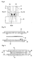
- FIG. 2 shows the configuration of a unit semiconductor device 11 according to the first embodiment.
- the unit semiconductor device 11 comprises a ground substrate 12, a semiconductor element such as a microwave transistor 13, an input terminal 15a, an input-side matching circuit 15b, an output-side matching circuit 15c, and an output terminal 15d.
- the ground substrate 12, i.e., aheat-radiatingground substrate is made of Cu or W and can radiate heat.
- the microwave transistor 13, input terminal 15a, input-side matching circuit 15b, output-side matching circuit 15c and output terminal 15d are provided on the heat-radiating ground substrate 12.
- the semiconductor element is for use at high frequencies. It is, for example, a microwave transistor 13.
- the input terminal 15a and input-side matching circuit 15b are arranged on one side of the microwave transistor 13.
- the output-side matching circuit 15c and output terminal 15d are arranged on the other side of the microwave transistor 13.
- the input terminal 15a and the input-side matching circuit 15b are connected by a lead line, such as gold wire 17a.
- the input-side matching circuit 15b and the microwave transistor 13 are connected by a gold wire 17b.
- the micro wave transistor 13 and the output-side matching circuit 15c are connected by a gold wire 17c.
- the output-side matching circuit 15c and the output terminal 15d are connected by a gold wire 17d.
- the microwave transistor 13 and the matching circuits 15b and 15c are surrounded by a side wall 18. Nonetheless, the input terminal 15a and output terminal 15d are exposed in part.
- FIG. 3 shows, a unit semiconductor device 21 of the same structure as the unit semiconductor device 11 is positioned upside down and laid on the unit semiconductor device 11.
- the device 21 is arranged as indicated by arrow 19, with its sidewall 28 aligned with the sidewall 18 of the unit semiconductor device 11 located below the device 21.
- FIG. 4 the upper edge of the sidewall 28 of the unit semiconductor device 21 abuts on the upper edge of the sidewall 18 of the unit semiconductor device 11.
- the sidewalls 18 and 28 are coupled together at upper edge with of solder made of, for example, a gold-tin alloy.
- FIG. 5 is a side view of the resultant product.
- the upper limit of the frequency range which can be used is determined by the resonance frequency in the cavity. At any frequency higher than the upper limit, the isolation between the terminals is impaired and power is dissipated into the space.
- a1, b1 and c1 be the length, width and height of the cavity of the conventional semiconductor device composed of two parts split in the vertical direction.
- a2, b2 and c2 be the length, width and height of the cavity of the semiconductor device according to the present embodiment. Then, the length a2 and width b2 of the cavity according to the present embodiment will be as shown in FIG. 2 , and the height c2 thereof will be as shown in FIG. 4 .
- Length a1 and length a2 are determined by the matching circuits.
- the unit semiconductor device 21 is laid on the lower unit semiconductor device 11. Therefore, it may be difficult, in some cases, to connect or ground signal lines. This would not happen in the second embodiment.
- the second embodiment will be described below.
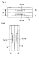
- FIG. 5 shows a combination of the two unit semiconductor devices 11 and 21 according to the first embodiment.
- the second embodiment is such a combination of two unit devices, which is positioned upright and stands on one side as is illustrated in FIG. 6 .
- the devices 11 and 21 have been positioned upright. Then one end of the devices 11 and 21 is embedded in a grounding conductor 33 capable of radiating heat, as is illustrated in FIG. 7 . Thereafter, auxiliary grounding conductors 31 and 32, both able to radiate heat, are secured to the other end of the devices 11 and 21, which are not embedded in the grounding conductor 33. These conductors 31 and 32 are arranged as if clamping those remaining parts of the devices 11 and 21.
- An input-side external circuit 34 is provided on the input side of the grounding conductor 33 capable of radiating heat and is connected to the projecting part 15e of the input terminal 15a.
- an output-side external circuit 37 is provided on the output side of the grounding conductor 33 and is connected to the projecting part 15f of the output terminal 15d.
- FIG. 8 shows this semiconductor device for use at high frequencies, as is viewed from above.
- signal lines can be easily grounded to provide a high-frequency semiconductor device that comprises two unit semiconductor devices.
- FIG. 9 shows the structure of the third embodiment.
- the projecting part 15e of the input terminal 15a and the projecting part 15f of the output terminal 15d, both shown in FIG. 5 are twisted and led outside.
- the projecting part 15f of the output terminal is twisted and let outside.
- the grounding connection is the same as in the embodiment shown in FIG. 7 .
- the projecting part 15e of the input terminal and the input-side external circuit 34 contact in a surface
- the projecting part 15f of the output terminal and the output-side external circuit 37 contact in a surface.
- the embodiment provides a high-frequency semiconductor device in which the signal lines can be easily connected and grounded.
- heat can be efficiently radiated from two surfaces defined by the auxiliary grounding conductors 31 and 32 that have heat-radiating property.
- each high-frequency semiconductor device described above two unit semiconductor devices 11 and 21 are directly coupled, constituting a semiconductor device for use at high frequencies.
- a conductive plate made of metal can be provided between two unit semiconductor devices 11 and 21 in order to prevent microwave interference between the unit semiconductor devices.
- FIGS. 10 and 11 show a high-frequency semiconductor device of such a configuration.
- FIG. 10 is a diagram explaining how a conductive plate 41 is interposed between unit semiconductor devices 11 and 21.
- FIG. 11 is a sectional view of a structure comprising the unit semiconductor devices 11 and 21 secured to each other, with the conductive plate 41 interposed between them.
- the unit semiconductor devices 11 and 21 are identical in configuration to those shown in FIG. 1 .
- This embodiment differs only in that the conductive plate 41 is interposed and secured between the unit semiconductor devices 11 and 21. That is, the conductive plate 41 is laid on the unit semiconductor device 11 so configured as described above and the unit semiconductor device 21 of the same structure as the device 11 is positioned upside down and laid on the conductive plate 41.
- the conductive plate 41 is made of metal. It is desired that the plate 41 should have an expansion coefficient similar to that of the heat-radiating ground substrate 12. Preferably, it should be made of the same material as the heat-radiating ground substrate 12. It is sufficient for the conductive plate 41 to be as large as would cover at least the sidewall 18. It is desired that the plate 41 be thick enough not to allow the passage of microwaves having a wavelength of 5 ⁇ m or more. It may be about 1 mm thick, in consideration of the handling readiness required.
- the sidewall 18 of the upper unit semiconductor device 21 is so arranged that its upper edge is aligned with the upper edge of the sidewall 18 of the lower unit semiconductor device 11, with the conductive plate 41 clamped between the devices 11 and 21.
- the sidewalls of the devices 11 and 21 are coupled and sealed together at upper edge with of solder made of, for example, a gold-tin alloy.
- the resonance frequency can be raised in any mode other than mode TE001, without lowering the resonance frequency of mode TE001.
- FIGS. 14, 15 and 16 show the fifth embodiment. This embodiment differs from the embodiment shown in FIGS. 7, 8 and 9 , only in that a conductive plate 41 is interposed between the two unit semiconductor devices 11 and 21.
- FIG. 13 shows the device that comprises two unit semiconductor devices 11 and 21 and a conductive plate 41 interposed between the devices 11 and 21. As shown in FIG. 14 , this device is positioned upright and stands on one side. Thereafter, auxiliary grounding conductors 31 and 32, both able to radiate heat from the rear surface, are connected and secured to the heat-radiating ground substrates 12 of the device.
- the unit semiconductor devices 11 and 21 are secured to the auxiliary grounding conductors 31 and 32, respectively.
- the conductive plate 41 is clamped between the unit semiconductor devices 11 and the unit semiconductor device 21.
- One end of the two unit semiconductor devices 11 and 21 and the conductive plate 41 is embedded in a grounding conductor 33.
- the grounding conductor 33 is capable of radiating heat (see FIG. 15 ).
- auxiliary grounding conductors 31 and 32 both able to radiate heat, are secured to the other end of the devices 11 and 21, which are not embedded in the grounding conductor 33. These conductors 31 and 32 are arranged as if clamping those remaining parts of the devices 11 and 21.
- An input-side external circuit 34 is provided on the input side of the grounding conductor 33 capable of radiating heat and is connected to the projecting part 15e of the input terminal.
- an output-side external circuit 37 is provided on the output side of the grounding conductor 33 and is connected to the projecting part 15f of the output terminal.
- FIG. 15 shows this high-frequency semiconductor device as viewed from above.
- signal lines can be easily grounded to provide a high-frequency semiconductor device that comprises two unit semiconductor devices and a conductive plate 41 interposed between the unit semiconductor devices.
- heat can be efficiently radiated from two surfaces defined by the auxiliary grounding conductors 31 and 32 that have heat-radiating property.
- FIG. 16 shows the structure of the sixth embodiment. As FIG. 16 shows, the projecting part 15f of the output terminal is twisted and let outside.
- This embodiment is identical to the fifth embodiment shown in FIG. 14 in any other structural respects, such as grounding connection.
- the projecting part 15e of the input terminal and the input-side external circuit 34 contact in a surface
- the projecting part 15f of the output terminal and the output-side external circuit 37 contact in a surface.
- heat can be efficiently radiated from two surfaces defined by the auxiliary grounding conductors 31 and 32 that have heat-radiating property.
- a conductive plate are interposed between the two unit semiconductor devices 11 and 21.
- the conductive plate can therefore prevent microwave interference between the unit semiconductor devices 11 and 21.
- a conventional semiconductor device, the device disclosed in Patent Document 1, and the devices according to the first embodiment and the fourth embodiment were examined for resonance frequency. Theresultswereasshown in Table 1 (for the devices having a cavity of relatively small height) and as shown in Table 2 (for the devices having an cavity of relatively large height).
- the cavity of the device according to this embodiment has length a2 of 1.0 cm, width b2 of 0.5 cm and height c2 of 0.8 cm.
- the cavity of the device according to this embodiment has a height twice the height of the cavity of the conventional device.
- the width of the cavity can yet be half the length. Hence, the resonance frequency in the cavity can be raised.
- the resonance frequency is the same (i.e., 15.0 GHz) in any device examined, irrespective of its configuration.
- mode TE010 and mode TE110 the device according to Patent Document 1 and the devices according to the first and fourth embodiments are advantageous over the conventional semiconductor device (that is, the resonance frequency is higher).
- mode TE001, mode TE101, mode TE011 and mode TE111 only the first embodiment has the opposite effect.
- the resonance frequency is improved in mode TE010 that more adversely influences the isolation characteristic between terminals than any other mode.
- the resonance frequency is not improved inmode TE100, because this mode does not influence the isolation at all.
- the resonance frequency is lower than in the device of the conventional configuration. Nonetheless, in mode TE010 and mode TE110, i.e., two mode which have relatively low resonance frequencies, among the five modes (TE010, TE001, TE110, TE011 and TE111) influencing the isolation, the resonance frequency is two times and 1.5 times as much, respectively.
- the resonance frequency is greatly improved in mode TE010 and mode TE110.
- the cavity may have a comparatively large height. More specifically, the height (c) may be twice as much and greater than the length (a) and the width (b).
- the cavity of the conventional semiconductor device may have length a1 of 1.0 cm, width b1 of 1.0 cm and height c1 of 0.6 cm. In this case, the results are as shown in Table 2.
- mode TE100 the device according to Patent Document 1 and the devices according to the first and fourth embodiments are just the same as the conventional device in terms of resonance frequency.
- mode TE010, mode TE110 and mode TE011 any configuration can raise the resonance frequency over the conventional devices.
- mode TE001 the device according to the first embodiment undergo resonance at lower frequencies than in any other mode.
- mode TE101 and mode TE111 only the first embodiment has the opposite effect.
- the resonance frequency is improved in mode TE101 that more adversely influences the isolation characteristic between terminals than any other mode.
- the resonance frequency is not improved in mode TE100, because this mode does not influence the isolation at all.
- the resonance frequency is lower than in the device of the conventional configuration. Nonetheless, in mode TE010 and mode TE110, i.e., two mode which have relatively low resonance frequencies, among the five modes (TE010, TE001, TE110, TE011 and TE111) influencing the isolation, the resonance frequency is two times and 1.5 times as much, respectively. Thus, the resonance frequency is greatly improved in mode TE010 and mode TE110.
- the resonance frequency can be raised in any mode other than mode TE001, without lowering the resonance frequency of mode TE001.
- the present invention can be applied to any other types of high-frequency semiconductor devices.
- the unit semiconductor devices 11 and 21 need not be sealed at the upper edges of their sidewalls 18 and 28, as long as they are electrically shielded.
- the devices 11 and 21 need not be sealed if their sidewalls 18 and 28 are aligned with each other at upper edge by the conductive plate 41, so long as they are electrically shielded.
- Embodiments of the present invention are not limited to the embodiments described above. Various changes and modifications can be made within the scope and spirit of the invention.
Landscapes
- Microwave Amplifiers (AREA)
- Cooling Or The Like Of Semiconductors Or Solid State Devices (AREA)
- Waveguides (AREA)
Abstract
Description
- The present invention relates to a high-frequency semiconductor device that includes a cavity having a space and semiconductor elements contained in the cavity.
- It is increasingly demanded that semiconductor devices be designed to operate at larger power in, for example, microwave communication. The recent trend is therefore to use larger microwave semiconductor chips and more number of chips in combination. As a result, the cavity containing these chips has become larger. The cut-off frequency, which is determined by the length of cavity in the direction of the orthogonal to the microwave-propagation direction, must be kept at a higher frequency than operating frequencies. The decrease in the cut-off frequency degrades the isolation from the output side to the input side.
- A semiconductor device is known, which is designed to prevent such degradation of the (see Patent Document 1: Jpn. Pat. Appln. Laid-Open Publication No.
5-83010 FIG. 1 ). As shown inFIG. 1 , the cavity of this device is portioned by a grounding conductor, thereby to avoid characteristic degradation such as a decrease in the cut-off frequency. The cavity of this device has length a1, width b1 and height c1 (not shown). That is, this conventional semiconductor device has a plurality of semiconductor elements arranged in the widthwise direction. - This configuration, wherein semiconductor elements are arranged in the widthwise direction, has a problem in respect of radiation of heat because it operates at large power. More precisely, heat cannot be well radiate from the back of the device since many semiconductor elements are arranged in the device package having a small width and inevitably lie close to each other.
- Further, gaps are likely to develop between the package cover and the partition walls provided in the package. Such gaps will degrade the device characteristics. This is one of the causes of the decrease in the device productivity.
- According to an aspect of the present invention, there is provided an example of a high-frequency semiconductor device that includes two unit semiconductor devices. Each unit semiconductor device includes a ground substrate, a high-frequency semiconductor element, an input-side matching circuit, an output-side matching circuit, a side wall member, an input terminal and an output terminal. The ground substrate has heat-radiating property. The high-frequency semiconductor element is provided on the ground substrate. The input-side matching circuit is connected to the high-frequency semiconductor element. The output-side matching circuit is connected to the high-frequency semiconductor element. The side wall member surrounds at least the high-frequency semiconductor element. The input terminal is connected to the input-side matching circuit. The output terminal is connected to the output-side matching circuit. The two unit semiconductor devices are coupled to each other at upper edges of the side wall members.
- According to another aspect of the present invention, there is provided another example of a high-frequency semiconductor device that includes two unit semiconductor devices. Each unit semiconductor device includes a ground substrate, a high-frequency semiconductor element, an input-side matching circuit, an output-side matching circuit, a side wall member, an input terminal, and an output terminal. The ground substrate has heat-radiating property. The high-frequency semiconductor element is provided on the ground substrate. The input-side matching circuit is connected to the high-frequency semiconductor element. The output-side matching circuit is connected to the high-frequency semiconductor element. The side wall member surrounds at least the high-frequency semiconductor element. The input terminal is connected to the output-side matching circuit. The output terminal is connected to the input-side matching circuit. The two unit semiconductor devices are coupled to each other through a conductive plate at upper edges of the side wall members.
-
-
FIG. 1 is a top view showing the configuration of a conventional semiconductor device. -
FIG. 2 is a top view showing the configuration of a unit semiconductor device according to a first embodiment. -
FIG. 3 is a front view explaining how two unit semiconductor devices are coupled to each other in the first embodiment. -
FIG. 4 is a front view showing the two unit semiconductor devices coupled together in the first embodiment. -
FIG. 5 is a side view showing the two unit semiconductor devices coupled together in the first embodiment. -
FIG. 6 is a diagram illustrating the combination of the two unit semiconductor devices (shown inFIG. 5 ) coupled together, which is positioned upright. -
FIG. 7 is a side view of a semiconductor device according to a second embodiment. -
FIG. 8 is a top view of the semiconductor device according to the second embodiment. -
FIG. 9 is a side view of a semiconductor device according to a third embodiment. -
FIG. 10 is a front view explaining how two unit semiconductor devices are coupled to each other in a fourth embodiment. -
FIG. 11 is a front view showing the two unit semiconductor devices coupled together in the fourth embodiment. -
FIG. 12 is a side view showing the two unit semiconductor devices coupled together in the fourth embodiment. -
FIG. 13 is a diagram illustrating the combination of the two unit semiconductor devices (shown inFIG. 12 ) coupled together, which is positioned upright. -
FIG. 14 is a side view of a semiconductor device according to a fifth embodiment. -
FIG. 15 is a top view of the semiconductor device according to the fifth embodiment. -
FIG. 16 is a side view of a semiconductor device according to a sixth embodiment. - The embodiments will be described, with reference to the accompanying drawings. According to the embodiments, two unit semiconductor devices are coupled to each other, one upon the other, constituting a high-frequency semiconductor device.
-
FIG. 2 shows the configuration of aunit semiconductor device 11 according to the first embodiment. Theunit semiconductor device 11 comprises aground substrate 12, a semiconductor element such as amicrowave transistor 13, aninput terminal 15a, an input-side matching circuit 15b, an output-side matching circuit 15c, and anoutput terminal 15d. Theground substrate 12, i.e., aheat-radiatingground substrate, is made of Cu or W and can radiate heat. Themicrowave transistor 13,input terminal 15a, input-side matching circuit 15b, output-side matching circuit 15c andoutput terminal 15d are provided on the heat-radiatingground substrate 12. The semiconductor element is for use at high frequencies. It is, for example, amicrowave transistor 13. Theinput terminal 15a and input-side matching circuit 15b are arranged on one side of themicrowave transistor 13. The output-side matching circuit 15c andoutput terminal 15d are arranged on the other side of themicrowave transistor 13. - The
input terminal 15a and the input-side matching circuit 15b are connected by a lead line, such asgold wire 17a. The input-side matching circuit 15b and themicrowave transistor 13 are connected by agold wire 17b. Themicro wave transistor 13 and the output-side matching circuit 15c are connected by agold wire 17c. The output-side matching circuit 15c and theoutput terminal 15d are connected by agold wire 17d. - As shown in
FIG. 2 , themicrowave transistor 13 and the matchingcircuits side wall 18. Nonetheless, theinput terminal 15a andoutput terminal 15d are exposed in part. - As
FIG. 3 shows, aunit semiconductor device 21 of the same structure as theunit semiconductor device 11 is positioned upside down and laid on theunit semiconductor device 11. Thedevice 21 is arranged as indicated byarrow 19, with itssidewall 28 aligned with thesidewall 18 of theunit semiconductor device 11 located below thedevice 21. - As shown in
FIG. 4 , the upper edge of thesidewall 28 of theunit semiconductor device 21 abuts on the upper edge of thesidewall 18 of theunit semiconductor device 11. Thesidewalls FIG. 5 is a side view of the resultant product. - The upper limit of the frequency range which can be used is determined by the resonance frequency in the cavity. At any frequency higher than the upper limit, the isolation between the terminals is impaired and power is dissipated into the space. Resonance frequency f is expressed as follows:

where a, b and c are the length, width and height of the cavity, respectively, λc is the velocity of light in the atmosphere, and m, n and k are integers. - Resonance frequency f varies with the distribution of the magnetic field generated in the cavity. What are problematical are seven modes, each having a low resonance frequency. The resonance frequencies of these modes are given as follows:


where SQRT is a square root. - Let a1, b1 and c1 be the length, width and height of the cavity of the conventional semiconductor device composed of two parts split in the vertical direction. Similarly, let a2, b2 and c2 be the length, width and height of the cavity of the semiconductor device according to the present embodiment. Then, the length a2 and width b2 of the cavity according to the present embodiment will be as shown in
FIG. 2 , and the height c2 thereof will be as shown inFIG. 4 . - Length a1 and length a2 are determined by the matching circuits. The length of the cavity of this embodiment is the same as that of the cavity of the conventional device. That is, a1 = a2. The width of the cavity is constant, not depending on the number of semiconductor chips provided in the cavity. In the conventional semiconductor device, two chips are arranged side by side. In the present embodiment, one chip is divided into two segments in the widthwise direction, and the cavity is therefore half (1/2) as wide as the cavity of the conventional device. That is, b2 = b1/2.
- The cavity of the embodiment is twice as high as that of the conventional device, because the
unit semiconductor devices - According to the present embodiment, there are two heat-radiating
ground substrates 12, which define external surfaces of the semiconductor device. Heat can therefore be radiated far more readily, compared to the conventional semiconductor device. - In this embodiment, the
unit semiconductor device 21 is laid on the lowerunit semiconductor device 11. Therefore, it may be difficult, in some cases, to connect or ground signal lines. This would not happen in the second embodiment. The second embodiment will be described below. -
FIG. 5 shows a combination of the twounit semiconductor devices FIG. 6 . - The
devices devices grounding conductor 33 capable of radiating heat, as is illustrated inFIG. 7 . Thereafter,auxiliary grounding conductors devices grounding conductor 33. Theseconductors devices external circuit 34 is provided on the input side of the groundingconductor 33 capable of radiating heat and is connected to the projectingpart 15e of theinput terminal 15a. Similarly, an output-sideexternal circuit 37 is provided on the output side of the groundingconductor 33 and is connected to the projectingpart 15f of theoutput terminal 15d. -
FIG. 8 shows this semiconductor device for use at high frequencies, as is viewed from above. As seen fromFIG. 8 , signal lines can be easily grounded to provide a high-frequency semiconductor device that comprises two unit semiconductor devices. - In the second embodiment, it is easy to connect the signal lines to the ground. In addition, heat can be efficiently radiated from two surfaces defined by the
auxiliary grounding conductors - A third embodiment will be described.
FIG. 9 shows the structure of the third embodiment. In this embodiment, the projectingpart 15e of theinput terminal 15a and the projectingpart 15f of theoutput terminal 15d, both shown inFIG. 5 , are twisted and led outside. - As
FIG. 9 shows, the projectingpart 15f of the output terminal is twisted and let outside. The grounding connection is the same as in the embodiment shown inFIG. 7 . In the present embodiment, the projectingpart 15e of the input terminal and the input-sideexternal circuit 34 contact in a surface, and the projectingpart 15f of the output terminal and the output-sideexternal circuit 37 contact in a surface. Thus, the embodiment provides a high-frequency semiconductor device in which the signal lines can be easily connected and grounded. - Also in this embodiment, heat can be efficiently radiated from two surfaces defined by the
auxiliary grounding conductors - In each high-frequency semiconductor device described above, two
unit semiconductor devices - A conductive plate made of metal can be provided between two
unit semiconductor devices -
FIGS. 10 and 11 show a high-frequency semiconductor device of such a configuration.FIG. 10 is a diagram explaining how aconductive plate 41 is interposed betweenunit semiconductor devices FIG. 11 is a sectional view of a structure comprising theunit semiconductor devices conductive plate 41 interposed between them. - The
unit semiconductor devices FIG. 1 . This embodiment differs only in that theconductive plate 41 is interposed and secured between theunit semiconductor devices conductive plate 41 is laid on theunit semiconductor device 11 so configured as described above and theunit semiconductor device 21 of the same structure as thedevice 11 is positioned upside down and laid on theconductive plate 41. - It is good enough if the
conductive plate 41 is made of metal. It is desired that theplate 41 should have an expansion coefficient similar to that of the heat-radiatingground substrate 12. Preferably, it should be made of the same material as the heat-radiatingground substrate 12. It is sufficient for theconductive plate 41 to be as large as would cover at least thesidewall 18. It is desired that theplate 41 be thick enough not to allow the passage of microwaves having a wavelength of 5 µm or more. It may be about 1 mm thick, in consideration of the handling readiness required. - The
sidewall 18 of the upperunit semiconductor device 21 is so arranged that its upper edge is aligned with the upper edge of thesidewall 18 of the lowerunit semiconductor device 11, with theconductive plate 41 clamped between thedevices devices - In the present embodiment with the
conductive plate 41, the resonance frequency can be raised in any mode other than mode TE001, without lowering the resonance frequency of mode TE001. - In the present embodiment, there are two heat-radiating
ground substrates 12, which define external surfaces of the semiconductor device. Heat can therefore be radiated at high efficiency. -
FIGS. 14, 15 and16 show the fifth embodiment. This embodiment differs from the embodiment shown inFIGS. 7, 8 and9 , only in that aconductive plate 41 is interposed between the twounit semiconductor devices FIG. 13 shows the device that comprises twounit semiconductor devices conductive plate 41 interposed between thedevices FIG. 14 , this device is positioned upright and stands on one side. Thereafter,auxiliary grounding conductors ground substrates 12 of the device. - The
unit semiconductor devices auxiliary grounding conductors conductive plate 41 is clamped between theunit semiconductor devices 11 and theunit semiconductor device 21. One end of the twounit semiconductor devices conductive plate 41 is embedded in agrounding conductor 33. The groundingconductor 33 is capable of radiating heat (seeFIG. 15 ). - Thereafter,
auxiliary grounding conductors devices grounding conductor 33. Theseconductors devices external circuit 34 is provided on the input side of the groundingconductor 33 capable of radiating heat and is connected to the projectingpart 15e of the input terminal. Similarly, an output-sideexternal circuit 37 is provided on the output side of the groundingconductor 33 and is connected to the projectingpart 15f of the output terminal. -
FIG. 15 shows this high-frequency semiconductor device as viewed from above. As seen fromFIG. 15 , signal lines can be easily grounded to provide a high-frequency semiconductor device that comprises two unit semiconductor devices and aconductive plate 41 interposed between the unit semiconductor devices. - In the fifth embodiment, heat can be efficiently radiated from two surfaces defined by the
auxiliary grounding conductors - Still another embodiment will be described, with reference to
FIG. 14 . In this embodiment, the projectingpart 15e of the input terminal and the projectingpart 15f of the output terminal, both shown inFIG. 14 , are twisted and led outside.FIG. 16 shows the structure of the sixth embodiment. AsFIG. 16 shows, the projectingpart 15f of the output terminal is twisted and let outside. This embodiment is identical to the fifth embodiment shown inFIG. 14 in any other structural respects, such as grounding connection. - In the present embodiment, the projecting
part 15e of the input terminal and the input-sideexternal circuit 34 contact in a surface, and the projectingpart 15f of the output terminal and the output-sideexternal circuit 37 contact in a surface. Thus, the embodiment provides a high-frequency semiconductor device in which the signal lines can be easily connected and grounded. - In this embodiment, heat can be efficiently radiated from two surfaces defined by the
auxiliary grounding conductors - In the fourth, fifth and sixth embodiments, a conductive plate are interposed between the two
unit semiconductor devices unit semiconductor devices - A conventional semiconductor device, the device disclosed in
Patent Document 1, and the devices according to the first embodiment and the fourth embodiment were examined for resonance frequency. Theresultswereasshown in Table 1 (for the devices having a cavity of relatively small height) and as shown in Table 2 (for the devices having an cavity of relatively large height).Table 1 2c < (a or b) a = 1.0 cm, b = 1.0 cm, c = 0.4 cm (Unit: GHz) Mode Prior Art Patent Document 1 First Embodiment Fourth Embodiment TE100 15.0 15.0 15.0 15.0 TE010 15.0 30.0 30.0 30.0 TE001 75.0 75.0 37.5 75.0 TE110 21.2 33.5 33.5 33.5 TE101 76.5 76.5 40.4 76.5 TE011 76.5 80.8 48.0 80.8 TE111 77.9 82.2 50.3 82.2 Table 2 2c > (a or b) a = 1.0 cm, b = 1.0 cm, c = 0.6 cm (Unit: GHz) Mode Prior Art Patent Document 1 First Embodiment Fourth Embodiment TE100 15.0 15.0 15.0 15.0 TE010 15.0 30.0 30.0 30.0 TE001 25.0 25.0 12.5 25.0 TE110 21.2 33.5 33.5 33.5 TE101 29.2 29.2 19.5 29.2 TE011 29.2 39.1 32.5 39.1 TE111 32.8 41.8 35.8 41.8 - Consider devices whose cavity has a relatively small height (c), even twice as much being less than the length (a) or the width (b). Assume that a conventional device has length a1 of 1.0 cm, width b1 of 1.0 cm and height c1 of 0.4 cm. By contrast, the cavity of the device according to this embodiment has length a2 of 1.0 cm, width b2 of 0.5 cm and height c2 of 0.8 cm. Thus, the cavity of the device according to this embodiment has a height twice the height of the cavity of the conventional device. The width of the cavity can yet be half the length. Hence, the resonance frequency in the cavity can be raised.
- The following can be understood from the results shown in Table 1. In mode TE100, the resonance frequency is the same (i.e., 15.0 GHz) in any device examined, irrespective of its configuration. In mode TE010 and mode TE110, the device according to
Patent Document 1 and the devices according to the first and fourth embodiments are advantageous over the conventional semiconductor device (that is, the resonance frequency is higher). In mode TE001, mode TE101, mode TE011 and mode TE111, only the first embodiment has the opposite effect. - In the device according to the first embodiment that has no conductive plates, the resonance frequency is improved in mode TE010 that more adversely influences the isolation characteristic between terminals than any other mode. The resonance frequency is not improved inmode TE100, because this mode does not influence the isolation at all. In other modes, the resonance frequency is lower than in the device of the conventional configuration. Nonetheless, in mode TE010 and mode TE110, i.e., two mode which have relatively low resonance frequencies, among the five modes (TE010, TE001, TE110, TE011 and TE111) influencing the isolation, the resonance frequency is two times and 1.5 times as much, respectively. Thus, the resonance frequency is greatly improved in mode TE010 and mode TE110.
- The cavity may have a comparatively large height. More specifically, the height (c) may be twice as much and greater than the length (a) and the width (b). For example, the cavity of the conventional semiconductor device may have length a1 of 1.0 cm, width b1 of 1.0 cm and height c1 of 0.6 cm. In this case, the results are as shown in Table 2.
- In mode TE100, the device according to
Patent Document 1 and the devices according to the first and fourth embodiments are just the same as the conventional device in terms of resonance frequency. In mode TE010, mode TE110 and mode TE011, any configuration can raise the resonance frequency over the conventional devices. - In mode TE001, the device according to the first embodiment undergo resonance at lower frequencies than in any other mode. In mode TE101 and mode TE111, only the first embodiment has the opposite effect.
- In the first embodiment without conductive plates, the resonance frequency is improved in mode TE101 that more adversely influences the isolation characteristic between terminals than any other mode. The resonance frequency is not improved in mode TE100, because this mode does not influence the isolation at all. In other modes, the resonance frequency is lower than in the device of the conventional configuration. Nonetheless, in mode TE010 and mode TE110, i.e., two mode which have relatively low resonance frequencies, among the five modes (TE010, TE001, TE110, TE011 and TE111) influencing the isolation, the resonance frequency is two times and 1.5 times as much, respectively. Thus, the resonance frequency is greatly improved in mode TE010 and mode TE110. In mode TE001, whoever, the resonance frequency lowers, and the device according to the first embodiment cannot achieve the advantage desired of it. By contrast, in any device having a conductive plate, the resonance frequency can be raised in any mode other than mode TE001, without lowering the resonance frequency of mode TE001.
- According to the embodiments described above, there are high-frequency semiconductor devices that have microwave transistors. However, the present invention can be applied to any other types of high-frequency semiconductor devices. Further, the
unit semiconductor devices sidewalls devices sidewalls conductive plate 41, so long as they are electrically shielded. - Embodiments of the present invention are not limited to the embodiments described above. Various changes and modifications can be made within the scope and spirit of the invention.
Claims (8)
- A high-frequency semiconductor device comprising two unit semiconductor devices, each of which including:a ground substrate having heat-radiating property;a high-frequency semiconductor element provided on the ground substrate;an input-side matching circuit connected to the high-frequency semiconductor element;an output-side matching circuit connected to the high-frequency semiconductor element;a side wall member surrounding at least the high-frequency semiconductor element;an input terminal connected to the input-side matching circuit; andan output terminal connected to the output-side matching circuit,wherein the two unit semiconductor devices are coupled to each other at an upper edge of the side wall member.
- The high-frequency semiconductor device according to claim 1, further comprising:a grounding conductor in which one end of the two unit semiconductor devices is embedded and which has heat-radiating property;auxiliary grounding conductors having heat-radiating property and configured to clamp the other end of the two unit semiconductor devices;an input-side external circuit which is provided at an input side of the two unit semiconductor devices and is connected to the input terminal; andan output-side external circuit which is provided at an output side of the two unit semiconductor devices and is connected to the output terminal.
- The high-frequency semiconductor device according to claim 2, wherein the input terminal has at least one part twisted and connected to the input-side external circuit.
- The high-frequency semiconductor device according to claim 2, wherein the output terminal has at least one part twisted and connected to the output-side external circuit.
- A high-frequency semiconductor device comprising two unit semiconductor devices, each of which including:a ground substrate having heat-radiating property;a high-frequency semiconductor element provided on the ground substrate;an input-side matching circuit connected to the high-frequency semiconductor element;an output-side matching circuit connected to the high-frequency semiconductor element;a side wall member surrounding at least the high-frequency semiconductor element;an input terminal connected to the input-side matching circuit; andan output terminal connected to the output-side matching circuit,wherein the two unit semiconductor devices are coupled to each other through a conductive plate at an upper edge of the side wall member.
- The high-frequency semiconductor device according to claim 5, further comprising:a grounding conductor in which one end of the two unit semiconductor devices is embedded and which has heat-radiating property;auxiliary grounding conductors having heat-radiating property and configured to clamp the other end of the two unit semiconductor devices;an input-side external circuit which is provided at an input side of the two unit semiconductor devices and is connected to the input terminal; andan output-side external circuit which is provided at an output side of the two unit semiconductor devices and is connected to the output terminal.
- The high-frequency semiconductor device according to claim 6, wherein the input terminal has at least one part twisted and connected to the input-side external circuit.
- The high-frequency semiconductor device according to claim 6, wherein the output terminal has at least one part twisted and connected to the output-side external circuit.
Applications Claiming Priority (2)
| Application Number | Priority Date | Filing Date | Title |
|---|---|---|---|
| JP2006125328 | 2006-04-28 | ||
| PCT/JP2007/000047 WO2007125633A1 (en) | 2006-04-28 | 2007-02-01 | High-frequency semiconductor device |
Publications (2)
| Publication Number | Publication Date |
|---|---|
| EP2015392A1 true EP2015392A1 (en) | 2009-01-14 |
| EP2015392A4 EP2015392A4 (en) | 2011-09-07 |
Family
ID=38655176
Family Applications (1)
| Application Number | Title | Priority Date | Filing Date |
|---|---|---|---|
| EP07706296A Withdrawn EP2015392A4 (en) | 2006-04-28 | 2007-02-01 | HIGH FREQUENCY SEMICONDUCTOR DEVICE |
Country Status (7)
| Country | Link |
|---|---|
| US (2) | US7667322B2 (en) |
| EP (1) | EP2015392A4 (en) |
| JP (1) | JPWO2007125633A1 (en) |
| KR (1) | KR100983855B1 (en) |
| CN (1) | CN101361221A (en) |
| TW (1) | TW200803032A (en) |
| WO (1) | WO2007125633A1 (en) |
Families Citing this family (6)
| Publication number | Priority date | Publication date | Assignee | Title |
|---|---|---|---|---|
| JP5377096B2 (en) | 2008-09-08 | 2013-12-25 | 株式会社東芝 | High frequency package device and manufacturing method thereof |
| US20100091477A1 (en) * | 2008-10-14 | 2010-04-15 | Kabushiki Kaisha Toshiba | Package, and fabrication method for the package |
| JP5631607B2 (en) * | 2009-08-21 | 2014-11-26 | 株式会社東芝 | High frequency circuit having multi-chip module structure |
| CN102832145B (en) * | 2012-08-31 | 2015-04-29 | 中国科学院微电子研究所 | Packaging method of high-frequency internal matching power device |
| JP6273247B2 (en) | 2015-12-03 | 2018-01-31 | 株式会社東芝 | High frequency semiconductor amplifier |
| JP7471538B2 (en) * | 2022-04-28 | 2024-04-19 | 三菱電機株式会社 | Semiconductor Device |
Family Cites Families (24)
| Publication number | Priority date | Publication date | Assignee | Title |
|---|---|---|---|---|
| NL262934A (en) * | 1960-03-30 | |||
| JPS57125505A (en) * | 1981-01-29 | 1982-08-04 | Fujitsu Ltd | Ultrahigh frequency amplifier |
| JPH01283973A (en) * | 1988-05-11 | 1989-11-15 | Hitachi Ltd | Mounting device for photodetecting element |
| JPH03185902A (en) * | 1989-12-14 | 1991-08-13 | Mitsubishi Electric Corp | Semiconductor device |
| JPH04148559A (en) * | 1990-10-11 | 1992-05-21 | Mitsubishi Electric Corp | Hybrid integrated circuit device |
| JP2716605B2 (en) * | 1991-07-31 | 1998-02-18 | 三菱電機株式会社 | Microwave module |
| JPH0583010A (en) * | 1991-09-19 | 1993-04-02 | Nec Corp | Semiconductor device |
| JP2642548B2 (en) * | 1991-09-26 | 1997-08-20 | 株式会社東芝 | Semiconductor device and manufacturing method thereof |
| JPH06151703A (en) * | 1992-11-05 | 1994-05-31 | Sony Corp | Semiconductor device and formation thereof |
| US5545924A (en) * | 1993-08-05 | 1996-08-13 | Honeywell Inc. | Three dimensional package for monolithic microwave/millimeterwave integrated circuits |
| JP2541487B2 (en) * | 1993-11-29 | 1996-10-09 | 日本電気株式会社 | Semiconductor device package |
| JPH0888317A (en) * | 1994-09-14 | 1996-04-02 | Nec Corp | Semiconductor device and its mounting method |
| JPH08130288A (en) * | 1994-10-31 | 1996-05-21 | Toshiba Corp | Semiconductor device |
| KR100186309B1 (en) * | 1996-05-17 | 1999-03-20 | 문정환 | Stacked bottom lead package |
| KR100266637B1 (en) * | 1997-11-15 | 2000-09-15 | 김영환 | Stackable ball grid array semiconductor package and a method thereof |
| US6087723A (en) * | 1998-03-30 | 2000-07-11 | Micron Technology, Inc. | Vertical surface mount assembly and methods |
| US6147411A (en) * | 1998-03-31 | 2000-11-14 | Micron Technology, Inc. | Vertical surface mount package utilizing a back-to-back semiconductor device module |
| JP3479738B2 (en) * | 1998-11-16 | 2003-12-15 | 株式会社アライドマテリアル | Semiconductor package and method of manufacturing heat dissipation substrate used therein |
| JP2001223323A (en) * | 2000-02-10 | 2001-08-17 | Mitsubishi Electric Corp | Semiconductor device |
| JP3662219B2 (en) * | 2001-12-27 | 2005-06-22 | 三菱電機株式会社 | Laminated high frequency module |
| WO2005055317A1 (en) * | 2003-12-05 | 2005-06-16 | Matsushita Electric Industrial Co., Ltd. | Packaged electronic element and method of producing electronic element package |
| JP4134900B2 (en) * | 2003-12-18 | 2008-08-20 | 松下電器産業株式会社 | Electronic device package |
| KR100586698B1 (en) * | 2003-12-23 | 2006-06-08 | 삼성전자주식회사 | Semiconductor Module with Vertically Mounted Semiconductor Chip Package |
| US7242091B2 (en) * | 2005-03-02 | 2007-07-10 | Stats Chippac Ltd. | Stacked semiconductor packages and method therefor |
-
2007
- 2007-02-01 CN CNA2007800015429A patent/CN101361221A/en active Pending
- 2007-02-01 JP JP2008513075A patent/JPWO2007125633A1/en not_active Abandoned
- 2007-02-01 WO PCT/JP2007/000047 patent/WO2007125633A1/en not_active Ceased
- 2007-02-01 EP EP07706296A patent/EP2015392A4/en not_active Withdrawn
- 2007-02-01 KR KR1020087013576A patent/KR100983855B1/en not_active Expired - Fee Related
- 2007-03-07 TW TW096107885A patent/TW200803032A/en not_active IP Right Cessation
- 2007-07-19 US US11/779,904 patent/US7667322B2/en not_active Expired - Fee Related
-
2009
- 2009-12-31 US US12/651,026 patent/US7994637B2/en not_active Expired - Fee Related
Also Published As
| Publication number | Publication date |
|---|---|
| US7667322B2 (en) | 2010-02-23 |
| WO2007125633A1 (en) | 2007-11-08 |
| US20100102443A1 (en) | 2010-04-29 |
| KR20080086978A (en) | 2008-09-29 |
| JPWO2007125633A1 (en) | 2009-09-10 |
| EP2015392A4 (en) | 2011-09-07 |
| US20070290335A1 (en) | 2007-12-20 |
| CN101361221A (en) | 2009-02-04 |
| KR100983855B1 (en) | 2010-09-28 |
| TWI371135B (en) | 2012-08-21 |
| TW200803032A (en) | 2008-01-01 |
| US7994637B2 (en) | 2011-08-09 |
Similar Documents
| Publication | Publication Date | Title |
|---|---|---|
| US5847453A (en) | Microwave circuit package | |
| US7362576B2 (en) | Radio frequency module | |
| US8339204B2 (en) | Semiconductor device | |
| EP0503200A2 (en) | Package for microwave integrated circuit | |
| EP2428989B1 (en) | High-frequency circuit package and high-frequency circuit device | |
| EP1056133A1 (en) | Rf circuit module | |
| EP1307078A2 (en) | High frequency circuit module | |
| US6483406B1 (en) | High-frequency module using slot coupling | |
| US7994637B2 (en) | High-frequency semiconductor device | |
| US20130118010A1 (en) | Packaging for Low-Cost, High-Performance Microwave and Millimeter Wave Modules | |
| EP1250717A2 (en) | Ldmos power package with a plurality of ground signal paths | |
| JPH0210756A (en) | Device for interconnection and protection of microwave chip | |
| JPH07202520A (en) | Microwave circuit | |
| US7026869B2 (en) | Broadband amplifier having offset microstrip section in a housing module | |
| JP2001044717A (en) | Semiconductor device for microwave | |
| JPS60230701A (en) | Radio equipment | |
| ISHITSUKA et al. | A new multilayer ceramic-frame package for high-frequency mmic modules | |
| US20250125286A1 (en) | Semiconductor device | |
| KR101938227B1 (en) | Waveguide package | |
| US20230163085A1 (en) | Semiconductor device | |
| JPH04243154A (en) | Mounting structure of high-frequency planar circuit module | |
| JP2001053508A (en) | Mounting structure of high frequency circuit components | |
| JP2000323595A (en) | Semiconductor device | |
| JP2000133735A (en) | Enclosure for high-frequency integrated circuit | |
| JP2001284490A (en) | High frequency grounding structure |
Legal Events
| Date | Code | Title | Description |
|---|---|---|---|
| PUAI | Public reference made under article 153(3) epc to a published international application that has entered the european phase |
Free format text: ORIGINAL CODE: 0009012 |
|
| 17P | Request for examination filed |
Effective date: 20080613 |
|
| AK | Designated contracting states |
Kind code of ref document: A1 Designated state(s): AT BE BG CH CY CZ DE DK EE ES FI FR GB GR HU IE IS IT LI LT LU LV MC NL PL PT RO SE SI SK TR |
|
| AX | Request for extension of the european patent |
Extension state: AL BA HR MK RS |
|
| DAX | Request for extension of the european patent (deleted) | ||
| RBV | Designated contracting states (corrected) |
Designated state(s): DE FR GB |
|
| A4 | Supplementary search report drawn up and despatched |
Effective date: 20110805 |
|
| RIC1 | Information provided on ipc code assigned before grant |
Ipc: H01L 25/07 20060101ALI20110801BHEP Ipc: H01P 3/08 20060101ALI20110801BHEP Ipc: H01L 23/02 20060101ALI20110801BHEP Ipc: H01P 5/08 20060101AFI20110801BHEP |
|
| STAA | Information on the status of an ep patent application or granted ep patent |
Free format text: STATUS: THE APPLICATION HAS BEEN WITHDRAWN |
|
| 18W | Application withdrawn |
Effective date: 20140707 |