EP2015112A1 - Optical waveguide device - Google Patents
Optical waveguide device Download PDFInfo
- Publication number
- EP2015112A1 EP2015112A1 EP07737808A EP07737808A EP2015112A1 EP 2015112 A1 EP2015112 A1 EP 2015112A1 EP 07737808 A EP07737808 A EP 07737808A EP 07737808 A EP07737808 A EP 07737808A EP 2015112 A1 EP2015112 A1 EP 2015112A1
- Authority
- EP
- European Patent Office
- Prior art keywords
- optical waveguide
- thin plate
- refractive index
- waveguide device
- high refractive
- Prior art date
- Legal status (The legal status is an assumption and is not a legal conclusion. Google has not performed a legal analysis and makes no representation as to the accuracy of the status listed.)
- Granted
Links
Images

Classifications
-
- G—PHYSICS
- G02—OPTICS
- G02B—OPTICAL ELEMENTS, SYSTEMS OR APPARATUS
- G02B6/00—Light guides; Structural details of arrangements comprising light guides and other optical elements, e.g. couplings
- G02B6/10—Light guides; Structural details of arrangements comprising light guides and other optical elements, e.g. couplings of the optical waveguide type
- G02B6/12—Light guides; Structural details of arrangements comprising light guides and other optical elements, e.g. couplings of the optical waveguide type of the integrated circuit kind
- G02B6/122—Basic optical elements, e.g. light-guiding paths
- G02B6/125—Bends, branchings or intersections
-
- G—PHYSICS
- G02—OPTICS
- G02B—OPTICAL ELEMENTS, SYSTEMS OR APPARATUS
- G02B6/00—Light guides; Structural details of arrangements comprising light guides and other optical elements, e.g. couplings
- G02B6/24—Coupling light guides
- G02B6/42—Coupling light guides with opto-electronic elements
- G02B6/4201—Packages, e.g. shape, construction, internal or external details
- G02B6/4204—Packages, e.g. shape, construction, internal or external details the coupling comprising intermediate optical elements, e.g. lenses, holograms
-
- G—PHYSICS
- G02—OPTICS
- G02F—OPTICAL DEVICES OR ARRANGEMENTS FOR THE CONTROL OF LIGHT BY MODIFICATION OF THE OPTICAL PROPERTIES OF THE MEDIA OF THE ELEMENTS INVOLVED THEREIN; NON-LINEAR OPTICS; FREQUENCY-CHANGING OF LIGHT; OPTICAL LOGIC ELEMENTS; OPTICAL ANALOGUE/DIGITAL CONVERTERS
- G02F1/00—Devices or arrangements for the control of the intensity, colour, phase, polarisation or direction of light arriving from an independent light source, e.g. switching, gating or modulating; Non-linear optics
- G02F1/01—Devices or arrangements for the control of the intensity, colour, phase, polarisation or direction of light arriving from an independent light source, e.g. switching, gating or modulating; Non-linear optics for the control of the intensity, phase, polarisation or colour
- G02F1/03—Devices or arrangements for the control of the intensity, colour, phase, polarisation or direction of light arriving from an independent light source, e.g. switching, gating or modulating; Non-linear optics for the control of the intensity, phase, polarisation or colour based on ceramics or electro-optical crystals, e.g. exhibiting Pockels effect or Kerr effect
- G02F1/035—Devices or arrangements for the control of the intensity, colour, phase, polarisation or direction of light arriving from an independent light source, e.g. switching, gating or modulating; Non-linear optics for the control of the intensity, phase, polarisation or colour based on ceramics or electro-optical crystals, e.g. exhibiting Pockels effect or Kerr effect in an optical waveguide structure
Definitions
- the present invention relates to an optimal waveguide device, and more particularly, to an optical waveguide device which uses a thin plate having a thickness of 20 ⁇ m or less and has as least an optical waveguide formed in the thin plate.
- an optical waveguide device in which an optical waveguide or modulation electrodes are formed on a substrate having an electro-optical effect or the like has been often used in the related art.
- the amount of transmitted information tends to increase with the development of multimedia, it is necessary to widen a band of a light modulation frequency.
- an external modulation method using an LN modulator or the like has been proposed.
- Patent Document 1 JP-A-64-18121
- Patent Document 2 JP-A-2003-215519
- Patent Document 1 or 2 LiNbO 3 (hereinafter, referred to as 'LN') is mainly used for the first substrate and a material having a lower dielectric constant than LN, such as quartz, glass, and alumina, is mainly used for the second substrate.
- a material having a lower dielectric constant than LN such as quartz, glass, and alumina
- temperature drift or DC drift according to a temperature change occurs due to a difference between coefficients of linear expansion.
- Patent Document 2 discloses that the first substrate and the second substrate are bonded to each other using an adhesive having a coefficient of linear expansion close to the fist substrate.
- the optical waveguide device is not limited to the light modulator described above.
- the optical waveguide device is requested to have multiple functions, for example, to be used as a diffraction grating or a variable wavelength filter.
- the optical waveguide device is also requested to have high performance, for example, to monitor a control state of the optical waveguide device or an optical integrated circuit, in which a plurality of optical waveguide devices are provided.
- a variable wavelength filter not only an optical waveguide or an electrode is provided in an optical waveguide device, but also a titanium oxide layer and unevenness need to be formed on the optical waveguide in order to form the refractive index distribution which periodically changes along the optical waveguide as disclosed in Patent Document 3 or 4.
- Patent Document 3 JP-A-5-88123
- Patent Document 4 JP-A-5-264809
- optical waveguides need to be bent near an end of a substrate, and accordingly, a reflecting means, such as a green lens, needs to be arranged on the end surface of the substrate.
- a reflecting means such as a green lens
- the number of optical waveguides or electrodes provided in the optical waveguide device increases and various kinds of films, unevenness shape, and the like increase. As a result, the optical waveguide device itself becomes complicated.
- the thin plate is easily damaged due to a difference between coefficients of thermal expansion of the thin plate and each of the members or due to mechanical or thermal stress distortion caused by the complicated shape of the thin plate.
- problems that yield of products decreases, unnecessary stress is applied to the thin plate and an operating characteristic of the optical waveguide device deteriorates, and the like occur.
- an optical waveguide device includes: a thin plate having a thickness of 20 ⁇ m or less; and at least an optical waveguide formed in the thin plate.
- the thin plate is bonded and fixed to a supporting substrate with an adhesive interposed therebetween, and a film haying a higher refractive index than the thin plate and the adhesive is provided on a surface of the thin plate bonded and fixed to the supporting substrate so as to be in contact with or close to at least a part of the optical waveguide.
- 'on a surface' means not only a front surface of the thin plate, but also a front surface after forming a buffer layer, such as an SiO 2 ; film, on the thin plate is include.
- 'being in contact' means not only a state of direct contact, but also indirect contact realized through a buffer layer or the like is included.
- the thin plate is formed of a material having a nonlinear optical effect or an electro-optical effect.
- an electrode or a heater for controlling the intensity, wave front, or a phase of light propagating through the optical waveguide is formed on the other surface of the thin plate not bonded and fixed to the supporting substrate.
- the film having a high refractive index is formed so as to be periodically separated in the guiding direction of the optical waveguide.
- a light detection means for detecting either scattered light from the optical waveguide formed with the film having a high refractive index or led-out light obtained by causing a part of light propagating through the optical waveguide to be led out by means of the film having a high refractive index and a control means for controlling a voltage or a current applied to the electrode on the basis of the amount of light detected by the light detection means are further included, and the intensity, the wave front, or the phase of light propagating through the optical waveguide is controlled.
- the film having a high refractive index is formed in a strip line shape.
- the optical waveguide device includes the thin plate having a thickness of 20 ⁇ m or less and at least an optical waveguide formed in the thin plate, the thin plate is bonded and fixed to a supporting substrate with an adhesive interposed therebetween, and a film having a higher refractive index (hereinafter, referred to as a 'high refractive index film') than the thin plate and the adhesive is provided on a surface of the thin plate bonded and fixed to the supporting substrate so as to be in contact with or close to at least a part of the optical waveguide.
- a 'high refractive index film' a film having a higher refractive index
- the thin plate is formed of a material having a nonlinear optical effect or an electro-optical effect, it becomes possible to provide various kinds of optical waveguide devices, such as an optical harmonic generator, a light modulator, a variable wavelength filter, or an optical switch.
- the electrode or the heater for controlling the intensity, the wave front, or the phase of light propagating through the optical waveguide is formed on the other surface of the thin plate not bonded and fixed to the supporting substrate, it becomes possible to provide various kinds of optical waveguide devices, such as an optical harmonic generator, a light modulator, a variable wavelength filter, or an optical switch.
- the high refractive index film is formed so as to be periodically separated in the guiding direction of the optical waveguide, the high refractive index film can function as a diffraction grating. As a result, it becomes possible to obtain an optical waveguide device, such as a wavelength filter.
- the light detection means for detecting either the scattered light from the optical waveguides formed with the high refractive index film or the led-out light obtained by causing a part of light propagating through the optical waveguide to be led out by means of the high refractive index film and a control means for controlling a voltage or a current applied to the electrode on the basis of the amount of light detected by the light detection means are further included, and the intensity, the wave front, or the phase of light propagating through the optical waveguide is controlled. Accordingly, it becomes possible to provide a high-performance optical waveguide device capable of monitoring a light wave propagating inside the optical waveguide device and controlling a driving state of the optical waveguide device.
- the high refractive index film since the high refractive index film is formed in the strip line shape, the high refractive index film can be used as an opt ical waveguide. Thus, since the high refractive index film can be used as a bent optical waveguide or the like, it becomes possible to provide a high-performance optical waveguide device.
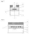
- Fig. 1 shows an optical waveguide device according to an embodiment of the invention.
- Fig. 1 is a cross-sectional view illustrating a light modulation device that include a thin plate 1, which is formed of a material having an electro-optical effect or a nonlinear optical effect and has a thickness of 20 ⁇ m or less, an optical waveguide 2 formed on a front surface of the thin plate, and a control electrode 3 which is formed on the front surface of the thin plate and is used to control light passing through the optical waveguide.
- the optical waveguide 2 may be formed on a bottom surface of the thin plate 1, and a heater may be used instead of the control electrode 3 depending on the type of the optical waveguide device.
- a supporting substrate 5 is bonded to the thin plate 1 with an adhesive 4 interposed there between.
- the optical waveguide 2 can be formed by diffusing, for example, Ti on a substrate surface using a thermal diffusion method, a proton exchange method, or the like.
- the optical waveguide may also be configured by forming a ridge on a front surface of the thin plate 1 according to the shape of the optical waveguide.
- a signal electrode or a grounding electrode or the control electrode 3, such as a DOC electrode, may be formed by formation of an electrode pattern using Ti an Au and a metal plating method, for example.
- Patent Document 5 JP-A-6-289341
- Materials having an electro-optical effect include a lithium niobate, a lithium tantalate, a PLZT (lead lanthanum zirconate titanate), a quartz, and a combination thereof, for example.
- lithium niobate (LN) crystal having a high electro-optical effect is preferably used.
- materials having a nonlinear optical effect include an ADP (ammonium dihydrogen phosphate), Ba 2 NaNb 5 O 15 (barium-sodium niobate), CdSe (cadmium selenide), a KDP (potassium dihydrogen phosphate), LiNbO 3 (lithium niobate), Se (selenium), and Te (tellurium), for example.
- ADP ammonium dihydrogen phosphate
- Ba 2 NaNb 5 O 15 barium-sodium niobate
- CdSe cadmium selenide
- KDP potassium dihydrogen phosphate
- LiNbO 3 lithium niobate
- Se selenium
- Te tellurium
- the optical waveguide described above is formed on a substrate having a thickness of hundreds of micrometers and a bottom surface of the substrate is grinded, thereby forming a thin plate having a thickness of 20 ⁇ m or less.
- a modulation electrode is formed on the front surface of the thin plate.
- the bottom surface of the substrate may be grinded after forming the optical waveguide, the modulation electrode, or the like.
- Various kinds of materials may be used for the supporting substrate 5.
- materials having lower dielectric constants than the thin plate such as a quartz, glass, and an alumina, may be used, or materials having different crystal orientation from the thin plate may also be used as disclosed in Patent Document 4.
- a refractive index of the bonding layer 4 is preferably lower than that of the thin plate 1, especially, that of the optical waveguide 2 in order to suppress a propagation loss of the optical waveguide 2.
- the optical waveguide device is characterized in that a film (high refractive index film) 6, which has a refractive index higher than those of the than plate 1 and an adhesive, is provided on a surface (lower surface of the thin plate shown in Fig. 1 ) of the thin plate 1 bonded and fixed to the supporting substrate 5 so as to be in contact with or close to at least a part of the optical waveguide 2.
- a film (high refractive index film) 6 which has a refractive index higher than those of the than plate 1 and an adhesive, is provided on a surface (lower surface of the thin plate shown in Fig. 1 ) of the thin plate 1 bonded and fixed to the supporting substrate 5 so as to be in contact with or close to at least a part of the optical waveguide 2.
- Fig. 2 is a cross-sectional view illustrating an optical waveguide device according to a first embodiment of the invention and shows an example of the cross-sectional shape of the optical waveguide device taken along a dashed-dotted line A of Fig. 1 .
- High refractive index films 6 are formed on a lower surface of the thin plate 1 at a predetermined period (distance s) therebetween. Due to the shape of such high refractive index film, the high refractive index film functions as a diffraction grating with respect to the optical waveguide 2, and the optical waveguide device can operate as a wavelength filter.
- 'n' is an effective refractive index of a light wave
- 's' is an array period of high refractive index films
- 'm' is a natural number
- the optical waveguide device functions as a variable wavelength filter.
- interaction between the optical waveguide 2 and the high refractive index film 6 may be reinforced by forming the optical waveguide 2 on a bottom surface of the thin plate 1 such that the optical waveguide 2 comes into direct contact with the high refractive index film.
- the thickness of the thin plate 1 is set to 20 ⁇ m or less, especially, to 10 ⁇ m or less, the mode diameter of a light wave propagating through the optical waveguide 2 is almost equal to the thickness of the thin plate 1. Accordingly, even if the optical waveguide is formed on either a front surface or a bottom surface of the thin plate 1, the influence of the contain electrode 3 or the high refractive index film 6 on a light wave propagating through the optical waveguide is equal.
- Fig. 3 is a cross-sectional view illustrating an optical waveguide device according to a second embodiment of the invention and shows an example of the cross-sectional shape of the optical waveguide device taken along the dashed-dotted line A of Fig. 1 .
- the high refractive index film 6 is arranged so as to be in contact with or close to a part of the optical waveguide 2, and a part of electric waves 10 propagating through the optical waveguide 2 is led to the outside of the optical waveguide device as indicated by a dotted line 12. A part of light waves is led to the outside, but the remaining light waves 11 keep propagating through the optical waveguide. Therefore, a state of light waves propagating inside the optical waveguide device can be easily monitored and determined by detecting the led-out light 12 with a photodetector 13.
- the shape of the high refractive index film 6 shown in Fig. 3 is not limited to only the thing of a rectangular parallelepiped. For example, even if the shape is an irregular or indefinite one, a high refractive index film exists near the optical waveguide 2, and accordingly, electric waves that propagate are disordered and a part of light waves is output as scattered light.
- a voltage or a current applied to the control electrode 3 is controlled by a control circuit.
- the intensity, wave front, or a phase of light propagating inside the optical waveguide device is maintained in a predetermined state.
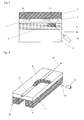
- Fig. 4 illustrates an optical waveguide device according to a third embodiment of the invention.
- the supporting substrate 5 and the bonding layer 4 included in the optical waveguide device are omitted in order to clearly show the appearance of the high refractive index film formed on a surface of the thin plate 1.
- the bonding layer and the supporting substrate are arranged at an upper side of the thin plate 1. shown in Fig. 4 .
- the optical waveguide 2 is formed on a surface of the thin plate 1
- the control electrode 3 is formed on the other surface of the thin plate 1.
- the high refractive index film 6 that is in contact with the optical waveguide 2 and has a strip line shape is formed in a shape shown in Fig. 4 .
- the high refractive index film 6 becomes thick along the optical waveguide 2 and is bent in the middle so as to be separated from the optical waveguide 2.
- the high refractive index film 6 By providing the high refractive index film 6, a part of light waves 20 incident on the optical waveguide 2 moves from the optical waveguide 2 to the high refractive index film 6 and is then output as led-out light 22 from the other end of the high refractive index film 6 to the outside of the optical waveguide device. Since a material having a low refractive index, which serves as a bonding layer, is filled around the high refractive index film 6, the optical waveguide having the high refractive index film 6 as a core is formed. As described above, the led-out light 22 is detected by the photodetector 13 and is used to monitor a state of the optical waveguide device, for example. The remaining light waves that were not led out to the high refractive index film keep propagating through the optical waveguide 2 and are output as output light 21 to the optical waveguide device.
- Fig. 5 illustrates an optical waveguide device according to a fourth embodiment of the invention.
- the electrode 3, the supporting substrate 5, and the bonding layer 4 included in the optical waveguide device are omitted in order to clearly show the appearance of the high refractive index film formed on a surface of the thin plate 1.
- the bonding layer and the supporting substrate are arranged at an upper side of the thin plate 1 shown in Fig. 4 , and the electrode is arranged at a lower side of the thin plate 1.
- Two Mach-Zehnder optical waveguides 2-1 and 2-2 are formed in the thin plate 1.
- the optical waveguide 2-1 and the optical waveguide 2-2 are not connected continuously to each other.
- the high refractive index film 6 that is in contact with the optical waveguides 2-1 and 2-2 and has a strip line shape is formed in a shape shown in Fig. 5 .
- the high refractive index film 6 becomes thick along the optical waveguides 2-1 and 2-2 and is bent such that the optical waveguides 2-1 and 2-2 are connected to each other.
- the high refractive index film 6 By providing the high refractive index film 6, at light waves 30 incident on the optical waveguide 2-1 moves from the optical waveguide 2-1 to the high refractive index film 6 at an end of the optical waveguide 2-1 and is then introduced into the optical waveguide 2-2 from the other end of the high refractive index film 6.
- the light wave introduced into the optical waveguide 2-2 is output as output light 31 of the optical waveguide device to the outside of the optical waveguide device.
- the refractive index of the high refractive index film 6 is higher than that of the optical waveguide 2-1 (or 2-2), and the refractive index of the bonding layer surrounding the high refractive index film 6 is lower than that of the thin plate 1 surrounding the optical waveguide 2-1. Accordingly, the optical waveguides 2-1 and 2-2 can be connected to each other through the high refractive index film 6 with smaller curvature than in a case in which the end of the optical waveguide 2-1 is bent to be connected to the optical waveguide 2-2. With the configuration shown in Fig. 5 , it becomes possible to make an optical integrated circuit, in which a light modulator and the like are integrated, compact.
- semiconductors such as Nb 2 O 5 , TiO 2 , Ta 2 O 5 , As 2 S 3 , and Si, may be preferably used for the high refractive index film 6 described above, and a reactive RF sputtering method may be used when forming the high refractive index film 6.
- an optical waveguide device having multiple functions or high performance, to improve the productivity of products, and to provide an optical waveguide device capable of suppressing deterioration of an operating characteristic of the optical waveguide device.
Landscapes
- Physics & Mathematics (AREA)
- General Physics & Mathematics (AREA)
- Optics & Photonics (AREA)
- Engineering & Computer Science (AREA)
- Nonlinear Science (AREA)
- Chemical & Material Sciences (AREA)
- Ceramic Engineering (AREA)
- Crystallography & Structural Chemistry (AREA)
- Microelectronics & Electronic Packaging (AREA)
- Optical Modulation, Optical Deflection, Nonlinear Optics, Optical Demodulation, Optical Logic Elements (AREA)
- Optical Integrated Circuits (AREA)
Abstract
Description
- The present invention relates to an optimal waveguide device, and more particularly, to an optical waveguide device which uses a thin plate having a thickness of 20 µm or less and has as least an optical waveguide formed in the thin plate.
- In anoptical communication field or an optical measurement field, an optical waveguide device in which an optical waveguide or modulation electrodes are formed on a substrate having an electro-optical effect or the like has been often used in the related art.
In particular, since the amount of transmitted information tends to increase with the development of multimedia, it is necessary to widen a band of a light modulation frequency. In order to realize this, an external modulation method using an LN modulator or the like has been proposed. However, in order to widen the band of the LN modulator, it is necessary to realize speed matching between a light wave and a microwave, which is a modulated signal, and to reduce a driving voltage, - In order to solve the problems, it is known that a condition of speed matching between a microwave and a light wave is satisfied, and at the same time, a driving voltage is reduced by making a substrate thinner than in the related art.
In the followingPatent Document
Patent Document 1:JP-A-64-18121
Patent Document 2:JP-A-2003-215519 - In
Patent Document Patent Document 2 discloses that the first substrate and the second substrate are bonded to each other using an adhesive having a coefficient of linear expansion close to the fist substrate. - On the other hand, use of the optical waveguide device is not limited to the light modulator described above. The optical waveguide device is requested to have multiple functions, for example, to be used as a diffraction grating or a variable wavelength filter. In addition, the optical waveguide device is also requested to have high performance, for example, to monitor a control state of the optical waveguide device or an optical integrated circuit, in which a plurality of optical waveguide devices are provided.
For example, in a variable wavelength filter, not only an optical waveguide or an electrode is provided in an optical waveguide device, but also a titanium oxide layer and unevenness need to be formed on the optical waveguide in order to form the refractive index distribution which periodically changes along the optical waveguide as disclosed inPatent Document
Patent Document 3:JP-A-5-88123
Patent Document 4:JP-A-5-264809 - Moreover, in the optical integrated circuit, optical waveguides need to be bent near an end of a substrate, and accordingly, a reflecting means, such as a green lens, needs to be arranged on the end surface of the substrate. In addition, in order to monitor a light wave propagating through the optical waveguide device, it is necessary to provide an optical waveguide or a directional coupler for monitoring.
Thus, in order to realize an optical waveguide device having multiple functions or high performance, the number of optical waveguides or electrodes provided in the optical waveguide device increases and various kinds of films, unevenness shape, and the like increase. As a result, the optical waveguide device itself becomes complicated. Furthermore, if the members described above are formed on the thin plate described above, the thin plate is easily damaged due to a difference between coefficients of thermal expansion of the thin plate and each of the members or due to mechanical or thermal stress distortion caused by the complicated shape of the thin plate. As a result, problems that yield of products decreases, unnecessary stress is applied to the thin plate and an operating characteristic of the optical waveguide device deteriorates, and the like occur. - In order to solve the problems described above, it is an object of the invention to realize an optical waveguide device having multiple functions or high performance, to improve the productivity of products, and to provide an optical waveguide device capable of suppressing deterioration of an operating characteristic of the optical waveguide device.
- In order to solve the above problems, according to a first aspect or the invention, an optical waveguide device includes: a thin plate having a thickness of 20 µm or less; and at least an optical waveguide formed in the thin plate. The thin plate is bonded and fixed to a supporting substrate with an adhesive interposed therebetween, and a film haying a higher refractive index than the thin plate and the adhesive is provided on a surface of the thin plate bonded and fixed to the supporting substrate so as to be in contact with or close to at least a part of the optical waveguide.
In addition, in the invention, 'on a surface' means not only a front surface of the thin plate, but also a front surface after forming a buffer layer, such as an SiO2; film, on the thin plate is include.
Furthermore, in the invention, 'being in contact' means not only a state of direct contact, but also indirect contact realized through a buffer layer or the like is included. - According to a second aspect of the invention, in the optical waveguide device according to the first aspect, the thin plate is formed of a material having a nonlinear optical effect or an electro-optical effect.
- According to a third aspect of the invention, in the optical waveguide device according to the first or second aspect, an electrode or a heater for controlling the intensity, wave front, or a phase of light propagating through the optical waveguide is formed on the other surface of the thin plate not bonded and fixed to the supporting substrate.
- According to a fourth aspect of the invention, in the optical waveguide device according to any one of the first to third aspects, the film having a high refractive index is formed so as to be periodically separated in the guiding direction of the optical waveguide.
- According to a fifth aspect of the invention, in the optical waveguide device according to the third aspect, a light detection means for detecting either scattered light from the optical waveguide formed with the film having a high refractive index or led-out light obtained by causing a part of light propagating through the optical waveguide to be led out by means of the film having a high refractive index and a control means for controlling a voltage or a current applied to the electrode on the basis of the amount of light detected by the light detection means are further included, and the intensity, the wave front, or the phase of light propagating through the optical waveguide is controlled.
- According to a sixth aspect of the invention, in the optical waveguide device according to any one of the first to third aspects, the film having a high refractive index is formed in a strip line shape.
- According to the first aspect of the invention, the optical waveguide device includes the thin plate having a thickness of 20 µm or less and at least an optical waveguide formed in the thin plate, the thin plate is bonded and fixed to a supporting substrate with an adhesive interposed therebetween, and a film having a higher refractive index (hereinafter, referred to as a 'high refractive index film') than the thin plate and the adhesive is provided on a surface of the thin plate bonded and fixed to the supporting substrate so as to be in contact with or close to at least a part of the optical waveguide. Accordingly, it becomes possible to configure various kinds of members, such as an optical waveguide and a diffraction grating, using the high refractive index film, and it becomes also possible to arrange various kinds of members on both surfaces of the thin plate. As a result, an optical waveguide device having multiple functions and high performance can be easily realized. In addition, since it is possible to suppress local concentration of mechanical or thermal stress in the thin plate, it is possible to prevent the thin plate from being damaged or an operating characteristic of the optical waveguide device from changing. As a result, it becomes possible to provide an optical waveguide device which is excellent in terms of productivity and has an operating characteristic that is stabilized.
- According to the second aspect of the invention, since the thin plate is formed of a material having a nonlinear optical effect or an electro-optical effect, it becomes possible to provide various kinds of optical waveguide devices, such as an optical harmonic generator, a light modulator, a variable wavelength filter, or an optical switch.
- According to the third aspect of the invention, since the electrode or the heater for controlling the intensity, the wave front, or the phase of light propagating through the optical waveguide is formed on the other surface of the thin plate not bonded and fixed to the supporting substrate, it becomes possible to provide various kinds of optical waveguide devices, such as an optical harmonic generator, a light modulator, a variable wavelength filter, or an optical switch.
- According to the fourth aspect of the invention, since the high refractive index film is formed so as to be periodically separated in the guiding direction of the optical waveguide, the high refractive index film can function as a diffraction grating. As a result, it becomes possible to obtain an optical waveguide device, such as a wavelength filter.
- According to the fifth aspect of the invention, the light detection means for detecting either the scattered light from the optical waveguides formed with the high refractive index film or the led-out light obtained by causing a part of light propagating through the optical waveguide to be led out by means of the high refractive index film and a control means for controlling a voltage or a current applied to the electrode on the basis of the amount of light detected by the light detection means are further included, and the intensity, the wave front, or the phase of light propagating through the optical waveguide is controlled. Accordingly, it becomes possible to provide a high-performance optical waveguide device capable of monitoring a light wave propagating inside the optical waveguide device and controlling a driving state of the optical waveguide device.
- According to the sixth aspect of the invention, since the high refractive index film is formed in the strip line shape, the high refractive index film can be used as an opt ical waveguide. Thus, since the high refractive index film can be used as a bent optical waveguide or the like, it becomes possible to provide a high-performance optical waveguide device.
-
- [
Fig. 1] Fig. 1 is a cross-sectional view illustrating an optical waveguide device according to an embodiment of the invention. - [
Fig. 2] Fig. 2 is a cross-sectional view illustrating an optical waveguide device according to a first embodiment of the invention. - [
Fig. 3] Fig. 3 is a cross-sectional view illustrating an optical waveguide device according to a second embodiment of the invention. - [
Fig. 4] Fig. 4 is a perspective view illustrating an optical waveguide device according to a third embodiment of the invention. - [
Fig. 5] Fig. 5 is a perspective view illustrating an optical waveguide device according to a fourth embodiment of the invention. -
- 1: thin plate
- 2: optical waveguide
- 3: modulation electrode
- 4: bonding layer
- 5: supporting substrate
- 6: high refractive index film
- Hereinafter, the invention will be described in derail using preferred examples.
Fig. 1 shows an optical waveguide device according to an embodiment of the invention.Fig. 1 is a cross-sectional view illustrating a light modulation device that include athin plate 1, which is formed of a material having an electro-optical effect or a nonlinear optical effect and has a thickness of 20 µm or less, anoptical waveguide 2 formed on a front surface of the thin plate, and acontrol electrode 3 which is formed on the front surface of the thin plate and is used to control light passing through the optical waveguide. In addition, theoptical waveguide 2 may be formed on a bottom surface of thethin plate 1, and a heater may be used instead of thecontrol electrode 3 depending on the type of the optical waveguide device.
A supportingsubstrate 5 is bonded to thethin plate 1 with an adhesive 4 interposed there between. - As a method of forming the
optical waveguide 2, theoptical waveguide 2 can be formed by diffusing, for example, Ti on a substrate surface using a thermal diffusion method, a proton exchange method, or the like. In addition, as disclosed inPatent Document 5, the optical waveguide may also be configured by forming a ridge on a front surface of thethin plate 1 according to the shape of the optical waveguide.
A signal electrode or a grounding electrode or thecontrol electrode 3, such as a DOC electrode, may be formed by formation of an electrode pattern using Ti an Au and a metal plating method, for example. Moreover, if necessary, it may also be possible to provide a buffer layer (not shown) formed of a dielectric material, such as SiO2, on a substrate surface after forming an optical waveguide and to form a control electrode on the buffer layer.
Patent Document 5:JP-A-6-289341 - Materials having an electro-optical effect include a lithium niobate, a lithium tantalate, a PLZT (lead lanthanum zirconate titanate), a quartz, and a combination thereof, for example. In particular, lithium niobate (LN) crystal having a high electro-optical effect is preferably used.
In addition, materials having a nonlinear optical effect include an ADP (ammonium dihydrogen phosphate), Ba2NaNb5O15 (barium-sodium niobate), CdSe (cadmium selenide), a KDP (potassium dihydrogen phosphate), LiNbO3 (lithium niobate), Se (selenium), and Te (tellurium), for example. - In a method of manufacturing the
thin plate 1 including a light modulation device, the optical waveguide described above is formed on a substrate having a thickness of hundreds of micrometers and a bottom surface of the substrate is grinded, thereby forming a thin plate having a thickness of 20 µm or less. Then, a modulation electrode is formed on the front surface of the thin plate. In addition, the bottom surface of the substrate may be grinded after forming the optical waveguide, the modulation electrode, or the like. In addition, if a thermal impact when forming an optical waveguide or a mechanical impact caused by handling of a thin film in various kinds of processing is applied, there is a risk that a thin plate will be damaged. For this reason, it is preferable to perform processing in which such thermal or mechanical impact is easily applied before grinding a substrate tomake the substrate have a small thickness. - Various kinds of materials may be used for the supporting
substrate 5. For example, in addition to the same material as the thin plate, materials having lower dielectric constants than the thin plate, such as a quartz, glass, and an alumina, may be used, or materials having different crystal orientation from the thin plate may also be used as disclosed inPatent Document 4. In this case, it is preferable to select a material having the same coefficient of linear expansion as the thin plate in order to stabilize a modulation characteristic of a light modulation device with respect to a temperature change. If it is difficult to select the same material, a material having the same coefficient of linear expansion as the thin plate is selected for an adhesive used to bond the thin plate and the supporting substrate as disclosed inPatent Document 2. - In order to bond the
thin plate 1 and the supportingsubstrate 5 to each other, various kinds of adhesive materials, such as an epoxy-based adhesive, a thermosetting adhesive, an ultraviolet curable adhesive, solder glass, a thermosetting resin adhesive sheet, a light curable resin adhesive sheet, or a light-viscosity resin adhesive sheet may be used as thebonding layer 4 . A refractive index of thebonding layer 4 is preferably lower than that of thethin plate 1, especially, that of theoptical waveguide 2 in order to suppress a propagation loss of theoptical waveguide 2. - As shown in
Fig. 1 , the optical waveguide device according to the invention is characterized in that a film (high refractive index film) 6, which has a refractive index higher than those of the thanplate 1 and an adhesive, is provided on a surface (lower surface of the thin plate shown inFig. 1 ) of thethin plate 1 bonded and fixed to the supportingsubstrate 5 so as to be in contact with or close to at least a part of theoptical waveguide 2. - Various kinds of shapes or materials may be used for the high refractive index film according to functions and characteristics of the optical waveguide device. Hereinafter, an embodiment in which a high refractive index film is used will be described.
Fig. 2 is a cross-sectional view illustrating an optical waveguide device according to a first embodiment of the invention and shows an example of the cross-sectional shape of the optical waveguide device taken along a dashed-dotted line A ofFig. 1 .
Highrefractive index films 6 are formed on a lower surface of thethin plate 1 at a predetermined period (distance s) therebetween. Due to the shape of such high refractive index film, the high refractive index film functions as a diffraction grating with respect to theoptical waveguide 2, and the optical waveguide device can operate as a wavelength filter. - A wavelength λ to be selected is determined by the relationship of λ = 2 ns/m (where 'n' is an effective refractive index of a light wave, 's' is an array period of high refractive index films, and 'm' is a natural number). In addition, it is possible to change the wavelength to be selected by changing the intensity of an electric field applied by the
electrode 3. In this case, the optical waveguide device functions as a variable wavelength filter.
In addition, interaction between theoptical waveguide 2 and the highrefractive index film 6 may be reinforced by forming theoptical waveguide 2 on a bottom surface of thethin plate 1 such that theoptical waveguide 2 comes into direct contact with the high refractive index film. Moreover, if necessary, it is also possible to form a thin buffer layer between the highrefractive index film 6 and theoptical waveguide 2 formed on the bottom surface of thethin plate 1. - Furthermore, when the thickness of the
thin plate 1 is set to 20 µm or less, especially, to 10 µm or less, the mode diameter of a light wave propagating through theoptical waveguide 2 is almost equal to the thickness of thethin plate 1. Accordingly, even if the optical waveguide is formed on either a front surface or a bottom surface of thethin plate 1, the influence of the containelectrode 3 or the highrefractive index film 6 on a light wave propagating through the optical waveguide is equal. -
Fig. 3 is a cross-sectional view illustrating an optical waveguide device according to a second embodiment of the invention and shows an example of the cross-sectional shape of the optical waveguide device taken along the dashed-dotted line A ofFig. 1 .
The highrefractive index film 6 is arranged so as to be in contact with or close to a part of theoptical waveguide 2, and a part ofelectric waves 10 propagating through theoptical waveguide 2 is led to the outside of the optical waveguide device as indicated by a dottedline 12. A part of light waves is led to the outside, but the remaininglight waves 11 keep propagating through the optical waveguide. Therefore, a state of light waves propagating inside the optical waveguide device can be easily monitored and determined by detecting the led-out light 12 with aphotodetector 13. - The shape of the high
refractive index film 6 shown inFig. 3 is not limited to only the thing of a rectangular parallelepiped. For example, even if the shape is an irregular or indefinite one, a high refractive index film exists near theoptical waveguide 2, and accordingly, electric waves that propagate are disordered and a part of light waves is output as scattered light. - According to a result detected by the
photodetector 13, a voltage or a current applied to thecontrol electrode 3 is controlled by a control circuit. As a result, the intensity, wave front, or a phase of light propagating inside the optical waveguide device is maintained in a predetermined state. -
Fig. 4 illustrates an optical waveguide device according to a third embodiment of the invention.
InFig. 4 , the supportingsubstrate 5 and thebonding layer 4 included in the optical waveguide device are omitted in order to clearly show the appearance of the high refractive index film formed on a surface of thethin plate 1. In addition, the bonding layer and the supporting substrate are arranged at an upper side of thethin plate 1. shown inFig. 4 .
Theoptical waveguide 2 is formed on a surface of thethin plate 1, and thecontrol electrode 3 is formed on the other surface of thethin plate 1. The highrefractive index film 6 that is in contact with theoptical waveguide 2 and has a strip line shape is formed in a shape shown inFig. 4 . The highrefractive index film 6 becomes thick along theoptical waveguide 2 and is bent in the middle so as to be separated from theoptical waveguide 2. - By providing the high
refractive index film 6, a part oflight waves 20 incident on theoptical waveguide 2 moves from theoptical waveguide 2 to the highrefractive index film 6 and is then output as led-out light 22 from the other end of the highrefractive index film 6 to the outside of the optical waveguide device. Since a material having a low refractive index, which serves as a bonding layer, is filled around the highrefractive index film 6, the optical waveguide having the highrefractive index film 6 as a core is formed.
As described above, the led-out light 22 is detected by thephotodetector 13 and is used to monitor a state of the optical waveguide device, for example. The remaining light waves that were not led out to the high refractive index film keep propagating through theoptical waveguide 2 and are output asoutput light 21 to the optical waveguide device. -
Fig. 5 illustrates an optical waveguide device according to a fourth embodiment of the invention.
InFig. 5 , theelectrode 3, the supportingsubstrate 5, and thebonding layer 4 included in the optical waveguide device are omitted in order to clearly show the appearance of the high refractive index film formed on a surface of thethin plate 1. In addition, the bonding layer and the supporting substrate are arranged at an upper side of thethin plate 1 shown inFig. 4 , and the electrode is arranged at a lower side of thethin plate 1. - Two Mach-Zehnder optical waveguides 2-1 and 2-2 are formed in the
thin plate 1. Here, the optical waveguide 2-1 and the optical waveguide 2-2 are not connected continuously to each other.
On a surface of thethin plate 1, the highrefractive index film 6 that is in contact with the optical waveguides 2-1 and 2-2 and has a strip line shape is formed in a shape shown inFig. 5 . The highrefractive index film 6 becomes thick along the optical waveguides 2-1 and 2-2 and is bent such that the optical waveguides 2-1 and 2-2 are connected to each other. - By providing the high
refractive index film 6, atlight waves 30 incident on the optical waveguide 2-1 moves from the optical waveguide 2-1 to the highrefractive index film 6 at an end of the optical waveguide 2-1 and is then introduced into the optical waveguide 2-2 from the other end of the highrefractive index film 6. The light wave introduced into the optical waveguide 2-2 is output asoutput light 31 of the optical waveguide device to the outside of the optical waveguide device. - The refractive index of the high
refractive index film 6 is higher than that of the optical waveguide 2-1 (or 2-2), and the refractive index of the bonding layer surrounding the highrefractive index film 6 is lower than that of thethin plate 1 surrounding the optical waveguide 2-1. Accordingly, the optical waveguides 2-1 and 2-2 can be connected to each other through the highrefractive index film 6 with smaller curvature than in a case in which the end of the optical waveguide 2-1 is bent to be connected to the optical waveguide 2-2. With the configuration shown inFig. 5 , it becomes possible to make an optical integrated circuit, in which a light modulator and the like are integrated, compact. - For example, semiconductors, such as Nb2O5, TiO2, Ta2O5, As2S3, and Si, may be preferably used for the high
refractive index film 6 described above, and a reactive RF sputtering method may be used when forming the highrefractive index film 6. - As described above, according to the invention, it becomes possible to realize an optical waveguide device having multiple functions or high performance, to improve the productivity of products, and to provide an optical waveguide device capable of suppressing deterioration of an operating characteristic of the optical waveguide device.
Claims (5)
- An optical waveguide device comprising:a thin plate having a thickness of 20 µm or less; andat least an optical waveguide formed in the thin plate,wherein the thin plate is bonded and fixed to a supporting substrate with an adhesive interposed therebetween, anda film having a higher refractive index than the thin plate and the adhesive is provided on a surface of the thin plate bonded and fixed to the supporting substrate so as to be in contact with or close to at least a part of the optical waveguide.
- The optical waveguide device according to claim 1,
wherein the thin plate is formed of a material having a nonlinear optical effect or an electro-optical effect. - The optical waveguide device according to claim 1 or 2,
wherein an electrode or a heater for controlling the intensity, wave front, or a phase of light propagating through the optical waveguide is formed on the other surface of the thin plate not bonded and fixed to the supporting substrate. - The optical waveguide device according to any one of claims 1 to 3, wherein the film having a high refractive index is formed so as to be periodically separated in the guiding direction of the optical waveguide.
- The optical waveguide device according to claim 3, further comprising:a light detection means for detecting either scattered light from the optical waveguide formed with the film having a high refractive index or led-out light obtained by causing a part of light propagating through the optical waveguide to be led out by means of the film having a high refractive index; anda control means for controlling a voltage or a current applied to the electrode on the basis of the amount of light detected by the light detection means,wherein the intensity, the wave front, or the phase of light propagating through the optical waveguide is controlled. 6. The optical waveguide device according to any one of claims 1 to 3,wherein the film having a high refractive index is formed in a strip line shape.
Applications Claiming Priority (2)
| Application Number | Priority Date | Filing Date | Title |
|---|---|---|---|
| JP2006092293A JP4183716B2 (en) | 2006-03-29 | 2006-03-29 | Optical waveguide device |
| PCT/JP2007/054233 WO2007111085A1 (en) | 2006-03-29 | 2007-03-06 | Optical waveguide device |
Publications (3)
| Publication Number | Publication Date |
|---|---|
| EP2015112A1 true EP2015112A1 (en) | 2009-01-14 |
| EP2015112A4 EP2015112A4 (en) | 2009-06-03 |
| EP2015112B1 EP2015112B1 (en) | 2015-09-02 |
Family
ID=38541012
Family Applications (1)
| Application Number | Title | Priority Date | Filing Date |
|---|---|---|---|
| EP07737808.1A Not-in-force EP2015112B1 (en) | 2006-03-29 | 2007-03-06 | Optical waveguide device |
Country Status (4)
| Country | Link |
|---|---|
| US (2) | US8396334B2 (en) |
| EP (1) | EP2015112B1 (en) |
| JP (1) | JP4183716B2 (en) |
| WO (1) | WO2007111085A1 (en) |
Families Citing this family (15)
| Publication number | Priority date | Publication date | Assignee | Title |
|---|---|---|---|---|
| US7759449B2 (en) | 2000-12-15 | 2010-07-20 | Wellman, Inc. | Methods for introducing additives into polyethylene terephthalate |
| JP5071542B2 (en) | 2010-09-30 | 2012-11-14 | 住友大阪セメント株式会社 | Optical waveguide device |
| JP2012078375A (en) * | 2010-09-30 | 2012-04-19 | Sumitomo Osaka Cement Co Ltd | Optical waveguide element |
| JP5472014B2 (en) * | 2010-09-30 | 2014-04-16 | 住友大阪セメント株式会社 | Optical waveguide device and method for manufacturing optical waveguide device |
| JP5685938B2 (en) * | 2010-12-28 | 2015-03-18 | 三菱電機株式会社 | Optical semiconductor device |
| US9529156B2 (en) * | 2012-06-26 | 2016-12-27 | Acacia Communications, Inc. | Cladding defined transmission grating |
| JP5288028B2 (en) * | 2012-07-02 | 2013-09-11 | 住友大阪セメント株式会社 | Optical waveguide device |
| US9575341B2 (en) | 2014-06-28 | 2017-02-21 | Intel Corporation | Solid state LIDAR circuit with waveguides tunable to separate phase offsets |
| US10093523B2 (en) | 2014-10-06 | 2018-10-09 | Warn Industries, Inc. | Programmable controls for a winch |
| US10031286B1 (en) | 2016-06-14 | 2018-07-24 | Onyx Optics, Inc. | Waveguide structures in anisotropic lasing and nonlinear optical media |
| JP2018140698A (en) * | 2017-02-28 | 2018-09-13 | 本田技研工業株式会社 | Vehicle control device |
| US11347126B2 (en) * | 2017-12-26 | 2022-05-31 | Sumitomo Electric Industries, Ltd. | Optical module and process of assembling the same |
| JP7484631B2 (en) * | 2020-09-30 | 2024-05-16 | 住友大阪セメント株式会社 | Optical waveguide element, optical modulation device using the same, and optical transmission device |
| CN112965270B (en) * | 2021-02-05 | 2023-05-16 | 中国电子科技集团公司第四十四研究所 | Lithium niobate thin film double-Y branch optical waveguide modulator adopting curve optical waveguide connection |
| JP7647398B2 (en) * | 2021-07-05 | 2025-03-18 | 富士通オプティカルコンポーネンツ株式会社 | Optical device and optical communication device |
Family Cites Families (18)
| Publication number | Priority date | Publication date | Assignee | Title |
|---|---|---|---|---|
| JPS6418121A (en) | 1987-07-13 | 1989-01-20 | Nippon Telegraph & Telephone | Production of high-speed optical circuit parts |
| JPH05264809A (en) * | 1991-03-14 | 1993-10-15 | Hikari Keisoku Gijutsu Kaihatsu Kk | Diffraction grating and its production |
| JPH0588123A (en) | 1991-09-30 | 1993-04-09 | Hikari Keisoku Gijutsu Kaihatsu Kk | Variable wavelength filter |
| JP3103417B2 (en) | 1992-01-17 | 2000-10-30 | 科学技術振興事業団 | Waveguide type optical demultiplexing circuit |
| JP2574594B2 (en) | 1992-05-26 | 1997-01-22 | 松下電器産業株式会社 | Optical waveguide device and manufacturing method thereof |
| JPH0651254A (en) * | 1992-08-03 | 1994-02-25 | Nippon Telegr & Teleph Corp <Ntt> | Light control device |
| FR2779835A1 (en) * | 1998-06-11 | 1999-12-17 | Centre Nat Rech Scient | LIGHT DIFFRACTION DEVICE BURIED IN MATERIAL |
| JP4443011B2 (en) * | 2000-07-27 | 2010-03-31 | 日本碍子株式会社 | Traveling wave type optical modulator |
| AU2002222205A1 (en) | 2000-12-14 | 2002-06-24 | Bookham Technology Plc | Integrated optical devices |
| JP2002258082A (en) * | 2001-03-02 | 2002-09-11 | Mitsubishi Chemicals Corp | Polymer optical waveguide, method of manufacturing the same, and waveguide type optical switch |
| JP3963313B2 (en) * | 2001-09-05 | 2007-08-22 | 日本碍子株式会社 | Optical waveguide device, optical modulator and optical modulator mounting structure |
| JP4375597B2 (en) * | 2001-11-16 | 2009-12-02 | 日本碍子株式会社 | Optical waveguide device and traveling wave optical modulator |
| US6904186B2 (en) * | 2001-11-16 | 2005-06-07 | Ngk Insulators, Ltd. | Optical modulators and a method for modulating light |
| JP3827629B2 (en) * | 2002-08-30 | 2006-09-27 | 住友大阪セメント株式会社 | Light modulator |
| US7043132B2 (en) * | 2004-01-21 | 2006-05-09 | Fujitsu Limited | Variable optical attenuator having a waveguide and an optically coupled layer with a power monitor |
| EP1769275A1 (en) * | 2004-07-22 | 2007-04-04 | Pirelli & C. S.p.A. | Integrated wavelength selective grating-based filter |
| JP4691428B2 (en) * | 2005-03-31 | 2011-06-01 | 住友大阪セメント株式会社 | Light modulator |
| JP5088123B2 (en) | 2007-12-14 | 2012-12-05 | トヨタ紡織株式会社 | Cushion spring latch structure |
-
2006
- 2006-03-29 JP JP2006092293A patent/JP4183716B2/en not_active Expired - Fee Related
-
2007
- 2007-03-06 EP EP07737808.1A patent/EP2015112B1/en not_active Not-in-force
- 2007-03-06 US US12/225,783 patent/US8396334B2/en not_active Expired - Fee Related
- 2007-03-06 WO PCT/JP2007/054233 patent/WO2007111085A1/en not_active Ceased
-
2011
- 2011-09-26 US US13/200,576 patent/US8391651B2/en not_active Expired - Fee Related
Also Published As
| Publication number | Publication date |
|---|---|
| US8391651B2 (en) | 2013-03-05 |
| US20120020607A1 (en) | 2012-01-26 |
| US20090116781A1 (en) | 2009-05-07 |
| US8396334B2 (en) | 2013-03-12 |
| EP2015112B1 (en) | 2015-09-02 |
| WO2007111085A1 (en) | 2007-10-04 |
| EP2015112A4 (en) | 2009-06-03 |
| JP2007264488A (en) | 2007-10-11 |
| JP4183716B2 (en) | 2008-11-19 |
Similar Documents
| Publication | Publication Date | Title |
|---|---|---|
| US8396334B2 (en) | Optical waveguide device | |
| US8644647B2 (en) | Optical control device | |
| EP2141532B1 (en) | Optical modulator device based on the electro-optic effect | |
| US8923658B2 (en) | Optical waveguide device | |
| EP2136241B1 (en) | Optical modulator device based on the electro-optic effect | |
| US8600197B2 (en) | Optical control device | |
| EP2485081A1 (en) | Optical waveguide element | |
| US20100247024A1 (en) | Optical waveguide type device | |
| US7912325B2 (en) | Optical control element | |
| US20100296767A1 (en) | Optical modulator | |
| CN100447615C (en) | Optical waveguide device and traveling wave type optical modulator | |
| US6950218B2 (en) | Optical modulator | |
| JP2001350046A (en) | Integrated optical waveguide element | |
| JPH05297332A (en) | Optical modulator | |
| JP4544474B2 (en) | Light modulator | |
| JPH05297333A (en) | Optical modulator | |
| US7409114B2 (en) | Optical modulator | |
| JP7861632B2 (en) | Optical waveguide element, optical modulation device using the same, and optical transmission device | |
| JP2006309124A (en) | Optical modulator | |
| JP4671335B2 (en) | Waveguide type optical device | |
| WO2024201876A1 (en) | Optical waveguide element and optical modulation device using same, and optical transmission device | |
| JPH06337385A (en) | Optical waveguide module |
Legal Events
| Date | Code | Title | Description |
|---|---|---|---|
| PUAI | Public reference made under article 153(3) epc to a published international application that has entered the european phase |
Free format text: ORIGINAL CODE: 0009012 |
|
| 17P | Request for examination filed |
Effective date: 20081027 |
|
| AK | Designated contracting states |
Kind code of ref document: A1 Designated state(s): AT BE BG CH CY CZ DE DK EE ES FI FR GB GR HU IE IS IT LI LT LU LV MC MT NL PL PT RO SE SI SK TR |
|
| AX | Request for extension of the european patent |
Extension state: AL BA HR MK RS |
|
| A4 | Supplementary search report drawn up and despatched |
Effective date: 20090507 |
|
| 17Q | First examination report despatched |
Effective date: 20090715 |
|
| DAX | Request for extension of the european patent (deleted) | ||
| GRAP | Despatch of communication of intention to grant a patent |
Free format text: ORIGINAL CODE: EPIDOSNIGR1 |
|
| RIC1 | Information provided on ipc code assigned before grant |
Ipc: G02F 1/035 20060101ALI20150216BHEP Ipc: G02B 6/12 20060101AFI20150216BHEP Ipc: G02F 1/365 20060101ALI20150216BHEP |
|
| INTG | Intention to grant announced |
Effective date: 20150319 |
|
| GRAS | Grant fee paid |
Free format text: ORIGINAL CODE: EPIDOSNIGR3 |
|
| GRAA | (expected) grant |
Free format text: ORIGINAL CODE: 0009210 |
|
| AK | Designated contracting states |
Kind code of ref document: B1 Designated state(s): AT BE BG CH CY CZ DE DK EE ES FI FR GB GR HU IE IS IT LI LT LU LV MC MT NL PL PT RO SE SI SK TR |
|
| REG | Reference to a national code |
Ref country code: GB Ref legal event code: FG4D |
|
| REG | Reference to a national code |
Ref country code: AT Ref legal event code: REF Ref document number: 746982 Country of ref document: AT Kind code of ref document: T Effective date: 20150915 Ref country code: CH Ref legal event code: EP |
|
| REG | Reference to a national code |
Ref country code: IE Ref legal event code: FG4D |
|
| REG | Reference to a national code |
Ref country code: DE Ref legal event code: R096 Ref document number: 602007042891 Country of ref document: DE |
|
| REG | Reference to a national code |
Ref country code: AT Ref legal event code: MK05 Ref document number: 746982 Country of ref document: AT Kind code of ref document: T Effective date: 20150902 |
|
| PG25 | Lapsed in a contracting state [announced via postgrant information from national office to epo] |
Ref country code: GR Free format text: LAPSE BECAUSE OF FAILURE TO SUBMIT A TRANSLATION OF THE DESCRIPTION OR TO PAY THE FEE WITHIN THE PRESCRIBED TIME-LIMIT Effective date: 20151203 Ref country code: LV Free format text: LAPSE BECAUSE OF FAILURE TO SUBMIT A TRANSLATION OF THE DESCRIPTION OR TO PAY THE FEE WITHIN THE PRESCRIBED TIME-LIMIT Effective date: 20150902 Ref country code: FI Free format text: LAPSE BECAUSE OF FAILURE TO SUBMIT A TRANSLATION OF THE DESCRIPTION OR TO PAY THE FEE WITHIN THE PRESCRIBED TIME-LIMIT Effective date: 20150902 Ref country code: LT Free format text: LAPSE BECAUSE OF FAILURE TO SUBMIT A TRANSLATION OF THE DESCRIPTION OR TO PAY THE FEE WITHIN THE PRESCRIBED TIME-LIMIT Effective date: 20150902 |
|
| REG | Reference to a national code |
Ref country code: LT Ref legal event code: MG4D Ref country code: NL Ref legal event code: MP Effective date: 20150902 |
|
| PG25 | Lapsed in a contracting state [announced via postgrant information from national office to epo] |
Ref country code: SE Free format text: LAPSE BECAUSE OF FAILURE TO SUBMIT A TRANSLATION OF THE DESCRIPTION OR TO PAY THE FEE WITHIN THE PRESCRIBED TIME-LIMIT Effective date: 20150902 Ref country code: PL Free format text: LAPSE BECAUSE OF FAILURE TO SUBMIT A TRANSLATION OF THE DESCRIPTION OR TO PAY THE FEE WITHIN THE PRESCRIBED TIME-LIMIT Effective date: 20150902 Ref country code: ES Free format text: LAPSE BECAUSE OF FAILURE TO SUBMIT A TRANSLATION OF THE DESCRIPTION OR TO PAY THE FEE WITHIN THE PRESCRIBED TIME-LIMIT Effective date: 20150902 Ref country code: AT Free format text: LAPSE BECAUSE OF FAILURE TO SUBMIT A TRANSLATION OF THE DESCRIPTION OR TO PAY THE FEE WITHIN THE PRESCRIBED TIME-LIMIT Effective date: 20150902 |
|
| REG | Reference to a national code |
Ref country code: FR Ref legal event code: PLFP Year of fee payment: 10 |
|
| PG25 | Lapsed in a contracting state [announced via postgrant information from national office to epo] |
Ref country code: EE Free format text: LAPSE BECAUSE OF FAILURE TO SUBMIT A TRANSLATION OF THE DESCRIPTION OR TO PAY THE FEE WITHIN THE PRESCRIBED TIME-LIMIT Effective date: 20150902 Ref country code: CZ Free format text: LAPSE BECAUSE OF FAILURE TO SUBMIT A TRANSLATION OF THE DESCRIPTION OR TO PAY THE FEE WITHIN THE PRESCRIBED TIME-LIMIT Effective date: 20150902 Ref country code: IT Free format text: LAPSE BECAUSE OF FAILURE TO SUBMIT A TRANSLATION OF THE DESCRIPTION OR TO PAY THE FEE WITHIN THE PRESCRIBED TIME-LIMIT Effective date: 20150902 Ref country code: IS Free format text: LAPSE BECAUSE OF FAILURE TO SUBMIT A TRANSLATION OF THE DESCRIPTION OR TO PAY THE FEE WITHIN THE PRESCRIBED TIME-LIMIT Effective date: 20160102 Ref country code: SK Free format text: LAPSE BECAUSE OF FAILURE TO SUBMIT A TRANSLATION OF THE DESCRIPTION OR TO PAY THE FEE WITHIN THE PRESCRIBED TIME-LIMIT Effective date: 20150902 Ref country code: NL Free format text: LAPSE BECAUSE OF FAILURE TO SUBMIT A TRANSLATION OF THE DESCRIPTION OR TO PAY THE FEE WITHIN THE PRESCRIBED TIME-LIMIT Effective date: 20150902 |
|
| PG25 | Lapsed in a contracting state [announced via postgrant information from national office to epo] |
Ref country code: RO Free format text: LAPSE BECAUSE OF FAILURE TO SUBMIT A TRANSLATION OF THE DESCRIPTION OR TO PAY THE FEE WITHIN THE PRESCRIBED TIME-LIMIT Effective date: 20150902 Ref country code: PT Free format text: LAPSE BECAUSE OF FAILURE TO SUBMIT A TRANSLATION OF THE DESCRIPTION OR TO PAY THE FEE WITHIN THE PRESCRIBED TIME-LIMIT Effective date: 20160104 |
|
| REG | Reference to a national code |
Ref country code: DE Ref legal event code: R097 Ref document number: 602007042891 Country of ref document: DE |
|
| PLBE | No opposition filed within time limit |
Free format text: ORIGINAL CODE: 0009261 |
|
| STAA | Information on the status of an ep patent application or granted ep patent |
Free format text: STATUS: NO OPPOSITION FILED WITHIN TIME LIMIT |
|
| 26N | No opposition filed |
Effective date: 20160603 |
|
| PG25 | Lapsed in a contracting state [announced via postgrant information from national office to epo] |
Ref country code: SI Free format text: LAPSE BECAUSE OF FAILURE TO SUBMIT A TRANSLATION OF THE DESCRIPTION OR TO PAY THE FEE WITHIN THE PRESCRIBED TIME-LIMIT Effective date: 20150902 Ref country code: DK Free format text: LAPSE BECAUSE OF FAILURE TO SUBMIT A TRANSLATION OF THE DESCRIPTION OR TO PAY THE FEE WITHIN THE PRESCRIBED TIME-LIMIT Effective date: 20150902 Ref country code: BE Free format text: LAPSE BECAUSE OF NON-PAYMENT OF DUE FEES Effective date: 20160331 |
|
| PG25 | Lapsed in a contracting state [announced via postgrant information from national office to epo] |
Ref country code: MC Free format text: LAPSE BECAUSE OF FAILURE TO SUBMIT A TRANSLATION OF THE DESCRIPTION OR TO PAY THE FEE WITHIN THE PRESCRIBED TIME-LIMIT Effective date: 20150902 Ref country code: LU Free format text: LAPSE BECAUSE OF FAILURE TO SUBMIT A TRANSLATION OF THE DESCRIPTION OR TO PAY THE FEE WITHIN THE PRESCRIBED TIME-LIMIT Effective date: 20160306 |
|
| REG | Reference to a national code |
Ref country code: CH Ref legal event code: PL |
|
| GBPC | Gb: european patent ceased through non-payment of renewal fee |
Effective date: 20160306 |
|
| REG | Reference to a national code |
Ref country code: IE Ref legal event code: MM4A |
|
| PG25 | Lapsed in a contracting state [announced via postgrant information from national office to epo] |
Ref country code: BE Free format text: LAPSE BECAUSE OF FAILURE TO SUBMIT A TRANSLATION OF THE DESCRIPTION OR TO PAY THE FEE WITHIN THE PRESCRIBED TIME-LIMIT Effective date: 20150902 |
|
| PG25 | Lapsed in a contracting state [announced via postgrant information from national office to epo] |
Ref country code: IE Free format text: LAPSE BECAUSE OF NON-PAYMENT OF DUE FEES Effective date: 20160306 Ref country code: LI Free format text: LAPSE BECAUSE OF NON-PAYMENT OF DUE FEES Effective date: 20160331 Ref country code: CH Free format text: LAPSE BECAUSE OF NON-PAYMENT OF DUE FEES Effective date: 20160331 Ref country code: GB Free format text: LAPSE BECAUSE OF NON-PAYMENT OF DUE FEES Effective date: 20160306 |
|
| REG | Reference to a national code |
Ref country code: FR Ref legal event code: PLFP Year of fee payment: 11 |
|
| PG25 | Lapsed in a contracting state [announced via postgrant information from national office to epo] |
Ref country code: MT Free format text: LAPSE BECAUSE OF FAILURE TO SUBMIT A TRANSLATION OF THE DESCRIPTION OR TO PAY THE FEE WITHIN THE PRESCRIBED TIME-LIMIT Effective date: 20150902 |
|
| REG | Reference to a national code |
Ref country code: FR Ref legal event code: PLFP Year of fee payment: 12 |
|
| PG25 | Lapsed in a contracting state [announced via postgrant information from national office to epo] |
Ref country code: CY Free format text: LAPSE BECAUSE OF FAILURE TO SUBMIT A TRANSLATION OF THE DESCRIPTION OR TO PAY THE FEE WITHIN THE PRESCRIBED TIME-LIMIT Effective date: 20150902 Ref country code: HU Free format text: LAPSE BECAUSE OF FAILURE TO SUBMIT A TRANSLATION OF THE DESCRIPTION OR TO PAY THE FEE WITHIN THE PRESCRIBED TIME-LIMIT; INVALID AB INITIO Effective date: 20070306 |
|
| PG25 | Lapsed in a contracting state [announced via postgrant information from national office to epo] |
Ref country code: TR Free format text: LAPSE BECAUSE OF FAILURE TO SUBMIT A TRANSLATION OF THE DESCRIPTION OR TO PAY THE FEE WITHIN THE PRESCRIBED TIME-LIMIT Effective date: 20150902 Ref country code: MT Free format text: LAPSE BECAUSE OF FAILURE TO SUBMIT A TRANSLATION OF THE DESCRIPTION OR TO PAY THE FEE WITHIN THE PRESCRIBED TIME-LIMIT Effective date: 20160331 |
|
| PG25 | Lapsed in a contracting state [announced via postgrant information from national office to epo] |
Ref country code: BG Free format text: LAPSE BECAUSE OF FAILURE TO SUBMIT A TRANSLATION OF THE DESCRIPTION OR TO PAY THE FEE WITHIN THE PRESCRIBED TIME-LIMIT Effective date: 20150902 |
|
| PGFP | Annual fee paid to national office [announced via postgrant information from national office to epo] |
Ref country code: FR Payment date: 20230322 Year of fee payment: 17 |
|
| PGFP | Annual fee paid to national office [announced via postgrant information from national office to epo] |
Ref country code: DE Payment date: 20230321 Year of fee payment: 17 |
|
| P01 | Opt-out of the competence of the unified patent court (upc) registered |
Effective date: 20230527 |
|
| REG | Reference to a national code |
Ref country code: DE Ref legal event code: R082 Ref document number: 602007042891 Country of ref document: DE Representative=s name: SONNENBERG HARRISON PARTNERSCHAFT MBB PATENT- , DE |
|
| REG | Reference to a national code |
Ref country code: DE Ref legal event code: R119 Ref document number: 602007042891 Country of ref document: DE |
|
| PG25 | Lapsed in a contracting state [announced via postgrant information from national office to epo] |
Ref country code: DE Free format text: LAPSE BECAUSE OF NON-PAYMENT OF DUE FEES Effective date: 20241001 |
|
| PG25 | Lapsed in a contracting state [announced via postgrant information from national office to epo] |
Ref country code: FR Free format text: LAPSE BECAUSE OF NON-PAYMENT OF DUE FEES Effective date: 20240331 |
|
| PG25 | Lapsed in a contracting state [announced via postgrant information from national office to epo] |
Ref country code: FR Free format text: LAPSE BECAUSE OF NON-PAYMENT OF DUE FEES Effective date: 20240331 Ref country code: DE Free format text: LAPSE BECAUSE OF NON-PAYMENT OF DUE FEES Effective date: 20241001 |