EP2012250A2 - Diviseur analogique - Google Patents
Diviseur analogique Download PDFInfo
- Publication number
- EP2012250A2 EP2012250A2 EP08103649A EP08103649A EP2012250A2 EP 2012250 A2 EP2012250 A2 EP 2012250A2 EP 08103649 A EP08103649 A EP 08103649A EP 08103649 A EP08103649 A EP 08103649A EP 2012250 A2 EP2012250 A2 EP 2012250A2
- Authority
- EP
- European Patent Office
- Prior art keywords
- signal
- triangular
- input voltage
- sawtooth
- voltage
- Prior art date
- Legal status (The legal status is an assumption and is not a legal conclusion. Google has not performed a legal analysis and makes no representation as to the accuracy of the status listed.)
- Granted
Links
Images







Classifications
-
- G—PHYSICS
- G06—COMPUTING OR CALCULATING; COUNTING
- G06G—ANALOGUE COMPUTERS
- G06G7/00—Devices in which the computing operation is performed by varying electric or magnetic quantities
- G06G7/12—Arrangements for performing computing operations, e.g. operational amplifiers specially adapted therefor
- G06G7/16—Arrangements for performing computing operations, e.g. operational amplifiers specially adapted therefor for multiplication or division
-
- G—PHYSICS
- G06—COMPUTING OR CALCULATING; COUNTING
- G06G—ANALOGUE COMPUTERS
- G06G7/00—Devices in which the computing operation is performed by varying electric or magnetic quantities
- G06G7/12—Arrangements for performing computing operations, e.g. operational amplifiers specially adapted therefor
- G06G7/16—Arrangements for performing computing operations, e.g. operational amplifiers specially adapted therefor for multiplication or division
- G06G7/161—Arrangements for performing computing operations, e.g. operational amplifiers specially adapted therefor for multiplication or division with pulse modulation, e.g. modulation of amplitude, width, frequency, phase or form
Definitions
- the invention relates to a method for operating an analog divider, wherein a sawtooth or triangular signal is formed, for generating a first input voltage as a divisor and a reference potential are given, and wherein said sawtooth or triangular signal by means of a first comparator with a second input voltage as Dividend is compared in such a way that as a first comparison signal, a pulse width modulated signal is generated, the average value is output as a quotient of the division. Furthermore, the invention relates to an analog divider for carrying out the method.
- Analog dividers are circuits that are mainly used in control engineering. For example, in electric devices that are power-controlled, a quotient formation is required in order to determine a desired current from a predetermined power and a measured voltage. Another application is in the control of complex clocked converters with two pole positions. In this case, an input voltage and an output voltage are measured and derived according to the type of the converter, a duty cycle size, for example, by dividing the output voltage by the sum of input and output voltage.
- analogue dividers are known, by means of which an output voltage is derived from two input voltages, which corresponds to the quotient of the division of the two input voltages.
- operational amplifiers are used. These operational amplifiers are with appropriate wiring as logic devices such For example, subtractor, logarithm or De-logarithmier formed.
- An analog divider is then composed, for example, of two logarithmers, a subtractor and a de-logarithm (cf. Fig. 1 ).
- JP 2005 157 721 A1 In order to reduce the influence of the component tolerance, is in the JP 2005 157 721 A1 indicated a circuit in which a first input voltage is supplied as a divisor a sawtooth or triangular generator. This generator forms a sawtooth or triangular signal, wherein the value of the first input voltage is specified as a positive peak value of the signal. In a subsequent comparator, this sawtooth or triangular signal is compared with a second input voltage. As a comparison signal is obtained while a pulse width modulated signal, the average value is output as the quotient of the division of the second by the first input voltage.
- a sawtooth or triangular generator comprises components whose tolerances in turn lead to inaccuracies. According to the prior art, such circuits are therefore calibrated, but this is associated with considerable effort. In addition, a one-time calibration is not suitable, for example, to reduce inaccuracies due to a temperature drift of individual components.
- Circuit arrangements are also known for generating a sawtooth or triangular signal, in which further comparators are arranged in such a way that the influence of individual components is eliminated.
- a reference voltage is generally generated which is proportional to the first input voltage (see. Fig. 4 ).
- a known circuit arrangement of a triangular signal generator comprises two comparators and a capacitor to which the triangular signal is applied.
- one comparator compares the triangular signal with the first input voltage and the other comparator compares the triangular signal with a reference potential.
- a controller switches the capacitor alternately to a current source and a current sink (see. Fig. 5 ).
- Another circuit arrangement for generating a triangular signal has a similar structure, but instead of the current source and the current sink comprises a positive and a negative voltage source.
- the switching element for switching between positive and negative voltage source then an example designed as a wired operational amplifier integrator is connected to the output of the triangular signal can be tapped (see. Fig. 6 ).
- a triangular signal generated in this way has the disadvantage that due to the response times of the comparators delays in the switching of the switching element occur, which lead to an inaccurate triangular signal (see. Fig. 7 and 8th ). As a result, the quotient of the division is also error-prone.
- the invention has for its object to provide an improvement over the prior art for an analog divider of the type mentioned.
- the sawtooth or triangular signal is formed by means of a first and a second regulator, and the first regulator (REG1) is supplied with the first input voltage (U1) or a voltage proportional thereto and the sawtooth or triangular signal or a signal proportional thereto in such a way that the upper peak value of the sawtooth or triangular signal of the first input voltage is readjusted. Furthermore, the second controller (REG2) is supplied with the reference potential and the sawtooth or triangular signal in such a way that the lower Peak value of the sawtooth or triangular signal is readjusted to the value of the reference potential.
- the sawtooth or triangular generator provides a signal that over the prior art leads to higher accuracies in analog dividers.
- a control signal is formed by means of the first controller as the upper nominal peak value, and this actuating signal is supplied to a second comparator for comparison with the sawtooth or triangular signal. Furthermore, by means of a second controller an actuating signal is formed as a lower desired peak value and this actuating signal is fed to a third comparator for comparison with the sawtooth or triangular signal.
- the second comparison signal at the output of the second comparator and the third comparison signal at the output of the third comparator are fed to a controller, by means of which the charging and discharging of a capacitor to form the sawtooth or triangular signal is controlled.
- the comparators are thus given the control signals of the controller for comparison with the triangular signal. In this way one obtains two controlled systems for generating a triangular signal whose peak values correspond exactly to the desired values.
- the actuating signal of the first regulator is formed from the deviation of the upper actual peak value of the triangular signal from the first input voltage and the actuating signal of the second regulator is formed from the deviation of the lower actual peak value of the triangular signal from the reference potential.
- the first controller provides a lower control signal when the upper actual peak of the triangular signal rises above the value of the first input voltage.
- the upper actual peak value falls of the triangular signal below the value of the first input voltage, the first controller gives a higher control signal.
- a method for high first input voltages, a method is provided in which the control signal of the first controller from the deviation of the means of the low-pass filter averaged triangle signal of half the first input voltage is formed and in which the control signal of the second controller from the deviation of the lower actual peak value of the triangular signal from Reference potential is formed.
- the first input voltage applied to the first regulator is thus halved, which is why a regulator with a lower permissible input voltage can be used for this process.
- an analog divider to which a first input voltage as a divisor and a second input voltage as a dividend are supplied and which comprises a sawtooth or triangular generator, to which the first input voltage is predetermined as the upper peak value of a generated sawtooth or triangular signal, wherein the output of the shege leopard- or triangular generator is connected to an input of a first comparator, which is also fed to the second input voltage, so that at the output of the first comparator a pulse width modulated signal is applied as a first comparison signal of the sawtooth or triangular signal and the second input voltage and a smoothing unit is supplied to the output of which the averaged pulse width modulated signal is applied as a quotient of the division and can be tapped off as an output voltage is.
- the controller comprises a latch, to which the second and third comparison signal are supplied and by means of which a switching element is activated which turns on the capacitor alternately to a positive power source and a negative power source. In this way, a simple circuit for generating a stable triangular signal is given.
- the frequency of the triangular signal is independent of the height of the first input voltage. This is achieved by the current source providing a positive current formed of the first input voltage times a positive coefficient, and the current sink providing a negative current formed of the first input voltage times a negative coefficient.
- the first comparison signal is fed via a first low-pass filter to a third controller whose output is connected to a second low-pass filter and that the voltage applied to the output of the second low-pass filter output voltage is in turn fed to the third controller as a controlled variable ,
- the quotient of the division output an output voltage that adapts very quickly to changes in the first or second input voltage. This creates a circuit that works well fluctuating divisor and dividends almost instantaneous gives a precise quotient of the division.
- the accuracy of the analog division is also increased if the first comparator is followed by a switchable reference unit REF. In this way inaccuracies of the comparator are avoided, which can occur due to fluctuations of the signal states at the output of the comparator.
- the signal states of the pulse-width-modulated signal at the output of the reference unit stably assume the high and low values specified by the reference unit.
- analog divider with a sawtooth or triangular generator according to the preamble of the present invention.
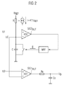
- FIG. 2 is such an analog divider represented by the logic circuits in accordance with FIG. 1 occurring inaccuracies are minimized.
- a first comparator KO1 a sawtooth signal whose peak value corresponds to the value of a first input voltage U1, compared with the value of a second input voltage U2.
- the quotient thus corresponds to the mean value of the pulse width modulated signal applied as output voltage U D.
- the accuracy of the division depends on the one hand on the quality of the sawtooth signal and on the other hand on the response of the first comparator KO1.
- the charging circuit comprises by way of example a voltage source which supplies a constant reference voltage U REF and is connected via a resistor R to the negative terminal of a second comparator KO2.
- the capacitor C is a switching element connected in parallel as part of the discharge circuit, wherein the mono-flip-flop MFF to which the second comparison signal SIG2 OUT is supplied at each high-low transition a turn-on with a pulse duration t FF greater than Discharge time of the capacitor C supplies.
- t ⁇ 2 U ⁇ 2 * C / K * U REF
- the duty cycle of the pulse width modulated signal at the output of the first capacitor KO1 is thus independent of the electrical properties of the capacitor C and the resistor R or the coefficient K.
- t ⁇ 2 / t ⁇ 1 U ⁇ 2 * C / K * U REF / ( U ⁇ 1 * C / K * U REF )
- t ⁇ 2 / t ⁇ 1 U ⁇ 2 / U ⁇ 1
- a smoothing member is arranged, consisting of a smoothing resistor R O and a smoothing capacitor C O , wherein the smoothing capacitor C O is connected to a reference potential of the voltages.
- this smoothing element is then applied as an average value of the first comparison signal SIG1 OUT an output voltage U D as a quotient of the division.
- FIG. 3 shows the waveforms in the operation of the circuit according to FIG. 2 , where four diagrams with a constant time axis are shown as abscissa.
- the voltage UC at the capacitor C and the second input voltage U2 over the time t are shown.
- the voltage UC at the capacitor C follows a sawtooth signal having a peak value equal to the value of the first input voltage U1.
- the intersections between the two voltage curves mark the high-low transitions of the first comparison signal SIG1 OUT at the output of the first comparator KO1, shown in the fourth diagram.
- the output voltage U D at the output of the smoothing element is shown as the mean value of the first comparison signal SIG1 OUT .
- the second diagram shows the course of the second comparison signal SIG2 OUT at the output of the second comparator KO2 over the time t.
- the high-low transition takes place as soon as the voltage UC at the capacitor C is the value of the first Input voltage U1 reached.
- Each high-low transition triggers a switch-on pulse of the switching element of the discharge circuit by means of a mono-flip-flop MFF, so that the voltage UC at the capacitor C drops abruptly and the second comparison signal SIG2 OUT again assumes the high-signal state.
- the duration t FF of each switch-on pulse must be at least as long as the discharge duration of the capacitor C.
- the pulse duration t FF must not significantly exceed the discharge duration, because the short-term occurrence of the capacitor voltage UC constant portions of the sawtooth signal then cause inaccuracies in the quotient formation. The occurring error is greater, the greater the frequency.
- the circuit shown has the disadvantage that the frequency of the sawtooth signal increases with decreasing input voltage U1. Over a constant observation period, more constant sections of the sawtooth signal thus occur.
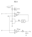
- the auxiliary voltage of the charging circuit is set in a fixed ratio to the first input voltage U1.
- a corresponding circuit arrangement is in FIG. 4 shown. Except for the formation of the auxiliary voltage, the arrangement corresponds to in FIG. 2 shown.
- a triangular generator is arranged in the circuit instead of a sawtooth generator.
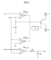
- FIG. 5 a corresponding circuit arrangement is shown.
- the negative input of the first comparator KO1 is supplied with a triangular signal whose peak value corresponds to the value of the first input voltage U1.
- This triangular signal is formed by means of a second comparator KO2, to whose positive input the first input voltage U1 and to whose negative input a capacitor C is connected.
- the negative input of the second comparator KO2 is connected to the negative input of the first comparator KO1.
- the capacitor C is cyclically charged and discharged by means of a charge and discharge circuit in such a way that a triangular signal is given.
- the charging and discharging circuit in this case comprises a switching element which turns on the capacitor C alternately to a current source with a charging current + i1 and to a current sink with a discharge current -i2.
- This switching element is controlled by means of a latch LA, also called a delay flip-flop, whose first input to the output of the second comparator KO2 and whose second input is connected to the output of a third comparator KO3.
- the third comparator KO3 is connected to the negative input to a reference potential of the voltages and the positive input is connected to the negative inputs of the two other comparators KO1, KO2.
- the first input signal of the latch LA has a high-low transition when the voltage UC across the capacitor C reaches the value of the first input voltage U1.
- a high-low transition of the second input signal of the latch LA occurs when the voltage across the capacitor C reaches the value of the reference potential.
- FIG. 6 is also shown a circuit arrangement with triangular generator, in which case instead of the current sources and the current sink, a positive and a negative voltage source + U REF 1, -U REF 2 are provided.
- driven latch LA switches the voltage sources + U REF 1, -U REF 2 alternately to the input of an integrator INT, which is formed, for example, as with a capacitor C and a resistor R connected operational amplifier.
- the output is then again the desired triangular signal U triangle , which is supplied to the negative input of the first comparator KO1.
- the corresponding diagrams of the signal sequences in an analog divider with triangular generator are in FIG. 7 shown.
- Six diagrams with a constant time axis are arranged as abscissa.
- the first diagram shows the profile of the voltage UC at the capacitor C, the first input voltage U1 and the second input voltage U2 over the time t.
- the capacitor voltage UC follows a triangular signal with a cyclical sequence of a rising ramp from the value of the reference potential to the value of the first input voltage U1 during a first time interval t S and a falling ramp from the value of the first input voltage U1 to the value of the reference potential during a second time period t f .
- the two input signals of the latch LA assume the low-signal states only for the duration of the response times of the corresponding comparators KO2, KO3 and then immediately return to the high-signal state, because immediately after the response of a comparator KO2, KO3 a switching of the Switching element by means of Latch LA done.
- the curves of the first and the second input signal over the time t are in the second and third diagram of FIG. 7 shown.
- the fourth diagram shows the turn-on times of the current source to the capacitor C over the time t.
- the ON connection is effected by means of a switching element as soon as the second input of the latch LA is subjected to a high-low transition, with a positive charging current + i1 flowing into the capacitor C.
- the switch-off occurs OFF.
- the shutoff OFF from the power source is at the same time the connection ON to the current sink and a discharge current -i2 flows from the capacitor C to the current sink until the capacitor voltage UC has reached the value of the reference potential.
- the course of the turn-on times of the current sink to the capacitor C is shown in the fifth diagram.
- the triangular signal generated in this way is compared in the first comparator KO1 with the second input voltage U2.
- the first comparison signal SIG1 OUT at the output of the The first comparator KO1 is then again a pulse width modulated signal whose duty cycle corresponds to the quotient of the division of the second input voltage U2 by the first input voltage U1:
- U ⁇ 2 / U ⁇ 1 t ⁇ 2 / t ⁇ 1 with t2 as the duration of the high-signal state
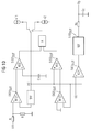
- FIG. 9 An exemplary embodiment of the invention is in FIG. 9 shown.
- the two comparators KO2, KO3 of a triangular generator are preceded by two regulators REG1, REG2.
- the first regulator REG1 is supplied with the first input voltage U1 as the setpoint signal. This setpoint signal is by means of the first controller REG1 with the Actual values of the upper peak values of the triangular signal compared.
- the triangular signal formed as a capacitor voltage UC is supplied to an input of the first regulator REG1.
- the first regulator REG1 forms from the input variables a control signal SIG4 OUT , which is supplied to the second comparator KO2 for comparison with the triangular signal.
- the actuating signal SIG4 OUT is predetermined such that the actual peak values of the triangular signal of the first input voltage U1 are readjusted.
- the second regulator REG2 is supplied with the triangular signal.
- the second regulator REG2 compares the lower actual peak values of the triangular signal with a reference potential.
- the control signal SIG5 OUT of the second regulator REG2 is supplied to the third comparator KO3 for comparison with the triangular signal.
- the lower peak values of the triangular signal are readjusted to the value of the reference potential.
- comparators generally have a higher slew rate than operational amplifiers. Therefore, regulators REG1, REG2 with correspondingly high slew rates must be provided.
- the mean value of the triangular signal is formed by means of a low-pass filter TPF, which is connected upstream of the first regulator REG1.
- Half the value of the first input voltage U1 is formed by means of a voltage divider.
- the voltage divider comprises two high-impedance resistors R, which are arranged in series between the first input voltage U1 and the reference potential, wherein a connection point between the resistors R and an input of the first Regulator REG1 is connected. Otherwise corresponds to in FIG. 10 illustrated arrangement of in FIG. 9 shown.
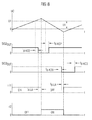
- FIG. 11 shows the waveform during operation of an analog divider according to the invention.
- the triangular signal is shown as a capacitor voltage UC, superimposed by the curves of the reference potential 0, the first input voltage U1, the second input voltage U2 and the control signals SIG4 OUT , SIG5 OUT of the two regulators REG1, REG2.
- the first regulator REG1 forms a control signal SIG4 OUT whose profile is below the curve of the input voltage U1.
- the difference to the input voltage U1 is so great that the response times td-KO2 , td -LA of the second comparator KO2 and the latch LA are compensated and the rising ramp of the triangular signal ends precisely upon reaching the value of the input voltage U1.
- the second regulator REG2 forms a control signal SIG4 OUT whose profile is above the course of the reference potential 0.
- the difference to the reference potential 0 is again so great that the response times td-KO3 , td -LA of the third comparator KO3 and the latch LA are compensated and the falling ramp of the triangular signal terminates precisely when the reference potential is reached.
- a further increase in accuracy is achieved by the stabilization of the two signal states at the output of the first comparator KO1.
- a switchable reference unit REF is connected downstream of the first comparator KO1. At the output of the reference unit REF is then applied to a referenced signal SIG6 OUT that changes according to the first comparison signal SIG1 OUT at the output of the first comparator KO1 between a referenced high value + U REF-S and a referenced low value.
Landscapes
- Engineering & Computer Science (AREA)
- Physics & Mathematics (AREA)
- Mathematical Physics (AREA)
- Theoretical Computer Science (AREA)
- Power Engineering (AREA)
- Software Systems (AREA)
- Computer Hardware Design (AREA)
- General Physics & Mathematics (AREA)
- Dc-Dc Converters (AREA)
- Inverter Devices (AREA)
- Analogue/Digital Conversion (AREA)
- Pulse Circuits (AREA)
Applications Claiming Priority (1)
| Application Number | Priority Date | Filing Date | Title |
|---|---|---|---|
| AT9432007A AT505446B1 (de) | 2007-06-19 | 2007-06-19 | Analog dividierer |
Publications (3)
| Publication Number | Publication Date |
|---|---|
| EP2012250A2 true EP2012250A2 (fr) | 2009-01-07 |
| EP2012250A3 EP2012250A3 (fr) | 2011-10-12 |
| EP2012250B1 EP2012250B1 (fr) | 2013-11-13 |
Family
ID=39767140
Family Applications (1)
| Application Number | Title | Priority Date | Filing Date |
|---|---|---|---|
| EP20080103649 Not-in-force EP2012250B1 (fr) | 2007-06-19 | 2008-04-22 | Diviseur analogique |
Country Status (2)
| Country | Link |
|---|---|
| EP (1) | EP2012250B1 (fr) |
| AT (1) | AT505446B1 (fr) |
Citations (1)
| Publication number | Priority date | Publication date | Assignee | Title |
|---|---|---|---|---|
| JP2005157721A (ja) | 2003-11-26 | 2005-06-16 | Yokogawa Electric Corp | アナログ除算器 |
Family Cites Families (7)
| Publication number | Priority date | Publication date | Assignee | Title |
|---|---|---|---|---|
| US3024999A (en) * | 1959-02-11 | 1962-03-13 | Jr William J Heacock | Electronic divider |
| US3278737A (en) * | 1962-08-03 | 1966-10-11 | Gulton Ind Inc | Quotient circuit |
| US3976894A (en) * | 1975-02-03 | 1976-08-24 | Raytheon Company | Analog divider circuitry |
| DE3037416A1 (de) * | 1980-10-03 | 1982-05-19 | Vdo Adolf Schindling Ag, 6000 Frankfurt | Elektronischer dividierer |
| US6765519B2 (en) * | 2002-12-23 | 2004-07-20 | Agilent Technologies, Inc. | System and method for designing and using analog circuits operating in the modulation domain |
| DE202004019553U1 (de) * | 2004-12-18 | 2005-03-03 | Lerner, Zinoviy, Dipl.-Ing. | Multiplizierer-Dividierer |
| DE102005030599A1 (de) * | 2005-06-30 | 2007-01-11 | Siemens Ag Österreich | Steuerungsverfahren für zweistufige Konverter |
-
2007
- 2007-06-19 AT AT9432007A patent/AT505446B1/de not_active IP Right Cessation
-
2008
- 2008-04-22 EP EP20080103649 patent/EP2012250B1/fr not_active Not-in-force
Patent Citations (1)
| Publication number | Priority date | Publication date | Assignee | Title |
|---|---|---|---|---|
| JP2005157721A (ja) | 2003-11-26 | 2005-06-16 | Yokogawa Electric Corp | アナログ除算器 |
Also Published As
| Publication number | Publication date |
|---|---|
| EP2012250B1 (fr) | 2013-11-13 |
| AT505446A1 (de) | 2009-01-15 |
| AT505446B1 (de) | 2009-08-15 |
| EP2012250A3 (fr) | 2011-10-12 |
Similar Documents
| Publication | Publication Date | Title |
|---|---|---|
| EP3701274B1 (fr) | Procédé pour faire fonctionner un capteur de batterie et capteur de batterie | |
| DE19920306B4 (de) | Schaltungsvorrichtung zum Regeln des Stroms durch eine induktive Last | |
| DE112009001360B4 (de) | Massenspektrometer mit Spannungsstabilisierung mittels Leerbetrieb | |
| EP0415490B1 (fr) | Disposition de circuit pour l'alimentation d'une charge | |
| EP0149277B1 (fr) | Oscillateur RC à intégration monolithique | |
| DE102006011448B4 (de) | Schaltungsanordnung und Verfahren zum Bereitstellen eines Taktsignals mit einem einstellbaren Tastverhältnis | |
| DE102013219173B4 (de) | Spannungsversorgung für elektrische Fokussierung von Elektronenstrahlen | |
| DE10223996A1 (de) | Referenzspannungsschaltung und Verfahren zum Erzeugen einer Referenzspannung | |
| EP2582044B1 (fr) | Mesure du courant de sortie d'un circuit d'amplification | |
| DE2249082C3 (de) | Dreieckspannungsgenerator | |
| EP2012250B1 (fr) | Diviseur analogique | |
| DE102008018811A1 (de) | Verfahren zur Bestimmung des Nulldurchganges des Motorstromes in einem pulsweitengeregelten Motor | |
| CH669048A5 (de) | Verfahren zur messung des verhaeltnisses einer messgroessenabhaengigen kapazitaet zu einer referenzkapazitaet und einrichtung zur durchfuehrung des verfahrens. | |
| EP1949114B1 (fr) | Procede pour mesurer le courant d'un moteur | |
| EP3836383A1 (fr) | Procédé d'identification d'une inductance d'un filtre de réseau d'un onduleur | |
| EP1208645A1 (fr) | Circuit pour produire des impulsions carrees | |
| AT401985B (de) | Analog-digital-umsetzer | |
| EP2629419B1 (fr) | Dispositif destiné à la production d'impulsions électriques courtes | |
| EP0071608B1 (fr) | Generateur de tension en dent de scie | |
| WO2002007313A1 (fr) | Procede et dispositif d'evaluation de la puissance d'un circuit d'attaque | |
| DE102016225044A1 (de) | Linearisierungsschaltung und Verfahren zum Linearisieren eines Messsignals | |
| DE2543777A1 (de) | Saegezahn-spannungsgenerator | |
| DE10301501A1 (de) | Schaltungsanordnung und Verfahren zur Erzeugung eines Pulsweiten-modulierten Signals | |
| DE202012012781U1 (de) | Integrierender A/D-Wandler | |
| DE102013225140A1 (de) | Gleichspannungswandler und dessen Verwendung |
Legal Events
| Date | Code | Title | Description |
|---|---|---|---|
| PUAI | Public reference made under article 153(3) epc to a published international application that has entered the european phase |
Free format text: ORIGINAL CODE: 0009012 |
|
| AK | Designated contracting states |
Kind code of ref document: A2 Designated state(s): AT BE BG CH CY CZ DE DK EE ES FI FR GB GR HR HU IE IS IT LI LT LU LV MC MT NL NO PL PT RO SE SI SK TR |
|
| AX | Request for extension of the european patent |
Extension state: AL BA MK RS |
|
| RAP1 | Party data changed (applicant data changed or rights of an application transferred) |
Owner name: SIEMENS AKTIENGESELLSCHAFT |
|
| PUAL | Search report despatched |
Free format text: ORIGINAL CODE: 0009013 |
|
| AK | Designated contracting states |
Kind code of ref document: A3 Designated state(s): AT BE BG CH CY CZ DE DK EE ES FI FR GB GR HR HU IE IS IT LI LT LU LV MC MT NL NO PL PT RO SE SI SK TR |
|
| AX | Request for extension of the european patent |
Extension state: AL BA MK RS |
|
| RIC1 | Information provided on ipc code assigned before grant |
Ipc: G06G 7/161 20060101ALI20110905BHEP Ipc: G06G 7/16 20060101AFI20110905BHEP |
|
| 17P | Request for examination filed |
Effective date: 20120412 |
|
| AKX | Designation fees paid |
Designated state(s): AT BE BG CH CY CZ DE DK EE ES FI FR GB GR HR HU IE IS IT LI LT LU LV MC MT NL NO PL PT RO SE SI SK TR |
|
| 17Q | First examination report despatched |
Effective date: 20120614 |
|
| RAP1 | Party data changed (applicant data changed or rights of an application transferred) |
Owner name: SIEMENS AKTIENGESELLSCHAFT |
|
| GRAP | Despatch of communication of intention to grant a patent |
Free format text: ORIGINAL CODE: EPIDOSNIGR1 |
|
| INTG | Intention to grant announced |
Effective date: 20130607 |
|
| GRAS | Grant fee paid |
Free format text: ORIGINAL CODE: EPIDOSNIGR3 |
|
| GRAA | (expected) grant |
Free format text: ORIGINAL CODE: 0009210 |
|
| AK | Designated contracting states |
Kind code of ref document: B1 Designated state(s): AT BE BG CH CY CZ DE DK EE ES FI FR GB GR HR HU IE IS IT LI LT LU LV MC MT NL NO PL PT RO SE SI SK TR |
|
| REG | Reference to a national code |
Ref country code: GB Ref legal event code: FG4D Free format text: NOT ENGLISH |
|
| REG | Reference to a national code |
Ref country code: CH Ref legal event code: EP |
|
| REG | Reference to a national code |
Ref country code: AT Ref legal event code: REF Ref document number: 640836 Country of ref document: AT Kind code of ref document: T Effective date: 20131215 |
|
| REG | Reference to a national code |
Ref country code: IE Ref legal event code: FG4D Free format text: LANGUAGE OF EP DOCUMENT: GERMAN |
|
| REG | Reference to a national code |
Ref country code: DE Ref legal event code: R096 Ref document number: 502008010944 Country of ref document: DE Effective date: 20140109 |
|
| REG | Reference to a national code |
Ref country code: NL Ref legal event code: VDEP Effective date: 20131113 |
|
| REG | Reference to a national code |
Ref country code: LT Ref legal event code: MG4D |
|
| PG25 | Lapsed in a contracting state [announced via postgrant information from national office to epo] |
Ref country code: FI Free format text: LAPSE BECAUSE OF FAILURE TO SUBMIT A TRANSLATION OF THE DESCRIPTION OR TO PAY THE FEE WITHIN THE PRESCRIBED TIME-LIMIT Effective date: 20131113 Ref country code: IS Free format text: LAPSE BECAUSE OF FAILURE TO SUBMIT A TRANSLATION OF THE DESCRIPTION OR TO PAY THE FEE WITHIN THE PRESCRIBED TIME-LIMIT Effective date: 20140313 Ref country code: NL Free format text: LAPSE BECAUSE OF FAILURE TO SUBMIT A TRANSLATION OF THE DESCRIPTION OR TO PAY THE FEE WITHIN THE PRESCRIBED TIME-LIMIT Effective date: 20131113 Ref country code: LT Free format text: LAPSE BECAUSE OF FAILURE TO SUBMIT A TRANSLATION OF THE DESCRIPTION OR TO PAY THE FEE WITHIN THE PRESCRIBED TIME-LIMIT Effective date: 20131113 Ref country code: HR Free format text: LAPSE BECAUSE OF FAILURE TO SUBMIT A TRANSLATION OF THE DESCRIPTION OR TO PAY THE FEE WITHIN THE PRESCRIBED TIME-LIMIT Effective date: 20131113 Ref country code: NO Free format text: LAPSE BECAUSE OF FAILURE TO SUBMIT A TRANSLATION OF THE DESCRIPTION OR TO PAY THE FEE WITHIN THE PRESCRIBED TIME-LIMIT Effective date: 20140213 Ref country code: SE Free format text: LAPSE BECAUSE OF FAILURE TO SUBMIT A TRANSLATION OF THE DESCRIPTION OR TO PAY THE FEE WITHIN THE PRESCRIBED TIME-LIMIT Effective date: 20131113 |
|
| PG25 | Lapsed in a contracting state [announced via postgrant information from national office to epo] |
Ref country code: CY Free format text: LAPSE BECAUSE OF FAILURE TO SUBMIT A TRANSLATION OF THE DESCRIPTION OR TO PAY THE FEE WITHIN THE PRESCRIBED TIME-LIMIT Effective date: 20131113 Ref country code: LV Free format text: LAPSE BECAUSE OF FAILURE TO SUBMIT A TRANSLATION OF THE DESCRIPTION OR TO PAY THE FEE WITHIN THE PRESCRIBED TIME-LIMIT Effective date: 20131113 Ref country code: ES Free format text: LAPSE BECAUSE OF FAILURE TO SUBMIT A TRANSLATION OF THE DESCRIPTION OR TO PAY THE FEE WITHIN THE PRESCRIBED TIME-LIMIT Effective date: 20131113 |
|
| PG25 | Lapsed in a contracting state [announced via postgrant information from national office to epo] |
Ref country code: PT Free format text: LAPSE BECAUSE OF FAILURE TO SUBMIT A TRANSLATION OF THE DESCRIPTION OR TO PAY THE FEE WITHIN THE PRESCRIBED TIME-LIMIT Effective date: 20140313 |
|
| PG25 | Lapsed in a contracting state [announced via postgrant information from national office to epo] |
Ref country code: EE Free format text: LAPSE BECAUSE OF FAILURE TO SUBMIT A TRANSLATION OF THE DESCRIPTION OR TO PAY THE FEE WITHIN THE PRESCRIBED TIME-LIMIT Effective date: 20131113 |
|
| REG | Reference to a national code |
Ref country code: DE Ref legal event code: R097 Ref document number: 502008010944 Country of ref document: DE |
|
| PG25 | Lapsed in a contracting state [announced via postgrant information from national office to epo] |
Ref country code: RO Free format text: LAPSE BECAUSE OF FAILURE TO SUBMIT A TRANSLATION OF THE DESCRIPTION OR TO PAY THE FEE WITHIN THE PRESCRIBED TIME-LIMIT Effective date: 20131113 Ref country code: SK Free format text: LAPSE BECAUSE OF FAILURE TO SUBMIT A TRANSLATION OF THE DESCRIPTION OR TO PAY THE FEE WITHIN THE PRESCRIBED TIME-LIMIT Effective date: 20131113 Ref country code: CZ Free format text: LAPSE BECAUSE OF FAILURE TO SUBMIT A TRANSLATION OF THE DESCRIPTION OR TO PAY THE FEE WITHIN THE PRESCRIBED TIME-LIMIT Effective date: 20131113 Ref country code: PL Free format text: LAPSE BECAUSE OF FAILURE TO SUBMIT A TRANSLATION OF THE DESCRIPTION OR TO PAY THE FEE WITHIN THE PRESCRIBED TIME-LIMIT Effective date: 20131113 |
|
| PLBE | No opposition filed within time limit |
Free format text: ORIGINAL CODE: 0009261 |
|
| STAA | Information on the status of an ep patent application or granted ep patent |
Free format text: STATUS: NO OPPOSITION FILED WITHIN TIME LIMIT |
|
| PG25 | Lapsed in a contracting state [announced via postgrant information from national office to epo] |
Ref country code: DK Free format text: LAPSE BECAUSE OF FAILURE TO SUBMIT A TRANSLATION OF THE DESCRIPTION OR TO PAY THE FEE WITHIN THE PRESCRIBED TIME-LIMIT Effective date: 20131113 |
|
| 26N | No opposition filed |
Effective date: 20140814 |
|
| REG | Reference to a national code |
Ref country code: DE Ref legal event code: R097 Ref document number: 502008010944 Country of ref document: DE Effective date: 20140814 |
|
| PG25 | Lapsed in a contracting state [announced via postgrant information from national office to epo] |
Ref country code: LU Free format text: LAPSE BECAUSE OF FAILURE TO SUBMIT A TRANSLATION OF THE DESCRIPTION OR TO PAY THE FEE WITHIN THE PRESCRIBED TIME-LIMIT Effective date: 20140422 Ref country code: MC Free format text: LAPSE BECAUSE OF FAILURE TO SUBMIT A TRANSLATION OF THE DESCRIPTION OR TO PAY THE FEE WITHIN THE PRESCRIBED TIME-LIMIT Effective date: 20131113 |
|
| REG | Reference to a national code |
Ref country code: CH Ref legal event code: PL |
|
| GBPC | Gb: european patent ceased through non-payment of renewal fee |
Effective date: 20140422 |
|
| REG | Reference to a national code |
Ref country code: FR Ref legal event code: ST Effective date: 20141231 |
|
| REG | Reference to a national code |
Ref country code: IE Ref legal event code: MM4A |
|
| PG25 | Lapsed in a contracting state [announced via postgrant information from national office to epo] |
Ref country code: LI Free format text: LAPSE BECAUSE OF NON-PAYMENT OF DUE FEES Effective date: 20140430 Ref country code: GB Free format text: LAPSE BECAUSE OF NON-PAYMENT OF DUE FEES Effective date: 20140422 Ref country code: CH Free format text: LAPSE BECAUSE OF NON-PAYMENT OF DUE FEES Effective date: 20140430 |
|
| PG25 | Lapsed in a contracting state [announced via postgrant information from national office to epo] |
Ref country code: SI Free format text: LAPSE BECAUSE OF FAILURE TO SUBMIT A TRANSLATION OF THE DESCRIPTION OR TO PAY THE FEE WITHIN THE PRESCRIBED TIME-LIMIT Effective date: 20131113 Ref country code: FR Free format text: LAPSE BECAUSE OF NON-PAYMENT OF DUE FEES Effective date: 20140430 |
|
| PG25 | Lapsed in a contracting state [announced via postgrant information from national office to epo] |
Ref country code: IT Free format text: LAPSE BECAUSE OF FAILURE TO SUBMIT A TRANSLATION OF THE DESCRIPTION OR TO PAY THE FEE WITHIN THE PRESCRIBED TIME-LIMIT Effective date: 20131113 |
|
| PG25 | Lapsed in a contracting state [announced via postgrant information from national office to epo] |
Ref country code: IE Free format text: LAPSE BECAUSE OF NON-PAYMENT OF DUE FEES Effective date: 20140422 |
|
| REG | Reference to a national code |
Ref country code: AT Ref legal event code: MM01 Ref document number: 640836 Country of ref document: AT Kind code of ref document: T Effective date: 20140422 |
|
| PG25 | Lapsed in a contracting state [announced via postgrant information from national office to epo] |
Ref country code: AT Free format text: LAPSE BECAUSE OF NON-PAYMENT OF DUE FEES Effective date: 20140422 |
|
| PG25 | Lapsed in a contracting state [announced via postgrant information from national office to epo] |
Ref country code: MT Free format text: LAPSE BECAUSE OF FAILURE TO SUBMIT A TRANSLATION OF THE DESCRIPTION OR TO PAY THE FEE WITHIN THE PRESCRIBED TIME-LIMIT Effective date: 20131113 |
|
| PG25 | Lapsed in a contracting state [announced via postgrant information from national office to epo] |
Ref country code: BG Free format text: LAPSE BECAUSE OF FAILURE TO SUBMIT A TRANSLATION OF THE DESCRIPTION OR TO PAY THE FEE WITHIN THE PRESCRIBED TIME-LIMIT Effective date: 20131113 |
|
| PG25 | Lapsed in a contracting state [announced via postgrant information from national office to epo] |
Ref country code: GR Free format text: LAPSE BECAUSE OF FAILURE TO SUBMIT A TRANSLATION OF THE DESCRIPTION OR TO PAY THE FEE WITHIN THE PRESCRIBED TIME-LIMIT Effective date: 20140214 |
|
| PG25 | Lapsed in a contracting state [announced via postgrant information from national office to epo] |
Ref country code: HU Free format text: LAPSE BECAUSE OF FAILURE TO SUBMIT A TRANSLATION OF THE DESCRIPTION OR TO PAY THE FEE WITHIN THE PRESCRIBED TIME-LIMIT; INVALID AB INITIO Effective date: 20080422 Ref country code: BE Free format text: LAPSE BECAUSE OF FAILURE TO SUBMIT A TRANSLATION OF THE DESCRIPTION OR TO PAY THE FEE WITHIN THE PRESCRIBED TIME-LIMIT Effective date: 20140430 Ref country code: TR Free format text: LAPSE BECAUSE OF FAILURE TO SUBMIT A TRANSLATION OF THE DESCRIPTION OR TO PAY THE FEE WITHIN THE PRESCRIBED TIME-LIMIT Effective date: 20131113 |
|
| PGFP | Annual fee paid to national office [announced via postgrant information from national office to epo] |
Ref country code: DE Payment date: 20200619 Year of fee payment: 13 |
|
| REG | Reference to a national code |
Ref country code: DE Ref legal event code: R119 Ref document number: 502008010944 Country of ref document: DE |
|
| PG25 | Lapsed in a contracting state [announced via postgrant information from national office to epo] |
Ref country code: DE Free format text: LAPSE BECAUSE OF NON-PAYMENT OF DUE FEES Effective date: 20211103 |