EP2011219B1 - Methods and apparatus for switching regulator control - Google Patents
Methods and apparatus for switching regulator control Download PDFInfo
- Publication number
- EP2011219B1 EP2011219B1 EP07753499.8A EP07753499A EP2011219B1 EP 2011219 B1 EP2011219 B1 EP 2011219B1 EP 07753499 A EP07753499 A EP 07753499A EP 2011219 B1 EP2011219 B1 EP 2011219B1
- Authority
- EP
- European Patent Office
- Prior art keywords
- current
- coupled
- sense
- load
- coupling
- Prior art date
- Legal status (The legal status is an assumption and is not a legal conclusion. Google has not performed a legal analysis and makes no representation as to the accuracy of the status listed.)
- Not-in-force
Links
Images


Classifications
-
- H—ELECTRICITY
- H02—GENERATION; CONVERSION OR DISTRIBUTION OF ELECTRIC POWER
- H02M—APPARATUS FOR CONVERSION BETWEEN AC AND AC, BETWEEN AC AND DC, OR BETWEEN DC AND DC, AND FOR USE WITH MAINS OR SIMILAR POWER SUPPLY SYSTEMS; CONVERSION OF DC OR AC INPUT POWER INTO SURGE OUTPUT POWER; CONTROL OR REGULATION THEREOF
- H02M3/00—Conversion of DC power input into DC power output
- H02M3/02—Conversion of DC power input into DC power output without intermediate conversion into AC
- H02M3/04—Conversion of DC power input into DC power output without intermediate conversion into AC by static converters
- H02M3/10—Conversion of DC power input into DC power output without intermediate conversion into AC by static converters using discharge tubes with control electrode or semiconductor devices with control electrode
- H02M3/145—Conversion of DC power input into DC power output without intermediate conversion into AC by static converters using discharge tubes with control electrode or semiconductor devices with control electrode using devices of a triode or transistor type requiring continuous application of a control signal
- H02M3/155—Conversion of DC power input into DC power output without intermediate conversion into AC by static converters using discharge tubes with control electrode or semiconductor devices with control electrode using devices of a triode or transistor type requiring continuous application of a control signal using semiconductor devices only
- H02M3/156—Conversion of DC power input into DC power output without intermediate conversion into AC by static converters using discharge tubes with control electrode or semiconductor devices with control electrode using devices of a triode or transistor type requiring continuous application of a control signal using semiconductor devices only with automatic control of output voltage or current, e.g. switching regulators
-
- H—ELECTRICITY
- H05—ELECTRIC TECHNIQUES NOT OTHERWISE PROVIDED FOR
- H05B—ELECTRIC HEATING; ELECTRIC LIGHT SOURCES NOT OTHERWISE PROVIDED FOR; CIRCUIT ARRANGEMENTS FOR ELECTRIC LIGHT SOURCES, IN GENERAL
- H05B45/00—Circuit arrangements for operating light-emitting diodes [LED]
- H05B45/10—Controlling the intensity of the light
-
- H—ELECTRICITY
- H05—ELECTRIC TECHNIQUES NOT OTHERWISE PROVIDED FOR
- H05B—ELECTRIC HEATING; ELECTRIC LIGHT SOURCES NOT OTHERWISE PROVIDED FOR; CIRCUIT ARRANGEMENTS FOR ELECTRIC LIGHT SOURCES, IN GENERAL
- H05B45/00—Circuit arrangements for operating light-emitting diodes [LED]
- H05B45/30—Driver circuits
- H05B45/37—Converter circuits
- H05B45/3725—Switched mode power supply [SMPS]
-
- H—ELECTRICITY
- H05—ELECTRIC TECHNIQUES NOT OTHERWISE PROVIDED FOR
- H05B—ELECTRIC HEATING; ELECTRIC LIGHT SOURCES NOT OTHERWISE PROVIDED FOR; CIRCUIT ARRANGEMENTS FOR ELECTRIC LIGHT SOURCES, IN GENERAL
- H05B45/00—Circuit arrangements for operating light-emitting diodes [LED]
- H05B45/30—Driver circuits
- H05B45/37—Converter circuits
- H05B45/3725—Switched mode power supply [SMPS]
- H05B45/38—Switched mode power supply [SMPS] using boost topology
-
- Y—GENERAL TAGGING OF NEW TECHNOLOGICAL DEVELOPMENTS; GENERAL TAGGING OF CROSS-SECTIONAL TECHNOLOGIES SPANNING OVER SEVERAL SECTIONS OF THE IPC; TECHNICAL SUBJECTS COVERED BY FORMER USPC CROSS-REFERENCE ART COLLECTIONS [XRACs] AND DIGESTS
- Y02—TECHNOLOGIES OR APPLICATIONS FOR MITIGATION OR ADAPTATION AGAINST CLIMATE CHANGE
- Y02B—CLIMATE CHANGE MITIGATION TECHNOLOGIES RELATED TO BUILDINGS, e.g. HOUSING, HOUSE APPLIANCES OR RELATED END-USER APPLICATIONS
- Y02B20/00—Energy efficient lighting technologies, e.g. halogen lamps or gas discharge lamps
- Y02B20/30—Semiconductor lamps, e.g. solid state lamps [SSL] light emitting diodes [LED] or organic LED [OLED]
Definitions
- converter devices can provide a regulated DC (direct current) output signal to energize a load.
- DC direct current
- Such converters have a wide range of applications.
- One such application is for energizing LEDs (light emitting diodes).
- load components such as capacitors, can interfere with the stability of a feedback compensation loop since the capacitor will introduce additional poles and zeroes. Particularly for high current applications, this can limit the size and type of capacitor that can be used and thereby limit the switching response of the circuit.
- the present invention provides a converter circuit having load current filtering that is independent of a regulation loop. With this arrangement, a load capacitor, for example, does not interfere with loop stability to allow greater flexibility in selecting the capacitor. While the present invention is primarily shown and described in conjunction with a converter to regulate current through a high current LED stack, it is understood that the invention is applicable to loads in general for which it is desirable to regulate current.
- a converter circuit in one aspect of the invention, includes switch current terminals to receive current information for current through a switching element, and output current terminals to receive current information for the sum of the current through the load and the output capacitance.
- An inner loop is coupled to the switch current terminals to control an average inductor current by a peak switch current on a cycle-by-cycle basis, and an outer loop is coupled to the output current terminals to compare the output current to a reference current and generate and error signal to set an average amount of energy required by the load.
- a circuit in another aspect of the invention, includes an LED stack, a capacitor coupled across the LED stack, and a first current sensing resistor coupled in series with the LED stack and capacitor to detect the instantaneous sum of the currents through the LED stack and the capacitor.
- the circuit further includes a blocking diode with the cathode coupled to the LED stack and capacitor and an inductor with the first end coupled to the anode of the blocking diode and the second end coupled to an input voltage signal.
- a switching element is coupled to the inductor and blocking diode anode, wherein the switching element controls the current through the first current sensing resistor.
- a second current sensing resistor is coupled to the switching element; and with a converter circuit to control the switching element, wherein the converter regulates to the current level monitored across the first current sensing resistor.
- the circuit can further include one or more of the following features: a sixth terminal to receive a modulation signal; a seventh terminal to receive a current level selection signal; and an outer loop coupled to the first and second terminals and an inner loop coupled to the third and fourth terminals.
- FIG. 1 shows an exemplary circuit 100 having a converter 102 driving an LED stack 104.
- the converter 102 receives an input voltage signal 106 to a voltage input terminal VIN and provides a gate drive signal 108 on an output terminal SG coupled to a switching device 110, such as a Field Effect Transistor (FET).
- An inductor 114 is coupled between the voltage input terminal VIN and the switching device 110 with a current limit sense resistor (RSS) 112 coupled between the switching device 110 and ground.
- a LED current sense resistor (RSL) 115 is coupled between the LED stack 104 and the voltage input terminal VIN.
- a load capacitor 116 is coupled across the LED stack 104.
- first and second pulse width modulation (PWM) inputs PWM0, PWM1 provide a mechanism to select a PWM dimming level for the LEDs 104.
- First and second current select inputs ISET0, ISET1 allow a current level to be selected, as described more fully below. In other embodiments, more and fewer modulation and/or current level inputs are provided to meet the needs of a particular application.
- First and second LED current input terminals LN, LP are coupled across the LED current sense resistor (RSL) 115 to provide LED current information to the converter.
- First and second switch current input terminals SP, SN are coupled across the sense resistor (RSS) 112 to provide switch current information.
- An LED voltage input terminal VA is coupled to an anode of the LED stack 104 to provide LED voltage information via a resistor network comprising first and second resistors R1, R2. This enables the output voltage to be limited to a predetermined level, such as 50V.
- Table 1 below shows an exemplary pinout scheme for the converter 102 of FIG. 1.
- the converter 102 which can be referred to as a buck-boost DC-DC converter in an exemplary embodiment, provides a programmable constant current output at up to 50V, for example, for driving high power LEDs 104 in series. Driving the LEDs 104 in series ensures identical currents and uniform brightness. For automotive applications, for example, optimum performance is achieved when driving between two and ten LEDs at currents up to 1 A. In one embodiment, a constant frequency, current mode control scheme is used to regulate the current through the LEDs 104.
- the LEDs 104 are so-called high current LEDs that can draw for example, a maximum of 1A. Such LEDs can be used for various applications, such as vehicle headlamps. With the high current levels, conventional converters may provide inadequate switching characteristics. Unlike known implementations, the inventive embodiments do not require complex compensation networks that are load dependent. While topologies with comparable response times maybe possible for PWM dimming, such topologies require the user to compensate for the output load pole and zero introduced by an output capacitor.
- the load capacitor 116 does not interfere with the stability of the compensation loop.
- the illustrated circuit 100 has one terminal of the current sense device (RSL) 115 on the node connecting the capacitor 116 and LED stack 104 together and the other current sense device terminal to the current return path.
- RSL current sense device
- the current sense device (RSL) 115 provides an unfiltered feedback signal that is proportional to the current being output by the switching stage 130, the average of which is equal to the load current.
- the output load and ripple filter capacitor 116 and equivalent series resistance (ESR) of the capacitor have no effect on the system stability therefore allowing the user greater flexibility in setting the load resistance and filter capacitance.
- the output current from the switching stage 130 is a square wave and a current through the LED stack 104 has some degree of ripple.
- the current across the sense resistor RSL is a square wave. Since the load capacitor 116 is coupled across the LED stack, 104, the open loop response of the circuit in the frequency domain (Laplace transform variable s) is K ⁇ RSL ⁇ Gm 1 sCc , where K is a constant, RSL is the resistance of the sense resistor, Cc is the capacitance of the capacitor Cc, and Gm is the transconductance of the amplifier 135.
- the amplifier 135 outputs a current error signal le corresponding to a voltage Vyacross the sense resistor RSL multiplied by a gain value Gm.
- Capacitor Cc represents the capacitance of the integrator stage of the feedback loop (see outer loop 250 and AE 256 of FIG. 3 below) with an error voltage signal Ve being provided to the switching stage 130.
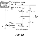
- FIG. 2B shows an alternative embodiment of the circuit of FIG. 2 , where like reference numbers indicate like elements.
- the circuit further includes a resistor R coupled across the series-coupled LED stack 104 and sense resistor RSL 115.
- a capacitor Copt is coupled across the sense resistor RSL to remove the high frequency edges from the voltage waveform across the sense resistor.
- the resistor R is intended to show that an extra load can be tapped from the switching stage 130. That is, current through the sense resistor RSL may not be equal to the current output of the switching element.
- High-powered LEDs can be run at average currents that are close to the absolute maximum current rating of the LEDs.
- the chromaticity of some LEDs is sensitive to the average current.
- the inventive method and apparatus embodiments allow the user to trade-off LED current ripple against load capacitor size and cost without being concerned about interfering with the loop stability. Minimizing the effect of the output load on the stability provides a more predictable and therefore higher GBW (gain-bandwidth product) to be set by the dominant pole, thus allowing faster system response to power supply disturbances and other unwanted transients.
- GBW gain-bandwidth product
- FIG. 3 shows an exemplary implementation of the converter 102 of FIG. 1 , where like reference numbers indicate like elements.
- the converter 102 includes an inner loop 200 that includes an amplifier (AS) 202, comparator (AC) 204, and RS bistable latch 208, to control the inductor current as measured through the switch 110 by the switch sense resistor (RSS) 112.
- the converter 102 further includes an outer loop 250 having an amplifier (AL) 252 and an integrating error amplifier (AE) 256 to control the average LED current by providing a set point reference for the inner loop 200.
- A amplifier
- AE integrating error amplifier
- the LED 104 current is measured by the LED sense resistor (RSL) 115 and compared to a reference current, which is selected by signals to the current level select inputs ISET0, ISET1, to produce an integrated error signal at the output of error amplifier AE 256.
- This error signal sets the average amount of energy required from the inductor 114 by the LEDs.
- the average inductor energy transferred to the LEDs is defined by the average inductor current as determined by the inner control loop 200.
- the LED current is determined by a combination of the LED sense resistor (RSL) 115, the LED current threshold voltage VIDL, and the current selection logic inputs ISET0 and ISET1 as set forth below in Table 2.
- Table 2 LED current settings: ISET1 ISET0 ILED 1 1 100% 1 0 90% 0 1 80% 0 0 70% where ILED at 100% is defined as: ILEDMAX VIDL / RSL This selection allows binning of the LED current to provide color matching between modules.
- the inner loop 200 establishes the average inductor current by controlling the peak switch current on a cycle-by-cycle basis. Since the relationship between peak current and average current is non-linear, depending on the duty cycle, the reference level for the peak switch current is modified by a slope generator 280, which reduces the peak switch current measurement by a small amount as the duty cycle increases. The slope generator 280 compensation also removes the instability inherent in a fixed frequency current control scheme.
- control loops 200, 250 work as follows: the switch 110 current sensed by the current sense resistor RSS is compared to the LED current error signal. As the LED current increases the output of the error amplifier (AE) 256 will decrease, reducing the peak switch current and thus the current delivered to the LEDs 104. As the LED current decreases the output of the error amplifier (AE) 256 increases, increasing the peak switch current and thus increasing the current delivered to the LEDs.
- the energy required in the inductor 114 may result in the inductor current dropping to zero for part of each cycle. This is known as discontinuous mode operation and will result in some low frequency ripple. The average LED current will however remain regulated down to zero.
- discontinuous mode when the inductor current drops to zero, the voltage at the drain of the external MOSFET will ring due to the resonant LC circuit formed by the inductor and the switch and diode capacitance. This ringing is low frequency and is not harmful.
- the frequency of the main oscillator is controlled by a single external resistor ROSC(k ⁇ ) between the OSC pin and the GND pin.
- the switch current is measured by the switch sense resistor RSS and the switch sense amplifier (AS) 202.
- the peak switch current will always be less than this, set by the control circuit, depending on the required load conditions.
- the LED brightness is determined by the current, it may be better to control the brightness by switching the current with a pulse width modulated signal. This allows the LED brightness to be set with little effect on the LED color.
- four discrete brightness levels are provided by an internal PWM generator and selected by the logic levels on the PWM0 and PWM1 inputs. Three of the brightness levels provide brightness binning while the third level is lower providing a level for dimming.
- An exemplary PWM brightness scheme is illustrated in Table 3 below.
- the inductor 114, switching MOSFET 110 and output capacitor 116 are the primary elements in the illustrative embodiment, the specification of the rectifying diode and sense resistors RSS, RSL should also be considered.
- the starting point for component selection is to define the maximum LED current, the voltage across the LEDs 104, and the input operating voltage range. This then allows the average inductor 114 current under worst case conditions to be calculated. The inductor 114 value is then selected based on the acceptable inductor ripple current. The amount of ripple current will then determine the maximum inductor current under worst-case conditions. From this current, the switch current sense resistor RSS can be calculated.
- the switch sense resistor RSS value should be chosen to maximize the differential signal seen by the sense amplifier (AS) 202.
- a logic-level n-channel MOSFET is used as the switch 110 for the DC-DC converter.
- the converter topology used is a buck-boost referenced to the positive supply. This means that the voltage at the drain of the MOSFET 110 will reach a voltage equal to the sum of the LED voltage and the supply voltage. Under load dump conditions up to 90V may be present on this node.
- the external MOSFET 110 should therefore be rated to greater than 100V.
- the peak switch current is defined by the maximum inductor current ILPK, however in most cases the MOSFET 110 will be chosen by selecting a low on-resistance, which usually results in a current rating of several times the required peak current. In addition to minimizing cost, the choice of MOSFET 110 should consider both the on-resistance and the total gate charge. The total gate charge will determine the average current required from the internal regulator and thus the power dissipation.
- the output capacitor 116 There are a variety of considerations when selecting the output capacitor 116.
- the capacitor value is limited by the maximum ripple voltage.
- the output capacitor 116 provides the LED current when the switch 110 is active. The capacitor 116 is then recharged each time the inductor 114 passes energy to the output.
- the ripple current on the output capacitor 116 will be equal to the peak inductor current.
- the value of the output capacitor 110 for the illustrated embodiment will typically be about 10 ⁇ F and it should be rated above the maximum voltage defined by the series output LEDs 104.
- the ripple current should be minimized to avoid exceeding the rated current level of the LEDs in the stack.
- the LEDs 104 may see a pure square wave well above the rated value as the circuit is first energized. While the load capacitor 116 filters the current to minimize peaks, the current sensing element RSL sees an unfiltered square wave so that the filtering is separate from the current regulation loop. Thus, the capacitor 116 does not factor into the regulation scheme described above.
- the converter limits current even during start up and does not need to wait for the capacitor 116 to charge.
- the LEDs 104 may see the maximum current that can be generated by the inductor 114 until current flows though the LED stack 104. The illustrated embodiment avoids current spikes during circuit start up.
- the inventive converter can be used in a variety of applications.
- the converter can energize a stack (e.g., two to ten) of high current (e.g., in the order of 1 A) LEDs.
- a stack e.g., two to ten
- high current e.g., in the order of 1 A
- the present embodiments use PWM or other modulation technique to set the brightness of the LEDs by controlling the duty cycle. That is, PWM provides a current level to generate the correct color for the diodes instead of simply 'turning down' the current. For example, at a PWM frequency of 200 Hz (5ms period) with a desired duty cycle of 90% results in 4.5 ms of on time and 0.5 ms of off time, preferably with a square waveform.
- Electrolytic capacitors have a limited ability to handle ripple currents due to a significant equivalent series resistance (ESR) component. Switching current into the electrolytic capacitor can result in unacceptable heating. For high current applications, such as 1A LEDs, this can limit the use of electrolytic capacitors in conventional implementations. While ceramic capacitors can better handle ripple currents due to less heating than electrolytic capacitors, ceramic capacitors are available at limited capacitance values, i.e., in the order of 10 ⁇ F. The inventive converter eliminates this capacitor ripple current tradeoff required in conventional implementations.
- ESR equivalent series resistance
Landscapes
- Engineering & Computer Science (AREA)
- Power Engineering (AREA)
- Dc-Dc Converters (AREA)
- Circuit Arrangement For Electric Light Sources In General (AREA)
Description
- As is known in the art, converter devices can provide a regulated DC (direct current) output signal to energize a load. Such converters have a wide range of applications. One such application is for energizing LEDs (light emitting diodes). In known configurations, load components, such as capacitors, can interfere with the stability of a feedback compensation loop since the capacitor will introduce additional poles and zeroes. Particularly for high current applications, this can limit the size and type of capacitor that can be used and thereby limit the switching response of the circuit.
-
-
-
- The present invention provides a converter circuit having load current filtering that is independent of a regulation loop. With this arrangement, a load capacitor, for example, does not interfere with loop stability to allow greater flexibility in selecting the capacitor. While the present invention is primarily shown and described in conjunction with a converter to regulate current through a high current LED stack, it is understood that the invention is applicable to loads in general for which it is desirable to regulate current.
- In one aspect of the invention, a converter circuit includes switch current terminals to receive current information for current through a switching element, and output current terminals to receive current information for the sum of the current through the load and the output capacitance. An inner loop is coupled to the switch current terminals to control an average inductor current by a peak switch current on a cycle-by-cycle basis, and an outer loop is coupled to the output current terminals to compare the output current to a reference current and generate and error signal to set an average amount of energy required by the load.
- In another aspect of the invention, a circuit includes an LED stack, a capacitor coupled across the LED stack, and a first current sensing resistor coupled in series with the LED stack and capacitor to detect the instantaneous sum of the currents through the LED stack and the capacitor. The circuit further includes a blocking diode with the cathode coupled to the LED stack and capacitor and an inductor with the first end coupled to the anode of the blocking diode and the second end coupled to an input voltage signal. A switching element is coupled to the inductor and blocking diode anode, wherein the switching element controls the current through the first current sensing resistor. A second current sensing resistor is coupled to the switching element; and with a converter circuit to control the switching element, wherein the converter regulates to the current level monitored across the first current sensing resistor.
- The circuit can further include one or more of the following features: a sixth terminal to receive a modulation signal; a seventh terminal to receive a current level selection signal; and an outer loop coupled to the first and second terminals and an inner loop coupled to the third and fourth terminals.
- The exemplary embodiments contained herein will be more fully understood from the following detailed description taken in conjunction with the accompanying drawings, in which:
-
FIG. 1 is a block diagram of an exemplary circuit having a converter in accordance with exemplary embodiments of the invention; -
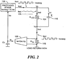
FIG. 2 is a block diagram of a circuit having an open loop response in accordance with an exemplary embodiment; -
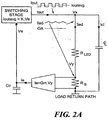
FIG. 2A is a block diagram showing a circuit having an open loop response of greater complexity than the circuit ofFIG. 2 ; -
FIG. 2B is a block diagram of an alternative embodiment of the circuit ofFIG. 2 ; and -
FIG. 3 is a block diagram showing an exemplary implementation of the converter ofFIG. 1 . -
FIG. 1 shows anexemplary circuit 100 having aconverter 102 driving anLED stack 104. Theconverter 102 receives aninput voltage signal 106 to a voltage input terminal VIN and provides agate drive signal 108 on an output terminal SG coupled to aswitching device 110, such as a Field Effect Transistor (FET). Aninductor 114 is coupled between the voltage input terminal VIN and theswitching device 110 with a current limit sense resistor (RSS) 112 coupled between theswitching device 110 and ground. A LED current sense resistor (RSL) 115 is coupled between theLED stack 104 and the voltage input terminal VIN. Aload capacitor 116 is coupled across theLED stack 104. - In the illustrated embodiment, first and second pulse width modulation (PWM) inputs PWM0, PWM1 provide a mechanism to select a PWM dimming level for the
LEDs 104. First and second current select inputs ISET0, ISET1 allow a current level to be selected, as described more fully below. In other embodiments, more and fewer modulation and/or current level inputs are provided to meet the needs of a particular application. - First and second LED current input terminals LN, LP are coupled across the LED current sense resistor (RSL) 115 to provide LED current information to the converter. First and second switch current input terminals SP, SN are coupled across the sense resistor (RSS) 112 to provide switch current information. An LED voltage input terminal VA is coupled to an anode of the
LED stack 104 to provide LED voltage information via a resistor network comprising first and second resistors R1, R2. This enables the output voltage to be limited to a predetermined level, such as 50V.Table 1 below shows an exemplary pinout scheme for the converter 102 of FIG. 1. Table 1 Converter I/OPin Pin Name Pin Description 1 FSEL Frequency compensation select 2 ISET1 Set load current bit I 3 ISET0 Set load current bit 0 4 PWM1 Set PWM dimming bit I 5 PWM0 Set PWM dimming bit 0 6 OSC Oscillator frequency set 7 EN Chip enable 8 FF Fault flag 9 SN Switch current sense -ve input 10 SP Switch current sense +ve input 11 SG Switch gate drive 12 N.C. Connect to 0V 13 GND Ground 14 VREG Internal regulator capacitor 15 N.C. Connect to 5V 16 VIN Main supply 17 LP Load current sense +ve input 18 LN Load current sense -ve input 19 N.C. Not connected 20 VA Voltage limit feedback input - The
converter 102, which can be referred to as a buck-boost DC-DC converter in an exemplary embodiment, provides a programmable constant current output at up to 50V, for example, for drivinghigh power LEDs 104 in series. Driving theLEDs 104 in series ensures identical currents and uniform brightness. For automotive applications, for example, optimum performance is achieved when driving between two and ten LEDs at currents up to 1 A. In one embodiment, a constant frequency, current mode control scheme is used to regulate the current through theLEDs 104. - In an exemplary embodiment, the
LEDs 104 are so-called high current LEDs that can draw for example, a maximum of 1A. Such LEDs can be used for various applications, such as vehicle headlamps. With the high current levels, conventional converters may provide inadequate switching characteristics. Unlike known implementations, the inventive embodiments do not require complex compensation networks that are load dependent. While topologies with comparable response times maybe possible for PWM dimming, such topologies require the user to compensate for the output load pole and zero introduced by an output capacitor. - While the invention is primary described in conjunction with LED applications, it is understood that the invention is applicable to any type of load. In addition, while exemplary embodiments show a load capacitor across the LED stack, it is understood that alternative embodiments include additional impedance components and can have a variety of circuit configurations. Further, while illustrative embodiments show pulse width modulation to control current, it is understood that other modulation techniques, such as frequency modulation, can be used without departing from embodiments of the invention. While so-called high power LEDS are referred to having current ratings in the order of 1A, it is understood that the invention is applicable to loads having any current rating. It is understood that high current LEDs refer to present day standards with the expectation that current ratings will increase in the future. It is contemplated that the inventive embodiments will be applicable to these devices without departing from the invention.
- As shown in
FIG. 2 in conjunction withFIG. 1 , in the illustrated switch-mode current regulating configuration theload capacitor 116 does not interfere with the stability of the compensation loop. The illustratedcircuit 100 has one terminal of the current sense device (RSL) 115 on the node connecting thecapacitor 116 andLED stack 104 together and the other current sense device terminal to the current return path. - This arrangement removes the effect of the
output capacitor 116 on the loop stability. The current sense device (RSL) 115 provides an unfiltered feedback signal that is proportional to the current being output by the switchingstage 130, the average of which is equal to the load current. With this arrangement, the output load and ripple filter capacitor 116 (and equivalent series resistance (ESR) of the capacitor) have no effect on the system stability therefore allowing the user greater flexibility in setting the load resistance and filter capacitance. - As shown, the output current from the switching
stage 130 is a square wave and a current through theLED stack 104 has some degree of ripple. The current across the sense resistor RSL is a square wave. Since theload capacitor 116 is coupled across the LED stack, 104, the open loop response of the circuit in the frequency domain (Laplace transform variable s) is
amplifier 135. Theamplifier 135 outputs a current error signal le corresponding to a voltage Vyacross the sense resistor RSL multiplied by a gain value Gm. Capacitor Cc represents the capacitance of the integrator stage of the feedback loop (seeouter loop 250 andAE 256 ofFIG. 3 below) with an error voltage signal Ve being provided to theswitching stage 130. - In contrast, as shown in the configuration of
FIG. 2A , where a load capacitor is coupled across the LED stack and sense resistor the current though sense resistor Rs is not a square wave and the open loop response is
FIG. 2 . -
FIG. 2B shows an alternative embodiment of the circuit ofFIG. 2 , where like reference numbers indicate like elements. The circuit further includes a resistor R coupled across the series-coupledLED stack 104 andsense resistor RSL 115. A capacitor Copt is coupled across the sense resistor RSL to remove the high frequency edges from the voltage waveform across the sense resistor. The resistor R is intended to show that an extra load can be tapped from the switchingstage 130. That is, current through the sense resistor RSL may not be equal to the current output of the switching element. - High-powered LEDs can be run at average currents that are close to the absolute maximum current rating of the LEDs. As is known in the art, the chromaticity of some LEDs is sensitive to the average current. The inventive method and apparatus embodiments allow the user to trade-off LED current ripple against load capacitor size and cost without being concerned about interfering with the loop stability. Minimizing the effect of the output load on the stability provides a more predictable and therefore higher GBW (gain-bandwidth product) to be set by the dominant pole, thus allowing faster system response to power supply disturbances and other unwanted transients.
-
FIG. 3 shows an exemplary implementation of theconverter 102 ofFIG. 1 , where like reference numbers indicate like elements. Theconverter 102 includes aninner loop 200 that includes an amplifier (AS) 202, comparator (AC) 204, and RSbistable latch 208, to control the inductor current as measured through theswitch 110 by the switch sense resistor (RSS) 112. Theconverter 102 further includes anouter loop 250 having an amplifier (AL) 252 and an integrating error amplifier (AE) 256 to control the average LED current by providing a set point reference for theinner loop 200. - The
LED 104 current is measured by the LED sense resistor (RSL) 115 and compared to a reference current, which is selected by signals to the current level select inputs ISET0, ISET1, to produce an integrated error signal at the output oferror amplifier AE 256. This error signal sets the average amount of energy required from theinductor 114 by the LEDs. The average inductor energy transferred to the LEDs is defined by the average inductor current as determined by theinner control loop 200. - In an exemplary embodiment, the LED current is determined by a combination of the LED sense resistor (RSL) 115, the LED current threshold voltage VIDL, and the current selection logic inputs ISET0 and ISET1 as set forth below in Table 2.
Table 2 LED current settings: ISET1 ISET0 ILED 1 1 100% 1 0 90% 0 1 80% 0 0 70% 
- The
inner loop 200 establishes the average inductor current by controlling the peak switch current on a cycle-by-cycle basis. Since the relationship between peak current and average current is non-linear, depending on the duty cycle, the reference level for the peak switch current is modified by a slope generator 280, which reduces the peak switch current measurement by a small amount as the duty cycle increases. The slope generator 280 compensation also removes the instability inherent in a fixed frequency current control scheme. - In general, the
control loops switch 110 current sensed by the current sense resistor RSS is compared to the LED current error signal. As the LED current increases the output of the error amplifier (AE) 256 will decrease, reducing the peak switch current and thus the current delivered to theLEDs 104. As the LED current decreases the output of the error amplifier (AE) 256 increases, increasing the peak switch current and thus increasing the current delivered to the LEDs. - Under some conditions, especially when the LED current is set to a relatively low value, the energy required in the
inductor 114 may result in the inductor current dropping to zero for part of each cycle. This is known as discontinuous mode operation and will result in some low frequency ripple. The average LED current will however remain regulated down to zero. In discontinuous mode, when the inductor current drops to zero, the voltage at the drain of the external MOSFET will ring due to the resonant LC circuit formed by the inductor and the switch and diode capacitance. This ringing is low frequency and is not harmful. - In an exemplary embodiment, the frequency of the main oscillator is controlled by a single external resistor ROSC(kΩ) between the OSC pin and the GND pin. The oscillator frequency is approximately: fOSC = 2200- (20 x ROSC) kHz. If the OSC pin is left open circuit the oscillator frequency will be set to approximately 1 MHz when FSEL is high or to approximately 250kHz when FSEL is low in one particular embodiment.
- The switch current is measured by the switch sense resistor RSS and the switch sense amplifier (AS) 202. The input limit VIDS of the sense amplifier (AS) 202 and the maximum switch current ISMAX define the maximum value of the sense resistor as: RSS = VIDS ISMAX. This defines the maximum measurable value of the switch (and inductor) current. The peak switch current will always be less than this, set by the control circuit, depending on the required load conditions.
- Although the LED brightness is determined by the current, it may be better to control the brightness by switching the current with a pulse width modulated signal. This allows the LED brightness to be set with little effect on the LED color. In one embodiment, four discrete brightness levels are provided by an internal PWM generator and selected by the logic levels on the PWM0 and PWM1 inputs. Three of the brightness levels provide brightness binning while the third level is lower providing a level for dimming. An exemplary PWM brightness scheme is illustrated in Table 3 below.
Table 3 PWM Brightness Scheme PWM1 PWM0 D 1 1 100% 1 0 87.5% 0 1 75% 0 0 25% 

- External components should be selected to achieve successful application of the LED driver. Although the
inductor 114, switchingMOSFET 110 andoutput capacitor 116 are the primary elements in the illustrative embodiment, the specification of the rectifying diode and sense resistors RSS, RSL should also be considered. In one embodiment, the starting point for component selection is to define the maximum LED current, the voltage across theLEDs 104, and the input operating voltage range. This then allows theaverage inductor 114 current under worst case conditions to be calculated. Theinductor 114 value is then selected based on the acceptable inductor ripple current. The amount of ripple current will then determine the maximum inductor current under worst-case conditions. From this current, the switch current sense resistor RSS can be calculated. - When selecting the switch current sense resistor RSS, neither the absolute value of the switch current nor the accuracy of the measurement is important since the regulator will continuously adjust the switch current, within a closed loop, to provide sufficient energy for the output. For maximum accuracy the switch sense resistor RSS value should be chosen to maximize the differential signal seen by the sense amplifier (AS) 202. The input limit of the sense simplifier, VIDS, and the maximum switch current, ISMAX therefore define the maximum value of the sense resistor as RSS= VIDS/ISMAX, where ISMAX is the maximum switch current and should be set above the maximum inductor current ILPK. This represents the maximum measurable value of the switch (and inductor) current, however, the peak switch current will always be less than this, set by the control circuit, depending on the required load conditions.
- Since the switch current control is within a closed loop, it is possible to reduce the value of the sense resistor RSS to reduce its power dissipation. However this will reduce the accuracy of the regulated LED current.
- In an exemplary embodiment, a logic-level n-channel MOSFET is used as the
switch 110 for the DC-DC converter. The converter topology used is a buck-boost referenced to the positive supply. This means that the voltage at the drain of theMOSFET 110 will reach a voltage equal to the sum of the LED voltage and the supply voltage. Under load dump conditions up to 90V may be present on this node. Theexternal MOSFET 110 should therefore be rated to greater than 100V. The peak switch current is defined by the maximum inductor current ILPK, however in most cases theMOSFET 110 will be chosen by selecting a low on-resistance, which usually results in a current rating of several times the required peak current. In addition to minimizing cost, the choice ofMOSFET 110 should consider both the on-resistance and the total gate charge. The total gate charge will determine the average current required from the internal regulator and thus the power dissipation. - There are a variety of considerations when selecting the
output capacitor 116. The capacitor value is limited by the maximum ripple voltage. In the illustrative switching topology used, theoutput capacitor 116 provides the LED current when theswitch 110 is active. Thecapacitor 116 is then recharged each time theinductor 114 passes energy to the output. The ripple current on theoutput capacitor 116 will be equal to the peak inductor current. The value of theoutput capacitor 110 for the illustrated embodiment will typically be about 10µF and it should be rated above the maximum voltage defined by theseries output LEDs 104. - In general, when operating near, e.g., 80%, of the maximum current rating of the
LEDs 104, the ripple current should be minimized to avoid exceeding the rated current level of the LEDs in the stack. Without theload capacitor 116, theLEDs 104 may see a pure square wave well above the rated value as the circuit is first energized. While theload capacitor 116 filters the current to minimize peaks, the current sensing element RSL sees an unfiltered square wave so that the filtering is separate from the current regulation loop. Thus, thecapacitor 116 does not factor into the regulation scheme described above. - As noted above, the converter limits current even during start up and does not need to wait for the
capacitor 116 to charge. In known configurations, theLEDs 104 may see the maximum current that can be generated by theinductor 114 until current flows though theLED stack 104. The illustrated embodiment avoids current spikes during circuit start up. - The inventive converter can be used in a variety of applications. For example, the converter can energize a stack (e.g., two to ten) of high current (e.g., in the order of 1 A) LEDs. It is understood that any practical number of LEDs having various current ratings can be used. The present embodiments use PWM or other modulation technique to set the brightness of the LEDs by controlling the duty cycle. That is, PWM provides a current level to generate the correct color for the diodes instead of simply 'turning down' the current. For example, at a PWM frequency of 200 Hz (5ms period) with a desired duty cycle of 90% results in 4.5 ms of on time and 0.5 ms of off time, preferably with a square waveform.
- The inventive converter embodiments overcome certain limitations of capacitors. Electrolytic capacitors have a limited ability to handle ripple currents due to a significant equivalent series resistance (ESR) component. Switching current into the electrolytic capacitor can result in unacceptable heating. For high current applications, such as 1A LEDs, this can limit the use of electrolytic capacitors in conventional implementations. While ceramic capacitors can better handle ripple currents due to less heating than electrolytic capacitors, ceramic capacitors are available at limited capacitance values, i.e., in the order of 10µF. The inventive converter eliminates this capacitor ripple current tradeoff required in conventional implementations.
- Having described exemplary embodiments of the invention, it will now become apparent to one of ordinary skill in the art that other embodiments incorporating their concepts, in accordance with the claims, may also be used.
Claims (16)
- A circuit, comprising;
a capacitive element (116) for coupling across a load element (104) to be energized by a DC signal;
a first sense element (115) to monitor an instantaneous sum of currents through the load element and the capacitive element, wherein a first terminal of the first sense element (115) is coupled to a node for connecting the capacitive element (116) and the load element (104) and a second terminal of the first sense element (115) is coupled to a current return path;
a switching element (110) to control current through the first sense element (115);
a second sense element (112) coupled to the switching element (110) to sense current through the switching element (110);
an energy storage element (114) coupled to the switching element (110), a unidirectional current flow element allowing current flow to the load element (104); and
a converter circuit (102) to control the switching element (110);
characterized by that a differential transconductance amplifier (135) having inputs coupled across the first sense element (115), wherein an output (Ie) of the transconductance amplifier (135) contains DC information and is proportional to a current being output by the switching element (110);
a second capacitive element (Cc) coupled to the output of the differential transconductance amplifier (135);
wherein the converter circuit (102) is arranged to regulate to the current level monitored
across the first sense element (115), and wherein a converter regulation loop includes a dominant pole to average the current sensed through the first sense element (115),
wherein the differential transconductance amplifier (135) and the second capacitive element (Cc) provide the active and reactive element for the dominant pole to average the current sensed through the first sense element (115). - The circuit according to claim 1, wherein the circuit comprises a load element and the load element (104) includes an LED stack.
- The circuit according to claim 1, wherein the capacitive element (116) contains a further impedance element (R) coupled in series with the capacitive element (116).
- The circuit according to claim 1, wherein the energy storage element (114) includes an inductor.
- The circuit according to claim 4 wherein the inductor has a first end coupled to the switching element (110) and a second end coupled to an input voltage signal.
- The circuit according to claim 1, wherein the converter circuit (102) comprises switch current terminals coupled across the second sense element (112).
- The circuit according to claim 6 wherein the converter circuit (102) further includes an inner loop (200) coupled to the switch current terminals to control an average energy storage element current by a peak switch current on a cycle-by-cycle basis.
- The circuit according to claim 1, further including a third capacitive element (Copt) coupled in parallel with the first sense element (115) to filter average the current detected by the first sense element (115).
- The circuit of claim 1, wherein:the circuit comprises a load element (104), the load element (104) including an LED stack;the capacitive element (116) is a capacitor;the first sense element (115) is a first current sensing resistor that is coupled in series with the LED stack and the capacitor;the unidirectional current flow element is a blocking diode having an anode and a cathode, the cathode being coupled to the LED stack and the capacitor;the energy storage element (114) includes an inductor having a first end and a second end, the first end being coupled to the anode of the blocking diode and the second end being coupled to an input voltage signal;the switching element (110) is coupled to the blocking diode anode; andthe second sense element (112) is a second current sensing resistor.
- The circuit according to claim 9 wherein the converter circuit (102) includes:first and second terminals coupled across the first current sensing resistor;third and fourth terminals coupled across the second current sensing resistor; anda fifth terminal coupled to the switching element (110) to control current to the LED stack.
- The circuit according to claim 10 further including a sixth terminal to receive a modulation signal.
- The circuit according to claim 11 further including an eighth terminal to receive a current level selection signal.
- The circuit according to claim 10 further including an outer loop (250) coupled to the first and second terminals and an inner loop (200) coupled to the third and fourth terminals.
- A method, comprising:providing a load (104);coupling a capacitive element (116) across the load (104);coupling a first sense element (115) to the load (104) to monitor an instantaneous sum of currents through the load (104) and the capacitive element (116),coupling a first terminal of the first sense element (115) to a node connecting the capacitive element (116) and the load element (104);coupling a second terminal of the first sense element (115) to a current return path;providing a switching element (110) to control a current through the first sense element (115);coupling a second sense element (112) to the switching element (110) to sense a current through the switching element (110);coupling a unidirectional current flow element to the switching element (110) to allow current flow to the load (104);coupling a converter circuit (102) to the switching element (110) to control the switching element (110);coupling an energy storage element (114) to switching element (110); characterized by coupling inputs of a differential transconductance amplifier (135) across the first sense element (115), wherein an output (Ie) of the transconductance amplifier (135) contains DC information and is proportional to a current being output by the switching element (110); andcoupling a second capacitive element (Cc) to the output of the differential transconductance amplifier (135), wherein the differential transconductance amplifier (135) and second capacitive element (Cc) provide an active and reactive element of a dominant pole to average the current sensed through the first sense element (115).
- The method according to claim 14 wherein the converter circuit (102) further includes an inner loop (200) coupled to the switch current terminals to control an average inductor current by a peak switch current on a cycle-by-cycle basis.
- The method according to claim 14 further including coupling a third capacitive element (Copt) in parallel with the first sense element (115) to filter average the current detected by the first sense element (115).
Applications Claiming Priority (2)
| Application Number | Priority Date | Filing Date | Title |
|---|---|---|---|
| US11/396,566 US7649325B2 (en) | 2006-04-03 | 2006-04-03 | Methods and apparatus for switching regulator control |
| PCT/US2007/006875 WO2007126630A2 (en) | 2006-04-03 | 2007-03-20 | Methods and apparatus for switching regulator control |
Publications (2)
| Publication Number | Publication Date |
|---|---|
| EP2011219A2 EP2011219A2 (en) | 2009-01-07 |
| EP2011219B1 true EP2011219B1 (en) | 2017-07-12 |
Family
ID=38557857
Family Applications (1)
| Application Number | Title | Priority Date | Filing Date |
|---|---|---|---|
| EP07753499.8A Not-in-force EP2011219B1 (en) | 2006-04-03 | 2007-03-20 | Methods and apparatus for switching regulator control |
Country Status (4)
| Country | Link |
|---|---|
| US (1) | US7649325B2 (en) |
| EP (1) | EP2011219B1 (en) |
| JP (1) | JP5054759B2 (en) |
| WO (1) | WO2007126630A2 (en) |
Families Citing this family (67)
| Publication number | Priority date | Publication date | Assignee | Title |
|---|---|---|---|---|
| US7659672B2 (en) * | 2006-09-29 | 2010-02-09 | O2Micro International Ltd. | LED driver |
| TWI374419B (en) * | 2007-05-15 | 2012-10-11 | Analog Integrations Corp | Control circuit of area control driving circuit for led light source and controlling method thereof |
| WO2008144961A1 (en) * | 2007-05-31 | 2008-12-04 | Texas Instruments Incorporated | Regulation for led strings |
| DE102007031038A1 (en) * | 2007-07-04 | 2009-01-08 | Tridonicatco Schweiz Ag | Circuit for operating light-emitting diodes (LEDs) |
| US7622871B2 (en) * | 2007-10-01 | 2009-11-24 | Micrel, Incorporated | Light emitting diode driver circuit with shunt switch |
| US7439945B1 (en) * | 2007-10-01 | 2008-10-21 | Micrel, Incorporated | Light emitting diode driver circuit with high-speed pulse width modulated current control |
| US8169161B2 (en) | 2007-11-16 | 2012-05-01 | Allegro Microsystems, Inc. | Electronic circuits for driving series connected light emitting diode strings |
| US7825607B1 (en) * | 2007-11-23 | 2010-11-02 | Zhen Qiu Huang | D-c to d-c converter circuit |
| DE102007057239B4 (en) * | 2007-11-28 | 2013-11-21 | Austriamicrosystems Ag | Circuit arrangement in particular for DC / DC converters and method for controlling such |
| TWM340549U (en) * | 2008-04-01 | 2008-09-11 | Richtek Technology Corp | Apparatus for decreasing internal power loss in integrated circuit package |
| US8487547B2 (en) * | 2008-04-24 | 2013-07-16 | Cypress Semiconductor Corporation | Lighting assembly, circuits and methods |
| US9179509B2 (en) * | 2008-04-24 | 2015-11-03 | Google Inc. | Light emitting diode assembly |
| TW200952541A (en) * | 2008-06-02 | 2009-12-16 | Advanced Analog Technology Inc | LED driver circuit |
| US8093826B1 (en) * | 2008-08-26 | 2012-01-10 | National Semiconductor Corporation | Current mode switcher having novel switch mode control topology and related method |
| TWI396924B (en) * | 2008-12-05 | 2013-05-21 | Skina Optical Co Ltd | Driving control method for having a lens module perform an auto macro function and a driving control system uising in the same |
| US8427075B2 (en) * | 2008-12-12 | 2013-04-23 | Microchip Technology Incorporated | Constant current output sink or source |
| US8378588B2 (en) | 2008-12-12 | 2013-02-19 | O2Micro Inc | Circuits and methods for driving light sources |
| US8076867B2 (en) | 2008-12-12 | 2011-12-13 | O2Micro, Inc. | Driving circuit with continuous dimming function for driving light sources |
| US9253843B2 (en) | 2008-12-12 | 2016-02-02 | 02Micro Inc | Driving circuit with dimming controller for driving light sources |
| US8508150B2 (en) * | 2008-12-12 | 2013-08-13 | O2Micro, Inc. | Controllers, systems and methods for controlling dimming of light sources |
| US9232591B2 (en) | 2008-12-12 | 2016-01-05 | O2Micro Inc. | Circuits and methods for driving light sources |
| US9030122B2 (en) | 2008-12-12 | 2015-05-12 | O2Micro, Inc. | Circuits and methods for driving LED light sources |
| US9386653B2 (en) | 2008-12-12 | 2016-07-05 | O2Micro Inc | Circuits and methods for driving light sources |
| CN102014540B (en) * | 2010-03-04 | 2011-12-28 | 凹凸电子(武汉)有限公司 | Drive circuit and controller for controlling electric power of light source |
| US8044608B2 (en) | 2008-12-12 | 2011-10-25 | O2Micro, Inc | Driving circuit with dimming controller for driving light sources |
| TW201028045A (en) * | 2009-01-09 | 2010-07-16 | Chi Mei Lighting Tech Corp | Light emitting apparatus |
| JP5457684B2 (en) * | 2009-01-20 | 2014-04-02 | 株式会社小糸製作所 | Lighting control device for vehicle lamp |
| US8058812B2 (en) * | 2009-04-09 | 2011-11-15 | Linear Technology Corporation | Buck-mode boost converter with regulated output current |
| DE102009017139A1 (en) * | 2009-04-14 | 2010-10-21 | Tridonicatco Gmbh & Co. Kg | LED e.g. organic LED, regulating method for illumination system, involves utilizing measured actual value as feedback variable for regulation of LED, where actual value is compared with reference value |
| US9060406B2 (en) | 2009-04-14 | 2015-06-16 | Tridonic Gmbh And Co Kg | Power regulation of LED by means of an average value of the LED current and bidirectional counter |
| AT508195B1 (en) * | 2009-04-30 | 2012-03-15 | Tridonic Gmbh & Co Kg | OPERATING CIRCUIT FOR LIGHT DIODES |
| TW201130379A (en) * | 2009-08-26 | 2011-09-01 | Koninkl Philips Electronics Nv | Method and apparatus for controlling dimming levels of LEDs |
| CN103391006A (en) | 2012-05-11 | 2013-11-13 | 凹凸电子(武汉)有限公司 | Light source driving circuit and controller and method for controlling power converter |
| US8698419B2 (en) | 2010-03-04 | 2014-04-15 | O2Micro, Inc. | Circuits and methods for driving light sources |
| JP2012070556A (en) * | 2010-09-24 | 2012-04-05 | Sanken Electric Co Ltd | Dc power supply device |
| US8476842B2 (en) * | 2010-12-08 | 2013-07-02 | Excelliance Mos Corporation | Driving device for LED module |
| US8692482B2 (en) | 2010-12-13 | 2014-04-08 | Allegro Microsystems, Llc | Circuitry to control a switching regulator |
| US8598810B2 (en) * | 2011-05-05 | 2013-12-03 | Excelliance Mos Corporation | Constant current driving circuit of light emitting diode and lighting apparatus |
| CN102769960A (en) * | 2011-05-06 | 2012-11-07 | 欧司朗股份有限公司 | Dimmable type LED (Light Emitting Diode) driver and control method of dimmable type LED driver |
| WO2012164787A1 (en) * | 2011-06-03 | 2012-12-06 | パナソニック株式会社 | Buck-boost converter |
| CN102821510B (en) * | 2011-06-08 | 2014-11-05 | 聚积科技股份有限公司 | AC/DC dual-purpose LED drive circuit |
| CN102821509A (en) * | 2011-06-08 | 2012-12-12 | 聚积科技股份有限公司 | AC/DC dual-purpose LED drive circuit |
| KR101798437B1 (en) * | 2011-06-16 | 2017-11-16 | 삼성전자주식회사 | Light emitting diode driver circuit and method for light emitting diode driving |
| US8680783B2 (en) * | 2011-08-10 | 2014-03-25 | Cree, Inc. | Bias voltage generation using a load in series with a switch |
| US9272659B1 (en) * | 2011-11-04 | 2016-03-01 | Marcus C. Boykin | Auxiliary vehicle lamp operation system |
| CN104106312B (en) * | 2011-12-05 | 2017-01-18 | 埃尔多实验室控股有限公司 | Driver system for driving at least one led |
| WO2013098704A1 (en) * | 2011-12-28 | 2013-07-04 | Osram Gmbh | Converter device |
| US9155139B2 (en) | 2012-03-09 | 2015-10-06 | Rockwell Automation Technologies, Inc. | LED driver circuits and methods |
| US9144126B2 (en) | 2012-08-22 | 2015-09-22 | Allegro Microsystems, Llc | LED driver having priority queue to track dominant LED channel |
| US8957607B2 (en) | 2012-08-22 | 2015-02-17 | Allergo Microsystems, LLC | DC-DC converter using hysteretic control and associated methods |
| AT514028B1 (en) * | 2013-03-07 | 2017-02-15 | Dipl Ing Dr Himmelstoss Felix | Opto driver stages with rapid increase in current in the light-emitting components |
| JP6111508B2 (en) * | 2013-08-22 | 2017-04-12 | パナソニックIpマネジメント株式会社 | Lighting device and lighting fixture using the same |
| AT14187U1 (en) * | 2013-11-14 | 2015-05-15 | Tridonic Gmbh & Co Kg | Operating circuit for a luminous means and method for operating a light source |
| EP2873980B1 (en) * | 2013-11-19 | 2019-04-10 | Dialog Semiconductor GmbH | Current limit control with constant accuracy |
| US20150207399A1 (en) * | 2014-01-20 | 2015-07-23 | Immense Advance Technology Corp. | Pwm controller capable of controlling output current ripple via a resistor, and led driver circuit using same |
| US9351352B2 (en) * | 2014-04-03 | 2016-05-24 | Linear Technology Corporation | Boost then floating buck mode converter for LED driver using common switch control signal |
| CN106028577A (en) * | 2016-08-02 | 2016-10-12 | 惠勇 | A kind of LED drive dimming rectification circuit |
| RU2693844C1 (en) * | 2018-09-04 | 2019-07-05 | Акционерное общество "Научно-Производственный Комплекс "Альфа-М" | Method to control light output level of light-emitting diodes and device for its implementation |
| CN111432529B (en) * | 2020-03-17 | 2022-10-21 | 成都芯源系统有限公司 | Control circuit and control method of true zero current dimming circuit |
| US10999906B1 (en) * | 2020-03-18 | 2021-05-04 | Xiamen Eco Lighting Co. Ltd. | Self-adaptive illuminating device |
| US11082038B1 (en) | 2020-09-10 | 2021-08-03 | Allegro Microsystems, Llc | Gate driver isolating circuit |
| US11075622B1 (en) | 2020-09-10 | 2021-07-27 | Allegro Microsystems, Llc | Switch turn on in a gate driver circuit |
| CN112040608B (en) | 2020-09-16 | 2022-10-18 | 英飞特电子(杭州)股份有限公司 | LED control circuit and LED lighting system |
| US11025247B1 (en) | 2020-10-08 | 2021-06-01 | Allegro Microsystems, Llc | Gate driver circuit providing an output voltage that is clamped |
| CN113098271B (en) * | 2021-04-23 | 2022-05-27 | 南京理工大学 | High-gain three-port DC-DC converter based on switch capacitor |
| US11770072B2 (en) | 2021-10-26 | 2023-09-26 | Allegro Microsystems, Llc | Commonly controlled buck-boost converter |
| US12308744B2 (en) | 2022-10-26 | 2025-05-20 | Allegro Microsystems, Llc | Adaptive current limiter |
Citations (3)
| Publication number | Priority date | Publication date | Assignee | Title |
|---|---|---|---|---|
| US5804950A (en) * | 1996-06-20 | 1998-09-08 | Micro Linear Corporation | Input current modulation for power factor correction |
| US20040012376A1 (en) * | 2000-09-04 | 2004-01-22 | Karim-Thomas Taghizadeh-Kaschani | Current-mode switching regulator |
| WO2005031956A1 (en) * | 2003-09-25 | 2005-04-07 | Koninklijke Philips Electronics N.V. | A switch mode power converter |
Family Cites Families (19)
| Publication number | Priority date | Publication date | Assignee | Title |
|---|---|---|---|---|
| US5204639A (en) * | 1992-04-27 | 1993-04-20 | Motorola, Inc. | Miller loop compensation network with capacitive drive |
| US5481178A (en) * | 1993-03-23 | 1996-01-02 | Linear Technology Corporation | Control circuit and method for maintaining high efficiency over broad current ranges in a switching regulator circuit |
| US5414341A (en) * | 1993-12-07 | 1995-05-09 | Benchmarq Microelectronics, Inc. | DC-DC converter operable in an asyncronous or syncronous or linear mode |
| US6011431A (en) * | 1994-11-23 | 2000-01-04 | Analog Devices, Inc. | Automatically tracking multiple-pole active filter |
| US5600234A (en) * | 1995-03-01 | 1997-02-04 | Texas Instruments Incorporated | Switch mode power converter and method |
| IT1296072B1 (en) * | 1997-11-06 | 1999-06-09 | Sgs Thomson Microelectronics | CURRENT DETECTION CIRCUIT WITH HIGH INPUT IMPEDANCE |
| US6307356B1 (en) * | 1998-06-18 | 2001-10-23 | Linear Technology Corporation | Voltage mode feedback burst mode circuit |
| US6144194A (en) * | 1998-07-13 | 2000-11-07 | Linear Technology Corp. | Polyphase synchronous switching voltage regulators |
| US6208279B1 (en) * | 1998-08-17 | 2001-03-27 | Linear Technology Dorporation | Single-cycle oversampling analog-to-digital converter |
| US6285246B1 (en) * | 1998-09-15 | 2001-09-04 | California Micro Devices, Inc. | Low drop-out regulator capable of functioning in linear and saturated regions of output driver |
| US6100678A (en) * | 1999-08-26 | 2000-08-08 | Linear Technology Corporation | Single package pin providing soft-start and short-circuit timer functions in a voltage regulator controller |
| US6674274B2 (en) * | 2001-02-08 | 2004-01-06 | Linear Technology Corporation | Multiple phase switching regulators with stage shedding |
| US6518733B1 (en) * | 2001-08-03 | 2003-02-11 | Linear Technology Corporation | Circuits and techniques for capacitor charging circuits |
| US6424129B1 (en) * | 2001-08-21 | 2002-07-23 | Semtech Corporation | Method and apparatus for accurately sensing output current in a DC-to-DC voltage converter |
| US7042207B1 (en) * | 2003-11-07 | 2006-05-09 | National Semiconductor Corporation | Inductive measurement system and method |
| JP4052998B2 (en) * | 2003-11-25 | 2008-02-27 | シャープ株式会社 | Power supply circuit and electronic device using the same |
| US7459864B2 (en) * | 2004-03-15 | 2008-12-02 | Philips Solid-State Lighting Solutions, Inc. | Power control methods and apparatus |
| US7233258B1 (en) * | 2004-04-13 | 2007-06-19 | Gelcore Llc | LED matrix current control |
| US7990120B2 (en) * | 2006-08-04 | 2011-08-02 | Linear Technology Corporation | Circuits and methods for adjustable peak inductor current and hysteresis for burst mode in switching regulators |
-
2006
- 2006-04-03 US US11/396,566 patent/US7649325B2/en active Active
-
2007
- 2007-03-20 JP JP2009504197A patent/JP5054759B2/en not_active Expired - Fee Related
- 2007-03-20 WO PCT/US2007/006875 patent/WO2007126630A2/en not_active Ceased
- 2007-03-20 EP EP07753499.8A patent/EP2011219B1/en not_active Not-in-force
Patent Citations (3)
| Publication number | Priority date | Publication date | Assignee | Title |
|---|---|---|---|---|
| US5804950A (en) * | 1996-06-20 | 1998-09-08 | Micro Linear Corporation | Input current modulation for power factor correction |
| US20040012376A1 (en) * | 2000-09-04 | 2004-01-22 | Karim-Thomas Taghizadeh-Kaschani | Current-mode switching regulator |
| WO2005031956A1 (en) * | 2003-09-25 | 2005-04-07 | Koninklijke Philips Electronics N.V. | A switch mode power converter |
Also Published As
| Publication number | Publication date |
|---|---|
| WO2007126630A3 (en) | 2008-04-03 |
| EP2011219A2 (en) | 2009-01-07 |
| JP5054759B2 (en) | 2012-10-24 |
| US20070229001A1 (en) | 2007-10-04 |
| WO2007126630A2 (en) | 2007-11-08 |
| JP2009533015A (en) | 2009-09-10 |
| US7649325B2 (en) | 2010-01-19 |
Similar Documents
| Publication | Publication Date | Title |
|---|---|---|
| US7649325B2 (en) | Methods and apparatus for switching regulator control | |
| US10178719B2 (en) | Biasing and driving circuit, based on a feedback voltage regulator, for an electric load | |
| JP5514337B2 (en) | Drive device | |
| US9013165B2 (en) | Switching regulator including a configurable multi-mode PWM controller implementing multiple control schemes | |
| US9253832B2 (en) | Power supply circuit with a control terminal for different functional modes of operation | |
| US8698419B2 (en) | Circuits and methods for driving light sources | |
| US8891255B2 (en) | Switching power supply apparatus including simultanous control of multiple outputs | |
| US20150015226A1 (en) | Current Driver Circuit | |
| US20100194368A1 (en) | Current driving method and circuit | |
| US20120268023A1 (en) | Circuits and methods for driving light sources | |
| US20210391789A1 (en) | Driving Device | |
| KR20080023648A (en) | How to generate ripple in buck regulator using fixed on-time to use output capacitor with any ESR | |
| WO2005112240A2 (en) | High efficiency linear regulator | |
| US20160044759A1 (en) | Multichannel constant current led controlling circuit and controlling method | |
| US20120262079A1 (en) | Circuits and methods for driving light sources | |
| JP6154584B2 (en) | Power supply device, and in-vehicle device and vehicle using the same | |
| US20120187995A1 (en) | Error amplification circuit, control method for error amplification circuit, and switching regulator employing error amplification circuit | |
| CN114094999A (en) | Converter circuit, corresponding device and method | |
| GB2497213A (en) | Circuits and methods for driving light sources | |
| GB2503316A (en) | Circuits and methods for driving light sources | |
| Sengupta | PWM and PFM operation of DC/DC converters for portable applications | |
| US7495424B1 (en) | Overload compensation circuit with improved recovery response for a power supply | |
| JP2004147418A (en) | Switching power supply and power supply system | |
| EP2501025B1 (en) | Power supply circuit comprising two DC/DC converters |
Legal Events
| Date | Code | Title | Description |
|---|---|---|---|
| PUAI | Public reference made under article 153(3) epc to a published international application that has entered the european phase |
Free format text: ORIGINAL CODE: 0009012 |
|
| 17P | Request for examination filed |
Effective date: 20081031 |
|
| AK | Designated contracting states |
Kind code of ref document: A2 Designated state(s): AT BE BG CH CY CZ DE DK EE ES FI FR GB GR HU IE IS IT LI LT LU LV MC MT NL PL PT RO SE SI SK TR |
|
| AX | Request for extension of the european patent |
Extension state: AL BA HR MK RS |
|
| 17Q | First examination report despatched |
Effective date: 20120418 |
|
| DAX | Request for extension of the european patent (deleted) | ||
| RAP1 | Party data changed (applicant data changed or rights of an application transferred) |
Owner name: ALLEGRO MICROSYSTEMS, LLC |
|
| STAA | Information on the status of an ep patent application or granted ep patent |
Free format text: STATUS: EXAMINATION IS IN PROGRESS |
|
| GRAP | Despatch of communication of intention to grant a patent |
Free format text: ORIGINAL CODE: EPIDOSNIGR1 |
|
| STAA | Information on the status of an ep patent application or granted ep patent |
Free format text: STATUS: GRANT OF PATENT IS INTENDED |
|
| RIC1 | Information provided on ipc code assigned before grant |
Ipc: H05B 33/08 20060101ALN20170214BHEP Ipc: H02M 3/156 20060101AFI20170214BHEP |
|
| RIC1 | Information provided on ipc code assigned before grant |
Ipc: H05B 33/08 20060101ALN20170227BHEP Ipc: H02M 3/156 20060101AFI20170227BHEP |
|
| INTG | Intention to grant announced |
Effective date: 20170313 |
|
| GRAS | Grant fee paid |
Free format text: ORIGINAL CODE: EPIDOSNIGR3 |
|
| GRAA | (expected) grant |
Free format text: ORIGINAL CODE: 0009210 |
|
| STAA | Information on the status of an ep patent application or granted ep patent |
Free format text: STATUS: THE PATENT HAS BEEN GRANTED |
|
| AK | Designated contracting states |
Kind code of ref document: B1 Designated state(s): AT BE BG CH CY CZ DE DK EE ES FI FR GB GR HU IE IS IT LI LT LU LV MC MT NL PL PT RO SE SI SK TR |
|
| REG | Reference to a national code |
Ref country code: GB Ref legal event code: FG4D |
|
| REG | Reference to a national code |
Ref country code: CH Ref legal event code: EP |
|
| REG | Reference to a national code |
Ref country code: AT Ref legal event code: REF Ref document number: 909194 Country of ref document: AT Kind code of ref document: T Effective date: 20170715 |
|
| REG | Reference to a national code |
Ref country code: IE Ref legal event code: FG4D |
|
| REG | Reference to a national code |
Ref country code: DE Ref legal event code: R096 Ref document number: 602007051612 Country of ref document: DE |
|
| REG | Reference to a national code |
Ref country code: NL Ref legal event code: MP Effective date: 20170712 |
|
| REG | Reference to a national code |
Ref country code: LT Ref legal event code: MG4D |
|
| REG | Reference to a national code |
Ref country code: AT Ref legal event code: MK05 Ref document number: 909194 Country of ref document: AT Kind code of ref document: T Effective date: 20170712 |
|
| PG25 | Lapsed in a contracting state [announced via postgrant information from national office to epo] |
Ref country code: AT Free format text: LAPSE BECAUSE OF FAILURE TO SUBMIT A TRANSLATION OF THE DESCRIPTION OR TO PAY THE FEE WITHIN THE PRESCRIBED TIME-LIMIT Effective date: 20170712 Ref country code: LT Free format text: LAPSE BECAUSE OF FAILURE TO SUBMIT A TRANSLATION OF THE DESCRIPTION OR TO PAY THE FEE WITHIN THE PRESCRIBED TIME-LIMIT Effective date: 20170712 Ref country code: NL Free format text: LAPSE BECAUSE OF FAILURE TO SUBMIT A TRANSLATION OF THE DESCRIPTION OR TO PAY THE FEE WITHIN THE PRESCRIBED TIME-LIMIT Effective date: 20170712 Ref country code: SE Free format text: LAPSE BECAUSE OF FAILURE TO SUBMIT A TRANSLATION OF THE DESCRIPTION OR TO PAY THE FEE WITHIN THE PRESCRIBED TIME-LIMIT Effective date: 20170712 Ref country code: FI Free format text: LAPSE BECAUSE OF FAILURE TO SUBMIT A TRANSLATION OF THE DESCRIPTION OR TO PAY THE FEE WITHIN THE PRESCRIBED TIME-LIMIT Effective date: 20170712 |
|
| PG25 | Lapsed in a contracting state [announced via postgrant information from national office to epo] |
Ref country code: ES Free format text: LAPSE BECAUSE OF FAILURE TO SUBMIT A TRANSLATION OF THE DESCRIPTION OR TO PAY THE FEE WITHIN THE PRESCRIBED TIME-LIMIT Effective date: 20170712 Ref country code: LV Free format text: LAPSE BECAUSE OF FAILURE TO SUBMIT A TRANSLATION OF THE DESCRIPTION OR TO PAY THE FEE WITHIN THE PRESCRIBED TIME-LIMIT Effective date: 20170712 Ref country code: GR Free format text: LAPSE BECAUSE OF FAILURE TO SUBMIT A TRANSLATION OF THE DESCRIPTION OR TO PAY THE FEE WITHIN THE PRESCRIBED TIME-LIMIT Effective date: 20171013 Ref country code: PL Free format text: LAPSE BECAUSE OF FAILURE TO SUBMIT A TRANSLATION OF THE DESCRIPTION OR TO PAY THE FEE WITHIN THE PRESCRIBED TIME-LIMIT Effective date: 20170712 Ref country code: IS Free format text: LAPSE BECAUSE OF FAILURE TO SUBMIT A TRANSLATION OF THE DESCRIPTION OR TO PAY THE FEE WITHIN THE PRESCRIBED TIME-LIMIT Effective date: 20171112 Ref country code: BG Free format text: LAPSE BECAUSE OF FAILURE TO SUBMIT A TRANSLATION OF THE DESCRIPTION OR TO PAY THE FEE WITHIN THE PRESCRIBED TIME-LIMIT Effective date: 20171012 |
|
| REG | Reference to a national code |
Ref country code: DE Ref legal event code: R097 Ref document number: 602007051612 Country of ref document: DE |
|
| PG25 | Lapsed in a contracting state [announced via postgrant information from national office to epo] |
Ref country code: RO Free format text: LAPSE BECAUSE OF FAILURE TO SUBMIT A TRANSLATION OF THE DESCRIPTION OR TO PAY THE FEE WITHIN THE PRESCRIBED TIME-LIMIT Effective date: 20170712 Ref country code: DK Free format text: LAPSE BECAUSE OF FAILURE TO SUBMIT A TRANSLATION OF THE DESCRIPTION OR TO PAY THE FEE WITHIN THE PRESCRIBED TIME-LIMIT Effective date: 20170712 Ref country code: CZ Free format text: LAPSE BECAUSE OF FAILURE TO SUBMIT A TRANSLATION OF THE DESCRIPTION OR TO PAY THE FEE WITHIN THE PRESCRIBED TIME-LIMIT Effective date: 20170712 |
|
| PLBE | No opposition filed within time limit |
Free format text: ORIGINAL CODE: 0009261 |
|
| STAA | Information on the status of an ep patent application or granted ep patent |
Free format text: STATUS: NO OPPOSITION FILED WITHIN TIME LIMIT |
|
| PG25 | Lapsed in a contracting state [announced via postgrant information from national office to epo] |
Ref country code: SK Free format text: LAPSE BECAUSE OF FAILURE TO SUBMIT A TRANSLATION OF THE DESCRIPTION OR TO PAY THE FEE WITHIN THE PRESCRIBED TIME-LIMIT Effective date: 20170712 Ref country code: EE Free format text: LAPSE BECAUSE OF FAILURE TO SUBMIT A TRANSLATION OF THE DESCRIPTION OR TO PAY THE FEE WITHIN THE PRESCRIBED TIME-LIMIT Effective date: 20170712 Ref country code: IT Free format text: LAPSE BECAUSE OF FAILURE TO SUBMIT A TRANSLATION OF THE DESCRIPTION OR TO PAY THE FEE WITHIN THE PRESCRIBED TIME-LIMIT Effective date: 20170712 |
|
| 26N | No opposition filed |
Effective date: 20180413 |
|
| PG25 | Lapsed in a contracting state [announced via postgrant information from national office to epo] |
Ref country code: SI Free format text: LAPSE BECAUSE OF FAILURE TO SUBMIT A TRANSLATION OF THE DESCRIPTION OR TO PAY THE FEE WITHIN THE PRESCRIBED TIME-LIMIT Effective date: 20170712 |
|
| REG | Reference to a national code |
Ref country code: CH Ref legal event code: PL |
|
| GBPC | Gb: european patent ceased through non-payment of renewal fee |
Effective date: 20180320 |
|
| PG25 | Lapsed in a contracting state [announced via postgrant information from national office to epo] |
Ref country code: MC Free format text: LAPSE BECAUSE OF FAILURE TO SUBMIT A TRANSLATION OF THE DESCRIPTION OR TO PAY THE FEE WITHIN THE PRESCRIBED TIME-LIMIT Effective date: 20170712 |
|
| REG | Reference to a national code |
Ref country code: BE Ref legal event code: MM Effective date: 20180331 |
|
| REG | Reference to a national code |
Ref country code: IE Ref legal event code: MM4A |
|
| PG25 | Lapsed in a contracting state [announced via postgrant information from national office to epo] |
Ref country code: LU Free format text: LAPSE BECAUSE OF NON-PAYMENT OF DUE FEES Effective date: 20180320 |
|
| PG25 | Lapsed in a contracting state [announced via postgrant information from national office to epo] |
Ref country code: IE Free format text: LAPSE BECAUSE OF NON-PAYMENT OF DUE FEES Effective date: 20180320 |
|
| PG25 | Lapsed in a contracting state [announced via postgrant information from national office to epo] |
Ref country code: CH Free format text: LAPSE BECAUSE OF NON-PAYMENT OF DUE FEES Effective date: 20180331 Ref country code: LI Free format text: LAPSE BECAUSE OF NON-PAYMENT OF DUE FEES Effective date: 20180331 Ref country code: GB Free format text: LAPSE BECAUSE OF NON-PAYMENT OF DUE FEES Effective date: 20180320 Ref country code: BE Free format text: LAPSE BECAUSE OF NON-PAYMENT OF DUE FEES Effective date: 20180331 |
|
| PG25 | Lapsed in a contracting state [announced via postgrant information from national office to epo] |
Ref country code: FR Free format text: LAPSE BECAUSE OF NON-PAYMENT OF DUE FEES Effective date: 20180331 |
|
| PG25 | Lapsed in a contracting state [announced via postgrant information from national office to epo] |
Ref country code: MT Free format text: LAPSE BECAUSE OF NON-PAYMENT OF DUE FEES Effective date: 20180320 |
|
| PG25 | Lapsed in a contracting state [announced via postgrant information from national office to epo] |
Ref country code: TR Free format text: LAPSE BECAUSE OF FAILURE TO SUBMIT A TRANSLATION OF THE DESCRIPTION OR TO PAY THE FEE WITHIN THE PRESCRIBED TIME-LIMIT Effective date: 20170712 |
|
| PG25 | Lapsed in a contracting state [announced via postgrant information from national office to epo] |
Ref country code: PT Free format text: LAPSE BECAUSE OF FAILURE TO SUBMIT A TRANSLATION OF THE DESCRIPTION OR TO PAY THE FEE WITHIN THE PRESCRIBED TIME-LIMIT Effective date: 20170712 Ref country code: HU Free format text: LAPSE BECAUSE OF FAILURE TO SUBMIT A TRANSLATION OF THE DESCRIPTION OR TO PAY THE FEE WITHIN THE PRESCRIBED TIME-LIMIT; INVALID AB INITIO Effective date: 20070320 |
|
| PG25 | Lapsed in a contracting state [announced via postgrant information from national office to epo] |
Ref country code: CY Free format text: LAPSE BECAUSE OF FAILURE TO SUBMIT A TRANSLATION OF THE DESCRIPTION OR TO PAY THE FEE WITHIN THE PRESCRIBED TIME-LIMIT Effective date: 20170712 |
|
| PGFP | Annual fee paid to national office [announced via postgrant information from national office to epo] |
Ref country code: DE Payment date: 20231229 Year of fee payment: 18 |
|
| REG | Reference to a national code |
Ref country code: DE Ref legal event code: R119 Ref document number: 602007051612 Country of ref document: DE |
|
| PG25 | Lapsed in a contracting state [announced via postgrant information from national office to epo] |
Ref country code: DE Free format text: LAPSE BECAUSE OF NON-PAYMENT OF DUE FEES Effective date: 20251001 |