EP2008966A2 - MEMS device formed inside hermetic chamber having getter film - Google Patents
MEMS device formed inside hermetic chamber having getter film Download PDFInfo
- Publication number
- EP2008966A2 EP2008966A2 EP08252173A EP08252173A EP2008966A2 EP 2008966 A2 EP2008966 A2 EP 2008966A2 EP 08252173 A EP08252173 A EP 08252173A EP 08252173 A EP08252173 A EP 08252173A EP 2008966 A2 EP2008966 A2 EP 2008966A2
- Authority
- EP
- European Patent Office
- Prior art keywords
- mems device
- getter film
- cavity
- glass substrate
- getter
- Prior art date
- Legal status (The legal status is an assumption and is not a legal conclusion. Google has not performed a legal analysis and makes no representation as to the accuracy of the status listed.)
- Withdrawn
Links
Images




Classifications
-
- B—PERFORMING OPERATIONS; TRANSPORTING
- B81—MICROSTRUCTURAL TECHNOLOGY
- B81B—MICROSTRUCTURAL DEVICES OR SYSTEMS, e.g. MICROMECHANICAL DEVICES
- B81B7/00—Microstructural systems ; Auxiliary parts of microstructural devices or systems
- B81B7/0032—Packages or encapsulation
- B81B7/0035—Packages or encapsulation for maintaining a controlled atmosphere inside of the chamber containing the MEMS
- B81B7/0038—Packages or encapsulation for maintaining a controlled atmosphere inside of the chamber containing the MEMS using materials for controlling the level of pressure, contaminants or moisture inside of the package, e.g. getters
Definitions
- the present invention relates to a Micro Electro Mechanical Systems (MEMS) device formed inside a hermetic chamber having a getter film.
- MEMS Micro Electro Mechanical Systems
- MEMS devices are rapidly progressing in a growing number of technical fields.
- MEMS devices are utilized not only in micro turbines and sensors, but also in communications and medical fields.
- Getter technology represents a fundamental element of MEMS technology. Getters are important for stabilizing a performance of MEMS devices formed inside hermetic chambers. Improved getter technology is indispensable to an advancement of many fields, especially fields requiring miniaturization in applications such as sensors.
- getters are formed by vapor deposition on a bottom of a cavity made in a glass substrate.
- a hermetic chamber is formed, for example, by bonding silicon and glass substrates by anodic bonding.
- the getter absorbs an amount of oxygen or other residual gases remaining after the anodic bonding, as described in Japanese Published Unexamined Patent Application No. 10-122869 .
- Japanese Published Unexamined Patent Application No. 10-213441 discusses a method of reactivating a getter formed on a bottom of a cavity made in a glass substrate, wherein the reactivation is performed after sealing the chamber by applying difference in electrical potentials to the getter to produce an electric current therein.
- a location of the getter film inside the hermetic chamber may affect various aspects of performance of the MEMS device. For example, in the case where a portion of a getter is too close to an electrode formed on a MEMS device, even though no physical contact is made therebetween, electric noise may transmit from the electrode via the getter film coupled capacitively to an electrode of a sensor or a driver, thereby impairing the operation of the MEMS device.
- a miniature MEMS device is utilized in, for example, a resonator gyroscope chip having a substantially square cross-section occupying 100 mm 2 or less when viewed from the front, as illustrated in Fig. 1 .
- the miniaturization of a device requires a smaller volume of hermetic chamber. Gases such as residual gases and gases released into the hermetic chamber during production remain inside the hermetic chamber. The smaller hermetic chamber volume results in stronger influences of these gases on the pressure inside the hermetic chamber. As a result, a detection sensitivity of a MEMS sensor, for example, may be noticeably impaired.
- the technical significance of the getter region for miniature MEMS devices is particularly high. Unfortunately, it is very difficult to form conventional getters that solve the problems recited above while maintaining the required gas absorption capabilities.
- the present invention is directed to solve the above recited technical obstacles, thereby greatly contributing to the optimization of the spatial relationship between a MEMS device formed inside a hermetic chamber and a getter useful for maintaining the performance thereof.
- the inventors focused firstly made a cavity in a substrate to form a hermetic cavity and focused on the depth of the cavity in the case where a getter region is formed on the bottom of the cavity. As a result of various experiments, it became apparent that a technical dilemma exists relating to a position of the getter region and the cavity depth.
- Fig. 12 is a partial cross-sectional view of a conventional ring or hoop-like shape resonator gyroscope 700 along the C-C line of Fig. 2 .
- One MEMS device includes a movable portion and a fixed portion formed inside a hermetic chamber.
- the hermetic chamber is formed by a glass substrate having a cavity made therein and a base material of the MEMS device.
- One or a plurality of getter films are formed inside the hermetic chamber and interconnect therein. A portion of the getter film is connected via the base material of the MEMS device to only one of any one or a plurality of predetermined electrical potentials of the fixed portion and a ground potential of the fixed portion.
- the getter film is not limited to a continuous single entity or one interconnected getter film.
- getter films may be divided into a plurality of regions. Even in a case where the getter film is divided into a plurality of regions, each getter film connects via the base material of the MEMS device to only one predetermined electrical potential or only a ground potential, respectively. In order words, each of the continuous getter films may not connect simultaneously to two predetermined electrical potentials having a difference therebetween.
- the scope of the present invention includes the case where the getter films are divided into a plurality of regions, each region connects to a predetermined electrical potential (including a ground potential), respectively, and the predetermined electrical potentials differ from one another.
- the getter film is formed inside the hermetic chamber and connected to only one predetermined electrical potential or a ground potential, thereby preventing the potential of the getter film from so-called floating even during the operation of the MEMS device. Therefore, even in the case where the getter film is formed near an electrode of the MEMS device, the electrical potential applied to the getter is stabilized, thereby preventing the transmission of electric noise from the electrode through the getter to an electrode of a sensor or a driver.
- the cavity made in the glass substrate for forming the hermetic chamber can be made much shallower than that of conventional art. Therefore, less processing time, simpler manufacturing steps, and greatly reducing manufacturing costs can be achieved.
- Another MEMS device includes a movable portion and a fixed portion formed inside a hermetic chamber.
- the hermetic chamber is formed by a glass substrate having a cavity made therein and a base material of the MEMS device.
- a getter film is formed on a bottom and a side surface, or a side surface of the cavity. The getter film extends from the at least one of the bottom surfaces and the side surfaces via a surface of a support of the glass substrate for supporting the MEMS device, contacting to a surface of at least a portion of the fixed portion connecting to only any one or a plurality of predetermined electrical potentials.
- Yet another MEMS device includes a movable portion and a fixed portion formed inside a hermetic chamber.
- the hermetic chamber is formed by a glass substrate having a cavity made therein and a base material of the MEMS device.
- a getter film is formed on a bottom and a side surface, or a side surface of the cavity. The getter film on the bottom and/or the side surface of the cavity extends to a surface of at least a portion of the fixed portion and contacts thereto, the fixed portion being connected to only one ground potential.
- the getter film formed inside the hermetic chamber is connected to only one or a plurality of predetermined electrical potentials, thereby preventing the potential of the getter film from floating even during the operation of the MEMS device. Therefore, even in the case where the getter film is formed near each of electrodes of the MEMS device, the electrical potential applied to the getter film is stabilized, thereby preventing the transmission of electric noise from the electrode via the getter to an electrode of a sensor or a driver.
- the cavity made in the glass substrate for forming the hermetic chamber can be made much shallower than that of conventional art. Therefore, less processing time, simpler manufacturing steps, and greatly reducing manufacturing costs can be achieved.
- Connecting the getter film to only a ground potential provides a more stable potential than connecting the getter film to only a predetermined electrical potential other than a ground potential, thereby further reducing electric noise transmitted to the electrodes of the sensors or the drivers, thus providing more favorable characteristics.
- the fixed portion of the present invention may be a portion or an entirety of a non-moving member having a prescribed role in the MEMS device including an electrical effect, a physical effect, or an advantage during a manufacturing process.
- the non-moving member having the prescribed role may in its entirety be the fixed portion, or may include only a portion that is the fixed portion.
- a getter film material including at least one non-evaporable metal selected from the group consisting of titanium, zirconium, vanadium, aluminum, tantalum, tungsten, and molybdenum.
- a getter film is formed inside a hermetic chamber and connected to only one predetermined electrical potential or ground potential, thereby preventing the potential of the getter film from floating even during the operation of the MEMS device. Therefore, even in the case where the getter film is formed near an electrode of the MEMS device, the electrical potential applied to the getter is stabilized, thereby preventing a transmission of electric noise from the electrode through the getter to an electrode of a sensor or a driver.
- the cavity made in the glass substrate for forming the hermetic chamber can be made much shallower than that of conventional art. Therefore, less processing time, simpler manufacturing steps, and greatly reducing manufacturing costs can be achieved.
- a MEMS device i.e., a ring or hoop-like shape resonator gyroscope 100
- Fig. 1 is a partially enlarged view of the A-A quadrant of Fig. 1
- Fig. 3 is a cross-sectional view along the B-B line of Fig. 1
- Fig. 4 is an exploded perspective view of the ring or hoop-like shape resonator gyroscope 100 according to this exemplary embodiment, including a package.
- the MEMS device is the ring or hoop-like shape resonator gyroscope 100.
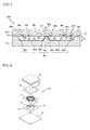
- the ring or hoop-like shape resonator gyroscope 100 includes: an upper glass substrate 30, having cavities 36a, 36b, 36c, 36d, 36e, 36f, and 36g made therein; a lower glass substrate 32, having a cavity 34 made therein; a silicon vibrator (hereinafter referred to as "vibrator") 10 formed by such techniques as trench etching; and a structure having the vibrator 10 disposed between the upper glass substrate 30 and the lower glass substrate 32, as illustrated in Fig. 3 .
- corresponding faces of the upper glass substrate 30, the lower glass substrate 32, and the vibrator 10 are fused together by anodic bonding, thereby forming a hermetic chamber defined in part by the cavity 34 and the cavities 36a through 36g.
- the cavity made in the lower glass substrate 32 has an annular shape while leaving a column-shaped structure 39 in a central zone, as illustrated in Fig. 4 .
- a getter film 40 is formed on a surface of the column-shaped structure 39, contacts the central portion 24 of the vibrator 10, and thereby supports a portion of the vibrator 10.
- Other portions of the vibrator 10 not supported by the column-shaped structure 39 such as for example electrodes for trimming the natural frequency 20a through 20s, are bonded to the upper glass substrate 30 and suspended thereby, as illustrated in Fig. 3 .
- Holes such as holes 37 are made in the upper glass substrate 30 to enable wires for operating the ring or hoop-like shape resonator gyroscope 100 to pass therethrough for connection to members such as electrode pads 38a, 38b, 38c, 38d, 38e, and 38f.
- One cavity of the upper glass substrate 30, i.e., the cavity 36g communicates with the holes 37, as illustrated in Fig. 3 .
- the upper glass substrate 30, the lower glass substrate 32, and the vibrator 10 are bonded together as illustrated in Fig. 4 , after which the wires from the each of electrodes is connected to output pins (not illustrated) on a resonator gyroscope platform 44.
- the ring or hoop-like shape resonator gyroscope 100 is sealed by resistance welding of a lid 42 to the resonator gyroscope platform 44 in a dry nitrogen atmosphere. Sealing the ring or hoop-like shape resonator gyroscope 100 in this way locks out air, thereby preventing penetration of moisture and other contaminants that may impair the performance thereof.
- the getter film 40 is formed on the bottom of the lower glass substrate 32, the sides of the lower glass substrate 32, and a surface of the lower glass substrate 32, the surface having no cavity formed thereupon.
- the getter film 40 includes: a getter film region 40a formed on the bottom of the cavity 34; a getter film region 40b formed on sides of the cavity; and a getter film region 40c on a surface of a region of the lower glass substrate 32 having no cavity formed thereupon.
- the getter film regions are interconnected as illustrated in Fig. 3 .
- a portion of the sides of the cavity includes a side of the column-shaped structure 39 supporting a portion of the vibrator 10.
- the getter film according to this exemplary embodiment is a thin titanium film having a thickness of not less than 0.1 ⁇ m and not more than 2 ⁇ m.
- a portion of the getter film i.e., the getter film region 40c
- the getter film region 40c is formed on a surface of the lower glass substrate 32 having no cavity made thereupon.
- the formation of the getter film region 40c thereby results in compressive stresses on the lower glass substrate 32 and the central portion 24 of the vibrator 10. Therefore, the cavity 36g provides a recess around the region of vibrator 10 undergoing compressive stress, i.e., the entire region of the central portion 24 as the fixed portion, thereby avoiding bonding with the upper glass substrate 30, as illustrated in Fig. 3 .
- the central portion 24 is allowed thereby to flex upward to relieve stress, thus sufficiently reducing the effects of the compressive stress on the vibrator 10 and providing stable operations thereof.
- a portion of the getter film 40 contacts a surface of the central portion 24, i.e., a portion of the fixed portion of the vibrator 10.
- the getter film 40 contacts a portion of the vibrator 10 having a predetermined electrical potential, thereby preventing a floating potential of the getter 40.
- one continuous body is formed, including: tabs remaining from etching 22 defined by a trench 26 cutting through the base material; suspensions 16 likewise defined by the trench 26 and a trench 28; the central portion 24, i.e., fixed ends of the suspensions 16; and a ring 14.
- the central portion 24 is electrically connected to the tabs remaining from etching 22, the ring 14, and the suspensions 16.
- a direct current voltage is applied to the ring 14 and the suspensions 16 through the central portion 24 by a direct-current power source (not illustrated).
- a direct-current power source not illustrated.
- the entire getter film 40 i.e., the getter film region 40a, the getter film region 40b, and the getter film region 40c, substantially share the electrical potential applied to the central portion 24, thereby preventing a floating condition.
- the electrical potential is a direct-current electrical potential and therefore stabilizes the electrical potential of the getter film 40 as well.
- alternating electrical potentials are applied to primary mode drive electrodes 18a and 18e and secondary mode drive electrodes for nulling the secondary mode 18d and 18h, and for example even in the case where the electrodes 18a, 18e, 18d, and 18h are portions of the fixed portion, the getter film 40 does not contact the surfaces of the electrodes 18a, 18e, 18d, and 18h. Such contact is avoided because in the case when an alternating electrical potential is applied to the getter film 40, electric noise from the alternating electrical potential is transmitted to an electrode of a sensor or a driver.
- the continuous getter film 40 in the case when the continuous getter film 40 according to this exemplary embodiment contacts, for example, more than one fixed portion, all of the fixed portions receive substantially the same electrical potential from a direct-current power source. In the case where a difference in electrical potential exists across the getter film 40 during operation of the vibrator 10, the getter film 40 may release heat, thereby impairing the performance of the vibrator 10.
- getters often are made of conducting metals, and therefore may result in an electrical short in the case where a getter is connected to electrodes that differ from one electrical potential to another. Such an electrical short may disable the operation of the MEMS device.
- a getter film is formed on the bottom of the cavity 34 formed on the lower glass substrate 32.
- the getter film functions as a floating electrode, and therefore the cavity must be made to a sufficient depth of, for example, 200 ⁇ m or more to avoid electric noise transmitting through a capacitive coupling from an electrode of the vibrator 10 to an electrode of a sensor or a driver.
- the cavity 34 may have a depth d1 of 30 ⁇ m, as illustrated in Fig. 3 , and yet the configuration as recited above prevents the getter film from transmitting electric noise by a capacitive coupling from one electrode to another.
- the depth d1 can be not less than 5 ⁇ m. In the case of a MEMS device in which the movable portion moves substantially perpendicular to the plane of the fixed portion, it is favorable for the depth d1 to be not less than 10 ⁇ m.
- the depth of the cavity 34 There is no particular maximum limit to the depth of the cavity 34, but considerations such as minimizing the time to make the cavity 34 and the amount of gases released, considered to be a function of the surface areas of the inner walls of the hermetic chamber, dictate that it is favorable to use a depth d1 of 60 ⁇ m or less.
- the cavities in the upper glass substrate 30 may have similar depths as those of the lower glass substrate 32.
- the depths of the cavities in the upper glass substrate 30 may be the same as the depths of the cavities in the lower glass or reduced further providing that the movement of the vibrator 10 is not impaired.
- noble gases such as argon gas residing inside the hermetic chamber and not absorbed by the getter film are sealed inside the hermetic chamber at pressures not less than 1 Pa and not more than 20 Pa, thereby preventing an extreme vacuum inside the hermetic chamber and providing an appropriate Q factor of the resonator gyroscope.
- Reducing the depth of the cavity 34 in the lower glass substrate 32 as recited above allows a much thinner application as compared to that of conventional art, thereby allowing a much thinner glass substrate without compromising the strength of the entire MEMS device.
- the thickness of a conventional glass substrate is about 600 ⁇ m, while the thickness of the same according to this exemplary embodiment is about 450 ⁇ m.
- compact MEMS devices can be provided. As a result, manufacturing costs can be reduced greatly over those of conventional art.
- a direct-current electrical potential from a direct-current power source (not illustrated) is applied to the central portion 24 of the ring or hoop-like shape resonator gyroscope 100.
- An alternating electrical potential from an alternating-current power source (not illustrated) is applied to the primary mode driving electrodes 18a and 18e.
- the MEMS device includes primary mode sensing electrodes 18c and 18g, secondary mode sensing electrodes 18b and 18f, secondary mode drive electrodes for nulling the secondary mode 18d and 18h, and electrodes for trimming the natural frequency 20a through 20s.
- Secondary mode drive electrodes for nulling the secondary mode 18d and 18h are connected to an alternating-current power source.
- the electrodes for trimming the natural frequency 20a through 20s are connected to direct-current power sources.
- the trench 28 electrically and physically partitions a periphery 12 from the ring 14 and each of the electrodes 18a through 18h disposed around the periphery of the ring 14.
- the periphery 12 is connected to a ground potential.
- an alternating electrical potential is applied to the primary mode drive electrodes 18a and 18e, thereby causing an electrostatic attraction between the ring 14 and the primary mode drive electrodes 18a and 18e, thereby creating a primary vibration mode of the ring or hoop-like shape resonator gyroscope 100.
- the primary vibration mode is detected by the primary mode sensing electrodes 18c and 18g.
- applying an angular velocity causes a Coriolis force and results in a secondary vibration mode.
- the secondary vibration mode is detected by the secondary mode sensing electrodes 18b and 18f. Electrical potentials are applied to the electrodes for trimming the natural frequency 20a through 20s, thereby causing a difference in potential between the ring 14 and each of the electrodes 20a through 20s.
- a method for manufacturing the MEMS device according to this exemplary embodiment is described with reference to Fig. 5A through Fig. 5F .
- the description of the manufacturing method refers to the partial cross section of the vibrator 10 along line C-C in Fig. 2 .
- cavities including cavity 34 and cavities 36h, 36j, 36k, and 36m etc. are made in the upper glass substrate 30 and the lower glass substrate 32 by a known wet etching process using a glass etching solution.
- patterns are formed by known photolithographic methods on the upper glass substrate 30 and the lower glass substrate 32.
- the cavities illustrated in Fig. 5A and Fig. 5B are made by immersing the upper glass substrate 30 and the lower glass substrate 32 in a 10% hydrofluoric acid solution at 30°C for 5 to 30 minutes.
- the cavity 36m according to this exemplary embodiment is made in a region to subsequently communicate with one of the holes 37. This cavity is similar to the cavity 36g of Fig. 3 .
- Etching to define the hermetic chamber is performed to the upper glass substrate 30 from one side, after which the holes 37 are made from the other side by etching or grit blasting.
- a silicon substrate S which forms the base of the vibrator 10 performing a central role of the MEMS device according to this exemplary embodiment, is bonded to the upper glass substrate 30 by anodic bonding by known conditions such as those discussed in Japanese Published Unexamined Patent Application No. 2005-016965 , as illustrated in Fig. 5C .
- a photoresist mask is formed on the silicon substrate S by known photolithographic methods.
- Known anisotropic etching technology is then used to make the trenches 26 and 28 in the silicon substrate S, thereby forming the vibrator 10 on the upper glass substrate 30, as illustrated in Fig. 5D .
- Examples of etching and related technology include those of other prior patent applications by the applicant of the present invention such as Japanese Published Unexamined Patent Application No. 2007-035929 , Japanese Published Unexamined Patent Application No. 2002-158214 , Japanese Published Unexamined Patent Application No. 2004-228556 , and Japanese Published Unexamined Patent Application No. 2004-296474 .
- the getter film 40 (40a, 40b, 40c) on surfaces of the lower glass substrate 32 having a cavity made therein.
- the getter film region 40b is formed on sides of the column-shaped structure 39
- the getter film region 40c is formed on the surface of the column-shaped structure 39 having no cavity made thereupon, as illustrated in Fig. 5E and Fig. 2 .
- Electrode pads such as the electrode pads 38a through 38f are formed as layers of Al, Al alloy, or Au by known sputtering or vacuum vapor deposition methods, as illustrated in Fig. 5F .
- holes such as the holes 37 are made to enable wires from electric power supplies (not illustrated) to pass therethrough for connection to members such as electrode pads 38a through 38f.
- the ring or hoop-like shape resonator gyroscope 100 is sealed as recited above by resistance welding of the lid 42 to the resonator gyroscope platform 44 in a dry nitrogen atmosphere.
- Fig. 6 is a cross-sectional view of another ring or hoop-like shape resonator gyroscope 200 according to this exemplary embodiment of the present invention.
- This cross section corresponds to Fig. 3 of the first exemplary embodiment.
- the configuration of the ring or hoop-like shape resonator gyroscope 200 according to this exemplary embodiment is similar to that according to the first exemplary embodiment except for a cavity 60 made in the lower glass substrate 32 and the location of the getter film 40.
- the manufacturing methods and operational methods also are similar to those of the first exemplary embodiment. Therefore, descriptions of features and processes similar to those of the first exemplary embodiment are omitted herein for brevity.
- the cavity 60 is made in the lower glass substrate 32 without leaving a column-shaped structure, as illustrated in Fig. 6 .
- at least a part of each fixed portion of the vibrator 10 is bonded to the upper glass substrate 30 by anodic bonding, thereby maintaining the shape and preventing gravity from pulling the vibrator 10 down into contact with the bottom of the cavity 60.
- getter films 40d, 40e, 40f, and 40g are formed on the bottoms and sides of cavities 36a, 36b, 36c, 36d, 36e, and 36f made in the upper glass substrate 30, and on surfaces of glass substrates not made into cavities.
- each of the getter films 40d, 40e, 40f, and 40g contacts any one of fixed portion of the vibrator 10 having a prescribed direct current voltage, respectively.
- each of the getter films 40d, 40e, 40f, and 40g substantially shares the prescribed direct current voltages of the fixed portions, respectively, and thereby are prevented from floating.
- the electrical potentials are direct-current electrical potentials, and therefore each of the getter films 40d through 40g has a stable electrical potential.
- each of the getter films 40d, 40e, 40f, and 40g is formed in a distinct region of the bottom and the sides of the cavities 36a through 36f made in the upper glass substrate 30 and surfaces of glass substrates not having a cavity made thereupon.
- Such a division of the getter film into distinct regions relieves effects to the vibrator 10 resulting from differences in coefficients of thermal expansion between getter films and glass substrates and residual stresses, and in particular, effects to the thermal characteristics of the zero point output, etc.
- the cavity 60 is made to prevent the lower glass substrate 32 from bonding to the entire region in which each fixed portion of the vibrator 10 contacts each of the getter films 40d through 40g.
- the getter films do not facilitate capacitive coupling transmitting electric noise among electrodes.
- the depth d2 can be not less than 5 ⁇ m.
- the depth d2 it is favorable for the depth d2 to be not less than 10 ⁇ m.
- the depth of the cavity 60 there is no particular maximum limit to the depth of the cavity 60, but considerations such as minimizing the time to form the cavity 60 and the amount of gases released, considered to be a function of the surface areas of the inner walls of the hermetic chamber, dictate that it is favorable to use a depth d2 of 60 ⁇ m or less.
- the cavities in the upper glass substrate 30 may have similar depths as those of the lower glass substrate 32. The depths of the cavities in the upper glass substrate 30 can be reduced further providing that the movement of the vibrator 10 is not impaired.
- the ability to absorb gases is different for each getter material and formation conditions thereof. Moreover, the amount of gases released varies with factors such as the conditions of the anodic bonding. In some cases therefore, one or more of the getter films 40d, 40e, 40f, and 40g may be eliminated while achieving the objects recited above.
- Fig. 7 is a cross-sectional view illustrating another ring or hoop-like shape resonator gyroscope 300 according to this exemplary embodiment. This cross-section corresponds to Fig. 3 of the first exemplary embodiment.
- the configuration of the ring or hoop-like shape resonator gyroscope 300 of this exemplary embodiment is similar to that of the first exemplary embodiment except for some of the cavities made in the upper glass substrate 30 and the location of a getter film 50.
- the manufacturing methods and operational methods are similar to those of the first exemplary embodiment. Therefore, descriptions of features and processes similar to those of the first exemplary embodiment are omitted herein for brevity.
- the getter film 50 is formed on the bottom and the sides of a cavity made in the lower glass substrate 32, and on a surface of a periphery of the lower glass substrate 32 not having a cavity made thereupon, thereby surrounding the column-shaped structure 39, as illustrated in Fig. 7 .
- the getter film 50 includes: a getter film region 50a formed on the bottom of the cavity; getter film region 50b formed on the sides of the cavity; and a getter film region 50c formed on a surface of a periphery of the lower glass substrate 32 not having a cavity made thereupon.
- the getter film regions 50a, 50b, and 50c are interconnected and continuous.
- the getter film region 50b is formed on the side of the column-shaped structure 39, and therefore does not contact the central portion 24. However, the getter film region 50b formed on the side of the periphery is continuous with the getter film region 50c on the surface of the lower glass substrate not having a cavity made thereupon, and the getter film region 50c contacts a periphery 12 of the vibrator 10.
- the periphery 12 of the vibrator 10 is connected to a ground potential as recited above. Therefore, the getter film 50 in its entirety shares the ground potential and thus is prevented from having a floating electrical potential.
- the depths of the cavities may be in the range from 5 ⁇ m to 30 ⁇ m inclusive without facilitating a transmission of electric noise to the sensors or the driver.
- the getter film region 50c according to this exemplary embodiment is not formed on all regions of the periphery 12. This configuration thereby increases the anodic bonding regions of the silicon vibrator 10 and the glass substrate.
- the cavity 36a and the cavity 36f made in the upper glass substrate 30 are enlarged to relieve the effects of compressive stress resulting from the presence of the getter film region 50c. For example, even in the case where a thickness of the getter film 50 is 2 ⁇ m or less, such a configuration for relieving shear forces in this fashion improves the reliability of the MEMS device.
- a column-shaped structure having getter film regions 40b and 40c formed thereupon may support a tab remaining from etching 22, such as that of a ring or hoop-like shape resonator gyroscope 400 illustrated in the cross-sectional view of Fig. 8 .
- the tabs remaining from etching 22 receive substantially the same predetermined electrical potential as the central portion 24 during operation of the vibrator 10, and therefore similar effects are achieved as those of the first exemplary embodiment.
- the effects of the present invention may be achieved in the case where the region of the vibrator 10 supported by the column-shaped structure is, for example, one of the electrodes for trimming the natural frequency 20a through 20s and has a predetermined electrical potential.
- Fig. 9 is a front view illustrating a MEMS device, i.e., a ring or hoop-like shape resonator gyroscope 500.
- Fig. 10 is a partial cross-sectional view of the ring or hoop-like shape resonator gyroscope 500 along the line B-B of Fig. 9 .
- a tab remaining from etching supported by a column-shaped structure having the getter film region 40c formed thereupon is divided by a trench 27 into two tabs remaining from etching 22a and 22b.
- the regions 22a and 22b are connected by a suspension 17a.
- another tab remaining from etching is divided by a trench 27 into two tabs remaining from etching 22c and 22d.
- the regions 22c and 22d are connected by a suspension 17b.
- the cavities 36h and 36j provide recesses, and therefore a region from the suspension 17a through the tab remaining from etching 22a and a region from the suspension 17b through the tab remaining from etching 22d, excluding portions sufficiently distal from the suspensions 17a and 17b, are not bonded continuously to the upper glass substrate 30.
- the formation of the cavities 36h and 36j and the suspensions 17a and 17b allows greater flexure by the tabs remaining from etching 22a and 22d, respectively, thereby further reducing the effects of compressive stresses in the tabs remaining from etching 22 induced by the presence of the getter film region 40c. As a result, the operation of the vibrator 10 is made more stable.
- the suspensions 17a and 17b can be defined by modifying the mask used for trench etching in the silicon substrate according to the exemplary embodiments recited above, and therefore do not require additional process steps.
- a ring or hoop-like shape resonator gyroscope is discussed as one examples of a MEMS device, but implementation of the present invention to MEMS devices is not limited to these applications.
- the present invention may be implemented for other MEMS devices that also can be favorably formed inside a hermetic chamber.
- micro mirrors and radio frequency (RF) switches are typical examples of MEMS devices to which the present invention may be implemented.
- getter films are formed on sides as well as bottoms of the cavities, but the present invention is not limited to such configurations.
- the cavities according to this exemplary embodiment have sides extending upwardly, and tapering outwardly, from the bottom surface, and therefore a getter film may be formed only on the sides thereon by changing the mask pattern.
- the getter film connects via a base material of the MEMS device from the sides of the cavity to only one of any one of predetermined electrical potentials of the fixed portion and a ground potential of the fixed portion of the MEMS device.
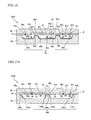
- Fig.11A is a cross-sectional view of a ring or hoop-like shape resonator gyroscope 600 that is MEMS device, an example of another exemplary embodiment.
- Fig 11A is a figure corresponding to Fig. 3 of the first exemplary embodiment.
- Fig 11B is a partial cross-sectional view corresponding to Fig 5E .
- Fig 11C is a partial cross-sectional view corresponding to Fig 5F .
- the configuration of the ring or hoop-like shape resonator gyroscope 600 of the exemplary embodiment is similar to that of the first exemplary embodiment except for the getter film 140.
- the manufacturing methods are similar to those of the first exemplary embodiment except for process steps illustrated in Fig. 11B and Fig. 11C .
- the operational methods are also similar to those of the first exemplary embodiment. Therefore, descriptions of features and processes similar to those of the first exemplary embodiment are omitted herein for brevity.
- the cavities according to this exemplary embodiment have sides extending upwardly, and tapering outwardly, from the bottom surface, and therefore a getter film 140 is formed only on the sides of the cavity and the column-shaped structure 39, and only on a region formed on a surface of a periphery of the lower glass substrate 32 not having a cavity made thereupon, by changing the mask pattern, as illustrated in Fig 11A .
- a getter film region formed on the bottom of the cavity is not formed.
- a getter film region 140b on the sides is continuous with a getter film 140c on a column-shaped structure 39.
- another getter film region 140d on the sides is continuous with the getter film region 140e on a surface of a periphery of the lower glass substrate 32 not having a cavity made thereupon.
- the periphery 12 of the vibrator 10 is connected to a ground potential. Accordingly, the getter film region 140d and getter film region 140e share the ground potential, thereby preventing a floating condition.
- the getter film region 140b and the getter film 140c substantially share the electrical potential applied to the central portion 24, thereby preventing a floating condition.
- the electrical potential is a direct-current electrical potential and therefore stabilizes the electrical potential of the getter film 140 as well.
- the getter film 40 fails to be continuous to the surface of the periphery of the lower glass substrate 32 not having a cavity made thereupon due to a presence of the primary mode sensing electrode 18c.
- the getter film 140 illustrated in Fig.11B and Fig.11C is formed, by utilizing a continuous getter film on the sides of the cavity that is not illustrated, to be continuous with the getter film region 140d illustrated in Fig.11A .
- the configuration that does not form a getter film region on a bottom of the cavity 60 may be also applied to other exemplary embodiments except for the first exemplary embodiment.
- absorption of residual gases after the anodic bonding by the getter film 140 is decreased as compared with that of the first exemplary embodiment, because the getter film region on a bottom of the cavity 60 is not formed.
- the first exemplary embodiment is preferable to the exemplary embodiment.
- the getter film formed on not less than 50% of a total surface area of the cavity is one preferable exemplary embodiment from the viewpoint of absorption of residual gases.
- the getter according to this exemplary embodiment is made of titanium, but the present invention is not limited to this material.
- the getter may include, for example, one or more metals selected from the group consisting of zirconium, vanadium, aluminum, tantalum, tungsten, and molybdenum.
- This exemplary embodiment utilizes a ring or hoop-like shape resonator gyroscope having silicon base material, but the present invention is not limited to this material.
- the base material of the MEMS device can be made of germanium or silicon-germanium.
- the present invention may be implemented for MEMS devices including acceleration sensors, angular velocity sensors, micro mirrors, and RF switches formed inside hermetic chambers.
Landscapes
- Engineering & Computer Science (AREA)
- Microelectronics & Electronic Packaging (AREA)
- Computer Hardware Design (AREA)
- Micromachines (AREA)
- Mechanical Light Control Or Optical Switches (AREA)
Abstract
Description
- The present invention relates to a Micro Electro Mechanical Systems (MEMS) device formed inside a hermetic chamber having a getter film.
- Silicon-based MEMS devices are rapidly progressing in a growing number of technical fields. In recent years, MEMS devices are utilized not only in micro turbines and sensors, but also in communications and medical fields. Getter technology represents a fundamental element of MEMS technology. Getters are important for stabilizing a performance of MEMS devices formed inside hermetic chambers. Improved getter technology is indispensable to an advancement of many fields, especially fields requiring miniaturization in applications such as sensors.
- Conventional getters are formed by vapor deposition on a bottom of a cavity made in a glass substrate. A hermetic chamber is formed, for example, by bonding silicon and glass substrates by anodic bonding. The getter absorbs an amount of oxygen or other residual gases remaining after the anodic bonding, as described in Japanese Published Unexamined Patent Application No.
10-122869 - Japanese Published Unexamined Patent Application No.
10-213441 - Unfortunately, a location of the getter film inside the hermetic chamber may affect various aspects of performance of the MEMS device. For example, in the case where a portion of a getter is too close to an electrode formed on a MEMS device, even though no physical contact is made therebetween, electric noise may transmit from the electrode via the getter film coupled capacitively to an electrode of a sensor or a driver, thereby impairing the operation of the MEMS device.
- Such problems are especially pronounced in the case where a miniature MEMS device is utilized in, for example, a resonator gyroscope chip having a substantially square cross-section occupying 100 mm2 or less when viewed from the front, as illustrated in
Fig. 1 . In particular, the miniaturization of a device requires a smaller volume of hermetic chamber. Gases such as residual gases and gases released into the hermetic chamber during production remain inside the hermetic chamber. The smaller hermetic chamber volume results in stronger influences of these gases on the pressure inside the hermetic chamber. As a result, a detection sensitivity of a MEMS sensor, for example, may be noticeably impaired. Thus, the technical significance of the getter region for miniature MEMS devices is particularly high.
Unfortunately, it is very difficult to form conventional getters that solve the problems recited above while maintaining the required gas absorption capabilities. - The present invention is directed to solve the above recited technical obstacles, thereby greatly contributing to the optimization of the spatial relationship between a MEMS device formed inside a hermetic chamber and a getter useful for maintaining the performance thereof. The inventors focused firstly made a cavity in a substrate to form a hermetic cavity and focused on the depth of the cavity in the case where a getter region is formed on the bottom of the cavity. As a result of various experiments, it became apparent that a technical dilemma exists relating to a position of the getter region and the cavity depth.
- In particular, in the case of shallow cavities, even, for example, in the case where a mask is used to form the getter film only on the bottom of the cavity, the location of the getter film becomes proximal to electrodes of the MEMS device, thereby resulting in electric noise transmitting via the getter film coupled capacitively to electrodes of sensors or drivers. Conversely, technical obstacles exist in the case where the cavity is deep, as described herewith by an example of a conventional MEMS device application.
Fig. 12 is a partial cross-sectional view of a conventional ring or hoop-likeshape resonator gyroscope 700 along the C-C line ofFig. 2 . In the case where a deep cavity is made, a first glance suggests that a mask may be used to successfully form a getter film substantially only on the bottom of adeep cavity 74, but unfortunately this is not practically so. Conventional techniques such as sputtering create agetter film 73 that not only covers the bottom of thecavity 74 but also extends along the sides thereof, as illustrated inFig. 12 . Thus, it is difficult to maintain distances sufficient to prevent effects among members such as thegetter film 73 and the primary mode sensingelectrode 75. As a result, deep cavities do not solve the problems of shallow cavities. Moreover, deep cavities have disadvantages during manufacturing such as longer processing times and poorer process yields. - The inventors performed extensive and diligent research in light of the problems recited above. As a result, a configuration was created, including a getter region formed on a bottom and/or sides of a cavity made in a substrate and a deliberate stabilization of an electrical potential of the getter, thereby completing the present invention.
- One MEMS device according to the present invention includes a movable portion and a fixed portion formed inside a hermetic chamber. The hermetic chamber is formed by a glass substrate having a cavity made therein and a base material of the MEMS device. One or a plurality of getter films are formed inside the hermetic chamber and interconnect therein. A portion of the getter film is connected via the base material of the MEMS device to only one of any one or a plurality of predetermined electrical potentials of the fixed portion and a ground potential of the fixed portion.
- Here, the getter film is not limited to a continuous single entity or one interconnected getter film. For example, getter films may be divided into a plurality of regions. Even in a case where the getter film is divided into a plurality of regions, each getter film connects via the base material of the MEMS device to only one predetermined electrical potential or only a ground potential, respectively. In order words, each of the continuous getter films may not connect simultaneously to two predetermined electrical potentials having a difference therebetween. Likewise, the scope of the present invention includes the case where the getter films are divided into a plurality of regions, each region connects to a predetermined electrical potential (including a ground potential), respectively, and the predetermined electrical potentials differ from one another.
- According to this MEMS device, the getter film is formed inside the hermetic chamber and connected to only one predetermined electrical potential or a ground potential, thereby preventing the potential of the getter film from so-called floating even during the operation of the MEMS device. Therefore, even in the case where the getter film is formed near an electrode of the MEMS device, the electrical potential applied to the getter is stabilized, thereby preventing the transmission of electric noise from the electrode through the getter to an electrode of a sensor or a driver. In addition, the cavity made in the glass substrate for forming the hermetic chamber can be made much shallower than that of conventional art. Therefore, less processing time, simpler manufacturing steps, and greatly reducing manufacturing costs can be achieved.
- Another MEMS device according to the present invention includes a movable portion and a fixed portion formed inside a hermetic chamber. The hermetic chamber is formed by a glass substrate having a cavity made therein and a base material of the MEMS device. A getter film is formed on a bottom and a side surface, or a side surface of the cavity. The getter film extends from the at least one of the bottom surfaces and the side surfaces via a surface of a support of the glass substrate for supporting the MEMS device, contacting to a surface of at least a portion of the fixed portion connecting to only any one or a plurality of predetermined electrical potentials.
- Yet another MEMS device according to the present invention includes a movable portion and a fixed portion formed inside a hermetic chamber. The hermetic chamber is formed by a glass substrate having a cavity made therein and a base material of the MEMS device. A getter film is formed on a bottom and a side surface, or a side surface of the cavity. The getter film on the bottom and/or the side surface of the cavity extends to a surface of at least a portion of the fixed portion and contacts thereto, the fixed portion being connected to only one ground potential.
- According to each of the MEMS devices recited above, the getter film formed inside the hermetic chamber is connected to only one or a plurality of predetermined electrical potentials, thereby preventing the potential of the getter film from floating even during the operation of the MEMS device. Therefore, even in the case where the getter film is formed near each of electrodes of the MEMS device, the electrical potential applied to the getter film is stabilized, thereby preventing the transmission of electric noise from the electrode via the getter to an electrode of a sensor or a driver. In addition, the cavity made in the glass substrate for forming the hermetic chamber can be made much shallower than that of conventional art. Therefore, less processing time, simpler manufacturing steps, and greatly reducing manufacturing costs can be achieved. Connecting the getter film to only a ground potential provides a more stable potential than connecting the getter film to only a predetermined electrical potential other than a ground potential, thereby further reducing electric noise transmitted to the electrodes of the sensors or the drivers, thus providing more favorable characteristics.
- Here, the fixed portion of the present invention may be a portion or an entirety of a non-moving member having a prescribed role in the MEMS device including an electrical effect, a physical effect, or an advantage during a manufacturing process. Likewise, the non-moving member having the prescribed role may in its entirety be the fixed portion, or may include only a portion that is the fixed portion. In all of the aspects of the present invention recited above, favorable absorption of residual gases and gases released into the hermetic chamber is provided by using a getter film material including at least one non-evaporable metal selected from the group consisting of titanium, zirconium, vanadium, aluminum, tantalum, tungsten, and molybdenum.
- According to a MEMS device of the present invention, a getter film is formed inside a hermetic chamber and connected to only one predetermined electrical potential or ground potential, thereby preventing the potential of the getter film from floating even during the operation of the MEMS device. Therefore, even in the case where the getter film is formed near an electrode of the MEMS device, the electrical potential applied to the getter is stabilized, thereby preventing a transmission of electric noise from the electrode through the getter to an electrode of a sensor or a driver. In addition, the cavity made in the glass substrate for forming the hermetic chamber can be made much shallower than that of conventional art. Therefore, less processing time, simpler manufacturing steps, and greatly reducing manufacturing costs can be achieved.
- These objects and other objects and advantages of the present invention will become more apparent upon reading of the following detailed description and the accompanying drawings in which:
-
Fig. 1 is a front view of a MEMS device according to an exemplary embodiment of the present invention; -
Fig. 2 is a partially enlarged view of the A-A quadrant of the MEMS device illustrated inFig. 1 ; -
Fig. 3 is a cross-sectional view along the B-B line ofFig. 1 -
Fig. 4 is an exploded perspective view of a MEMS device including a package according to an exemplary embodiment of the present invention; -
Fig. 5A is a cross-sectional view illustrating a process step for manufacturing the MEMS device according to an exemplary embodiment of the present invention; -
Fig. 5B is a cross-sectional view illustrating a process step for manufacturing the MEMS device according to an exemplary embodiment of the present invention; -
Fig. 5C is a cross-sectional view illustrating a process step for manufacturing the MEMS device according to an exemplary embodiment of the present invention; -
Fig. 5D is a cross-sectional view illustrating a process step for manufacturing the MEMS device according to an exemplary embodiment of the present invention; -
Fig. 5E is a cross-sectional view illustrating a process step for manufacturing the MEMS device according to an exemplary embodiment of the present invention; -
Fig. 5F is a cross-sectional view illustrating a process step for manufacturing the MEMS device according to an exemplary embodiment of the present invention; -
Fig. 6 is a cross-sectional view of a MEMS device according to another exemplary embodiment of the present invention; -
Fig. 7 is a cross-sectional view of a MEMS device according to another exemplary embodiment of the present invention; -
Fig. 8 is a cross-sectional view of a MEMS device according to another exemplary embodiment of the present invention; -
Fig. 9 is a front view of a MEMS device according to another exemplary embodiment of the present invention; -
Fig. 10 is a cross-sectional view of the MEMS device according to another exemplary modification of the present invention; -
Fig. 11A is a cross-sectional view corresponding toFig.3 of the MEMS device according to another exemplary embodiment of the present invention; -
Fig. 11B is a cross-sectional view illustrating a process step for manufacturing the MEMS device according to another exemplary embodiment of the present invention; -
Fig. 11C is a cross-sectional view illustrating a process step for manufacturing the MEMS device according to another exemplary embodiment of the present invention; and -
Fig. 12 is a partial cross-sectional view of a conventional MEMS device. -
- 10: Vibrator
- 12 Periphery
- 14: Ring
- 16, 17a, 17b: Suspensions
- 18a, 18e: Primary mode drive electrode
- 18b, 18f: Secondary mode sensing electrode
- 18c, 18g, 75: Primary mode sensing electrode
- 18d, 18h: Secondary mode drive electrode for nulling the
secondary mode - 24: Central portion
- 26, 27, 28: Trenches
- 30, 71: Upper glass substrates
- 32, 72: Lower glass substrates
- 34, 36a, 36b, 36c, 36d, 36e, 36f, 36g, 36h, 36j, 36k, 36m, 60, 74: Cavities
- 37: Hole
- 38a, 38b, 38c, 38d, 38e, 38f: Electrode pads
- 39 Column-shaped structure
- 40, 40a, 40b, 40c, 40d, 40e, 40f, 40g, 50, 50a, 50b, 50c, 73, 140, 140b, 140c,
- 140d, 140e: Getter films
- 42: Lid
- 44: Resonator gyroscope platform
- 100, 200, 300, 400, 500, 600, 700: Ring or hoop-like shape resonator gyroscope
- Herewith, several exemplary embodiments of the present invention are described with reference to the drawings. In all drawings and descriptions thereof, the same reference numerals are used for similar components unless otherwise noted. Some components of exemplary embodiments are not drawn to scale. Some reference numerals are omitted for better readability in some drawings.
- Structures performing central roles in a MEMS device, i.e., a ring or hoop-like
shape resonator gyroscope 100, according to an exemplary embodiment of the present invention are illustrated in the front view ofFig. 1. Fig. 2 is a partially enlarged view of the A-A quadrant ofFig. 1 .Fig. 3 is a cross-sectional view along the B-B line ofFig. 1 .Fig. 4 is an exploded perspective view of the ring or hoop-likeshape resonator gyroscope 100 according to this exemplary embodiment, including a package. - The MEMS device according to this exemplary embodiment illustrated in
Fig.1 through Fig.4 is the ring or hoop-likeshape resonator gyroscope 100. The ring or hoop-likeshape resonator gyroscope 100 includes: anupper glass substrate 30, havingcavities lower glass substrate 32, having acavity 34 made therein; a silicon vibrator (hereinafter referred to as "vibrator") 10 formed by such techniques as trench etching; and a structure having thevibrator 10 disposed between theupper glass substrate 30 and thelower glass substrate 32, as illustrated inFig. 3 . Here, corresponding faces of theupper glass substrate 30, thelower glass substrate 32, and thevibrator 10 are fused together by anodic bonding, thereby forming a hermetic chamber defined in part by thecavity 34 and thecavities 36a through 36g. - The cavity made in the
lower glass substrate 32 has an annular shape while leaving a column-shapedstructure 39 in a central zone, as illustrated inFig. 4 . Agetter film 40 is formed on a surface of the column-shapedstructure 39, contacts thecentral portion 24 of thevibrator 10, and thereby supports a portion of thevibrator 10. Other portions of thevibrator 10 not supported by the column-shapedstructure 39, such as for example electrodes for trimming thenatural frequency 20a through 20s, are bonded to theupper glass substrate 30 and suspended thereby, as illustrated inFig. 3 . - Holes such as
holes 37 are made in theupper glass substrate 30 to enable wires for operating the ring or hoop-likeshape resonator gyroscope 100 to pass therethrough for connection to members such aselectrode pads upper glass substrate 30, i.e., thecavity 36g, communicates with theholes 37, as illustrated inFig. 3 . In particular, theupper glass substrate 30, thelower glass substrate 32, and thevibrator 10 are bonded together as illustrated inFig. 4 , after which the wires from the each of electrodes is connected to output pins (not illustrated) on aresonator gyroscope platform 44. Then, the ring or hoop-likeshape resonator gyroscope 100 is sealed by resistance welding of alid 42 to theresonator gyroscope platform 44 in a dry nitrogen atmosphere. Sealing the ring or hoop-likeshape resonator gyroscope 100 in this way locks out air, thereby preventing penetration of moisture and other contaminants that may impair the performance thereof. - According to the MEMS device of this exemplary embodiment, the
getter film 40 is formed on the bottom of thelower glass substrate 32, the sides of thelower glass substrate 32, and a surface of thelower glass substrate 32, the surface having no cavity formed thereupon. In particular, thegetter film 40 includes: agetter film region 40a formed on the bottom of thecavity 34; agetter film region 40b formed on sides of the cavity; and agetter film region 40c on a surface of a region of thelower glass substrate 32 having no cavity formed thereupon. The getter film regions are interconnected as illustrated inFig. 3 . According to this exemplary embodiment, a portion of the sides of the cavity includes a side of the column-shapedstructure 39 supporting a portion of thevibrator 10. Furthermore, the getter film according to this exemplary embodiment is a thin titanium film having a thickness of not less than 0.1 µm and not more than 2 µm. - However, according to this exemplary embodiment, a portion of the getter film, i.e., the
getter film region 40c, is formed on a surface of thelower glass substrate 32 having no cavity made thereupon. The formation of thegetter film region 40c thereby results in compressive stresses on thelower glass substrate 32 and thecentral portion 24 of thevibrator 10. Therefore, thecavity 36g provides a recess around the region ofvibrator 10 undergoing compressive stress, i.e., the entire region of thecentral portion 24 as the fixed portion, thereby avoiding bonding with theupper glass substrate 30, as illustrated inFig. 3 . Thecentral portion 24 is allowed thereby to flex upward to relieve stress, thus sufficiently reducing the effects of the compressive stress on thevibrator 10 and providing stable operations thereof. - As described above, a portion of the
getter film 40 according to this exemplary embodiment contacts a surface of thecentral portion 24, i.e., a portion of the fixed portion of thevibrator 10. Thus, thegetter film 40 contacts a portion of thevibrator 10 having a predetermined electrical potential, thereby preventing a floating potential of thegetter 40. In particular, one continuous body is formed, including: tabs remaining from etching 22 defined by atrench 26 cutting through the base material;suspensions 16 likewise defined by thetrench 26 and atrench 28; thecentral portion 24, i.e., fixed ends of thesuspensions 16; and aring 14. In other words, thecentral portion 24 is electrically connected to the tabs remaining from etching 22, thering 14, and thesuspensions 16. During operation of thevibrator 10, a direct current voltage is applied to thering 14 and thesuspensions 16 through thecentral portion 24 by a direct-current power source (not illustrated). Thus, theentire getter film 40, i.e., thegetter film region 40a, thegetter film region 40b, and thegetter film region 40c, substantially share the electrical potential applied to thecentral portion 24, thereby preventing a floating condition. The electrical potential is a direct-current electrical potential and therefore stabilizes the electrical potential of thegetter film 40 as well. - According to this exemplary embodiment, alternating electrical potentials are applied to primary
mode drive electrodes secondary mode electrodes getter film 40 does not contact the surfaces of theelectrodes getter film 40, electric noise from the alternating electrical potential is transmitted to an electrode of a sensor or a driver. Moreover, in the case when thecontinuous getter film 40 according to this exemplary embodiment contacts, for example, more than one fixed portion, all of the fixed portions receive substantially the same electrical potential from a direct-current power source. In the case where a difference in electrical potential exists across thegetter film 40 during operation of thevibrator 10, thegetter film 40 may release heat, thereby impairing the performance of thevibrator 10. In addition, getters often are made of conducting metals, and therefore may result in an electrical short in the case where a getter is connected to electrodes that differ from one electrical potential to another. Such an electrical short may disable the operation of the MEMS device. - According to conventional art, however, a getter film is formed on the bottom of the
cavity 34 formed on thelower glass substrate 32. The getter film functions as a floating electrode, and therefore the cavity must be made to a sufficient depth of, for example, 200 µm or more to avoid electric noise transmitting through a capacitive coupling from an electrode of thevibrator 10 to an electrode of a sensor or a driver. Conversely, for a MEMS device application according to this exemplary embodiment, thecavity 34 may have a depth d1 of 30 µm, as illustrated inFig. 3 , and yet the configuration as recited above prevents the getter film from transmitting electric noise by a capacitive coupling from one electrode to another. In the case of a MEMS device in which the movable portion moves substantially in the same plane as the fixed portion, such as the MEMS device according to this exemplary embodiment, the depth d1 can be not less than 5 µm. In the case of a MEMS device in which the movable portion moves substantially perpendicular to the plane of the fixed portion, it is favorable for the depth d1 to be not less than 10 µm. There is no particular maximum limit to the depth of thecavity 34, but considerations such as minimizing the time to make thecavity 34 and the amount of gases released, considered to be a function of the surface areas of the inner walls of the hermetic chamber, dictate that it is favorable to use a depth d1 of 60 µm or less. Thus, the etching depth can be made much shallower than that of conventional art. Therefore, less processing time and simpler manufacturing steps can be achieved. The cavities in theupper glass substrate 30 may have similar depths as those of thelower glass substrate 32. The depths of the cavities in theupper glass substrate 30 may be the same as the depths of the cavities in the lower glass or reduced further providing that the movement of thevibrator 10 is not impaired. - In addition, noble gases such as argon gas residing inside the hermetic chamber and not absorbed by the getter film are sealed inside the hermetic chamber at pressures not less than 1 Pa and not more than 20 Pa, thereby preventing an extreme vacuum inside the hermetic chamber and providing an appropriate Q factor of the resonator gyroscope. Reducing the depth of the
cavity 34 in thelower glass substrate 32 as recited above allows a much thinner application as compared to that of conventional art, thereby allowing a much thinner glass substrate without compromising the strength of the entire MEMS device. For example, the thickness of a conventional glass substrate is about 600 µm, while the thickness of the same according to this exemplary embodiment is about 450 µm. Thus, compact MEMS devices can be provided. As a result, manufacturing costs can be reduced greatly over those of conventional art. - Herewith, the operation of the ring or hoop-like
shape resonator gyroscope 100 according to this exemplary embodiment is described with reference toFig. 1 through Fig. 3 . As described above, a direct-current electrical potential from a direct-current power source (not illustrated) is applied to thecentral portion 24 of the ring or hoop-likeshape resonator gyroscope 100. An alternating electrical potential from an alternating-current power source (not illustrated) is applied to the primarymode driving electrodes mode sensing electrodes mode sensing electrodes secondary mode natural frequency 20a through 20s. Secondary mode drive electrodes for nulling thesecondary mode natural frequency 20a through 20s are connected to direct-current power sources. Thetrench 28 electrically and physically partitions aperiphery 12 from thering 14 and each of theelectrodes 18a through 18h disposed around the periphery of thering 14. Theperiphery 12 is connected to a ground potential. - First, an alternating electrical potential is applied to the primary
mode drive electrodes ring 14 and the primarymode drive electrodes shape resonator gyroscope 100. The primary vibration mode is detected by the primarymode sensing electrodes mode sensing electrodes natural frequency 20a through 20s, thereby causing a difference in potential between thering 14 and each of theelectrodes 20a through 20s. These differences in potential match the natural frequency of the primary vibration mode to the natural frequency of the secondary vibration mode. Then, an electrical current produced by a change in the electrostatic capacitance corresponding to the applied angular velocity is detected by the secondarymode sensing electrodes secondary mode - Herewith, a method for manufacturing the MEMS device according to this exemplary embodiment is described with reference to
Fig. 5A through Fig. 5F . The description of the manufacturing method refers to the partial cross section of thevibrator 10 along line C-C inFig. 2 . - First,
cavities including cavity 34 andcavities upper glass substrate 30 and thelower glass substrate 32 by a known wet etching process using a glass etching solution. In particular, patterns are formed by known photolithographic methods on theupper glass substrate 30 and thelower glass substrate 32. Then, although etching conditions depend upon the desired depth, the cavities illustrated inFig. 5A and Fig. 5B are made by immersing theupper glass substrate 30 and thelower glass substrate 32 in a 10% hydrofluoric acid solution at 30°C for 5 to 30 minutes. Here, thecavity 36m according to this exemplary embodiment is made in a region to subsequently communicate with one of theholes 37. This cavity is similar to thecavity 36g ofFig. 3 . Etching to define the hermetic chamber is performed to theupper glass substrate 30 from one side, after which theholes 37 are made from the other side by etching or grit blasting. - Then, a silicon substrate S, which forms the base of the
vibrator 10 performing a central role of the MEMS device according to this exemplary embodiment, is bonded to theupper glass substrate 30 by anodic bonding by known conditions such as those discussed in Japanese Published Unexamined Patent Application No.2005-016965 Fig. 5C . - A photoresist mask is formed on the silicon substrate S by known photolithographic methods. Known anisotropic etching technology is then used to make the
trenches vibrator 10 on theupper glass substrate 30, as illustrated inFig. 5D . Examples of etching and related technology include those of other prior patent applications by the applicant of the present invention such as Japanese Published Unexamined Patent Application No.2007-035929 2002-158214 2004-228556 2004-296474 - Known sputtering or vacuum vapor deposition methods are used with a metal mask to form the titanium getter film 40 (40a, 40b, 40c) on surfaces of the
lower glass substrate 32 having a cavity made therein. Here, thegetter film region 40b is formed on sides of the column-shapedstructure 39, and thegetter film region 40c is formed on the surface of the column-shapedstructure 39 having no cavity made thereupon, as illustrated inFig. 5E andFig. 2 . - Then, similarly to the above description, the
vibrator 10 is bonded to thelower glass substrate 32 by anodic bonding using known conditions such as those discussed in Japanese Published Unexamined Patent Application No.2005-016965 electrode pads 38a through 38f are formed as layers of Al, Al alloy, or Au by known sputtering or vacuum vapor deposition methods, as illustrated inFig. 5F . - After the ring or hoop-like
shape resonator gyroscope 100 is manufactured as recited above, holes such as theholes 37 are made to enable wires from electric power supplies (not illustrated) to pass therethrough for connection to members such aselectrode pads 38a through 38f. Finally, the ring or hoop-likeshape resonator gyroscope 100 is sealed as recited above by resistance welding of thelid 42 to theresonator gyroscope platform 44 in a dry nitrogen atmosphere. -
Fig. 6 is a cross-sectional view of another ring or hoop-likeshape resonator gyroscope 200 according to this exemplary embodiment of the present invention. This cross section corresponds toFig. 3 of the first exemplary embodiment. The configuration of the ring or hoop-likeshape resonator gyroscope 200 according to this exemplary embodiment is similar to that according to the first exemplary embodiment except for acavity 60 made in thelower glass substrate 32 and the location of thegetter film 40. The manufacturing methods and operational methods also are similar to those of the first exemplary embodiment. Therefore, descriptions of features and processes similar to those of the first exemplary embodiment are omitted herein for brevity. - The
cavity 60 is made in thelower glass substrate 32 without leaving a column-shaped structure, as illustrated inFig. 6 . However, at least a part of each fixed portion of thevibrator 10 is bonded to theupper glass substrate 30 by anodic bonding, thereby maintaining the shape and preventing gravity from pulling thevibrator 10 down into contact with the bottom of thecavity 60. According to this exemplary embodiment,getter films cavities upper glass substrate 30, and on surfaces of glass substrates not made into cavities. Here, each of thegetter films vibrator 10 having a prescribed direct current voltage, respectively. Thus, each of thegetter films getter films 40d through 40g has a stable electrical potential. - According to this exemplary embodiment, and differing from those of the first exemplary embodiment, each of the
getter films cavities 36a through 36f made in theupper glass substrate 30 and surfaces of glass substrates not having a cavity made thereupon. Such a division of the getter film into distinct regions relieves effects to thevibrator 10 resulting from differences in coefficients of thermal expansion between getter films and glass substrates and residual stresses, and in particular, effects to the thermal characteristics of the zero point output, etc. Moreover, similarly to that of the first exemplary embodiment, thecavity 60 is made to prevent thelower glass substrate 32 from bonding to the entire region in which each fixed portion of thevibrator 10 contacts each of thegetter films 40d through 40g. - According to this exemplary embodiment, even in the case where the depth d2 of the
cavity 60 illustrated inFig. 6 is 20 µm, the getter films do not facilitate capacitive coupling transmitting electric noise among electrodes. In the case of a MEMS device, such as that according to this exemplary embodiment, in which the movable portion moves substantially in the same plane as the fixed portion, the depth d2 can be not less than 5 µm. In the case of a MEMS device in which the movable portion moves substantially perpendicular to the plane of the fixed portion, it is favorable for the depth d2 to be not less than 10 µm. There is no particular maximum limit to the depth of thecavity 60, but considerations such as minimizing the time to form thecavity 60 and the amount of gases released, considered to be a function of the surface areas of the inner walls of the hermetic chamber, dictate that it is favorable to use a depth d2 of 60 µm or less. According to this exemplary embodiment as well, the cavities in theupper glass substrate 30 may have similar depths as those of thelower glass substrate 32. The depths of the cavities in theupper glass substrate 30 can be reduced further providing that the movement of thevibrator 10 is not impaired. - The ability to absorb gases is different for each getter material and formation conditions thereof. Moreover, the amount of gases released varies with factors such as the conditions of the anodic bonding. In some cases therefore, one or more of the
getter films -
Fig. 7 is a cross-sectional view illustrating another ring or hoop-likeshape resonator gyroscope 300 according to this exemplary embodiment. This cross-section corresponds toFig. 3 of the first exemplary embodiment. The configuration of the ring or hoop-likeshape resonator gyroscope 300 of this exemplary embodiment is similar to that of the first exemplary embodiment except for some of the cavities made in theupper glass substrate 30 and the location of agetter film 50. The manufacturing methods and operational methods are similar to those of the first exemplary embodiment. Therefore, descriptions of features and processes similar to those of the first exemplary embodiment are omitted herein for brevity. - The
getter film 50 is formed on the bottom and the sides of a cavity made in thelower glass substrate 32, and on a surface of a periphery of thelower glass substrate 32 not having a cavity made thereupon, thereby surrounding the column-shapedstructure 39, as illustrated inFig. 7 . In particular, thegetter film 50 includes: agetter film region 50a formed on the bottom of the cavity;getter film region 50b formed on the sides of the cavity; and agetter film region 50c formed on a surface of a periphery of thelower glass substrate 32 not having a cavity made thereupon. Thegetter film regions getter film region 50b according to this exemplary embodiment is formed on the side of the column-shapedstructure 39, and therefore does not contact thecentral portion 24. However, thegetter film region 50b formed on the side of the periphery is continuous with thegetter film region 50c on the surface of the lower glass substrate not having a cavity made thereupon, and thegetter film region 50c contacts aperiphery 12 of thevibrator 10. - Here, the
periphery 12 of thevibrator 10 is connected to a ground potential as recited above. Therefore, thegetter film 50 in its entirety shares the ground potential and thus is prevented from having a floating electrical potential. Thus, similar to those according to the first exemplary embodiment, the depths of the cavities may be in the range from 5 µm to 30 µm inclusive without facilitating a transmission of electric noise to the sensors or the driver. Thegetter film region 50c according to this exemplary embodiment is not formed on all regions of theperiphery 12. This configuration thereby increases the anodic bonding regions of thesilicon vibrator 10 and the glass substrate. Thecavity 36a and thecavity 36f made in theupper glass substrate 30 are enlarged to relieve the effects of compressive stress resulting from the presence of thegetter film region 50c. For example, even in the case where a thickness of thegetter film 50 is 2 µm or less, such a configuration for relieving shear forces in this fashion improves the reliability of the MEMS device. - Although according to the first exemplary embodiment recited above, the electrical potential of the
getter film 40 is stabilized by utilizing the column-shapedstructure 39 and thecentral portion 24 of thevibrator 10 supported thereby, the present invention is not limited to such a configuration. For example, regarding the configuration of cavity in thelower glass substrate 32, a column-shaped structure havinggetter film regions shape resonator gyroscope 400 illustrated in the cross-sectional view ofFig. 8 . The tabs remaining from etching 22 receive substantially the same predetermined electrical potential as thecentral portion 24 during operation of thevibrator 10, and therefore similar effects are achieved as those of the first exemplary embodiment. Likewise, similarly to the basis recited above, the effects of the present invention may be achieved in the case where the region of thevibrator 10 supported by the column-shaped structure is, for example, one of the electrodes for trimming thenatural frequency 20a through 20s and has a predetermined electrical potential. - Furthermore, another exemplary embodiment including a partial modification to the configuration of the ring or hoop-shape resonator gyroscope illustrated in
Fig. 8 is described.Fig. 9 is a front view illustrating a MEMS device, i.e., a ring or hoop-likeshape resonator gyroscope 500.Fig. 10 is a partial cross-sectional view of the ring or hoop-likeshape resonator gyroscope 500 along the line B-B ofFig. 9 . According to this exemplary embodiment, a tab remaining from etching supported by a column-shaped structure having thegetter film region 40c formed thereupon is divided by atrench 27 into two tabs remaining frometching regions suspension 17a. Also, another tab remaining from etching is divided by atrench 27 into two tabs remaining frometching regions suspension 17b. Thecavities suspension 17a through the tab remaining frometching 22a and a region from thesuspension 17b through the tab remaining frometching 22d, excluding portions sufficiently distal from thesuspensions upper glass substrate 30. The formation of thecavities suspensions etching getter film region 40c. As a result, the operation of thevibrator 10 is made more stable. More flexure is possible in the case where the entire regions of the tabs remaining frometching upper glass substrate 30. However, providing that the flexures of the tabs remaining frometching etching Fig. 10 . Moreover, thesuspensions - Furthermore, in each of the exemplary embodiments recited above, a ring or hoop-like shape resonator gyroscope is discussed as one examples of a MEMS device, but implementation of the present invention to MEMS devices is not limited to these applications. The present invention may be implemented for other MEMS devices that also can be favorably formed inside a hermetic chamber. In particular, micro mirrors and radio frequency (RF) switches are typical examples of MEMS devices to which the present invention may be implemented.
- Still Furthermore, in each of the exemplary embodiments recited above, getter films are formed on sides as well as bottoms of the cavities, but the present invention is not limited to such configurations. For example, regarding an inward of a cavity, the cavities according to this exemplary embodiment have sides extending upwardly, and tapering outwardly, from the bottom surface, and therefore a getter film may be formed only on the sides thereon by changing the mask pattern. Accordingly, the getter film connects via a base material of the MEMS device from the sides of the cavity to only one of any one of predetermined electrical potentials of the fixed portion and a ground potential of the fixed portion of the MEMS device.
- For example,
Fig.11A is a cross-sectional view of a ring or hoop-likeshape resonator gyroscope 600 that is MEMS device, an example of another exemplary embodiment. Furthermore,Fig 11A is a figure corresponding toFig. 3 of the first exemplary embodiment. Yet furthermore,Fig 11B is a partial cross-sectional view corresponding toFig 5E . Still furthermore,Fig 11C is a partial cross-sectional view corresponding toFig 5F . The configuration of the ring or hoop-likeshape resonator gyroscope 600 of the exemplary embodiment is similar to that of the first exemplary embodiment except for thegetter film 140. Furthermore, the manufacturing methods are similar to those of the first exemplary embodiment except for process steps illustrated inFig. 11B and Fig. 11C . Yet furthermore, the operational methods are also similar to those of the first exemplary embodiment. Therefore, descriptions of features and processes similar to those of the first exemplary embodiment are omitted herein for brevity. - The cavities according to this exemplary embodiment have sides extending upwardly, and tapering outwardly, from the bottom surface, and therefore a
getter film 140 is formed only on the sides of the cavity and the column-shapedstructure 39, and only on a region formed on a surface of a periphery of thelower glass substrate 32 not having a cavity made thereupon, by changing the mask pattern, as illustrated inFig 11A . InFig 11A , a getter film region formed on the bottom of the cavity is not formed. However, agetter film region 140b on the sides is continuous with agetter film 140c on a column-shapedstructure 39. Furthermore, anothergetter film region 140d on the sides is continuous with thegetter film region 140e on a surface of a periphery of thelower glass substrate 32 not having a cavity made thereupon. - The
periphery 12 of thevibrator 10 is connected to a ground potential. Accordingly, thegetter film region 140d andgetter film region 140e share the ground potential, thereby preventing a floating condition. On the other hand, similarly to that of the first exemplary embodiment, thegetter film region 140b and thegetter film 140c substantially share the electrical potential applied to thecentral portion 24, thereby preventing a floating condition. The electrical potential is a direct-current electrical potential and therefore stabilizes the electrical potential of thegetter film 140 as well. InFig.11B and Fig.11C , thegetter film 40 fails to be continuous to the surface of the periphery of thelower glass substrate 32 not having a cavity made thereupon due to a presence of the primarymode sensing electrode 18c. Accordingly, thegetter film 140 illustrated inFig.11B and Fig.11C is formed, by utilizing a continuous getter film on the sides of the cavity that is not illustrated, to be continuous with thegetter film region 140d illustrated inFig.11A . - As described above, regarding an inward of a cavity, even when the getter film 140 (140b, 140d) is formed only on the sides thereon, an effect of the same quality as that of the present invention is obtained by getting a stability of the electrical potential of the
getter film 140. In addition, the configuration that does not form a getter film region on a bottom of thecavity 60 may be also applied to other exemplary embodiments except for the first exemplary embodiment. Moreover, in the exemplary embodiments, absorption of residual gases after the anodic bonding by thegetter film 140 is decreased as compared with that of the first exemplary embodiment, because the getter film region on a bottom of thecavity 60 is not formed. Accordingly, from the viewpoint of absorption of residual gases, the first exemplary embodiment is preferable to the exemplary embodiment. Concretely, as illustrated in the first exemplary embodiment, the getter film formed on not less than 50% of a total surface area of the cavity is one preferable exemplary embodiment from the viewpoint of absorption of residual gases. - Still furthermore, in each of the exemplary embodiments recited above, the getter according to this exemplary embodiment is made of titanium, but the present invention is not limited to this material. The getter may include, for example, one or more metals selected from the group consisting of zirconium, vanadium, aluminum, tantalum, tungsten, and molybdenum. This exemplary embodiment utilizes a ring or hoop-like shape resonator gyroscope having silicon base material, but the present invention is not limited to this material. For example, the base material of the MEMS device can be made of germanium or silicon-germanium. As recited above, modifications within the scope of the present invention are included also in the scope of the patent claims.
- The present invention may be implemented for MEMS devices including acceleration sensors, angular velocity sensors, micro mirrors, and RF switches formed inside hermetic chambers.
Claims (8)
- A MEMS device comprising a movable portion and a fixed portion, characterized in that:the movable portion and the fixed portion are formed inside a hermetic chamber,the hermetic chamber is formed by a glass substrate having a cavity made therein and a base material of the MEMS device; anda portion of one or plurality of continuous getter films formed inside the hermetic chamber connects via the base material of the MEMS device to only one of any one or a plurality of predetermined electrical potentials of the fixed portion and a ground potential of the fixed portion.
- A MEMS device comprising a movable portion and a fixed portion,
characterized in that:the movable portion and the fixed portion are formed inside a hermetic chamber,the hermetic chamber is formed by a glass substrate having a cavity made therein and a base material of the MEMS device; anda getter film is formed on a bottom surface and a side surface, or a side surface of the cavity, the getter film extending from at least one of a bottom surface and a side surface via a surface of a support of the glass substrate supporting the MEMS device, contacting to a surface of at least a portion of the fixed portion connecting to only any one or a plurality of predetermined electrical potentials. - A MEMS device comprising a movable portion and a fixed portion, characterized in that:the movable portion and the fixed portion are formed inside a hermetic chamber,the hermetic chamber is formed by a glass substrate having a cavity made therein and a base material of the MEMS device; anda getter film is formed on a bottom surface and a side surface, or a side surface of the cavity, the getter film extending from at least one of a bottom surface and a side surface, contacting to a surface of at least a portion of the fixed portion connecting to only a ground potential.
- The MEMS device according to claim 1, wherein the getter film is formed on not less than 50% of a total surface area of the cavity.
- The MEMS device according to claim 1, wherein a distance from a surface of the MEMS device to a bottom of the cavity is not less than 5 µm and not more than 60 µm.
- The MEMS device according to claim 2 or claim 3, wherein:at least the fixed portions of the MEMS device contacting the getter film are not bonded to the glass substrate.
- The MEMS device according to claim 2 or claim 3, wherein the fixed portion contacting the getter film connects via an elastic structure to the fixed portion having no contact with the getter film, and is not bonded to the glass substrate continuously from the elastic structure through the fixed portion contacting the getter film.
- The MEMS device according to claim 2 or claim 3, wherein the getter film comprises at least one type of metal selected from the group consisting of titanium, zirconium, vanadium, aluminum, tantalum, tungsten, and molybdenum.
Applications Claiming Priority (2)
| Application Number | Priority Date | Filing Date | Title |
|---|---|---|---|
| JP2007168966 | 2007-06-27 | ||
| JP2008155682A JP2009028891A (en) | 2007-06-27 | 2008-06-13 | MEMS device formed in sealed space having getter film |
Publications (2)
| Publication Number | Publication Date |
|---|---|
| EP2008966A2 true EP2008966A2 (en) | 2008-12-31 |
| EP2008966A3 EP2008966A3 (en) | 2013-06-12 |
Family
ID=39828275
Family Applications (1)
| Application Number | Title | Priority Date | Filing Date |
|---|---|---|---|
| EP08252173.3A Withdrawn EP2008966A3 (en) | 2007-06-27 | 2008-06-24 | MEMS device formed inside hermetic chamber having getter film |
Country Status (2)
| Country | Link |
|---|---|
| US (1) | US7696622B2 (en) |
| EP (1) | EP2008966A3 (en) |
Cited By (4)
| Publication number | Priority date | Publication date | Assignee | Title |
|---|---|---|---|---|
| WO2010092842A1 (en) * | 2009-02-11 | 2010-08-19 | 住友精密工業株式会社 | Vibratory gyro using piezoelectric film and method for manufacturing thereof |
| FR2950877A1 (en) * | 2009-10-07 | 2011-04-08 | Commissariat Energie Atomique | CAVITY STRUCTURE COMPRISING A BONDING INTERFACE BASED ON MATERIAL GETTER |
| CN105307974A (en) * | 2013-06-12 | 2016-02-03 | 特罗尼克斯微系统有限公司 | MEMS device with getter layer |
| CN114505629A (en) * | 2022-03-15 | 2022-05-17 | 哈尔滨工业大学 | Electrode substrate fixing device for welding hemispherical harmonic oscillator and electrode substrate |
Families Citing this family (8)
| Publication number | Priority date | Publication date | Assignee | Title |
|---|---|---|---|---|
| TWI358235B (en) * | 2007-12-14 | 2012-02-11 | Ind Tech Res Inst | Sensing membrane and micro-electro-mechanical syst |
| WO2011083158A2 (en) * | 2010-01-11 | 2011-07-14 | Elmos Semiconductor Ag | Micro-electromechanical semiconductor component |
| US8748206B2 (en) * | 2010-11-23 | 2014-06-10 | Honeywell International Inc. | Systems and methods for a four-layer chip-scale MEMS device |
| US9171964B2 (en) | 2010-11-23 | 2015-10-27 | Honeywell International Inc. | Systems and methods for a three-layer chip-scale MEMS device |
| US8569090B2 (en) * | 2010-12-03 | 2013-10-29 | Babak Taheri | Wafer level structures and methods for fabricating and packaging MEMS |
| US8395229B2 (en) | 2011-03-11 | 2013-03-12 | Institut National D'optique | MEMS-based getter microdevice |
| NO2944700T3 (en) | 2013-07-11 | 2018-03-17 | ||
| FR3008965B1 (en) * | 2013-07-26 | 2017-03-03 | Commissariat Energie Atomique | ENCAPSULATION STRUCTURE COMPRISING A MECHANICALLY REINFORCED HOOD AND GETTER EFFECT |
Citations (7)
| Publication number | Priority date | Publication date | Assignee | Title |
|---|---|---|---|---|
| JPH10122869A (en) | 1996-10-22 | 1998-05-15 | Murata Mfg Co Ltd | External force detector and its manufacture |
| JPH10213441A (en) | 1997-01-29 | 1998-08-11 | Murata Mfg Co Ltd | External force detector and its manufacture |
| JP2002158214A (en) | 2000-11-21 | 2002-05-31 | Sumitomo Precision Prod Co Ltd | Method and apparatus for anisotropic etching of silicon |
| JP2004228556A (en) | 2002-11-29 | 2004-08-12 | Sumitomo Precision Prod Co Ltd | Laminated member, method of manufacturing the same, and apparatus for manufacturing the same |
| JP2004296474A (en) | 2003-03-25 | 2004-10-21 | Sumitomo Precision Prod Co Ltd | Method and apparatus for etching silicon substrate |
| JP2005016965A (en) | 2003-06-23 | 2005-01-20 | Sumitomo Precision Prod Co Ltd | Package and manufacturing method thereof, and vibration gyro and manufacturing method thereof |
| JP2007035929A (en) | 2005-07-27 | 2007-02-08 | Sumitomo Precision Prod Co Ltd | Etching method and etching apparatus |
Family Cites Families (1)
| Publication number | Priority date | Publication date | Assignee | Title |
|---|---|---|---|---|
| US7204737B2 (en) * | 2004-09-23 | 2007-04-17 | Temic Automotive Of North America, Inc. | Hermetically sealed microdevice with getter shield |
-
2008
- 2008-06-24 EP EP08252173.3A patent/EP2008966A3/en not_active Withdrawn
- 2008-06-26 US US12/147,197 patent/US7696622B2/en not_active Expired - Fee Related
Patent Citations (7)
| Publication number | Priority date | Publication date | Assignee | Title |
|---|---|---|---|---|
| JPH10122869A (en) | 1996-10-22 | 1998-05-15 | Murata Mfg Co Ltd | External force detector and its manufacture |
| JPH10213441A (en) | 1997-01-29 | 1998-08-11 | Murata Mfg Co Ltd | External force detector and its manufacture |
| JP2002158214A (en) | 2000-11-21 | 2002-05-31 | Sumitomo Precision Prod Co Ltd | Method and apparatus for anisotropic etching of silicon |
| JP2004228556A (en) | 2002-11-29 | 2004-08-12 | Sumitomo Precision Prod Co Ltd | Laminated member, method of manufacturing the same, and apparatus for manufacturing the same |
| JP2004296474A (en) | 2003-03-25 | 2004-10-21 | Sumitomo Precision Prod Co Ltd | Method and apparatus for etching silicon substrate |
| JP2005016965A (en) | 2003-06-23 | 2005-01-20 | Sumitomo Precision Prod Co Ltd | Package and manufacturing method thereof, and vibration gyro and manufacturing method thereof |
| JP2007035929A (en) | 2005-07-27 | 2007-02-08 | Sumitomo Precision Prod Co Ltd | Etching method and etching apparatus |
Cited By (10)
| Publication number | Priority date | Publication date | Assignee | Title |
|---|---|---|---|---|
| WO2010092842A1 (en) * | 2009-02-11 | 2010-08-19 | 住友精密工業株式会社 | Vibratory gyro using piezoelectric film and method for manufacturing thereof |
| JP2010210605A (en) * | 2009-02-11 | 2010-09-24 | Sumitomo Precision Prod Co Ltd | Vibratory gyro using piezoelectric film and method for manufacturing the same |
| US9151612B2 (en) | 2009-02-11 | 2015-10-06 | Sumitomo Precision Products Co., Ltd. | Vibrating gyroscope including piezoelectric film sandwiched between metallic film layers |
| FR2950877A1 (en) * | 2009-10-07 | 2011-04-08 | Commissariat Energie Atomique | CAVITY STRUCTURE COMPRISING A BONDING INTERFACE BASED ON MATERIAL GETTER |
| EP2308797A3 (en) * | 2009-10-07 | 2011-04-20 | Commissariat à l'Énergie Atomique et aux Énergies Alternatives | Structure with a cavity comprising a bonding interface made from a getter material |
| US8399299B2 (en) | 2009-10-07 | 2013-03-19 | Commissariat A L'energie Atomique Et Aux Energies Alternatives | Cavity structure comprising an adhesion interface composed of getter material |
| CN105307974A (en) * | 2013-06-12 | 2016-02-03 | 特罗尼克斯微系统有限公司 | MEMS device with getter layer |
| EP2813465B1 (en) * | 2013-06-12 | 2020-01-15 | Tronic's Microsystems | MEMS device with getter layer |
| CN114505629A (en) * | 2022-03-15 | 2022-05-17 | 哈尔滨工业大学 | Electrode substrate fixing device for welding hemispherical harmonic oscillator and electrode substrate |
| CN114505629B (en) * | 2022-03-15 | 2022-12-06 | 哈尔滨工业大学 | Electrode substrate fixing device for welding hemispherical harmonic oscillator and electrode substrate |
Also Published As
| Publication number | Publication date |
|---|---|
| US20090001565A1 (en) | 2009-01-01 |
| US7696622B2 (en) | 2010-04-13 |
| EP2008966A3 (en) | 2013-06-12 |
Similar Documents
| Publication | Publication Date | Title |
|---|---|---|
| US7696622B2 (en) | MEMS device formed inside hermetic chamber having getter film | |
| US7748277B2 (en) | Hermetic chamber with electrical feedthroughs | |
| US7647836B2 (en) | Hermetic chamber with electrical feedthroughs | |
| US6736008B2 (en) | Inertia force sensor | |
| US8096187B2 (en) | Pressure sensor element and pressure sensor | |
| JP2006519707A (en) | System and method for electrical feedthrough embedded in a glass-silicon MEMS process | |
| EP1920229B1 (en) | Pressure sensors and methods of making the same | |
| EP2810915B1 (en) | Capacitive sensing structure with embedded acoustic channels | |
| WO2007061841A2 (en) | Capacitor electrode formed on surface of integrated circuit chip | |
| CA2652060A1 (en) | Hermetic chamber with electrical feedthroughs | |
| EP2460763A2 (en) | Wafer level packaging process for MEMS devices | |
| KR100316774B1 (en) | Method for fabricating a micro inertia sensor | |
| KR20030027950A (en) | Silicon device | |
| US6430999B2 (en) | Semiconductor physical quantity sensor including frame-shaped beam surrounded by groove | |
| CN111551161A (en) | MEMS vibrating gyroscope structure and manufacturing method thereof | |
| JP2009028891A (en) | MEMS device formed in sealed space having getter film | |
| KR20040101048A (en) | Capacitance-type dynamic-quantity sensor and manufacturing method therefor | |
| US8329491B2 (en) | Mechanical quantity sensor and method of manufacturing the same | |
| JP2009006428A (en) | MEMS device having getter film formed in sealed space | |
| JPH11326366A (en) | Semiconductor electronic component device and method of manufacturing the same | |
| JP2000022170A (en) | Electronic component and manufacture thereof | |
| EP2435357B1 (en) | Method of accurately spacing z-axis electrode | |
| CN117550546A (en) | Chip preparation method and chip | |
| KR100506073B1 (en) | A vacuum packaged microgyroscope and a fabricating method thereof | |
| JP4883688B2 (en) | Vacuum package, electronic device, and manufacturing method of vacuum package |
Legal Events
| Date | Code | Title | Description |
|---|---|---|---|
| PUAI | Public reference made under article 153(3) epc to a published international application that has entered the european phase |
Free format text: ORIGINAL CODE: 0009012 |
|
| AK | Designated contracting states |
Kind code of ref document: A2 Designated state(s): AT BE BG CH CY CZ DE DK EE ES FI FR GB GR HR HU IE IS IT LI LT LU LV MC MT NL NO PL PT RO SE SI SK TR |
|
| AX | Request for extension of the european patent |
Extension state: AL BA MK RS |
|
| PUAL | Search report despatched |
Free format text: ORIGINAL CODE: 0009013 |
|
| AK | Designated contracting states |
Kind code of ref document: A3 Designated state(s): AT BE BG CH CY CZ DE DK EE ES FI FR GB GR HR HU IE IS IT LI LT LU LV MC MT NL NO PL PT RO SE SI SK TR |
|
| AX | Request for extension of the european patent |
Extension state: AL BA MK RS |
|
| RIC1 | Information provided on ipc code assigned before grant |
Ipc: B81B 7/00 20060101AFI20130503BHEP |
|
| AKY | No designation fees paid | ||
| REG | Reference to a national code |
Ref country code: DE Ref legal event code: R108 |
|
| REG | Reference to a national code |
Ref country code: DE Ref legal event code: R108 Effective date: 20140219 |
|
| STAA | Information on the status of an ep patent application or granted ep patent |
Free format text: STATUS: THE APPLICATION IS DEEMED TO BE WITHDRAWN |
|
| 18D | Application deemed to be withdrawn |
Effective date: 20131213 |