EP2007178B1 - Electronic device with at least one electric connected element and method for producing a connected element - Google Patents
Electronic device with at least one electric connected element and method for producing a connected element Download PDFInfo
- Publication number
- EP2007178B1 EP2007178B1 EP08104210.3A EP08104210A EP2007178B1 EP 2007178 B1 EP2007178 B1 EP 2007178B1 EP 08104210 A EP08104210 A EP 08104210A EP 2007178 B1 EP2007178 B1 EP 2007178B1
- Authority
- EP
- European Patent Office
- Prior art keywords
- collar
- substrate
- housing
- base plate
- connection element
- Prior art date
- Legal status (The legal status is an assumption and is not a legal conclusion. Google has not performed a legal analysis and makes no representation as to the accuracy of the status listed.)
- Expired - Fee Related
Links
Images

Classifications
-
- H—ELECTRICITY
- H05—ELECTRIC TECHNIQUES NOT OTHERWISE PROVIDED FOR
- H05K—PRINTED CIRCUITS; CASINGS OR CONSTRUCTIONAL DETAILS OF ELECTRIC APPARATUS; MANUFACTURE OF ASSEMBLAGES OF ELECTRICAL COMPONENTS
- H05K3/00—Apparatus or processes for manufacturing printed circuits
- H05K3/40—Forming printed elements for providing electric connections to or between printed circuits
- H05K3/4038—Through-connections; Vertical interconnect access [VIA] connections
- H05K3/4046—Through-connections; Vertical interconnect access [VIA] connections using auxiliary conductive elements, e.g. metallic spheres, eyelets, pieces of wire
-
- H—ELECTRICITY
- H05—ELECTRIC TECHNIQUES NOT OTHERWISE PROVIDED FOR
- H05K—PRINTED CIRCUITS; CASINGS OR CONSTRUCTIONAL DETAILS OF ELECTRIC APPARATUS; MANUFACTURE OF ASSEMBLAGES OF ELECTRICAL COMPONENTS
- H05K3/00—Apparatus or processes for manufacturing printed circuits
- H05K3/40—Forming printed elements for providing electric connections to or between printed circuits
- H05K3/4038—Through-connections; Vertical interconnect access [VIA] connections
- H05K3/4084—Through-connections; Vertical interconnect access [VIA] connections by deforming at least one of the conductive layers
-
- H—ELECTRICITY
- H05—ELECTRIC TECHNIQUES NOT OTHERWISE PROVIDED FOR
- H05K—PRINTED CIRCUITS; CASINGS OR CONSTRUCTIONAL DETAILS OF ELECTRIC APPARATUS; MANUFACTURE OF ASSEMBLAGES OF ELECTRICAL COMPONENTS
- H05K2201/00—Indexing scheme relating to printed circuits covered by H05K1/00
- H05K2201/10—Details of components or other objects attached to or integrated in a printed circuit board
- H05K2201/10227—Other objects, e.g. metallic pieces
- H05K2201/10401—Eyelets, i.e. rings inserted into a hole through a circuit board
Definitions
- the invention relates to an electronic device with at least one connecting device having at least one electrical connecting element.
- the invention further relates to a method for producing a connection element of an electronic device.
- Such an electronic device is known, for example, as a control device of a vehicle component of a motor vehicle.
- the control unit has a housing, a circuit arrangement arranged in the housing and a connection device designed as a male connector for making electrical contact with the device, in particular the circuit arrangement.
- the male connector is soldered or pressed onto a circuit carrier of the controller and consists mostly of an arrangement of a plurality of contact plugs in the form of a connector strip, which is surrounded by a contact plug superior protective collar.
- the housing of the controller has a contour of the male connector adapted opening through which this protrudes with its protective collar.
- On the connector strip a device plug is arranged with appropriately arranged as a socket strip contact sockets on the male connector for electrical contacting of the control unit in the motor vehicle.
- DE 14 65 852 discloses a method of making metal clad circuit boards with plated holes. It is envisaged that an exposed metal foil of the lamination is mechanically fed into a hole in the circuit board.
- connection element has an embossed collar of electrically conductive material, in particular metal, introduced into a substrate of the device by joining, which forms at least part of an insertion opening.
- a collar is preferably made of a sheet metal stamped collar.
- the connecting element with the embossed collar has, in particular, a preferably circular base plate with a centrally formed opening, wherein a collar extends perpendicular to the base plate on one side of the base plate at the edge of the aperture.
- the substrate is formed as a plastic part of the device.
- the collar has at its end facing away from the base plate a projection which is formed as a collar surrounding the circumference circumferentially, so that there is a groove between the base plate and the web.
- the collar is pressed into the substrate for the production of the connection element.
- an undercut structure is formed on the collar, which holds the inserted into the substrate stamped collar in the solid material or in a recess of a substrate. If the collar is pressed into solid material of the substrate, the recess is created in a second step, for example by drilling out of the substrate, in the inner region of the collar, whereby the insertion opening is formed.
- the connection element is pressed with the collar directly into a recess, this forms together with the collar the insertion without further processing steps.
- the connection element is an electrical connection element which is in particular contacted with a circuit arrangement of the electrical device.
- the substrate is designed as a plastic part of the device.
- the joining of a stamped collar with a plastic part is known as "collar joining".
- the plastic of the plastic part need not be heated.
- the plastic part is formed as an injection-molded plastic part.
- the pressing (joining) of the collar takes place in particular only after the injection molding process and is thus a so-called PMA process (PMA: Post Molding Assembly).
- the substrate forms or co-forms a housing.
- the connection element is formed with the stamped collar directly on the housing of the device.
- the substrate forms a circuit carrier having at least one conductor track.
- the circuit carrier is for example a printed circuit board.
- the circuit carrier is preferably designed as an injection-molded circuit carrier (MID: Molded Interconnect Device). By means of the MID technology, metallic conductor tracks are applied to injection-molded plastic parts.
- the circuit carrier is, in particular, a circuit carrier forming or forming the housing.
- the conductor track is formed on an inner and / or outer side of the housing, preferably on the inside of the housing.
- the collar is a conductor electrically contacting the collar.
- the collar is in particular introduced into a recess in the region of the conductor track so that the collar bushing electrically contacts the conductor track during the joining process.
- the substrate has a via.
- a via is a plated-through breakthrough in the circuit carrier, which electrically connects the upper side of the circuit carrier to its underside.
- the recess is formed as a via.
- connection element is preferably located in the protruding part of the circuit carrier, so that it can be contacted from the outside, while the circuit arrangement is formed in particular on a part of the circuit carrier, which is surrounded by the housing.
- the device is designed as a control unit of a vehicle component of a motor vehicle.
- controllers are, for example, as engine control units an internal combustion engine or transmission control units of a transmission of the motor vehicle.
- connection element for an electronic device in particular a device mentioned above, is characterized in that a connecting element forming, embossed collar of electrically conductive material, in particular metal, is introduced by joining in a substrate of the device, wherein the Collar in solid material of the substrate is introduced and then an extending into the interior of the collar insertion is created.
- the substrate is preferably a plastic part, in particular an injection-molded plastic part of the device.
- the collar of the connecting element has been created with advantage before the joining process by stamping a metal sheet.
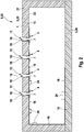
- the FIG. 1 shows in a sectional view a section of a substrate 1 of a in the Figures 2 and 3
- the substrate 1 is a plastic part 3 of the electronic device 2 and is preferably made of injection-molded plastic.
- two partially illustrated connection elements 4 are formed in the in FIG. 1 shown portion of the substrate 1, two partially illustrated connection elements 4 are formed.
- the connection elements 4 are made of metal, preferably sheet metal.
- the section shows the connection between the connecting elements 4 and the substrate 1 which has been created by a joining process FIG. 3
- completely shown connection elements 4 have a base plate 5 with an opening 6 formed in the middle of the base plate 5.
- the opening 6 is circumferentially surrounded in each case by a collar 7 which extends completely vertically away from the base plate 5 from.
- the collar 7 has on its outer side 8 in the region of an end 9 facing away from the base plate 5 a projection 10 which is designed as a collar 7 surrounding the collar 11 in its entirety. Between the base plate 5 and the web 11 results in a groove 12, wherein the web 11 and the groove 12 forms a rear handle structure with the plastic material of the substrate 1 is a rear handle.
- the respective collar 7 forms part of an insertion opening 13 of the associated connection element 4. In the insertion openings 13 of the connection elements 4, not shown male elements of a plug for electrical contact can be inserted.
- the substrate 1 is designed as a circuit carrier 14 and has its in FIG. 1 visible top 15 two tracks 16 on.
- the conductor tracks 16 are arranged parallel to one another and perpendicular to the in the FIG. 1 shown cutting edge.
- the interconnects 16 extend in the region of the cut edge up to the collar 7 of the connection elements 4.
- Each of the connection elements 4 contact the interconnect 16 assigned to it with its collar 7 and a part of its base plate 5 covering the respective interconnect.
- the connecting elements 4 are alternatively created in two ways: Either by the fact that the connecting element 4 co-forming, embossed collar 7 made of metal is introduced by joining in the substrate 1 of the device 2, wherein the collar 7 for forming an insertion opening 13 in a recess 17th of Substrate 1 is introduced.
- the recess 17 is created in a first step and subsequently the collar 7 is introduced into the recess 17 by joining (pressing in).
- the collar 7 is introduced into solid material of the substrate 1 and then the insertion opening 13 extending into the interior of the collar 7 is created.
- the connection element 4 is inserted with its collar 7 in the solid material of the plastic part 2 by pressing and then a recess 17, for example by drilling created.
- the recess 17, such as in FIG. 1 be designed as a breakthrough 18.
- a breakthrough 18 created prior to insertion of the collar 7 can be considered as an in FIG. 2 Shown via 19 may be formed, in which the inside of the opening 18 is coated with conductive material.
- the collar 7 can also be formed on the underside 20 or one collar 7 on the upper and / or lower side 15, 20 for forming the connecting element 4.
- the FIG. 2 shows a sectional view through a housing 21 of a designed as a control unit 22 of a vehicle component of a motor vehicle electronic device 2. At least parts of the housing 21 are formed as a substrate 1. One of the sides 15, 20 of this substrate 1 forms an inner side 23 of the housing 21. On this inner side 23, electronic components 24 of at least one circuit arrangement are arranged.
- the housing 21 of FIG. 2 consists for example of two plastic parts 3, which are formed as a housing cover 25 and housing bottom 26.
- the housing cover 25 has a plurality of connection elements 4, four of which in the sectional view of FIG. 2 are shown and each have one inserted from the inside 23 forth in a trained as Via 19 opening 18 collar 7.
- connecting elements 4 are pressed with their collar 7 from the outside.
- the connecting elements 4 are electrically connected via their collar 7 and the via 19 with the conductor tracks 16 of the circuit substrate 14 and allow contacting of the circuit arrangement in the interior of the housing 21 via the connection elements 4 with introduced into the connection elements 4 pins of a connector, not shown.
- electronic device 2 forms the housing 21, the circuit substrate 14 itself on its inner side 23rd out.
- the housing cover 25 and the housing bottom 26 are each a substrate made of plastic, on the conductor tracks 16 are created by means of MID technology. In order to protect the conductor tracks 16 and the electronic components 24 from external influences, these are arranged within the housing 21.
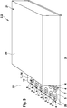
- FIG. 3 shows a schematic representation of a housing 21 of a likewise designed as a control unit 22 electronic device 2.
- the in FIG. 3 Housing 21 shown also consists of a housing cover 25 and a housing bottom 26, wherein the housing bottom 26 is formed as a substrate 1.
- the substrate 1 designed as a circuit carrier 14 protrudes out of the housing 21 in regions.
- the substrate 1 is simultaneously formed as a housing bottom 26, alternatively, the circuit substrate 14 is not part of the housing 21 and protrudes with another area of the housing 21 out.
- a plurality of connection elements 4 are contacted via printed conductors 16, not shown, with a circuit arrangement, also not shown in the housing 21.
Description
Die Erfindung betrifft ein elektronisches Gerät mit mindestens einer mindestens ein elektrisches Anschlusselement aufweisenden Anschlusseinrichtung.The invention relates to an electronic device with at least one connecting device having at least one electrical connecting element.
Die Erfindung betrifft ferner ein Verfahren zur Herstellung eines Anschlusselements eines elektronischen Geräts.The invention further relates to a method for producing a connection element of an electronic device.
Ein derartiges elektronisches Gerät ist zum Beispiel als ein Steuergerät einer Fahrzeugkomponente eines Kraftfahrzeugs bekannt. Das Steuergerät weist ein Gehäuse, eine im Gehäuse angeordnete Schaltungsanordnung und eine als Messerleiste ausgebildete Anschlusseinrichtung zur elektrischen Kontaktierung des Geräts, insbesondere der Schaltungsanordnung, auf. Die Messerleiste ist auf einem Schaltungsträger des Steuergeräts eingelötet oder eingepresst und besteht zumeist aus einer Anordnung von mehreren Kontaktsteckern in Form einer Steckerleiste, die von einem die Kontaktstecker überragenden Schutzkragen umgeben ist. Das Gehäuse des Steuergeräts hat eine der Kontur der Messerleiste angepasste Öffnung, durch die diese mit ihrem Schutzkragen hinausragt. Auf die Steckerleiste wird ein Gerätestecker mit entsprechend als Buchsenleiste angeordneten Kontaktbuchsen auf die Messerleiste zur elektrischen Kontaktierung des Steuergeräts im Kraftfahrzeugs aufgesteckt. Um die im Inneren des Gehäuses befindliche Schaltungsanordnung vor von außen eindringender Feuchtigkeit und Schmutz zu schützen, wird zwischen dem Schutzkragen der Messerleiste und dem Gehäuse des Steuergeräts eine Dichtung eingebracht.
Zum einfachen und kostengünstigen Aufbau des elektronischen Geräts ist vorgesehen, dass das Anschlusselement einen in ein Substrat des Geräts durch Fügen eingebrachten geprägten Kragen aus elektrisch leitfähigem Material, insbesondere Metall, aufweist, der zumindest einen Teil einer Einstecköffnung bildet. Ein derartiger Kragen ist vorzugsweise aus einem Metallblech hergestellter stanzgeprägter Kragen. Das Anschlusselement mit dem geprägten Kragen weist insbesondere eine vorzugsweise kreisförmige Grundplatte mit einem mittig ausgebildeten Durchbruch auf, wobei sich am Rand des Durchbruchs auf einer Seite der Grundplatte ein Kragen senkrecht zur Grundplatte erstreckt. Das Substrat ist als Kunststoffteil des Geräts ausgebildet.For simple and cost-effective construction of the electronic device, it is provided that the connection element has an embossed collar of electrically conductive material, in particular metal, introduced into a substrate of the device by joining, which forms at least part of an insertion opening. Such a collar is preferably made of a sheet metal stamped collar. The connecting element with the embossed collar has, in particular, a preferably circular base plate with a centrally formed opening, wherein a collar extends perpendicular to the base plate on one side of the base plate at the edge of the aperture. The substrate is formed as a plastic part of the device.
Der Kragen weist an seinem der Grundplatte abgewandten Ende einen Vorsprung auf, der als ein den Kragen vollumfänglich umgebender Steg ausgebildet ist, so dass sich zwischen der Grundplatte und dem Steg eine Nut ergibt. Der Kragen wird zur Herstellung des Anschlusselements in das Substrat eingepresst. Durch den Vorsprung ist am Kragen eine Hinterschnittstruktur ausgebildet, der den in das Substrat eingefügten stanzgeprägten Kragen im Vollmaterial oder in einer Ausnehmung eines Substrats hält. Wird der Kragen in Vollmaterial des Substrats eingepresst, wird erst in einem zweiten Schritt die Ausnehmung, zum Beispiel durch Ausbohren des Substrats, im Innenbereich des Kragens, erstellt, wodurch die Einstecköffnung entsteht. Wird das Anschlusselement mit dem Kragen direkt in eine Ausnehmung eingepresst, so bildet diese zusammen mit dem Kragen die Einstecköffnung ohne weitere Bearbeitungsschritte. Das Anschlusselement ist ein elektrisches Anschlusselement, das insbesondere mit einer Schaltungsanordnung des elektrischen Geräts kontaktiert ist.The collar has at its end facing away from the base plate a projection which is formed as a collar surrounding the circumference circumferentially, so that there is a groove between the base plate and the web. The collar is pressed into the substrate for the production of the connection element. By the projection an undercut structure is formed on the collar, which holds the inserted into the substrate stamped collar in the solid material or in a recess of a substrate. If the collar is pressed into solid material of the substrate, the recess is created in a second step, for example by drilling out of the substrate, in the inner region of the collar, whereby the insertion opening is formed. If the connection element is pressed with the collar directly into a recess, this forms together with the collar the insertion without further processing steps. The connection element is an electrical connection element which is in particular contacted with a circuit arrangement of the electrical device.
Weiterhin ist mit Vorteil vorgesehen, dass das Substrat als Kunststoffteil des Geräts ausgebildet ist. Das Verbinden eines stanzgeprägten Kragens mit einem Kunststoffteil ist als "Kragenfügen" bekannt. Dazu brauch der Kunststoff des Kunststoffteils nicht erhitzt werden.Furthermore, it is advantageously provided that the substrate is designed as a plastic part of the device. The joining of a stamped collar with a plastic part is known as "collar joining". For this, the plastic of the plastic part need not be heated.
Nach einer Weiterbildung der Erfindung ist vorgesehen, dass das Kunststoffteil als spritzgegossenes Kunststoffteil ausgebildet ist. Das Einpressen (Fügen) des Kragens findet insbesondere erst nach dem Spritzgussprozess statt und ist somit ein sogenanntes PMA-Verfahren (PMA: Post Moulding Assembly).According to a development of the invention it is provided that the plastic part is formed as an injection-molded plastic part. The pressing (joining) of the collar takes place in particular only after the injection molding process and is thus a so-called PMA process (PMA: Post Molding Assembly).
Nach einer Weiterbildung der Erfindung ist vorgesehen, dass das Substrat ein Gehäuse bildet oder mitbildet. Somit ist das Anschlusselement mit dem stanzgeprägten Kragen direkt am Gehäuse des Geräts ausgebildet.According to a development of the invention, it is provided that the substrate forms or co-forms a housing. Thus, the connection element is formed with the stamped collar directly on the housing of the device.
Alternativ oder zusätzlich ist mit Vorteil vorgesehen, dass das Substrat einen Schaltungsträger mit mindestens einer Leiterbahn bildet. Der Schaltungsträger ist zum Beispiel eine Leiterplatte. Vorzugsweise ist der Schaltungsträger als spritzgegossener Schaltungsträger (MID: Moulded Interconnect Device) ausgebildet. Mittels der MID-Technik werden metallische Leiterbahnen auf spritzgegossene Kunststoffteile aufgebracht. Der Schaltungsträger ist insbesondere ein das Gehäuse bildender oder mitbildender Schaltungsträger. Die Leiterbahn ist auf einer Innen- und oder Außenseite des Gehäuses, vorzugsweise auf der Innenseite des Gehäuses, ausgebildet.Alternatively or additionally, it is advantageously provided that the substrate forms a circuit carrier having at least one conductor track. The circuit carrier is for example a printed circuit board. The circuit carrier is preferably designed as an injection-molded circuit carrier (MID: Molded Interconnect Device). By means of the MID technology, metallic conductor tracks are applied to injection-molded plastic parts. The circuit carrier is, in particular, a circuit carrier forming or forming the housing. The conductor track is formed on an inner and / or outer side of the housing, preferably on the inside of the housing.
In einer vorteilhaften Ausgestaltung der Erfindung ist vorgesehen, dass der Kragen ein die Leiterbahn elektrisch kontaktierender Kragen ist. Dazu ist der Kragen insbesondere in eine Ausnehmung im Bereich der Leiterbahn eingebracht, sodass die Kragenbuchse die Leiterbahn beim Fügevorgang elektrisch kontaktiert.In an advantageous embodiment of the invention it is provided that the collar is a conductor electrically contacting the collar. For this purpose, the collar is in particular introduced into a recess in the region of the conductor track so that the collar bushing electrically contacts the conductor track during the joining process.
Nach einer Weiterbildung der Erfindung ist vorgesehen, dass das Substrat ein Via aufweist. Ein Via ist ein durchkontaktierter Durchbruch im Schaltungsträger, der die Oberseite des Schaltungsträgers mit seiner Unterseite elektrisch verbindet. Insbesondere ist die Ausnehmung als Via ausgebildet.According to a development of the invention, it is provided that the substrate has a via. A via is a plated-through breakthrough in the circuit carrier, which electrically connects the upper side of the circuit carrier to its underside. In particular, the recess is formed as a via.
Mit Vorteil ist vorgesehen, dass der Schaltungsträger bereichsweise aus dem Gehäuse herausragt. Das Anschlusselement befindet sich bevorzugt im herausragenden Teil des Schaltungsträger, sodass es von außen kontaktiert werden kann, während die Schaltungsanordnung insbesondere auf einem Teil des Schaltungsträgers ausgebildet ist, die vom Gehäuse umgeben ist.It is advantageously provided that the circuit carrier protrudes partially from the housing. The connection element is preferably located in the protruding part of the circuit carrier, so that it can be contacted from the outside, while the circuit arrangement is formed in particular on a part of the circuit carrier, which is surrounded by the housing.
In einer Vorteilhaften Ausgestaltung der Erfindung ist vorgesehen, dass das Gerät als Steuergerät einer Fahrzeugkomponente eines Kraftfahrzeugs ausgebildet ist. Derartige Steuergeräte sind zum Beispiel als Motorsteuergeräte eines Verbrennungsmotors oder Getriebesteuergeräte eines Getriebes des Kraftfahrzeugs ausgebildet.In an advantageous embodiment of the invention it is provided that the device is designed as a control unit of a vehicle component of a motor vehicle. Such controllers are, for example, as engine control units an internal combustion engine or transmission control units of a transmission of the motor vehicle.
Das erfindungsgemäße Verfahren zur Herstellung eines Anschlusselements für ein elektronisches Gerät, insbesondere ein vorstehend genanntes Gerät, ist dadurch gekennzeichnet, dass ein das Anschlusselement bildender, geprägter Kragen aus elektrisch leitfähigem Material, insbesondere Metall, durch Fügen in ein Substrat des Geräts eingebracht wird, wobei der Kragen in Vollmaterial des Substrats eingebracht wird und anschließend eine sich in das Innere des Kragens erstreckende Einstecköffnung erstellt wird. Das Substrat ist vorzugsweise ein Kunststoffteil, insbesondere ein spritzgegossenes Kunststoffteil des Geräts. Der Kragen des Anschlusselements ist mit Vorteil vor dem Fügevorgang durch Stanzprägen eines Metallblechs erstellt worden.The inventive method for producing a connection element for an electronic device, in particular a device mentioned above, is characterized in that a connecting element forming, embossed collar of electrically conductive material, in particular metal, is introduced by joining in a substrate of the device, wherein the Collar in solid material of the substrate is introduced and then an extending into the interior of the collar insertion is created. The substrate is preferably a plastic part, in particular an injection-molded plastic part of the device. The collar of the connecting element has been created with advantage before the joining process by stamping a metal sheet.
Die Erfindung wird nachfolgend in einem Ausführungsbeispiel anhand der zugehörigen Zeichnungen näher erläutert.The invention will be explained in more detail in an embodiment with reference to the accompanying drawings.
Es zeigen:
Figur 1- eine schematische Darstellung eines Substrats mit geschnitten dargestellten, eingepressten Kragenbuchsen,
- Figur 2
- einen Querschnitt durch ein elektronisches Gerät mit einem Kunststoffgehäuse und
- Figur 3
- ein elektronisches Gerät, bei dem der Schaltungsträger bereichsweise aus dem Gehäuse herausragt.
- FIG. 1
- FIG. 2 is a schematic representation of a substrate with cut collar sleeves pressed in, FIG.
- FIG. 2
- a cross section through an electronic device with a plastic housing and
- FIG. 3
- an electronic device in which the circuit carrier protrudes partially from the housing.
Die
Das Substrat 1 ist als Schaltungsträger 14 ausgebildet und weist auf seiner in
Die Anschlusselemente 4 werden alternativ auf zwei Arten erstellt: Entweder dadurch, dass der das Anschlusselement 4 mitbildende, geprägter Kragen 7 aus Metall durch Fügen in das Substrat 1 des Geräts 2 eingebracht wird, wobei der Kragen 7 zur Ausbildung einer Einstecköffnung 13 in eine Ausnehmung 17 des Substrats 1 eingebracht wird. Dabei wird die Ausnehmung 17 in einem ersten Schritt erstellt und anschießend der Kragen 7 in die Ausnehmung 17 durch Fügen (Einpressen) eingebracht. Alternativ wird der Kragen 7 in Vollmaterial des Substrats 1 eingebracht und anschließend die sich in das Innere des Kragens 7 erstreckende Einstecköffnung 13 erstellt. Dabei wird das Anschlusselement 4 mit seinem Kragen 7 in das Vollmaterial des Kunststoffteils 2 durch Einpressen eingefügt und anschließend eine Ausnehmung 17, zum Beispiel durch Bohren, erstellt. In beiden Fällen kann die Ausnehmung 17, wie zum Beispiel in
Die
Die
Claims (9)
- Electronic device comprising at least one connection device which has at least one electrical connection element, wherein the connection element (4) has a shaped collar (7) which is introduced into a substrate (1) of the device (2) by joining and is composed of electrically conductive metal and forms at least a portion of an insertion opening (13), wherein the connection element (4) has a circular base plate (5) with a centrally formed aperture (6), wherein, at the edge of the aperture (6), the collar (7) extends perpendicular to the base plate (5) on one side of the base plate (5), wherein that the substrate (1) is in the form of a plastic part (3) of the device (2), characterized in that the collar (7) has, at its end (9) which is averted from the base plate (5), a projection (10) which is in the form of a web (11) which surrounds the entire circumference of the collar (7), so that a groove (12) is produced between the base plate (5) and the web (11), and wherein the projection (10) holds the stamped collar (7) which is inserted into the substrate (1) in the solid material of the substrate (1).
- Device according to Claim 1, characterized in that the plastic part (3) is in the form of an injection-moulded plastic part (3).
- Device according to either of the preceding claims, characterized in that the substrate (1) forms or jointly forms a housing (21).
- Device according to one of the preceding claims, characterized in that the substrate (1) forms a circuit carrier (14) comprising at least one conductor track (16).
- Device according to one of the preceding claims, characterized in that the collar (7) is a collar (7) which makes electrical contact with the conductor track (16).
- Device according to one of the preceding claims, characterized in that the substrate (1) has a via (19).
- Device according to one of the preceding claims, characterized in that the circuit carrier (14) protrudes out of the housing (20) in regions.
- Device according to one of the preceding claims, characterized by the design as a control device of a vehicle component of a motor vehicle.
- Method for producing a connection element for an electronic device according to at least one of the preceding claims, characterized in that a shaped collar which forms the connection element and is composed of electrically conductive material, in particular metal, is introduced into a substrate of the device by joining, characterized in that the collar is introduced into the solid material of the substrate and an insertion opening which extends into the interior of the collar is then created.
Applications Claiming Priority (1)
| Application Number | Priority Date | Filing Date | Title |
|---|---|---|---|
| DE200710028511 DE102007028511A1 (en) | 2007-06-21 | 2007-06-21 | Electronic device with at least one electrical connection element and method for producing a connection element |
Publications (3)
| Publication Number | Publication Date |
|---|---|
| EP2007178A2 EP2007178A2 (en) | 2008-12-24 |
| EP2007178A3 EP2007178A3 (en) | 2013-12-11 |
| EP2007178B1 true EP2007178B1 (en) | 2017-08-09 |
Family
ID=39916618
Family Applications (1)
| Application Number | Title | Priority Date | Filing Date |
|---|---|---|---|
| EP08104210.3A Expired - Fee Related EP2007178B1 (en) | 2007-06-21 | 2008-06-02 | Electronic device with at least one electric connected element and method for producing a connected element |
Country Status (2)
| Country | Link |
|---|---|
| EP (1) | EP2007178B1 (en) |
| DE (1) | DE102007028511A1 (en) |
Family Cites Families (5)
| Publication number | Priority date | Publication date | Assignee | Title |
|---|---|---|---|---|
| DE1465852A1 (en) * | 1963-07-24 | 1969-03-27 | Licentia Gmbh | Process for the production of metal-clad printed circuit boards |
| DE2347217A1 (en) * | 1973-09-19 | 1975-03-27 | Siemens Ag | PROCESS FOR THROUGH CONTACTING A METAL-LAMINATED BASE MATERIAL FOR PRINTED CIRCUITS |
| DE19709551A1 (en) * | 1997-03-07 | 1998-09-10 | Wuerth Elektronik Gmbh & Co Kg | Electrical printed circuit board |
| US6084296A (en) * | 1998-07-09 | 2000-07-04 | Satcon Technology Corporation | Low cost high power hermetic package with electrical feed-through bushings |
| EP1737282A4 (en) * | 2004-03-31 | 2010-05-05 | Mitsubishi Cable Ind Ltd | Circuit board, its manufacturing method, and joint box using circuit board |
-
2007
- 2007-06-21 DE DE200710028511 patent/DE102007028511A1/en not_active Withdrawn
-
2008
- 2008-06-02 EP EP08104210.3A patent/EP2007178B1/en not_active Expired - Fee Related
Non-Patent Citations (1)
| Title |
|---|
| None * |
Also Published As
| Publication number | Publication date |
|---|---|
| EP2007178A2 (en) | 2008-12-24 |
| EP2007178A3 (en) | 2013-12-11 |
| DE102007028511A1 (en) | 2008-12-24 |
Similar Documents
| Publication | Publication Date | Title |
|---|---|---|
| DE102011087328B4 (en) | Method for producing an overmolded sensor assembly and a sensor assembly | |
| EP1734621B1 (en) | Device and method for electrically coupling an electronic circuit in a housing | |
| WO2011072643A1 (en) | Contact device for fastening to a circuit board, method for fastening a contact device to a circuit board, and circuit board | |
| EP2595249B1 (en) | Connection terminal | |
| WO2015165946A1 (en) | Electrical connection arrangement for the electrical interconnection of printed circuit boards by means of soldering-free press-fit contacting | |
| DE102016224653B4 (en) | Printed circuit board assembly and method for its manufacture | |
| WO2014173577A2 (en) | Circuit carrier, arrangement comprising a circuit carrier, and a method for producing an electrical contact | |
| EP3622589B1 (en) | Electronic module and manufacturing method | |
| WO2015052117A1 (en) | Electronic circuit | |
| DE3631947C2 (en) | ||
| DE102010039204A1 (en) | Electrical contact used for assembling e.g. gear wheel in gear box for vehicle, has flexible foil and insertion pin that are press-fitted into insertion interface which is made of conductive plastic material | |
| DE102013103319A1 (en) | Electrical arrangement and method for producing an electrical arrangement | |
| EP2007178B1 (en) | Electronic device with at least one electric connected element and method for producing a connected element | |
| EP1659837B1 (en) | Contact between a component and a busbar grid | |
| WO2008095816A1 (en) | Connection system for printed circuit boards | |
| EP3610539A1 (en) | Electrical contact assembly | |
| EP1329144A1 (en) | Module support for electrical/electronic components | |
| DE10033571C2 (en) | Use of a component carrier for electronic components | |
| EP2514285B1 (en) | End element for a housing | |
| EP3740050A1 (en) | Printed circuit board with a connector | |
| WO2015110200A1 (en) | Contact pin to be placed on a via in a printed circuit board | |
| WO2013010836A2 (en) | Connector module, in particular for window lifter drives, and method for producing said module | |
| DE10348045A1 (en) | Electrical connector for flexible flat conductor and switching device | |
| DE10141222A1 (en) | Bonded connection for a plug pin at a circuit board has a metal-coated opening through the conductor to take the inserted plug pin, and be encapsulated with a sprayed plastics shrouding | |
| EP1418645A1 (en) | Terminal fitting and printed circuit boards assembly |
Legal Events
| Date | Code | Title | Description |
|---|---|---|---|
| PUAI | Public reference made under article 153(3) epc to a published international application that has entered the european phase |
Free format text: ORIGINAL CODE: 0009012 |
|
| AK | Designated contracting states |
Kind code of ref document: A2 Designated state(s): AT BE BG CH CY CZ DE DK EE ES FI FR GB GR HR HU IE IS IT LI LT LU LV MC MT NL NO PL PT RO SE SI SK TR |
|
| AX | Request for extension of the european patent |
Extension state: AL BA MK RS |
|
| PUAL | Search report despatched |
Free format text: ORIGINAL CODE: 0009013 |
|
| AK | Designated contracting states |
Kind code of ref document: A3 Designated state(s): AT BE BG CH CY CZ DE DK EE ES FI FR GB GR HR HU IE IS IT LI LT LU LV MC MT NL NO PL PT RO SE SI SK TR |
|
| AX | Request for extension of the european patent |
Extension state: AL BA MK RS |
|
| RIC1 | Information provided on ipc code assigned before grant |
Ipc: H05K 3/40 20060101AFI20131101BHEP |
|
| 17P | Request for examination filed |
Effective date: 20140611 |
|
| RBV | Designated contracting states (corrected) |
Designated state(s): AT BE BG CH CY CZ DE DK EE ES FI FR GB GR HR HU IE IS IT LI LT LU LV MC MT NL NO PL PT RO SE SI SK TR |
|
| AKX | Designation fees paid |
Designated state(s): DE ES FR GB IT |
|
| GRAP | Despatch of communication of intention to grant a patent |
Free format text: ORIGINAL CODE: EPIDOSNIGR1 |
|
| INTG | Intention to grant announced |
Effective date: 20170502 |
|
| GRAS | Grant fee paid |
Free format text: ORIGINAL CODE: EPIDOSNIGR3 |
|
| GRAA | (expected) grant |
Free format text: ORIGINAL CODE: 0009210 |
|
| AK | Designated contracting states |
Kind code of ref document: B1 Designated state(s): DE ES FR GB IT |
|
| REG | Reference to a national code |
Ref country code: GB Ref legal event code: FG4D Free format text: NOT ENGLISH |
|
| REG | Reference to a national code |
Ref country code: DE Ref legal event code: R096 Ref document number: 502008015511 Country of ref document: DE |
|
| PG25 | Lapsed in a contracting state [announced via postgrant information from national office to epo] |
Ref country code: ES Free format text: LAPSE BECAUSE OF FAILURE TO SUBMIT A TRANSLATION OF THE DESCRIPTION OR TO PAY THE FEE WITHIN THE PRESCRIBED TIME-LIMIT Effective date: 20170809 |
|
| REG | Reference to a national code |
Ref country code: DE Ref legal event code: R097 Ref document number: 502008015511 Country of ref document: DE |
|
| PLBE | No opposition filed within time limit |
Free format text: ORIGINAL CODE: 0009261 |
|
| STAA | Information on the status of an ep patent application or granted ep patent |
Free format text: STATUS: NO OPPOSITION FILED WITHIN TIME LIMIT |
|
| REG | Reference to a national code |
Ref country code: FR Ref legal event code: PLFP Year of fee payment: 11 |
|
| 26N | No opposition filed |
Effective date: 20180511 |
|
| GBPC | Gb: european patent ceased through non-payment of renewal fee |
Effective date: 20180602 |
|
| PG25 | Lapsed in a contracting state [announced via postgrant information from national office to epo] |
Ref country code: GB Free format text: LAPSE BECAUSE OF NON-PAYMENT OF DUE FEES Effective date: 20180602 |
|
| PGFP | Annual fee paid to national office [announced via postgrant information from national office to epo] |
Ref country code: IT Payment date: 20190619 Year of fee payment: 12 |
|
| PGFP | Annual fee paid to national office [announced via postgrant information from national office to epo] |
Ref country code: FR Payment date: 20190625 Year of fee payment: 12 |
|
| PGFP | Annual fee paid to national office [announced via postgrant information from national office to epo] |
Ref country code: DE Payment date: 20190822 Year of fee payment: 12 |
|
| REG | Reference to a national code |
Ref country code: DE Ref legal event code: R119 Ref document number: 502008015511 Country of ref document: DE |
|
| PG25 | Lapsed in a contracting state [announced via postgrant information from national office to epo] |
Ref country code: FR Free format text: LAPSE BECAUSE OF NON-PAYMENT OF DUE FEES Effective date: 20200630 |
|
| PG25 | Lapsed in a contracting state [announced via postgrant information from national office to epo] |
Ref country code: DE Free format text: LAPSE BECAUSE OF NON-PAYMENT OF DUE FEES Effective date: 20210101 |
|
| PG25 | Lapsed in a contracting state [announced via postgrant information from national office to epo] |
Ref country code: IT Free format text: LAPSE BECAUSE OF NON-PAYMENT OF DUE FEES Effective date: 20200602 |