EP2006697A1 - Control apparatus - Google Patents
Control apparatus Download PDFInfo
- Publication number
- EP2006697A1 EP2006697A1 EP08011280A EP08011280A EP2006697A1 EP 2006697 A1 EP2006697 A1 EP 2006697A1 EP 08011280 A EP08011280 A EP 08011280A EP 08011280 A EP08011280 A EP 08011280A EP 2006697 A1 EP2006697 A1 EP 2006697A1
- Authority
- EP
- European Patent Office
- Prior art keywords
- boundary scan
- intra
- processor circuit
- bus
- processor
- Prior art date
- Legal status (The legal status is an assumption and is not a legal conclusion. Google has not performed a legal analysis and makes no representation as to the accuracy of the status listed.)
- Granted
Links
Images




Classifications
-
- G—PHYSICS
- G01—MEASURING; TESTING
- G01R—MEASURING ELECTRIC VARIABLES; MEASURING MAGNETIC VARIABLES
- G01R31/00—Arrangements for testing electric properties; Arrangements for locating electric faults; Arrangements for electrical testing characterised by what is being tested not provided for elsewhere
- G01R31/28—Testing of electronic circuits, e.g. by signal tracer
- G01R31/317—Testing of digital circuits
- G01R31/3181—Functional testing
- G01R31/3185—Reconfiguring for testing, e.g. LSSD, partitioning
- G01R31/318533—Reconfiguring for testing, e.g. LSSD, partitioning using scanning techniques, e.g. LSSD, Boundary Scan, JTAG
- G01R31/318555—Control logic
-
- G—PHYSICS
- G06—COMPUTING OR CALCULATING; COUNTING
- G06F—ELECTRIC DIGITAL DATA PROCESSING
- G06F11/00—Error detection; Error correction; Monitoring
- G06F11/22—Detection or location of defective computer hardware by testing during standby operation or during idle time, e.g. start-up testing
-
- G—PHYSICS
- G01—MEASURING; TESTING
- G01R—MEASURING ELECTRIC VARIABLES; MEASURING MAGNETIC VARIABLES
- G01R31/00—Arrangements for testing electric properties; Arrangements for locating electric faults; Arrangements for electrical testing characterised by what is being tested not provided for elsewhere
- G01R31/28—Testing of electronic circuits, e.g. by signal tracer
-
- G—PHYSICS
- G01—MEASURING; TESTING
- G01R—MEASURING ELECTRIC VARIABLES; MEASURING MAGNETIC VARIABLES
- G01R31/00—Arrangements for testing electric properties; Arrangements for locating electric faults; Arrangements for electrical testing characterised by what is being tested not provided for elsewhere
- G01R31/28—Testing of electronic circuits, e.g. by signal tracer
- G01R31/317—Testing of digital circuits
- G01R31/3181—Functional testing
- G01R31/3185—Reconfiguring for testing, e.g. LSSD, partitioning
- G01R31/318533—Reconfiguring for testing, e.g. LSSD, partitioning using scanning techniques, e.g. LSSD, Boundary Scan, JTAG
- G01R31/318572—Input/Output interfaces
-
- G—PHYSICS
- G06—COMPUTING OR CALCULATING; COUNTING
- G06F—ELECTRIC DIGITAL DATA PROCESSING
- G06F11/00—Error detection; Error correction; Monitoring
- G06F11/22—Detection or location of defective computer hardware by testing during standby operation or during idle time, e.g. start-up testing
- G06F11/2205—Detection or location of defective computer hardware by testing during standby operation or during idle time, e.g. start-up testing using arrangements specific to the hardware being tested
- G06F11/2236—Detection or location of defective computer hardware by testing during standby operation or during idle time, e.g. start-up testing using arrangements specific to the hardware being tested to test CPU or processors
Definitions
- the present invention relates to a control apparatus for controlling a process, such as in a steel-making plant or a petrochemical plant, and particularly, to a control apparatus including an operator provided with processor cores, and subjected to boundary scan tests.
- JTAG test Joint Test Action Group
- control apparatuses are configured with: a pair of JTAG testers 83 and 84 as testing circuits having target circuits 85 and 86 mounted thereon for their boundary scans; a set of dedicated lines 87 for a daisy chain connection of the JTAG testers 83 and 84; a JTAG controller 82 for driving the JTAG testers 83 and 84 to perform the scans; and a PC (personal computer) 81 provided with a boundary scan control program for controlling the JTAG controller 82.
- the set of dedicated lines 87 includes a pair of signal lines being a TDI (i.e. a signal line connected to a 'Test Data Input' terminal) and a TDO (i.e. a signal line connected to a 'Test Data Output' terminal) to be connected in series, and a triple of control lines being a TMS (i.e. a signal line connected to a 'Test Mode Select' terminal), a TCK (i.e. a signal line connected to a 'Test ClocK' terminal), and a TRST (i.e. a signal line connected to a 'Test ReSeT' terminal) to be connected in parallel.
- a set of lines is provided as a boundary scan bus.
- signal lines TDI for data to be input and signal lines TDO for data to be output are chained for a serial connection through the JTAG tester 83, target circuit 85, JTAG tester 84, and target circuit 86, starting from and ending on the JTAG controller 82.
- the control lines are connected in parrallel to the target circuits, and serve to control the transfer of input data and output data through the signal lines TDI and TDO.
- the JTAG tester 83 has: a set of I/O (input/output) terminals 83a corresponding to I/O pins 83c of the target circuit 85 to be mounted; and a set of boundary scan cells 83b for scanning input data and output data between the set of I/O terminals 83a and the target circuit 85.
- the JTAG tester 83 is configured to shift a sequence of bits serially output from the JTAG controller 82 as data to be input through a signal line TDI, and whole output data from associated boundary scan cells 83b as data to be output through a signal line TDO.
- the JTAG tester 84 has: a set of I/O terminals 84a corresponding to I/O pins 84c of the target circuit 86 to be mounted; and a set of boundary scan cells 84b for scanning input data and output data between the set of I/O terminals 84a and the target circuit 86.
- the JTAG tester 84 is configured to shift a sequence of bits serially output from the JTAG controller 82 as data to be input through a signal line TDI, and whole output data from associated boundary scan cells 84b as data to be output through a signal line TDO.
- the JTAG controller 82 follows the boundary scan control program, as it is preset, to transmit serial data to be input through a signal line TDI, receive output data from the target circuits 85 and 86, through a signal line TDO, and compare those output data with preset reference value data, to determine whether or not the output data are conforming.
- the I/O terminals 83a and 84a are connected to a normal bus 88 for transmission of input signals and output signals to be processed therethrough in a normal control mode where the target circuits 85 and 86 per se work.
- Patent document 1 Japanese Patent Application Laying-Open Publication No. 9-5400
- boundary scan testing devices have been unable to quickly cope with accidental troubles thereon, and some have employed a boundary scan controlling device to have simple boundary scan commands executed for, among others, a startup of a self-testing function to boundary scan compliance ICs on a printed circuit board, or a read-in from specific registers in such IC's (refer to patent document 2).
- Patent document 2 Japanese Patent Application Laying-Open Publication No. 2000-206202
- control apparatus for controlling processes, such as in a steel-making or petrochemical plant
- processor cores sometimes called a multi-core
- Processor cores constituting the multi-core encompass, among others, a generalized processor core for processing a general-purpose command capable of a programming by software, for example, and a dedicated processor core for processing a specific operation such as for an audio or video, for example.
- the former is suitable for implementation of a generic processing, and the latter affords to implemnt a specific processing with high speed and low power dissipation.
- This accounts for an increased proportion of a multi-core control apparatus configured with a plurality of processors simply generalized or dedicated, or as a hybrid of generalized or dedicated processors.
- the control apparatus is accompanied by an advancing application of reconfigurable devices, e.g. an FGPA (Field Program Gate Array), a PLD (Programmable Logic Device), etc, as harwares for processor cores to be implemented thereon.
- FGPA Field Program Gate Array
- PLD Programmable Logic Device
- the FGPA, PLD, and the like allow for a voluntary reconfiguration of circuitry even after implementation on a substrate, as an advantage.
- circuit-reconfigurable FGPAs and PLDs have been employed for processor cores dedicated for specific processings, control cores for transmission, and so on.
- Control apparatueses provided with such FPGAs or PLDs are subjected to, among others, a trouble shooting of control apparatus, and a renewal of circuitry composed of such devices in control appartus, whereto an efficient technique using a network has been proposed (refer to patent document 3).
- Patent document 3 Japanese Patent Application Laying-Open Publication No. 2001-306343
- the patent document 3 has disclosed an apparatus with FPGAs, which has a CPU, a memory, a set of networking elements, and the FPGAs, and is adapted to reconfigure the FPGAs' design data, from a terminal allowed to have an access to the apparatus with FPGAs through a managing apparatus linked by a network.
- control apparatus With a recent trend for a control apparatus to be provided with a plurality of processor cores, there is a tendency for the control apparatus to have an enlarged circuit scale, with an increase in number of I/O pins of integrated circuits constituting processor cores or the like.
- micro-fabrication of wiring is advancing in such integrated circuits, as well as on substrates for integrated circuits to be mounted thereon, whereby it is becoming important for a secured integrity of control apparatus to provide functions of, among others, finding defaults due to break or contact failure upon implementation of integrated circuits on substrates, and defective locations in circuitry of the integrated circuits per se, and reconfiguring integrated circuits in trouble.
- control apparatus should be adapted to perform boundary scan tests even in its working state.
- testing devices are put in a similar environment to integrated circuits, and are subjected to troubles like the integrated circuits.
- the provision of testing devices thus constitutes an addition of non-testable devices impeding enhancement of integrity of the apparatus, as an issue.
- the apparatus with FPGAs should have a renewal processor to implement a renewal processing therein, but is disabled to handle the renewal processor per se as a renewal target, with a necessity for a renewal of design data of the renewal processor itself to provide this renewal processor with another renewal processor, as a problem.
- the present invention has been devised in view of such points. It therefore is an object of the present invention to provide a control apparatus adapted for self-diagnoses of processor cores of an operator of the control apparatus and devices for their self-diagnoses, allowing for boundary scan tests even when running, and self-repairing of defective locations of processor cores of the operator.
- a control apparatus comprises an operator including a pair of processor cores connected to a boundary scan bus, and adapted to mutually diagnose opponent processor cores in between, a memory configured to store therein data and programs to be executed by the operator, an I/O interface configured for input and output signals to be processed for associated processes in the operator, and a normal bus configured for normal connections among the operator, the memory, and the I/O interface,
- the operator comprises a first generalized processor core and a second generalized processor core each respectively connected to the boundary scan bus
- the memory has a set of a first boundary scan control program and a second boundary scan control program for the operator to perform boundary scan tests, a first expected value data and a second expected value data each respectively to determine a conformity of a result of an associated boundary scan test
- the first generalized processor core comprises a first boundary scan tester, a first intra-processor circuit to be tested by the first boundary scan tester, and a control pattern setter configured for selection of
- a control apparatus comprises an operator including a pair of processor cores connected to a boundary scan bus, and adapted to mutually diagnose opponent processor cores in between, a memory configured to store therein data and programs to be executed by the operator, an I/O interface configured for input and output signals to be processed for associated processes in the operator, and a normal bus configured for normal connections among the operator, the memory, and the I/O interface,
- the operator comprises a first generalized processor core and a second dedicated processor core each respectively connected to the boundary scan bus
- the memory has a set of a third boundary scan control program and a fourth boundary scan control program for the operator to perform boundary scan tests, a third expected value data and a fourth expected value data each respectively to determine a conformity of a result of an associated boundary scan test
- the first generalized processor core comprises a first boundary scan tester, a first intra-processor circuit to be tested by the first boundary scan tester, and a control pattern setter configured for selection of the
- a control apparatus comprises an operator comprising a plurality of processor cores connected to a boundary scan bus, and boundary scan tested from each other for a mutual diagnosis in between in a time-dividing manner.
- a control apparatus is adapted for self-diagnoses of processor cores of an operator of the control apparatus and devices for their self-diagnoses, allowing for boundary scan tests even when running, and self-repairing of defective locations of processor cores of the operator.
- Fig. 2 illustrates a configuration of a JTAG testing device for a self-diagnosing test in accordance with the present invention. Relative to the JTAG testing device in Fig. 11 , like elements are designated by like reference characters in Fig. 2 , to eliminate redundant description.
- the JTAG testing device illustrated in Fig. 2 is different from the JTAG testing device in Fig. 11 .
- boundary scans on the target circuits 85 and 86 connected to a boundary scan bus are controlled from the JTAG controller 82 following a boundary scan control program provided in the PC 81.
- an intra-processor circuit 85a mounted on a target circuit 85 is configured to test a processor core 200 composed of a JTAG tester 84 and another target circuit 86
- another intra-processor circuit 86a mounted on this target circuit 86 is configured to test a processor core 100 composed of another JTAG tester 83 and that target circuit 85a.
- paired processor cores 100 and 200 are each respectively configured with a boundary scan tester, and an intra-processor circuit to be tested by the boundary scan tester, and cooperatively work for a mutual diagnosis, such that the intra-processor circuit 85a at one side diagnoses a processor core 200 at the other side, and the intra-processor circuit 86a at this side diagnoses a processor core 200 at that side.
- the processor core 100 and the processor core 200 are mutually connected for their boundary scan tests by a boundary scan bus composed of a dedicated line set 87 of five lines as a combination of serially connected signal lines TDI and TDO and parallel-connected control lines TMS, TCK, and TRST, whereby the intra-processor circuit 85a at one side is adapted to drive the boundary scan tester 84 at the other side, so that this boundary scan tester 84 and its intra-processor circuit 86a, both mounted typically on a substrate, are tested at once.
- a boundary scan bus composed of a dedicated line set 87 of five lines as a combination of serially connected signal lines TDI and TDO and parallel-connected control lines TMS, TCK, and TRST, whereby the intra-processor circuit 85a at one side is adapted to drive the boundary scan tester 84 at the other side, so that this boundary scan tester 84 and its intra-processor circuit 86a, both mounted typically on a substrate, are tested at once.
- the intra-processor circuit 86a at this side is adapted to drive the JTAG tester 83 at that side, so that this JTAG tester 84 and its intra-processor circuit 85a, both mounted typically on a substrate, are tested at once.
- both processor cores are adapted to mutually diagnose entireties of opponent processor cores in a time-dividing manner.
- Both intra-processor circuits 85a and 86a have their I/O terminals 83a and 84a connected to a normal bus 88, so they can make their normal control actions through the bus 88, while boundary scan tests are performed through the boundary scan bus. In this configuration, the control and the testing are performed in a time-dividing manner.
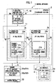
- the control apparatus 1 is configured for a self-diagnosis function, with: an operator 2 including a mutually diagnosing combination of first and second generalized processor cores 2a and 2b and a first dedicated processor core 4; a memory 5 for storing therein programs to be executed by the operator 2; an I/O interface 3 adapted for a processing for input and output signals to be controlled in the operator 2; and a normal bus 11 for normal connections and control within and among the operator 2, the memory 5, and the I/O interface 3.
- the first generalized processor core 2a, second generalized processor core 2b, and first dedicated processor core 4 are interconnected for JTAG tests by a boundary scan bus 12.
- the operator 2 is implemented with the first generalized processor core 2a, the second generalized processor core 2b, and the first dedicated processor core 4, which are formed as a combination on a common substrate, or as individual units on separate substrates.
- processor cores may be formed on separate semiconductor chips connected by inter-chip wirings, or on separate dies on a single semiconductor chip, the dies being connected by intra-chip wirings. In either case, the configuration in block diagram is identical to Fig. 1 .
- first generalized processor core 2a For each of first generalized processor core 2a, second generalized processor core 2b, and first dedicated processor core 4, its signal line TDI is serially connected a signal line TDO of another core, while unshown control lines are connected in parallel. Such signal lines and control lines constitute the boundary scan bus 12.
- processor cores are mounted in the embodiment, the number of processor cores to be implemented is not limited, providing that mounted two or more permit necessary connections by boundary scan bus.
- the first generalized processor core 2a, the second generalized processor core 2b, and the first dedicated processor core 4 have their I/O signal lines connected to the normal bus 11 of the control apparatus 1, which permits the operator 2 to give and receive control data to and from the memory 5 and the I/O interface 3, as necessary for execution of an associated control program.
- the first generalized processor core 2a includes: a first JTAG tester 22a connected to the boundary scan bus 12; a first intra-processor circuit 21a connected at one end thereof to the first JTAG tester 22a and at another end thereof to the normal bus 11, to be tested by the first JTAG tester 22a; and a control pattern setter 21c connected to the first intra-processor circuit 21a and configured to select a control program 53 or a first boundary scan control program 51a, whichever is to be executed by the operator 2, and have a control pattern of the control apparatus 1 preset to the first intra-processor circuit 21a.
- the control pattern is set as a selected one of three control modes: a "run” mode in which the control apparatus 1 runs simply under a normal control; an "intermittent test” mode in which the normal control is kept, while boundary scan tests are performed at preset periodical intervals without affecting the normal control; and a "test” mode in which simply boundary scan tests are performed.
- the first intra-processor circuit 21a performs a boundary scan test by a preset period, whereto a control pattern is preset by the control pattern setter 21c, and is read by the first intra-processor circuit 21a, and transmitted therefrom through the normal bus 11 to the second intra-processor circuit 21b, where it is set.
- the second generalizedprocessor core 2b includes: a second JTAG tester 22b connected to the boundary scan bus 12; and the above-noted second intra-processor circuit 21b, which is connected at one end thereof to the second JTAG tester 22b and at another end thereof to the normal bus 11, to be tested by the second JTAG tester 22b.
- the first dedicated processor core 4 includes: a fourth JTAG tester 42 connected to the boundary scan bus 12; and a fourth intra-processor circuit 41 connected at one end thereof to the fourth JTAG tester 42 and at another end thereof to the normal bus 11, to be tested by the fourth JTAG tester 42.
- the I/O interface 3 includes: a third JTAG tester 31 connected to the boundary scan bus 12; and an integrated circuit 32 connected to and tested by the third JTAG tester 31.
- the I/O interface 3 is connected to the normal bus 11, for transfer of input and output signals.
- the memory 5 has stored therein: a set of a first boundary scan control program 51a and a second boundary scan control program 51b for the operator 2 to perform boundary scan tests; a set of a first expected value data 52a and a second expected value data 52b each respectively to determine a conformity of a result of an associated boundary scan test; and the control program 53 for the operator 2 to perform a normal control.
- the first intra-processor circuit 21a samples the first boundary scan control program 51a and the first expected value data 52a, for use when boundary scan testing the second generalized processor core 2b.
- the second intra-processor circuit 21b samples the second boundary scan control program 51b and the second expected value data 52b, for use when boundary scan testing the first generalized processor core 2a.
- the first boundary scan control program 51a and the second boundary scan control program 51b, as well as the first expected value data 52a and the second expected value data 52b, should correspond to configurations of the first intra-processor circuit 21a and the second intra-processor circuit 21b, respectively. Accordingly, those will be different from each other, unless these are identical. However, if these are identical, those will also be identical, and will do with a set of control programs of a kind, and a set of value data of a kind.
- a control pattern preset by the control pattern setter 21c is read by the first intra-processor circuit 21a (step S1), and the first boundary scan control program 51a as a corresponding program is sampled from the memory 5 by the first intra-processor circuit 21a per se, where it is read in a register (step S2).
- the read first boundary scan control program 51a is followed, whereby the second processor core 2b is tested (step S3).
- a test signal is sent from the first intra-processor circuit 21a, through the boundary scan bus 12, to the second JTAG tester 22b, where it is sent to the second intra-processor circuit 21b, where a JTAG test is performed.
- the first intra-processor circuit 21a works to: send a test signal for testing the second processor core 2b, as an input signal through a signal line TDI of the boundary scan bus 12 to the second JTAG tester 22b; receive an output signal through a signal line TDO of the second JTAG tester 22b; and compare this with a preset first expected value data 52a for the second processor core 2b, to determine whether or not a trouble is present (step S4).
- an unshown preset trouble shooting program in the first boundary scan control program 51a is followed, to thereby execute a trouble shooting process including an interruption of control, notification, etc. (step S9).
- the first intra-processor circuit 21a sequentially performs: for the I/O interface 3, a test (step S5), and a determination of whether or not a trouble is present (step S6) ; and for the first dedicated processor core 4, a test (step S7), and a determination of whether or not a trouble is present (step S8).
- the first intra-processor circuit 21a Upon completion of whole tests on targets connected to the boundary scan bus 12, the first intra-processor circuit 21a gives, through the normal bus 11, a command to have the second intra-processor circuit 21a start a JTAG test.
- the second intra-processor circuit 21b works to: sample from the memory 5 the second boundary scan control program 51b and the second expected value data 52b; perform tests on targets connected to the boundary scan bus 12, i.e., the first generalized processor core 2a, the first dedicated processor core 4, and the I/O interface 3, in a prescribed order; determine whether or not a trouble is present for each of them; and execute a trouble shooting process if any trouble is present.
- control actions are similar to steps S1 to S9 in the flowchart of Fig. 4 .
- first intra-processor circuit 21a and the second intra-processor circuit 21b may do well with configurations for mutual tests on the second processor core 2b and the first processor core 2a, respectively. Other targets may be tested by either or both of them.
- decisions may depend on e.g. coincidence between input data and output data to judge states of connections up to I/O pins of intra-processor circuits and JTAG testers.
- Defaults in intra-processor circuits may be determined from functional tests of intra-processor circuits.
- the trouble shooting process may include a forced output of preset fail-safe data, or external trouble notification.
- a control apparatus 1 includes a pair of generalized processor cores each configured with a testing means to perform a boundary scan test and a target means to be boundary scan tested, thus allowing boundary scan tests to be mutually made.
- control apparatus 1 can be free of integrated circuits left unable to be self-diagnosed, allowing for an enhanced integrity in an entirety of the control apparatus 1.
- control apparatus is thus allowed to have an enhanced operation rate and an enhanced integrity together.
- control apparatus can be boundary scan tested inside, without interrupting control of its inherent processes, whereby troubles can be detected while running, thus allowing for an early detection of informality by self-diagnoses, even with severe restrictions to operation of control apparatus, such as response time.
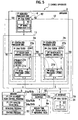
- the second embodiment is different from the first embodiment, as follows: In the latter, after mutual boundary scan tests on the generalized processor cores, their results are checked at the step S8 in the flowchart of Fig. 4 , and if any trouble is found there, the control flow goes to the step S9 to execute the trouble shooting process. Instead, in the former, design data and repairing data of intra-processor circuits are provided, and if any trouble is found in any intra-processor circuit at a step S8 in a flowchart of Fig. 6 , the control flow goes to a step S9 to execute a trouble shooting process, and additionally to a step S11 to execute a repairing process for repairing the intra-processor circuit.
- control apparatus 1 has implemented: a first design data writing controller 22al in a first JTAG tester 22a; and a second design data writing controller 22b1 in a second JTAG tester 22b.
- a design tool 6a configured to store therein first design data and first repairing data of a first intra-processor circuit 21a and a second intra-processor circuit 21b, and connected through a communication interface 61 therefor to a normal bus 11; and a combination of a repairing program 54a for the first intra-processor circuit 21a and a repairing program 54b for the second intra-processor circuit 21b, stored in a memory 5.
- the first intra-processor circuit 21a and the second intra-processor circuit 21b are typically provided with FPGAs or PLDs, and rewrite controllable.
- the first intra-processor circuit 21a works to: perform a boundary scan test on a second processor core 2b including the second intra-processor circuit 21b; identify troubling locations and circuits therein, if any, from results of the test; and as shown by broken line arrows in Fig. 5 , sample repairing data relating to such troubles from the design tool 6a, and send them through a boundary scan bus 12, whereby the second design data writing controller 22b1 is driven to rewrite corresponding design data of the second intra-processor circuit 21b stored in an associated nonvolatile memory (FROM).
- FROM nonvolatile memory
- the second intra-processor circuit 21b identifies troubling locations and circuits, if any, in a first processor core 2a including the first intra-processor circuit 21a, and drives the first design data writing controller 22al to rewrite corresponding design data of the first intra-processor circuit 21a stored in an associated nonvolatile memory (FROM).
- FROM nonvolatile memory
- control apparatus 1 is connected with the design tool 6a by communications to acquire repairing data, and reconfigurable (rewritable) processor cores' JTAG testers are provided with writing controllers adapted for design data of troubling locations of intra-processor circuits to be rewritten by the repairing data.
- the intra-processor circuits are automatically changeable. Further, using such devices as reconfigurable while working, the intra-processor circuits can be repaired even when the control apparatus is running.
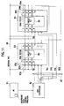
- the third embodiment is different from the second embodiment, as follows: In the latter, a mutual boundary scan test is performed between a pair of generalized processor cores each configured for the contents of operation to be programmable by software. Instead, in the former, a mutual boundary scan test is performed between a first generalized processor core 2a, and a second dedicated processor core 7 configured with hardware for a fixed content of operation.
- the second dedicated processor core 7 is configured with: a fifth intra-processor circuit 71; a fifth JTAG tester 72 provided with a third design data writing controller 72b; and a JTAG controller 73 for commanding, through a boundary scan bus 12, a boundary scan control for a test on the first generalized processor core 2a.
- a third boundary scan control program 51c for a test on the second dedicated processor core 7 a third expected value data 52c as a reference data for determination of a trouble on a result of the test by the third boundary scan control program 51c; a fourth expected value data 52d as a reference data for determination of presence or absence of a trouble on a result of the test by the JTAG controller 73; a repairing program 54c for repairing the first generalized processor core 2a; and a repairing program 54d for repairing the second dedicated processor core 7.
- a design tool 6b has stored therein sets of second design data and second repairing data of a first intra-processor circuit 21a and the fifth intra-processor circuit 71.
- the fifth intra-processor circuit 71 commands the JTAG controller 73 to start the test.
- the JTAG controller 73 works to: perform the test on the first processor core 2a through the boundary scan bus 12; and compare a result of the test with the fourth expected value data 52d; and for any trouble identified, to drive the repairing program 54d, to sample a second repairing data, and control a third design data writing controller 22al to write the repairing data in a nonvolatile memory (FROM) of the first intra-processor circuit 21a.
- FROM nonvolatile memory
- the first intra-processor circuit 21a performs a boundary scan test on the second dedicated processor core 7, whereof associated actions are identical to the first embodiment providing that the former substitutes the second dedicated processor core 7 for the second generalized processor core 2b in the latter, and redundant description is omitted.
- a generalized processor core and a dedicated processor core are each configured with a testing means to perform a boundary scan test and a target means to be boundary scan tested, thus allowing boundary scan tests to be mutually made even in the pair of processor cores including a dedicated one.
- a control apparatus 1 according to a fourth embodiment of the present invention, with reference to Fig. 8 to Fig. 10 .
- the former is different in that a memory 5 has stored therein a number of rows of test data as a set of test history data 54e, and like elements are designated by like reference characters in Fig. 8 , to eliminate redundant description.
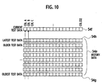
- the third embodiment includes a configuration for a check for a transient error occurring in an intermittent test mode, to continue this mode upon an occurrence of transient error. More specifically, as shown in a flowchart of Fig. 9 , after a sequence of steps S1 to S10 corresponding to those for an intermittent test in the flowchart of the first embodiment shown in Fig. 4 , the third embodiment has an additional step S12 for a current string of test data 54f to be stored in a region of test history data 54e in the memory 5, as illustrated in Fig. 10 , where strings of test data in the past are stored as an array of rows to be checked by columns A, B, C, ..., ZZZ that one-to-one correspond to testing locations in the processor cores 2a and 2b as test targets.
- the storage region of test history data 54e has a limited maximal size, so a row of oldest test data 54g is shifted out when the current string of test data 54f is added as a new row.
- Each column in the new row of test data 54f is compared with a correspondent existing test data 54e, e. g. a correspondent data in a row of latest test data 54h, to make a check for an inconsistency in between to be recorded as an error at the column.
- a correspondent existing test data 54e e. g. a correspondent data in a row of latest test data 54h
- each time when a new row of test data 54 f is added such column-wise checks are repeated. And, if any column having a recorded error is restored to be consistent in a check within a prescribed period of time after a first recording of the error, this event is identified as an occurrence of transient error (YES at step S13), which is logged as part of an entire set of test history data 54e, together with a label of a testing location where the transient error has occurred (step S14).
- boundary scan tests are made on processors, but may well be implemented for inspection of memories, such as a flush memory, using a boundary scan bus.
Landscapes
- Engineering & Computer Science (AREA)
- General Engineering & Computer Science (AREA)
- Physics & Mathematics (AREA)
- General Physics & Mathematics (AREA)
- Theoretical Computer Science (AREA)
- Computer Hardware Design (AREA)
- Quality & Reliability (AREA)
- Tests Of Electronic Circuits (AREA)
- Test And Diagnosis Of Digital Computers (AREA)
Abstract
Description
- The present invention relates to a control apparatus for controlling a process, such as in a steel-making plant or a petrochemical plant, and particularly, to a control apparatus including an operator provided with processor cores, and subjected to boundary scan tests.
- A boundary scan test (sometimes referred herein simply to "JTAG test") proposed by the JTAG (Joint Test Action Group) was standardized as the IEEE Standard 1149.1-1990, as a method of testing eletronics implemented with integrated circuits difficult of a probing board inspection.
- The JTAG test will be described with reference to
Fig. 11 . For the JTAG test, for example, control apparatuses are configured with: a pair ofJTAG testers target circuits dedicated lines 87 for a daisy chain connection of theJTAG testers JTAG controller 82 for driving theJTAG testers JTAG controller 82. - Typically, the set of
dedicated lines 87 includes a pair of signal lines being a TDI (i.e. a signal line connected to a 'Test Data Input' terminal) and a TDO (i.e. a signal line connected to a 'Test Data Output' terminal) to be connected in series, and a triple of control lines being a TMS (i.e. a signal line connected to a 'Test Mode Select' terminal), a TCK (i.e. a signal line connected to a 'Test ClocK' terminal), and a TRST (i.e. a signal line connected to a 'Test ReSeT' terminal) to be connected in parallel. Such a set of lines is provided as a boundary scan bus. - As illustrated in
Fig. 11 , signal lines TDI for data to be input and signal lines TDO for data to be output are chained for a serial connection through theJTAG tester 83,target circuit 85,JTAG tester 84, andtarget circuit 86, starting from and ending on theJTAG controller 82. The control lines are connected in parrallel to the target circuits, and serve to control the transfer of input data and output data through the signal lines TDI and TDO. - The
JTAG tester 83 has: a set of I/O (input/output)terminals 83a corresponding to I/O pins 83c of thetarget circuit 85 to be mounted; and a set ofboundary scan cells 83b for scanning input data and output data between the set of I/O terminals 83a and thetarget circuit 85. TheJTAG tester 83 is configured to shift a sequence of bits serially output from theJTAG controller 82 as data to be input through a signal line TDI, and whole output data from associatedboundary scan cells 83b as data to be output through a signal line TDO. - Likewise, the
JTAG tester 84 has: a set of I/O terminals 84a corresponding to I/O pins 84c of thetarget circuit 86 to be mounted; and a set of boundary scan cells 84b for scanning input data and output data between the set of I/O terminals 84a and thetarget circuit 86. TheJTAG tester 84 is configured to shift a sequence of bits serially output from theJTAG controller 82 as data to be input through a signal line TDI, and whole output data from associated boundary scan cells 84b as data to be output through a signal line TDO. - The
JTAG controller 82 follows the boundary scan control program, as it is preset, to transmit serial data to be input through a signal line TDI, receive output data from thetarget circuits - The I/
O terminals 83a and 84a are connected to anormal bus 88 for transmission of input signals and output signals to be processed therethrough in a normal control mode where thetarget circuits - For an improved integrity of electronics provided with such JTAG testers, there have been proposed techniques in which an electronic apparatus per se is configured to function each time when powered on, for an automatic boundary scan to diagnose itself for anormality (refer to patent document 1).
- Patent document 1: Japanese Patent Application Laying-Open Publication No.
9-5400 - Conventional boundary scan testing devices have been unable to quickly cope with accidental troubles thereon, and some have employed a boundary scan controlling device to have simple boundary scan commands executed for, among others, a startup of a self-testing function to boundary scan compliance ICs on a printed circuit board, or a read-in from specific registers in such IC's (refer to patent document 2).
- Patent document 2: Japanese Patent Application Laying-Open Publication No.
2000-206202 - On the other hand, in the field of a control apparatus for controlling processes, such as in a steel-making or petrochemical plant, recent years have observed a number of presentations on a control apparatus including a plurality of processor cores (sometimes called a multi-core).
- Processor cores constituting the multi-core encompass, among others, a generalized processor core for processing a general-purpose command capable of a programming by software, for example, and a dedicated processor core for processing a specific operation such as for an audio or video, for example.
- The former is suitable for implementation of a generic processing, and the latter affords to implemnt a specific processing with high speed and low power dissipation. This accounts for an increased proportion of a multi-core control apparatus configured with a plurality of processors simply generalized or dedicated, or as a hybrid of generalized or dedicated processors.
- The control apparatus is accompanied by an advancing application of reconfigurable devices, e.g. an FGPA (Field Program Gate Array), a PLD (Programmable Logic Device), etc, as harwares for processor cores to be implemented thereon. The FGPA, PLD, and the like allow for a voluntary reconfiguration of circuitry even after implementation on a substrate, as an advantage.
- For occasional increases in number of protocols to be executed or revisions of standards to be complied with, circuit-reconfigurable FGPAs and PLDs have been employed for processor cores dedicated for specific processings, control cores for transmission, and so on.
- Control apparatueses provided with such FPGAs or PLDs are subjected to, among others, a trouble shooting of control apparatus, and a renewal of circuitry composed of such devices in control appartus, whereto an efficient technique using a network has been proposed (refer to patent document 3).
- Patent document 3: Japanese Patent Application Laying-Open Publication No.
2001-306343 - The
patent document 3 has disclosed an apparatus with FPGAs, which has a CPU, a memory, a set of networking elements, and the FPGAs, and is adapted to reconfigure the FPGAs' design data, from a terminal allowed to have an access to the apparatus with FPGAs through a managing apparatus linked by a network. - With a recent trend for a control apparatus to be provided with a plurality of processor cores, there is a tendency for the control apparatus to have an enlarged circuit scale, with an increase in number of I/O pins of integrated circuits constituting processor cores or the like.
- Concurrently with the increase in pin number of integrated circuits, micro-fabrication of wiring is advancing in such integrated circuits, as well as on substrates for integrated circuits to be mounted thereon, whereby it is becoming important for a secured integrity of control apparatus to provide functions of, among others, finding defaults due to break or contact failure upon implementation of integrated circuits on substrates, and defective locations in circuitry of the integrated circuits per se, and reconfiguring integrated circuits in trouble.
- For such troubles that might be occasional, inspections by in-circuit testers could not afford to quickly cope with, and the control apparatus should be adapted to perform boundary scan tests even in its working state.
- For the electronic described in the
patent document 1, it is possible to perform boundary scan tests to integrated circuits realizing principal functions of the electronic, to thereby inspect them for anormality. However, there is no provision of a mechanism for inspecting such testing devices per se that are provided to perform the boundary scan tests. - There is thus no way to perform a self-diagnosis for anormality in the boundary scan testing devices, and it is impossible to discriminate whether troubling is a boundary scan testing device or an integrated circuit as a test target, as a problem.
- The testing devices are put in a similar environment to integrated circuits, and are subjected to troubles like the integrated circuits. The provision of testing devices thus constitutes an addition of non-testable devices impeding enhancement of integrity of the apparatus, as an issue.
- For the printed circuit board described in the
patent document 2 also, there is a problem to occur like thepatent document 1. That is, although thepatent document 2 includes a boundary scan controller of a simplified type adapted to diagnose boundary scan compliance ICs, it is impossible for the printed circuit board to solely diagnose the simplified boundary scan controller itself, as a problem. - For the apparatus with FPGAs described in the
patent document 3, it is permitted to receive the FPGAs' design data given via the managing apparatus linked by the network, allowing for a renewal of internal circuits of FPGAs of the apparatus. - However, for the renewal of FPGA circuits, the apparatus with FPGAs should have a renewal processor to implement a renewal processing therein, but is disabled to handle the renewal processor per se as a renewal target, with a necessity for a renewal of design data of the renewal processor itself to provide this renewal processor with another renewal processor, as a problem.
- The present invention has been devised in view of such points. It therefore is an object of the present invention to provide a control apparatus adapted for self-diagnoses of processor cores of an operator of the control apparatus and devices for their self-diagnoses, allowing for boundary scan tests even when running, and self-repairing of defective locations of processor cores of the operator.
- According to an aspect of the present invention, a control apparatus comprises an operator including a pair of processor cores connected to a boundary scan bus, and adapted to mutually diagnose opponent processor cores in between, a memory configured to store therein data and programs to be executed by the operator, an I/O interface configured for input and output signals to be processed for associated processes in the operator, and a normal bus configured for normal connections among the operator, the memory, and the I/O interface, the operator comprises a first generalized processor core and a second generalized processor core each respectively connected to the boundary scan bus, the memory has a set of a first boundary scan control program and a second boundary scan control program for the operator to perform boundary scan tests, a first expected value data and a second expected value data each respectively to determine a conformity of a result of an associated boundary scan test, and a control program for the operator to perform a control, the first generalized processor core comprises a first boundary scan tester, a first intra-processor circuit to be tested by the first boundary scan tester, and a control pattern setter configured for selection of the control program or the set of the first and second boundary scan control programs, whichever is to be executed by the operator, to have a control pattern of the control apparatus preset to the first intra-processor circuit, the second generalized processor core comprises a second boundary scan tester, and a second intra-processor circuit to be tested by the second boundary scan tester, and the control pattern is followed for a time-dividing implementation of and between a boundary scan test to be performed to the second generalized processor core, through the boundary scan bus, by and from the first intra-processor circuit having the first boundary scan control program sampled there-for, and a boundary scan test to be performed to the first generalized processor core, through the boundary scan bus, by and from the second intra-processor circuit having the second boundary scan control program sampled there-for, depending on a diagnosis request command received from the first intra-processor circuit, through the normal bus, in accordance with a setting of the control pattern.
- According to another aspect of the present invention, a control apparatus comprises an operator including a pair of processor cores connected to a boundary scan bus, and adapted to mutually diagnose opponent processor cores in between, a memory configured to store therein data and programs to be executed by the operator, an I/O interface configured for input and output signals to be processed for associated processes in the operator, and a normal bus configured for normal connections among the operator, the memory, and the I/O interface, the operator comprises a first generalized processor core and a second dedicated processor core each respectively connected to the boundary scan bus, the memory has a set of a third boundary scan control program and a fourth boundary scan control program for the operator to perform boundary scan tests, a third expected value data and a fourth expected value data each respectively to determine a conformity of a result of an associated boundary scan test, and a control program for the operator to perform a control, the first generalized processor core comprises a first boundary scan tester, a first intra-processor circuit to be tested by the first boundary scan tester, and a control pattern setter configured for selection of the control program or the third boundary scan control program, whichever is to be executed by the operator, to have a control pattern of the control apparatus preset to the first intra-processor circuit, the second dedicated processor core comprises a fifth boundary scan tester, a fifth intra-processor circuit to be tested by the fifth boundary scan tester, and a boundary scan controller configured to test the first generalized processor core connected to the boundary scan bus, and the control pattern is followed for a time-dividing implementation of and between a boundary scan test to be performed to the second dedicated processor core, through the boundary scan bus, by and from the first intra-processor circuit having the third boundary scan control program sampled therefor, and a boundary scan test to be performed to the first generalized processor core, through the boundary scan bus, by and from the boundary scan controller driven by the fifth intra-processor circuit with a diagnosis request command received in accordance with the control pattern, from the first intra-processor circuit, through the normal bus.
- According to another aspect of the present invention, a control apparatus comprises an operator comprising a plurality of processor cores connected to a boundary scan bus, and boundary scan tested from each other for a mutual diagnosis in between in a time-dividing manner.
- According to any one of the aspects, a control apparatus is adapted for self-diagnoses of processor cores of an operator of the control apparatus and devices for their self-diagnoses, allowing for boundary scan tests even when running, and self-repairing of defective locations of processor cores of the operator.
-
-
Fig. 1 is a block diagram of a control apparatus according to a first embodiment of the present invention. -
Fig. 2 is a block diagram illustrating a testing configuration in accordance with the present invention. -
Fig. 3 is a table listing exemplary modes of a control pattern in accordance with the present invention. -
Fig. 4 is a flowchart of control actions for JTAG tests according to the first embodiment of the present invention. -
Fig. 5 is a block diagram of a control apparatus according to a second embodiment of the present invention. -
Fig. 6 is a flowchart of control actions for JTAG tests according to the second embodiment of the present invention. -
Fig. 7 is a block diagram of a control apparatus according to a third embodiment of the present invention. -
Fig. 8 is a block diagram of a control apparatus according to a fourth embodiment of the present invention. -
Fig. 9 is a flowchart of control actions for JTAG tests according to the fourth embodiment of the present invention. -
Fig. 10 is a diagram of a structure of a set of test history data in the control apparatus according to the fourth embodiment of the present invention. -
Fig. 11 is a block diagram of a conventional boundary scan tester. - There will be described embodiments of the present invention, with reference to the drawings.
- There will be described below a first embodiment of the present invention, with reference to
Fig. 1 to Fig. 4 . Description is now made with reference toFig. 2 , which illustrates a configuration of a JTAG testing device for a self-diagnosing test in accordance with the present invention. Relative to the JTAG testing device inFig. 11 , like elements are designated by like reference characters inFig. 2 , to eliminate redundant description. - The JTAG testing device illustrated in
Fig. 2 is different from the JTAG testing device inFig. 11 . In the latter, boundary scans on thetarget circuits JTAG controller 82 following a boundary scan control program provided in thePC 81. Instead, in the former, anintra-processor circuit 85a mounted on atarget circuit 85 is configured to test aprocessor core 200 composed of aJTAG tester 84 and anothertarget circuit 86, and anotherintra-processor circuit 86a mounted on thistarget circuit 86 is configured to test aprocessor core 100 composed of anotherJTAG tester 83 and thattarget circuit 85a. - In other words, paired
processor cores intra-processor circuit 85a at one side diagnoses aprocessor core 200 at the other side, and theintra-processor circuit 86a at this side diagnoses aprocessor core 200 at that side. - The
processor core 100 and theprocessor core 200 are mutually connected for their boundary scan tests by a boundary scan bus composed of a dedicated line set 87 of five lines as a combination of serially connected signal lines TDI and TDO and parallel-connected control lines TMS, TCK, and TRST, whereby theintra-processor circuit 85a at one side is adapted to drive theboundary scan tester 84 at the other side, so that thisboundary scan tester 84 and itsintra-processor circuit 86a, both mounted typically on a substrate, are tested at once. - Likewise, the
intra-processor circuit 86a at this side is adapted to drive theJTAG tester 83 at that side, so that thisJTAG tester 84 and itsintra-processor circuit 85a, both mounted typically on a substrate, are tested at once. Thus, both processor cores are adapted to mutually diagnose entireties of opponent processor cores in a time-dividing manner. - Both
intra-processor circuits O terminals 83a and 84a connected to anormal bus 88, so they can make their normal control actions through thebus 88, while boundary scan tests are performed through the boundary scan bus. In this configuration, the control and the testing are performed in a time-dividing manner. - Description is now made of a
control apparatus 1 according to the first embodiment, with reference toFig. 1 , where the foregoing concept of JTAG testing device prevails. Thecontrol apparatus 1 is configured for a self-diagnosis function, with: anoperator 2 including a mutually diagnosing combination of first and secondgeneralized processor cores dedicated processor core 4; amemory 5 for storing therein programs to be executed by theoperator 2; an I/O interface 3 adapted for a processing for input and output signals to be controlled in theoperator 2; and anormal bus 11 for normal connections and control within and among theoperator 2, thememory 5, and the I/O interface 3. - The first
generalized processor core 2a, secondgeneralized processor core 2b, and firstdedicated processor core 4 are interconnected for JTAG tests by aboundary scan bus 12. - Description is now made of component configurations. The
operator 2 is implemented with the firstgeneralized processor core 2a, the secondgeneralized processor core 2b, and the firstdedicated processor core 4, which are formed as a combination on a common substrate, or as individual units on separate substrates. - Those processor cores may be formed on separate semiconductor chips connected by inter-chip wirings, or on separate dies on a single semiconductor chip, the dies being connected by intra-chip wirings. In either case, the configuration in block diagram is identical to
Fig. 1 . - For each of first
generalized processor core 2a, secondgeneralized processor core 2b, and firstdedicated processor core 4, its signal line TDI is serially connected a signal line TDO of another core, while unshown control lines are connected in parallel. Such signal lines and control lines constitute theboundary scan bus 12. - Although three processor cores are mounted in the embodiment, the number of processor cores to be implemented is not limited, providing that mounted two or more permit necessary connections by boundary scan bus.
- The first
generalized processor core 2a, the secondgeneralized processor core 2b, and the firstdedicated processor core 4 have their I/O signal lines connected to thenormal bus 11 of thecontrol apparatus 1, which permits theoperator 2 to give and receive control data to and from thememory 5 and the I/O interface 3, as necessary for execution of an associated control program. - The first
generalized processor core 2a includes: afirst JTAG tester 22a connected to theboundary scan bus 12; a firstintra-processor circuit 21a connected at one end thereof to thefirst JTAG tester 22a and at another end thereof to thenormal bus 11, to be tested by thefirst JTAG tester 22a; and acontrol pattern setter 21c connected to the firstintra-processor circuit 21a and configured to select acontrol program 53 or a first boundaryscan control program 51a, whichever is to be executed by theoperator 2, and have a control pattern of thecontrol apparatus 1 preset to the firstintra-processor circuit 21a. - Description is now made of the control pattern to be set by the
control pattern setter 21c, with reference toFig. 3 . The control pattern is set as a selected one of three control modes: a "run" mode in which thecontrol apparatus 1 runs simply under a normal control; an "intermittent test" mode in which the normal control is kept, while boundary scan tests are performed at preset periodical intervals without affecting the normal control; and a "test" mode in which simply boundary scan tests are performed. - The first
intra-processor circuit 21a, as well as a later-described secondintra-processor circuit 21b, performs a boundary scan test by a preset period, whereto a control pattern is preset by thecontrol pattern setter 21c, and is read by the firstintra-processor circuit 21a, and transmitted therefrom through thenormal bus 11 to the secondintra-processor circuit 21b, where it is set. - The
second generalizedprocessor core 2b includes: asecond JTAG tester 22b connected to theboundary scan bus 12; and the above-noted secondintra-processor circuit 21b, which is connected at one end thereof to thesecond JTAG tester 22b and at another end thereof to thenormal bus 11, to be tested by thesecond JTAG tester 22b. - The first
dedicated processor core 4 includes: afourth JTAG tester 42 connected to theboundary scan bus 12; and a fourthintra-processor circuit 41 connected at one end thereof to thefourth JTAG tester 42 and at another end thereof to thenormal bus 11, to be tested by thefourth JTAG tester 42. - The I/
O interface 3 includes: athird JTAG tester 31 connected to theboundary scan bus 12; and anintegrated circuit 32 connected to and tested by thethird JTAG tester 31. The I/O interface 3 is connected to thenormal bus 11, for transfer of input and output signals. - The
memory 5 has stored therein: a set of a first boundaryscan control program 51a and a second boundaryscan control program 51b for theoperator 2 to perform boundary scan tests; a set of a first expectedvalue data 52a and a second expectedvalue data 52b each respectively to determine a conformity of a result of an associated boundary scan test; and thecontrol program 53 for theoperator 2 to perform a normal control. - The first
intra-processor circuit 21a samples the first boundaryscan control program 51a and the first expectedvalue data 52a, for use when boundary scan testing the secondgeneralized processor core 2b. The secondintra-processor circuit 21b samples the second boundaryscan control program 51b and the second expectedvalue data 52b, for use when boundary scan testing the firstgeneralized processor core 2a. - The first boundary
scan control program 51a and the second boundaryscan control program 51b, as well as the first expectedvalue data 52a and the second expectedvalue data 52b, should correspond to configurations of the firstintra-processor circuit 21a and the secondintra-processor circuit 21b, respectively. Accordingly, those will be different from each other, unless these are identical. However, if these are identical, those will also be identical, and will do with a set of control programs of a kind, and a set of value data of a kind. - Description is now made of actions of the
control apparatus 1, with reference to the flowchart ofFig. 4 . First, a control pattern preset by thecontrol pattern setter 21c, to be "intermittent test" or "test" mode, is read by the firstintra-processor circuit 21a (step S1), and the first boundaryscan control program 51a as a corresponding program is sampled from thememory 5 by the firstintra-processor circuit 21a per se, where it is read in a register (step S2). - The read first boundary
scan control program 51a is followed, whereby thesecond processor core 2b is tested (step S3). - That is, in accordance with the first boundary
scan control program 51a, a test signal is sent from the firstintra-processor circuit 21a, through theboundary scan bus 12, to thesecond JTAG tester 22b, where it is sent to the secondintra-processor circuit 21b, where a JTAG test is performed. - More specifically, the first
intra-processor circuit 21a works to: send a test signal for testing thesecond processor core 2b, as an input signal through a signal line TDI of theboundary scan bus 12 to thesecond JTAG tester 22b; receive an output signal through a signal line TDO of thesecond JTAG tester 22b; and compare this with a preset first expectedvalue data 52a for thesecond processor core 2b, to determine whether or not a trouble is present (step S4). - For a determination for presence of a trouble, an unshown preset trouble shooting program in the first boundary
scan control program 51a is followed, to thereby execute a trouble shooting process including an interruption of control, notification, etc. (step S9). - Likewise, the first
intra-processor circuit 21a sequentially performs: for the I/O interface 3, a test (step S5), and a determination of whether or not a trouble is present (step S6) ; and for the firstdedicated processor core 4, a test (step S7), and a determination of whether or not a trouble is present (step S8). - Upon completion of whole tests on targets connected to the
boundary scan bus 12, the firstintra-processor circuit 21a gives, through thenormal bus 11, a command to have the secondintra-processor circuit 21a start a JTAG test. - Then, the second
intra-processor circuit 21b works to: sample from thememory 5 the second boundaryscan control program 51b and the second expectedvalue data 52b; perform tests on targets connected to theboundary scan bus 12, i.e., the firstgeneralized processor core 2a, the firstdedicated processor core 4, and the I/O interface 3, in a prescribed order; determine whether or not a trouble is present for each of them; and execute a trouble shooting process if any trouble is present. - For the second
intra-processor circuit 21b, control actions are similar to steps S1 to S9 in the flowchart ofFig. 4 . - It is noted that the first
intra-processor circuit 21a and the secondintra-processor circuit 21b may do well with configurations for mutual tests on thesecond processor core 2b and thefirst processor core 2a, respectively. Other targets may be tested by either or both of them. - For presence or absence of a trouble to be determined by JTAG tests (step S8), decisions may depend on e.g. coincidence between input data and output data to judge states of connections up to I/O pins of intra-processor circuits and JTAG testers.
- Defaults in intra-processor circuits may be determined from functional tests of intra-processor circuits.
- For troubles identified by such determination, if they are e.g. circuit troubles, the trouble shooting process (step S9) may include a forced output of preset fail-safe data, or external trouble notification.
- According to the embodiment described, a
control apparatus 1 includes a pair of generalized processor cores each configured with a testing means to perform a boundary scan test and a target means to be boundary scan tested, thus allowing boundary scan tests to be mutually made. - Configurations in the past had no means for testing a testing device per se needed to perform a boundary scan test, and were unable to self-diagnose the testing device for a trouble. However, according to the present embodiment in which processor cores can be mutually boundary scan tested, the
control apparatus 1 can be free of integrated circuits left unable to be self-diagnosed, allowing for an enhanced integrity in an entirety of thecontrol apparatus 1. - Moreover, troubles canbe found in a self-diagnosingmanner, without provision of additional testing devices, and hence without increased component numbers. The control apparatus is thus allowed to have an enhanced operation rate and an enhanced integrity together.
- Further, the control apparatus can be boundary scan tested inside, without interrupting control of its inherent processes, whereby troubles can be detected while running, thus allowing for an early detection of informality by self-diagnoses, even with severe restrictions to operation of control apparatus, such as response time.
- Description is now made of a
control apparatus 1 according to a second embodiment of the present invention, with reference toFig. 5 andFig. 6 . Relative to thecontrol apparatus 1 in the first embodiment, like elements are designated by like reference characters inFig. 5 , to eliminate redundant description. - The second embodiment is different from the first embodiment, as follows: In the latter, after mutual boundary scan tests on the generalized processor cores, their results are checked at the step S8 in the flowchart of
Fig. 4 , and if any trouble is found there, the control flow goes to the step S9 to execute the trouble shooting process. Instead, in the former, design data and repairing data of intra-processor circuits are provided, and if any trouble is found in any intra-processor circuit at a step S8 in a flowchart ofFig. 6 , the control flow goes to a step S9 to execute a trouble shooting process, and additionally to a step S11 to execute a repairing process for repairing the intra-processor circuit. - According to the second embodiment, the
control apparatus 1 has implemented: a first design data writing controller 22al in afirst JTAG tester 22a; and a second design data writing controller 22b1 in asecond JTAG tester 22b. - Further, it has: a
design tool 6a configured to store therein first design data and first repairing data of a firstintra-processor circuit 21a and a secondintra-processor circuit 21b, and connected through acommunication interface 61 therefor to anormal bus 11; and a combination of a repairingprogram 54a for the firstintra-processor circuit 21a and a repairingprogram 54b for the secondintra-processor circuit 21b, stored in amemory 5. - The first
intra-processor circuit 21a and the secondintra-processor circuit 21b are typically provided with FPGAs or PLDs, and rewrite controllable. - The first
intra-processor circuit 21a works to: perform a boundary scan test on asecond processor core 2b including the secondintra-processor circuit 21b; identify troubling locations and circuits therein, if any, from results of the test; and as shown by broken line arrows inFig. 5 , sample repairing data relating to such troubles from thedesign tool 6a, and send them through aboundary scan bus 12, whereby the second design data writing controller 22b1 is driven to rewrite corresponding design data of the secondintra-processor circuit 21b stored in an associated nonvolatile memory (FROM). - Likewise, the second
intra-processor circuit 21b identifies troubling locations and circuits, if any, in afirst processor core 2a including the firstintra-processor circuit 21a, and drives the first design data writing controller 22al to rewrite corresponding design data of the firstintra-processor circuit 21a stored in an associated nonvolatile memory (FROM). - In the second embodiment described, the
control apparatus 1 is connected with thedesign tool 6a by communications to acquire repairing data, and reconfigurable (rewritable) processor cores' JTAG testers are provided with writing controllers adapted for design data of troubling locations of intra-processor circuits to be rewritten by the repairing data. - Therefore, the intra-processor circuits are automatically changeable. Further, using such devices as reconfigurable while working, the intra-processor circuits can be repaired even when the control apparatus is running.
- Description is now made of a
control apparatus 1 according to a third embodiment of the present invention, with reference toFig. 7 . Relative to thecontrol apparatus 1 in the second embodiment, like elements are designated by like reference characters inFig. 7 , to eliminate redundant description. - The third embodiment is different from the second embodiment, as follows: In the latter, a mutual boundary scan test is performed between a pair of generalized processor cores each configured for the contents of operation to be programmable by software. Instead, in the former, a mutual boundary scan test is performed between a first
generalized processor core 2a, and a seconddedicated processor core 7 configured with hardware for a fixed content of operation. - In the third embodiment, the second
dedicated processor core 7 is configured with: a fifthintra-processor circuit 71; afifth JTAG tester 72 provided with a third designdata writing controller 72b; and aJTAG controller 73 for commanding, through aboundary scan bus 12, a boundary scan control for a test on the firstgeneralized processor core 2a. - It has in a memory 5: a third boundary
scan control program 51c for a test on the seconddedicated processor core 7; a third expectedvalue data 52c as a reference data for determination of a trouble on a result of the test by the third boundaryscan control program 51c; a fourth expectedvalue data 52d as a reference data for determination of presence or absence of a trouble on a result of the test by theJTAG controller 73; a repairingprogram 54c for repairing the firstgeneralized processor core 2a; and a repairingprogram 54d for repairing the seconddedicated processor core 7. - Further, a
design tool 6b has stored therein sets of second design data and second repairing data of a firstintra-processor circuit 21a and the fifthintra-processor circuit 71. - For the
control apparatus 1 configured as described in accordance with the third embodiment, description is now made of the seconddedicated processor core 7 given a command for a test from the firstintra-processor circuit 21a through anormal bus 11. - Given the command for a test from the first
intra-processor circuit 21a through thenormal bus 11, the fifthintra-processor circuit 71 commands theJTAG controller 73 to start the test. - Then, the
JTAG controller 73 works to: perform the test on thefirst processor core 2a through theboundary scan bus 12; and compare a result of the test with the fourth expectedvalue data 52d; and for any trouble identified, to drive the repairingprogram 54d, to sample a second repairing data, and control a third design data writing controller 22al to write the repairing data in a nonvolatile memory (FROM) of the firstintra-processor circuit 21a. - In the third embodiment, the first
intra-processor circuit 21a performs a boundary scan test on the seconddedicated processor core 7, whereof associated actions are identical to the first embodiment providing that the former substitutes the seconddedicated processor core 7 for the secondgeneralized processor core 2b in the latter, and redundant description is omitted. - According to the third embodiment described, a generalized processor core and a dedicated processor core, paired for use, are each configured with a testing means to perform a boundary scan test and a target means to be boundary scan tested, thus allowing boundary scan tests to be mutually made even in the pair of processor cores including a dedicated one.
- Description is now made of a
control apparatus 1 according to a fourth embodiment of the present invention, with reference toFig. 8 to Fig. 10 . Relative to thecontrol apparatus 1 of the first embodiment shown inFig. 1 , the former is different in that amemory 5 has stored therein a number of rows of test data as a set oftest history data 54e, and like elements are designated by like reference characters inFig. 8 , to eliminate redundant description. - The third embodiment includes a configuration for a check for a transient error occurring in an intermittent test mode, to continue this mode upon an occurrence of transient error. More specifically, as shown in a flowchart of
Fig. 9 , after a sequence of steps S1 to S10 corresponding to those for an intermittent test in the flowchart of the first embodiment shown inFig. 4 , the third embodiment has an additional step S12 for a current string oftest data 54f to be stored in a region oftest history data 54e in thememory 5, as illustrated inFig. 10 , where strings of test data in the past are stored as an array of rows to be checked by columns A, B, C, ..., ZZZ that one-to-one correspond to testing locations in theprocessor cores test history data 54e has a limited maximal size, so a row ofoldest test data 54g is shifted out when the current string oftest data 54f is added as a new row. - Each column in the new row of
test data 54f is compared with a correspondent existingtest data 54e, e. g. a correspondent data in a row oflatest test data 54h, to make a check for an inconsistency in between to be recorded as an error at the column. Each time when a new row oftest data 54 f is added, such column-wise checks are repeated. And, if any column having a recorded error is restored to be consistent in a check within a prescribed period of time after a first recording of the error, this event is identified as an occurrence of transient error (YES at step S13), which is logged as part of an entire set oftest history data 54e, together with a label of a testing location where the transient error has occurred (step S14). So long as any and all associated inconsistency is verified to be transient or in a course of verification within the prescribed period of time, as well as when no inconsistency is recorded, the intermittent test mode is kept frombeing interrupted, and hence is continued. It is noted that each time when a new row oftest data 54f is added, its data may be column-wise sequentially compared with whole existingdata 54e, from an oldest one 54g up to a latest one 54h, for verification of a transient error. - It also is noted that the foregoing boundary scan tests are made on processors, but may well be implemented for inspection of memories, such as a flush memory, using a boundary scan bus.
- While preferred embodiments of the present invention have been described using specific terms, such description is for illustrative purposes, and it is to be understood that changes and variations may be made without departing from the scope of the following claims.
Claims (9)
- A control apparatus comprising:an operator including a pair of processor cores connected to a boundary scan bus, and adapted to mutually diagnose opponent processor cores in between;a memory configured to store therein data and programs to be executed by the operator;an I/O interface configured for input and output signals to be processed for associated processes in the operator; anda normal bus configured for normal connections among the operator, the memory, and the I/O interface, whereinthe operator comprises a first generalized processor core and a second generalized processor core each respectively connected to the boundary scan bus,the memory has a set of a first boundary scan control program and a second boundary scan control program for the operator to perform boundary scan tests, a first expected value data and a second expected value data each respectively to determine a conformity of a result of an associated boundary scan test, and a control program for the operator to perform a control,the first generalized processor core comprises a first boundary scan tester, a first intra-processor circuit to be tested by the first boundary scan tester, and a control pattern setter configured for selection of the control program or the set of the first and second boundary scan control programs, whichever is to be executed by the operator, to have a control pattern of the control apparatus preset to the first intra-processor circuit,the second generalized processor core comprises a second boundary scan tester, and a second intra-processor circuit to be tested by the second boundary scan tester, andthe control pattern is followed for a time-dividing implementation of and between
a boundary scan test to be performed to the second generalized processor core, through the boundary scan bus, by and from the first intra-processor circuit having the first boundary scan control program sampled therefor, and
a boundary scan test to be performed to the first generalized processor core, through the boundary scan bus, by and from the second intra-processor circuit having the second boundary scan control program sampled therefor, depending on a diagnosis request command received from the first intra-processor circuit, through the normal bus, in accordance with a setting of the control pattern. - The control apparatus as claimed in claim 1, whereinthe I/O interface comprises a third boundary scan tester, and an integrated circuit to be tested by the third boundary scan tester,the third boundary scan tester is connected to the boundary scan bus, anda boundary scan test is performed to the I/O interface, by and from one ofthe first intra-processor circuit having sampled the first boundary scan control program, and
the second intra-processor circuit having sampled the second boundary scan control program. - The control apparatus as claimed in claim 1, whereinthe operator comprises a first dedicated processor core comprising a fourth boundary scan tester, and a fourth intra-processor circuit to be tested by the fourth boundary scan tester,the first dedicated processor core is connected to the boundary scan bus, anda boundary scan test is performed to the first dedicated processor core, by and from one of
the first intra-processor circuit having the first boundary scan control program sampled therefor, and
the second intra-processor circuit having the second boundary scan control program sampled therefor, in accordance with an instruction of the control pattern. - The control apparatus as claimed in claim 1, whereina design tool is connected to the normal bus through a communication interface, and configured to store therein a set of design data and a set of repairing data for the first intra-processor circuit and the second intra-processor circuit,the first boundary scan tester comprises a first design data writing controller connected at one end thereof to the boundary scan bus, and at another end thereof to the first intra-processor circuit,the second boundary scan tester comprises a second design data writing controller connected at one end thereof to the boundary scan bus, and at another end thereof to the second intra-processor circuit,the memory has therein a set of results of boundary scan tests, and the first expected value data and the second expected value data,the first intra-processor circuit is configured to acquire a first result of a boundary scan test of the second generalized processor core through the boundary scan bus, and compare the first result with the first expected value data for a first decision on a conformity of the first result, and for a determination for presence of a trouble after the first decision, to sample from the design tool a first repairing data as preset, and rewrite a first design data stored in a nonvolatile memory of the second intra-processor circuit by the sampled first repairing data through the second design data writing controller, andthe second intra-processor circuit is configured to acquire a second result of a boundary scan test of the first generalized processor core through the boundary scan bus, and compare the second result with the second expected value data for a second decision on a conformity of the second result, and for a determination for anormality after the second decision, to sample from the design tool a second repairing data as preset, and rewrite a second design data stored in a nonvolatile memory of the first intra-processor circuit by the sampled second repairing data through the second design data writing controller.
- The control apparatus as claimed in claim 1, wherein
the control pattern comprises a run mode dedicated for a running under control by the control program, an intermittent test mode for a time-diving implementation of and between the running and a testing under control by the first and second boundary scan control programs, and a test mode for a simple implementation of the testing. - The control apparatus as claimed in claim 5, wherein the intermittent test mode comprises:storing test data of boundary scan tests;comparing a current test data with a previous test data, preparing a history of presence or absence of difference in between;determining whether or not the history has a pattern representing a transient error; andcontinuing the intermittent test mode for a determination for the transient error.
- A control apparatus comprising:an operator including a pair of processor cores connected to a boundary scan bus, and adapted to mutually diagnose opponent processor cores in between;a memory configured to store therein data and programs to be executed by the operator;an I/O interface configured for input and output signals to be processed for associated processes in the operator; anda normal bus configured for normal connections among the operator, the memory, and the I/O interface, whereinthe operator comprises a first generalized processor core and a second dedicated processor core each respectively connected to the boundary scan bus,the memory has a set of a third boundary scan control program and a fourth boundary scan control program for the operator to perform boundary scan tests, a third expected value data and a fourth expected value data each respectively to determine a conformity of a result of an associated boundary scan test, and a control program for the operator to perform a control,the first generalized processor core comprises a first boundary scan tester, a first intra-processor circuit to be tested by the first boundary scan tester, and a control pattern setter configured for selection of the control program or the third boundary scan control program, whichever is to be executed by the operator, to have a control pattern of the control apparatus preset to the first intra-processor circuit,the second dedicated processor core comprises a fifth boundary scan tester, a fifth intra-processor circuit to be tested by the fifth boundary scan tester, and a boundary scan controller configured to test the first generalized processor core connected to the boundary scan bus, andthe control pattern is followed for a time-dividing implementation of and between
a boundary scan test to be performed to the second dedicated processor core, through the boundary scan bus, by and from the first intra-processor circuit having the third boundary scan control program sampled therefor, and
a boundary scan test to be performed to the first generalized processor core, through the boundary scan bus, by and from the boundary scan controller driven by the fifth intra-processor circuit with a diagnosis request command received in accordance with the control pattern, from the first intra-processor circuit, through the normal bus. - The control apparatus as claimed in claim 7, wherein
a design tool is connected to the normal bus through a communication interface, and configured to store therein a set of design data and a set of repairing data for the first intra-processor circuit and the fifth intra-processor circuit,
the first boundary scan tester comprises a first design data writing controller connected at one end thereof to the boundary scan bus, and at another end thereof to the first intra-processor circuit,
the fifth boundary scan tester comprises a third design data writing controller connected at one end thereof to the boundary scan bus, and at another end thereof to the fifth intra-processor circuit,
the first intra-processor circuit is configured to acquire a first result of a boundary scan test of the second dedicated processor core through the boundary scan bus, and compare the first result with the first expected value data for a first decision on a conformity of the first result, and for a determination for presence of a trouble after the first decision, to sample from the design tool a first repairing data as preset, and rewrite a first design data stored in a nonvolatile memory of the fifth intra-processor circuit by the sampled first repairing data through the second design data writing controller, and
the fifth intra-processor circuit is configured to acquire a second result of a boundary scan test of the first generalized processor core through the boundary scan bus, and compare the second result with the fourth expected value data for a second decision on a conformity of the second result, and for a determination for a trouble after the second decision, to sample from the design tool a second repairing data as preset, and rewrite a second design data stored in a nonvolatile memory of the first intra-processor circuit by the sampled second repairing data through the third design data writing controller. - A control apparatus comprising an operator comprising a plurality of processor cores connected to a boundary scan bus, and boundary scan tested from each other for a mutual diagnosis in between in a time-dividing manner.
Applications Claiming Priority (1)
| Application Number | Priority Date | Filing Date | Title |
|---|---|---|---|
| JP2007165288A JP5095273B2 (en) | 2007-06-22 | 2007-06-22 | Control device |
Publications (2)
| Publication Number | Publication Date |
|---|---|
| EP2006697A1 true EP2006697A1 (en) | 2008-12-24 |
| EP2006697B1 EP2006697B1 (en) | 2010-02-24 |
Family
ID=39737087
Family Applications (1)
| Application Number | Title | Priority Date | Filing Date |
|---|---|---|---|
| EP08011280A Not-in-force EP2006697B1 (en) | 2007-06-22 | 2008-06-20 | Control apparatus |
Country Status (6)
| Country | Link |
|---|---|
| US (1) | US7870429B2 (en) |
| EP (1) | EP2006697B1 (en) |
| JP (1) | JP5095273B2 (en) |
| KR (1) | KR100989084B1 (en) |
| CN (1) | CN101329621B (en) |
| DE (1) | DE602008000687D1 (en) |
Cited By (1)
| Publication number | Priority date | Publication date | Assignee | Title |
|---|---|---|---|---|
| TWI831410B (en) * | 2022-10-11 | 2024-02-01 | 鯨鏈科技股份有限公司 | Embedded chip test device for wafer stack structure |
Families Citing this family (11)
| Publication number | Priority date | Publication date | Assignee | Title |
|---|---|---|---|---|
| US7827515B2 (en) * | 2007-03-15 | 2010-11-02 | Oracle America, Inc. | Package designs for fully functional and partially functional chips |
| CN101865976A (en) * | 2009-04-14 | 2010-10-20 | 鸿富锦精密工业(深圳)有限公司 | Boundary scan test system and test method |
| DE102010002460A1 (en) * | 2010-03-01 | 2011-09-01 | Robert Bosch Gmbh | Method for testing an integrated circuit |
| KR20130031022A (en) * | 2011-09-20 | 2013-03-28 | 삼성전자주식회사 | Method of testing dut(device under test), dut of the same and semiconductor test system including the same |
| US8538558B1 (en) * | 2012-03-01 | 2013-09-17 | Texas Instruments Incorporated | Systems and methods for control with a multi-chip module with multiple dies |
| JP5873401B2 (en) * | 2012-07-06 | 2016-03-01 | 株式会社ケーヒン | Electronic control device and data rewriting system |
| JP2015106226A (en) * | 2013-11-29 | 2015-06-08 | 三菱電機株式会社 | Dual system |
| JP6496562B2 (en) * | 2014-04-11 | 2019-04-03 | ルネサスエレクトロニクス株式会社 | Semiconductor device, diagnostic test method and diagnostic test circuit |
| CN106918750A (en) * | 2015-12-24 | 2017-07-04 | 英业达科技有限公司 | Suitable for the test circuit plate of memory bank |
| US9791505B1 (en) * | 2016-04-29 | 2017-10-17 | Texas Instruments Incorporated | Full pad coverage boundary scan |
| CN108363615B (en) * | 2017-09-18 | 2019-05-14 | 清华大学 | Task allocation method and system for reconfigurable processing systems |
Citations (6)
| Publication number | Priority date | Publication date | Assignee | Title |
|---|---|---|---|---|
| JP2000206202A (en) | 1999-01-20 | 2000-07-28 | Pfu Ltd | Simple boundary scan control device |
| JP2001306343A (en) | 2000-04-21 | 2001-11-02 | Fujitsu I-Network Systems Ltd | System for device with fpga |
| US6587979B1 (en) * | 1999-10-18 | 2003-07-01 | Credence Systems Corporation | Partitionable embedded circuit test system for integrated circuit |
| US20040187058A1 (en) * | 2003-01-28 | 2004-09-23 | Takamitsu Yamada | Semiconductor integrated circuit and scan test method therefor |
| US20050193276A1 (en) | 2004-02-10 | 2005-09-01 | Samsung Electronics Co., Ltd | Semiconductor IC incorporating a co-debugging function and test system |
| US20060190789A1 (en) * | 2000-11-13 | 2006-08-24 | Omar Kebichi | Synchronization point across different memory BIST controllers |
Family Cites Families (18)
| Publication number | Priority date | Publication date | Assignee | Title |
|---|---|---|---|---|
| JPS56149652A (en) * | 1980-04-21 | 1981-11-19 | Fujitsu Ltd | Diagnosing system |
| GB2228114B (en) | 1989-02-13 | 1993-02-10 | Westinghouse Brake & Signal | A system comprising a processor |
| JPH095400A (en) | 1995-06-22 | 1997-01-10 | Matsushita Electric Ind Co Ltd | Electronics |
| JPH1011319A (en) * | 1996-06-25 | 1998-01-16 | Hitachi Ltd | How to maintain a multiprocessor system |
| US6115763A (en) * | 1998-03-05 | 2000-09-05 | International Business Machines Corporation | Multi-core chip providing external core access with regular operation function interface and predetermined service operation services interface comprising core interface units and masters interface unit |
| US6557096B1 (en) * | 1999-10-25 | 2003-04-29 | Intel Corporation | Processors with data typer and aligner selectively coupling data bits of data buses to adder and multiplier functional blocks to execute instructions with flexible data types |
| JP2002107425A (en) * | 2000-09-29 | 2002-04-10 | Hitachi Ltd | Semiconductor integrated circuit |
| US7139947B2 (en) * | 2000-12-22 | 2006-11-21 | Intel Corporation | Test access port |
| KR20030027989A (en) * | 2001-09-27 | 2003-04-08 | 삼성전자주식회사 | Chip testing apparatus |
| KR100405595B1 (en) | 2001-10-31 | 2003-11-14 | 엘지전자 주식회사 | System For Fusing Device |
| KR100448706B1 (en) * | 2002-07-23 | 2004-09-13 | 삼성전자주식회사 | System on a chip and test/debug method thereof |
| US7080283B1 (en) * | 2002-10-15 | 2006-07-18 | Tensilica, Inc. | Simultaneous real-time trace and debug for multiple processing core systems on a chip |
| US7685487B1 (en) * | 2005-03-22 | 2010-03-23 | Advanced Micro Devices, Inc. | Simultaneous core testing in multi-core integrated circuits |
| US7536597B2 (en) * | 2005-04-27 | 2009-05-19 | Texas Instruments Incorporated | Apparatus and method for controlling power, clock, and reset during test and debug procedures for a plurality of processor/cores |
| US7475309B2 (en) * | 2005-06-30 | 2009-01-06 | Intel Corporation | Parallel test mode for multi-core processors |
| JP4847734B2 (en) * | 2005-10-31 | 2011-12-28 | ルネサスエレクトロニクス株式会社 | Semiconductor integrated circuit device, debugging system and debugging method thereof |
| US7665002B1 (en) * | 2005-12-14 | 2010-02-16 | Advanced Micro Devices, Inc. | Multi-core integrated circuit with shared debug port |
| US7627794B2 (en) * | 2006-05-25 | 2009-12-01 | Mips Technologies, Inc. | Apparatus and method for discrete test access control of multiple cores |
-
2007
- 2007-06-22 JP JP2007165288A patent/JP5095273B2/en not_active Expired - Fee Related
-
2008
- 2008-06-18 US US12/141,365 patent/US7870429B2/en not_active Expired - Fee Related
- 2008-06-19 KR KR1020080057702A patent/KR100989084B1/en not_active Expired - Fee Related
- 2008-06-20 DE DE602008000687T patent/DE602008000687D1/en active Active
- 2008-06-20 EP EP08011280A patent/EP2006697B1/en not_active Not-in-force
- 2008-06-20 CN CN2008101253365A patent/CN101329621B/en not_active Expired - Fee Related
Patent Citations (6)
| Publication number | Priority date | Publication date | Assignee | Title |
|---|---|---|---|---|
| JP2000206202A (en) | 1999-01-20 | 2000-07-28 | Pfu Ltd | Simple boundary scan control device |
| US6587979B1 (en) * | 1999-10-18 | 2003-07-01 | Credence Systems Corporation | Partitionable embedded circuit test system for integrated circuit |
| JP2001306343A (en) | 2000-04-21 | 2001-11-02 | Fujitsu I-Network Systems Ltd | System for device with fpga |
| US20060190789A1 (en) * | 2000-11-13 | 2006-08-24 | Omar Kebichi | Synchronization point across different memory BIST controllers |
| US20040187058A1 (en) * | 2003-01-28 | 2004-09-23 | Takamitsu Yamada | Semiconductor integrated circuit and scan test method therefor |
| US20050193276A1 (en) | 2004-02-10 | 2005-09-01 | Samsung Electronics Co., Ltd | Semiconductor IC incorporating a co-debugging function and test system |
Cited By (1)
| Publication number | Priority date | Publication date | Assignee | Title |
|---|---|---|---|---|
| TWI831410B (en) * | 2022-10-11 | 2024-02-01 | 鯨鏈科技股份有限公司 | Embedded chip test device for wafer stack structure |
Also Published As
| Publication number | Publication date |
|---|---|
| DE602008000687D1 (en) | 2010-04-08 |
| KR100989084B1 (en) | 2010-10-25 |
| JP2009003775A (en) | 2009-01-08 |
| JP5095273B2 (en) | 2012-12-12 |
| EP2006697B1 (en) | 2010-02-24 |
| CN101329621A (en) | 2008-12-24 |
| US7870429B2 (en) | 2011-01-11 |
| KR20080112960A (en) | 2008-12-26 |
| US20080320331A1 (en) | 2008-12-25 |
| CN101329621B (en) | 2010-09-08 |
Similar Documents
| Publication | Publication Date | Title |
|---|---|---|
| EP2006697B1 (en) | Control apparatus | |
| US8601333B2 (en) | Method of and an arrangement for testing connections on a printed circuit board | |
| US7225374B2 (en) | ABIST-assisted detection of scan chain defects | |
| US5708773A (en) | JTAG interface system for communicating with compliant and non-compliant JTAG devices | |
| US5819025A (en) | Method of testing interconnections between integrated circuits in a circuit | |
| JP2004509425A (en) | Method and system for testing and / or diagnosing a circuit using test controller access data | |
| US20040068675A1 (en) | Circuit board having boundary scan self-testing function | |
| US7076708B2 (en) | Method and apparatus for diagnosis and behavior modification of an embedded microcontroller | |
| WO1997024670A1 (en) | Monitoring control device | |
| EP0849678B1 (en) | A system and method for testing electronic devices | |
| US20060221842A1 (en) | Systems and methods for testing system links | |
| US12511465B2 (en) | Defect diagnosis with dynamic root cause detection | |
| US7496816B2 (en) | Isolating the location of defects in scan chains | |
| CN1230885C (en) | Fault-telerance method and system of testing chip for boundary scanning | |
| US6378094B1 (en) | Method and system for testing cluster circuits in a boundary scan environment | |
| US8667346B2 (en) | Semiconductor integrated circuit device, method of controlling the semiconductor integrated circuit device and information processing system | |
| TW201840994A (en) | Wafer inspection device and method for diagnosing wafer inspection device | |
| CN112527710A (en) | JTAG data capturing and analyzing system | |
| US7434128B2 (en) | Systems and methods for identifying system links | |
| CN100348992C (en) | Testing method of peripheral interconnecting wire | |
| US11106848B2 (en) | Diagnostic resolution enhancement with reversible scan chains | |
| Nandakumar et al. | High Throughput Multiple Device Chain Diagnosis Methodology for Clock and Control Line Defects | |
| JP2007147363A (en) | Electronic device having function of checking component mounted state and method for checking component mounted state | |
| US20070032999A1 (en) | System and method for emulating hardware failures and method of testing system software incorporating the same | |
| Gibbs | Backplane test bus applications for IEEE STD 1149.1 |
Legal Events
| Date | Code | Title | Description |
|---|---|---|---|
| PUAI | Public reference made under article 153(3) epc to a published international application that has entered the european phase |
Free format text: ORIGINAL CODE: 0009012 |
|
| 17P | Request for examination filed |
Effective date: 20080620 |
|
| AK | Designated contracting states |
Kind code of ref document: A1 Designated state(s): AT BE BG CH CY CZ DE DK EE ES FI FR GB GR HR HU IE IS IT LI LT LU LV MC MT NL NO PL PT RO SE SI SK TR |
|
| AX | Request for extension of the european patent |
Extension state: AL BA MK RS |
|
| 17Q | First examination report despatched |
Effective date: 20090219 |
|
| AKX | Designation fees paid |
Designated state(s): DE FR GB |
|
| GRAP | Despatch of communication of intention to grant a patent |
Free format text: ORIGINAL CODE: EPIDOSNIGR1 |
|
| GRAS | Grant fee paid |
Free format text: ORIGINAL CODE: EPIDOSNIGR3 |
|
| GRAA | (expected) grant |
Free format text: ORIGINAL CODE: 0009210 |
|
| AK | Designated contracting states |
Kind code of ref document: B1 Designated state(s): DE FR GB |
|
| REG | Reference to a national code |
Ref country code: GB Ref legal event code: FG4D |
|
| REF | Corresponds to: |
Ref document number: 602008000687 Country of ref document: DE Date of ref document: 20100408 Kind code of ref document: P |
|
| PLBE | No opposition filed within time limit |
Free format text: ORIGINAL CODE: 0009261 |
|
| STAA | Information on the status of an ep patent application or granted ep patent |
Free format text: STATUS: NO OPPOSITION FILED WITHIN TIME LIMIT |
|
| 26N | No opposition filed |
Effective date: 20101125 |
|
| REG | Reference to a national code |
Ref country code: FR Ref legal event code: ST Effective date: 20110228 |
|
| PG25 | Lapsed in a contracting state [announced via postgrant information from national office to epo] |
Ref country code: FR Free format text: LAPSE BECAUSE OF NON-PAYMENT OF DUE FEES Effective date: 20100630 |
|
| PGFP | Annual fee paid to national office [announced via postgrant information from national office to epo] |
Ref country code: DE Payment date: 20150616 Year of fee payment: 8 Ref country code: GB Payment date: 20150617 Year of fee payment: 8 |
|
| REG | Reference to a national code |
Ref country code: DE Ref legal event code: R119 Ref document number: 602008000687 Country of ref document: DE |
|
| GBPC | Gb: european patent ceased through non-payment of renewal fee |
Effective date: 20160620 |
|
| PG25 | Lapsed in a contracting state [announced via postgrant information from national office to epo] |
Ref country code: DE Free format text: LAPSE BECAUSE OF NON-PAYMENT OF DUE FEES Effective date: 20170103 |
|
| PG25 | Lapsed in a contracting state [announced via postgrant information from national office to epo] |
Ref country code: GB Free format text: LAPSE BECAUSE OF NON-PAYMENT OF DUE FEES Effective date: 20160620 |