EP1999230B1 - Red line emitting phosphors for use in led applications - Google Patents
Red line emitting phosphors for use in led applications Download PDFInfo
- Publication number
- EP1999230B1 EP1999230B1 EP07751816A EP07751816A EP1999230B1 EP 1999230 B1 EP1999230 B1 EP 1999230B1 EP 07751816 A EP07751816 A EP 07751816A EP 07751816 A EP07751816 A EP 07751816A EP 1999230 B1 EP1999230 B1 EP 1999230B1
- Authority
- EP
- European Patent Office
- Prior art keywords
- phosphor
- combinations
- light
- emitting
- led
- Prior art date
- Legal status (The legal status is an assumption and is not a legal conclusion. Google has not performed a legal analysis and makes no representation as to the accuracy of the status listed.)
- Active
Links
- OAICVXFJPJFONN-UHFFFAOYSA-N Phosphorus Chemical compound [P] OAICVXFJPJFONN-UHFFFAOYSA-N 0.000 claims abstract description 141
- 239000000463 material Substances 0.000 claims abstract description 58
- XPIIDKFHGDPTIY-UHFFFAOYSA-N F.F.F.P Chemical compound F.F.F.P XPIIDKFHGDPTIY-UHFFFAOYSA-N 0.000 claims abstract description 12
- MGVUQZZTJGLWJV-UHFFFAOYSA-N europium(2+) Chemical compound [Eu+2] MGVUQZZTJGLWJV-UHFFFAOYSA-N 0.000 claims description 51
- 229910052712 strontium Inorganic materials 0.000 claims description 32
- 230000005855 radiation Effects 0.000 claims description 29
- 229910052708 sodium Inorganic materials 0.000 claims description 28
- 229910052791 calcium Inorganic materials 0.000 claims description 25
- 229910052744 lithium Inorganic materials 0.000 claims description 25
- 229910003202 NH4 Inorganic materials 0.000 claims description 24
- 229910052792 caesium Inorganic materials 0.000 claims description 24
- 229910052700 potassium Inorganic materials 0.000 claims description 24
- 229910052701 rubidium Inorganic materials 0.000 claims description 24
- 239000004065 semiconductor Substances 0.000 claims description 16
- 229910052718 tin Inorganic materials 0.000 claims description 15
- 229910052726 zirconium Inorganic materials 0.000 claims description 15
- 229910052733 gallium Inorganic materials 0.000 claims description 13
- 229910052732 germanium Inorganic materials 0.000 claims description 13
- 229910052725 zinc Inorganic materials 0.000 claims description 13
- 229910052710 silicon Inorganic materials 0.000 claims description 11
- 229910052719 titanium Inorganic materials 0.000 claims description 11
- 229910052782 aluminium Inorganic materials 0.000 claims description 10
- YBMRDBCBODYGJE-UHFFFAOYSA-N germanium dioxide Chemical compound O=[Ge]=O YBMRDBCBODYGJE-UHFFFAOYSA-N 0.000 claims description 10
- 229910052727 yttrium Inorganic materials 0.000 claims description 10
- 229910052788 barium Inorganic materials 0.000 claims description 9
- 229910052738 indium Inorganic materials 0.000 claims description 9
- 229910052909 inorganic silicate Inorganic materials 0.000 claims description 7
- 229910052749 magnesium Inorganic materials 0.000 claims description 7
- VYPSYNLAJGMNEJ-UHFFFAOYSA-N silicon dioxide Inorganic materials O=[Si]=O VYPSYNLAJGMNEJ-UHFFFAOYSA-N 0.000 claims description 6
- 229910052688 Gadolinium Inorganic materials 0.000 claims description 4
- 229910052771 Terbium Inorganic materials 0.000 claims description 4
- 239000002223 garnet Substances 0.000 claims description 4
- 229910052681 coesite Inorganic materials 0.000 claims description 3
- 229910052906 cristobalite Inorganic materials 0.000 claims description 3
- 239000000377 silicon dioxide Substances 0.000 claims description 3
- 229910052682 stishovite Inorganic materials 0.000 claims description 3
- 229910052905 tridymite Inorganic materials 0.000 claims description 3
- 229910052765 Lutetium Inorganic materials 0.000 claims description 2
- 229910017623 MgSi2 Inorganic materials 0.000 claims description 2
- 229910052746 lanthanum Inorganic materials 0.000 claims description 2
- BPQQTUXANYXVAA-UHFFFAOYSA-N Orthosilicate Chemical compound [O-][Si]([O-])([O-])[O-] BPQQTUXANYXVAA-UHFFFAOYSA-N 0.000 claims 1
- 239000000203 mixture Substances 0.000 description 41
- BWHMMNNQKKPAPP-UHFFFAOYSA-L potassium carbonate Chemical compound [K+].[K+].[O-]C([O-])=O BWHMMNNQKKPAPP-UHFFFAOYSA-L 0.000 description 22
- 239000008393 encapsulating agent Substances 0.000 description 15
- 238000001228 spectrum Methods 0.000 description 15
- GWEVSGVZZGPLCZ-UHFFFAOYSA-N Titan oxide Chemical compound O=[Ti]=O GWEVSGVZZGPLCZ-UHFFFAOYSA-N 0.000 description 14
- 238000000295 emission spectrum Methods 0.000 description 14
- 239000000243 solution Substances 0.000 description 14
- 150000002500 ions Chemical class 0.000 description 13
- XLYOFNOQVPJJNP-UHFFFAOYSA-N water Substances O XLYOFNOQVPJJNP-UHFFFAOYSA-N 0.000 description 13
- 238000000034 method Methods 0.000 description 12
- 238000002360 preparation method Methods 0.000 description 12
- 229910000027 potassium carbonate Inorganic materials 0.000 description 11
- 238000003756 stirring Methods 0.000 description 11
- KRHYYFGTRYWZRS-UHFFFAOYSA-M Fluoride anion Chemical compound [F-] KRHYYFGTRYWZRS-UHFFFAOYSA-M 0.000 description 9
- AYJRCSIUFZENHW-UHFFFAOYSA-L barium carbonate Chemical compound [Ba+2].[O-]C([O-])=O AYJRCSIUFZENHW-UHFFFAOYSA-L 0.000 description 8
- 238000010586 diagram Methods 0.000 description 8
- 238000010438 heat treatment Methods 0.000 description 8
- 238000005286 illumination Methods 0.000 description 8
- 239000002245 particle Substances 0.000 description 8
- LFQSCWFLJHTTHZ-UHFFFAOYSA-N Ethanol Chemical compound CCO LFQSCWFLJHTTHZ-UHFFFAOYSA-N 0.000 description 7
- 239000012190 activator Substances 0.000 description 6
- 230000005284 excitation Effects 0.000 description 6
- 239000002994 raw material Substances 0.000 description 6
- 230000003595 spectral effect Effects 0.000 description 6
- 239000004593 Epoxy Substances 0.000 description 5
- 229910021502 aluminium hydroxide Inorganic materials 0.000 description 5
- WNROFYMDJYEPJX-UHFFFAOYSA-K aluminium hydroxide Chemical compound [OH-].[OH-].[OH-].[Al+3] WNROFYMDJYEPJX-UHFFFAOYSA-K 0.000 description 5
- 150000002222 fluorine compounds Chemical class 0.000 description 5
- 229910001679 gibbsite Inorganic materials 0.000 description 5
- 239000000049 pigment Substances 0.000 description 5
- 239000004033 plastic Substances 0.000 description 5
- 238000009877 rendering Methods 0.000 description 5
- CSCPPACGZOOCGX-UHFFFAOYSA-N Acetone Chemical compound CC(C)=O CSCPPACGZOOCGX-UHFFFAOYSA-N 0.000 description 4
- PNEYBMLMFCGWSK-UHFFFAOYSA-N aluminium oxide Inorganic materials [O-2].[O-2].[O-2].[Al+3].[Al+3] PNEYBMLMFCGWSK-UHFFFAOYSA-N 0.000 description 4
- 230000000875 corresponding effect Effects 0.000 description 4
- 238000009826 distribution Methods 0.000 description 4
- 238000000695 excitation spectrum Methods 0.000 description 4
- 239000011521 glass Substances 0.000 description 4
- 238000012986 modification Methods 0.000 description 4
- 230000004048 modification Effects 0.000 description 4
- 239000000843 powder Substances 0.000 description 4
- 239000000725 suspension Substances 0.000 description 4
- KRHYYFGTRYWZRS-UHFFFAOYSA-N Fluorane Chemical compound F KRHYYFGTRYWZRS-UHFFFAOYSA-N 0.000 description 3
- JMASRVWKEDWRBT-UHFFFAOYSA-N Gallium nitride Chemical compound [Ga]#N JMASRVWKEDWRBT-UHFFFAOYSA-N 0.000 description 3
- FNCIDSNKNZQJTJ-UHFFFAOYSA-N alumane;terbium Chemical compound [AlH3].[Tb] FNCIDSNKNZQJTJ-UHFFFAOYSA-N 0.000 description 3
- 239000002019 doping agent Substances 0.000 description 3
- -1 nitride compound Chemical class 0.000 description 3
- 229920000642 polymer Polymers 0.000 description 3
- 229920001296 polysiloxane Polymers 0.000 description 3
- MCSXGCZMEPXKIW-UHFFFAOYSA-N 3-hydroxy-4-[(4-methyl-2-nitrophenyl)diazenyl]-N-(3-nitrophenyl)naphthalene-2-carboxamide Chemical group Cc1ccc(N=Nc2c(O)c(cc3ccccc23)C(=O)Nc2cccc(c2)[N+]([O-])=O)c(c1)[N+]([O-])=O MCSXGCZMEPXKIW-UHFFFAOYSA-N 0.000 description 2
- KLZUFWVZNOTSEM-UHFFFAOYSA-K Aluminium flouride Chemical compound F[Al](F)F KLZUFWVZNOTSEM-UHFFFAOYSA-K 0.000 description 2
- 229910002601 GaN Inorganic materials 0.000 description 2
- 101100113998 Mus musculus Cnbd2 gene Proteins 0.000 description 2
- 229910004074 SiF6 Inorganic materials 0.000 description 2
- 239000004809 Teflon Substances 0.000 description 2
- 229920006362 Teflon® Polymers 0.000 description 2
- 238000010521 absorption reaction Methods 0.000 description 2
- 230000004913 activation Effects 0.000 description 2
- 230000004075 alteration Effects 0.000 description 2
- 150000001768 cations Chemical class 0.000 description 2
- XQTIWNLDFPPCIU-UHFFFAOYSA-N cerium(3+) Chemical compound [Ce+3] XQTIWNLDFPPCIU-UHFFFAOYSA-N 0.000 description 2
- 229910019990 cerium-doped yttrium aluminum garnet Inorganic materials 0.000 description 2
- 239000000470 constituent Substances 0.000 description 2
- 229910052593 corundum Inorganic materials 0.000 description 2
- 230000001419 dependent effect Effects 0.000 description 2
- 238000013400 design of experiment Methods 0.000 description 2
- 238000001035 drying Methods 0.000 description 2
- 238000009472 formulation Methods 0.000 description 2
- QZQVBEXLDFYHSR-UHFFFAOYSA-N gallium(III) oxide Inorganic materials O=[Ga]O[Ga]=O QZQVBEXLDFYHSR-UHFFFAOYSA-N 0.000 description 2
- PJXISJQVUVHSOJ-UHFFFAOYSA-N indium(III) oxide Inorganic materials [O-2].[O-2].[O-2].[In+3].[In+3] PJXISJQVUVHSOJ-UHFFFAOYSA-N 0.000 description 2
- 150000002484 inorganic compounds Chemical class 0.000 description 2
- 229910010272 inorganic material Inorganic materials 0.000 description 2
- 239000003446 ligand Substances 0.000 description 2
- 239000003960 organic solvent Substances 0.000 description 2
- 239000002861 polymer material Substances 0.000 description 2
- 239000002244 precipitate Substances 0.000 description 2
- 239000002243 precursor Substances 0.000 description 2
- 239000011541 reaction mixture Substances 0.000 description 2
- 229920006395 saturated elastomer Polymers 0.000 description 2
- 239000002002 slurry Substances 0.000 description 2
- 239000007787 solid Substances 0.000 description 2
- 229910001845 yogo sapphire Inorganic materials 0.000 description 2
- 229910021512 zirconium (IV) hydroxide Inorganic materials 0.000 description 2
- 229910002012 Aerosil® Inorganic materials 0.000 description 1
- DKPFZGUDAPQIHT-UHFFFAOYSA-N Butyl acetate Natural products CCCCOC(C)=O DKPFZGUDAPQIHT-UHFFFAOYSA-N 0.000 description 1
- 229910020462 K2SnO3 Inorganic materials 0.000 description 1
- 229910020491 K2TiF6 Inorganic materials 0.000 description 1
- NTIZESTWPVYFNL-UHFFFAOYSA-N Methyl isobutyl ketone Chemical compound CC(C)CC(C)=O NTIZESTWPVYFNL-UHFFFAOYSA-N 0.000 description 1
- 229910052777 Praseodymium Inorganic materials 0.000 description 1
- 241001085205 Prenanthella exigua Species 0.000 description 1
- 229910006939 Si0.5Ge0.5 Inorganic materials 0.000 description 1
- 229910003564 SiAlON Inorganic materials 0.000 description 1
- 229910000756 V alloy Inorganic materials 0.000 description 1
- 239000002250 absorbent Substances 0.000 description 1
- 230000002745 absorbent Effects 0.000 description 1
- 150000004703 alkoxides Chemical class 0.000 description 1
- JNDMLEXHDPKVFC-UHFFFAOYSA-N aluminum;oxygen(2-);yttrium(3+) Chemical compound [O-2].[O-2].[O-2].[Al+3].[Y+3] JNDMLEXHDPKVFC-UHFFFAOYSA-N 0.000 description 1
- 239000007864 aqueous solution Substances 0.000 description 1
- 238000000149 argon plasma sintering Methods 0.000 description 1
- 229910052916 barium silicate Inorganic materials 0.000 description 1
- HMOQPOVBDRFNIU-UHFFFAOYSA-N barium(2+);dioxido(oxo)silane Chemical compound [Ba+2].[O-][Si]([O-])=O HMOQPOVBDRFNIU-UHFFFAOYSA-N 0.000 description 1
- 230000009286 beneficial effect Effects 0.000 description 1
- 238000009835 boiling Methods 0.000 description 1
- 150000004649 carbonic acid derivatives Chemical class 0.000 description 1
- 230000001413 cellular effect Effects 0.000 description 1
- 238000006243 chemical reaction Methods 0.000 description 1
- 239000013626 chemical specie Substances 0.000 description 1
- 239000011248 coating agent Substances 0.000 description 1
- 238000000576 coating method Methods 0.000 description 1
- 238000002288 cocrystallisation Methods 0.000 description 1
- 230000001427 coherent effect Effects 0.000 description 1
- 210000001072 colon Anatomy 0.000 description 1
- 239000003086 colorant Substances 0.000 description 1
- 230000000295 complement effect Effects 0.000 description 1
- 150000001875 compounds Chemical class 0.000 description 1
- 230000002596 correlated effect Effects 0.000 description 1
- 238000001723 curing Methods 0.000 description 1
- 238000010908 decantation Methods 0.000 description 1
- 230000007423 decrease Effects 0.000 description 1
- 230000003247 decreasing effect Effects 0.000 description 1
- 239000008367 deionised water Substances 0.000 description 1
- 229910021641 deionized water Inorganic materials 0.000 description 1
- 230000002939 deleterious effect Effects 0.000 description 1
- 238000011161 development Methods 0.000 description 1
- DGXKDBWJDQHNCI-UHFFFAOYSA-N dioxido(oxo)titanium nickel(2+) Chemical compound [Ni++].[O-][Ti]([O-])=O DGXKDBWJDQHNCI-UHFFFAOYSA-N 0.000 description 1
- 238000004090 dissolution Methods 0.000 description 1
- 239000012153 distilled water Substances 0.000 description 1
- 230000005670 electromagnetic radiation Effects 0.000 description 1
- 238000001704 evaporation Methods 0.000 description 1
- 230000008020 evaporation Effects 0.000 description 1
- 238000011066 ex-situ storage Methods 0.000 description 1
- 239000000706 filtrate Substances 0.000 description 1
- 238000001914 filtration Methods 0.000 description 1
- 229910021485 fumed silica Inorganic materials 0.000 description 1
- FUZZWVXGSFPDMH-UHFFFAOYSA-N hexanoic acid Chemical compound CCCCCC(O)=O FUZZWVXGSFPDMH-UHFFFAOYSA-N 0.000 description 1
- 230000007062 hydrolysis Effects 0.000 description 1
- 238000006460 hydrolysis reaction Methods 0.000 description 1
- 150000004679 hydroxides Chemical class 0.000 description 1
- 239000012535 impurity Substances 0.000 description 1
- 238000011065 in-situ storage Methods 0.000 description 1
- 238000010348 incorporation Methods 0.000 description 1
- 239000004973 liquid crystal related substance Substances 0.000 description 1
- 238000004519 manufacturing process Methods 0.000 description 1
- 239000011159 matrix material Substances 0.000 description 1
- 238000005259 measurement Methods 0.000 description 1
- QSHDDOUJBYECFT-UHFFFAOYSA-N mercury Chemical compound [Hg] QSHDDOUJBYECFT-UHFFFAOYSA-N 0.000 description 1
- 229910052753 mercury Inorganic materials 0.000 description 1
- 229910052751 metal Inorganic materials 0.000 description 1
- 239000002184 metal Substances 0.000 description 1
- 230000007935 neutral effect Effects 0.000 description 1
- NJPPVKZQTLUDBO-UHFFFAOYSA-N novaluron Chemical compound C1=C(Cl)C(OC(F)(F)C(OC(F)(F)F)F)=CC=C1NC(=O)NC(=O)C1=C(F)C=CC=C1F NJPPVKZQTLUDBO-UHFFFAOYSA-N 0.000 description 1
- 230000003287 optical effect Effects 0.000 description 1
- 230000003647 oxidation Effects 0.000 description 1
- 238000007254 oxidation reaction Methods 0.000 description 1
- 150000002978 peroxides Chemical class 0.000 description 1
- PUDIUYLPXJFUGB-UHFFFAOYSA-N praseodymium atom Chemical compound [Pr] PUDIUYLPXJFUGB-UHFFFAOYSA-N 0.000 description 1
- 238000001556 precipitation Methods 0.000 description 1
- 230000008569 process Effects 0.000 description 1
- 239000011347 resin Substances 0.000 description 1
- 229920005989 resin Polymers 0.000 description 1
- 230000004044 response Effects 0.000 description 1
- WPFGFHJALYCVMO-UHFFFAOYSA-L rubidium carbonate Chemical compound [Rb+].[Rb+].[O-]C([O-])=O WPFGFHJALYCVMO-UHFFFAOYSA-L 0.000 description 1
- 229910000026 rubidium carbonate Inorganic materials 0.000 description 1
- 230000035945 sensitivity Effects 0.000 description 1
- 150000004760 silicates Chemical class 0.000 description 1
- 238000005476 soldering Methods 0.000 description 1
- 239000006104 solid solution Substances 0.000 description 1
- 239000007858 starting material Substances 0.000 description 1
- FZBINJZWWDBGGB-UHFFFAOYSA-L strontium 3,4,5-trihydroxythiobenzate Chemical compound [Sr++].Oc1cc(cc(O)c1O)C([O-])=S.Oc1cc(cc(O)c1O)C([O-])=S FZBINJZWWDBGGB-UHFFFAOYSA-L 0.000 description 1
- CIOAGBVUUVVLOB-UHFFFAOYSA-N strontium atom Chemical group [Sr] CIOAGBVUUVVLOB-UHFFFAOYSA-N 0.000 description 1
- 239000000126 substance Substances 0.000 description 1
- 239000000758 substrate Substances 0.000 description 1
- 229920001169 thermoplastic Polymers 0.000 description 1
- 229920001187 thermosetting polymer Polymers 0.000 description 1
- 239000004416 thermosoftening plastic Substances 0.000 description 1
- VXUYXOFXAQZZMF-UHFFFAOYSA-N titanium(IV) isopropoxide Chemical compound CC(C)O[Ti](OC(C)C)(OC(C)C)OC(C)C VXUYXOFXAQZZMF-UHFFFAOYSA-N 0.000 description 1
- 238000001721 transfer moulding Methods 0.000 description 1
- 230000007704 transition Effects 0.000 description 1
- 238000001429 visible spectrum Methods 0.000 description 1
- 238000005406 washing Methods 0.000 description 1
- 229910019901 yttrium aluminum garnet Inorganic materials 0.000 description 1
Images


Classifications
-
- C—CHEMISTRY; METALLURGY
- C09—DYES; PAINTS; POLISHES; NATURAL RESINS; ADHESIVES; COMPOSITIONS NOT OTHERWISE PROVIDED FOR; APPLICATIONS OF MATERIALS NOT OTHERWISE PROVIDED FOR
- C09K—MATERIALS FOR MISCELLANEOUS APPLICATIONS, NOT PROVIDED FOR ELSEWHERE
- C09K11/00—Luminescent, e.g. electroluminescent, chemiluminescent materials
- C09K11/08—Luminescent, e.g. electroluminescent, chemiluminescent materials containing inorganic luminescent materials
- C09K11/64—Luminescent, e.g. electroluminescent, chemiluminescent materials containing inorganic luminescent materials containing aluminium
- C09K11/644—Halogenides
- C09K11/645—Halogenides with alkali or alkaline earth metals
-
- C—CHEMISTRY; METALLURGY
- C09—DYES; PAINTS; POLISHES; NATURAL RESINS; ADHESIVES; COMPOSITIONS NOT OTHERWISE PROVIDED FOR; APPLICATIONS OF MATERIALS NOT OTHERWISE PROVIDED FOR
- C09K—MATERIALS FOR MISCELLANEOUS APPLICATIONS, NOT PROVIDED FOR ELSEWHERE
- C09K11/00—Luminescent, e.g. electroluminescent, chemiluminescent materials
- C09K11/08—Luminescent, e.g. electroluminescent, chemiluminescent materials containing inorganic luminescent materials
- C09K11/61—Luminescent, e.g. electroluminescent, chemiluminescent materials containing inorganic luminescent materials containing fluorine, chlorine, bromine, iodine or unspecified halogen elements
- C09K11/617—Silicates
-
- C—CHEMISTRY; METALLURGY
- C09—DYES; PAINTS; POLISHES; NATURAL RESINS; ADHESIVES; COMPOSITIONS NOT OTHERWISE PROVIDED FOR; APPLICATIONS OF MATERIALS NOT OTHERWISE PROVIDED FOR
- C09K—MATERIALS FOR MISCELLANEOUS APPLICATIONS, NOT PROVIDED FOR ELSEWHERE
- C09K11/00—Luminescent, e.g. electroluminescent, chemiluminescent materials
- C09K11/08—Luminescent, e.g. electroluminescent, chemiluminescent materials containing inorganic luminescent materials
- C09K11/62—Luminescent, e.g. electroluminescent, chemiluminescent materials containing inorganic luminescent materials containing gallium, indium or thallium
- C09K11/626—Halogenides
- C09K11/628—Halogenides with alkali or alkaline earth metals
-
- C—CHEMISTRY; METALLURGY
- C09—DYES; PAINTS; POLISHES; NATURAL RESINS; ADHESIVES; COMPOSITIONS NOT OTHERWISE PROVIDED FOR; APPLICATIONS OF MATERIALS NOT OTHERWISE PROVIDED FOR
- C09K—MATERIALS FOR MISCELLANEOUS APPLICATIONS, NOT PROVIDED FOR ELSEWHERE
- C09K11/00—Luminescent, e.g. electroluminescent, chemiluminescent materials
- C09K11/08—Luminescent, e.g. electroluminescent, chemiluminescent materials containing inorganic luminescent materials
- C09K11/66—Luminescent, e.g. electroluminescent, chemiluminescent materials containing inorganic luminescent materials containing germanium, tin or lead
- C09K11/664—Halogenides
- C09K11/665—Halogenides with alkali or alkaline earth metals
-
- C—CHEMISTRY; METALLURGY
- C09—DYES; PAINTS; POLISHES; NATURAL RESINS; ADHESIVES; COMPOSITIONS NOT OTHERWISE PROVIDED FOR; APPLICATIONS OF MATERIALS NOT OTHERWISE PROVIDED FOR
- C09K—MATERIALS FOR MISCELLANEOUS APPLICATIONS, NOT PROVIDED FOR ELSEWHERE
- C09K11/00—Luminescent, e.g. electroluminescent, chemiluminescent materials
- C09K11/08—Luminescent, e.g. electroluminescent, chemiluminescent materials containing inorganic luminescent materials
- C09K11/67—Luminescent, e.g. electroluminescent, chemiluminescent materials containing inorganic luminescent materials containing refractory metals
- C09K11/674—Halogenides
- C09K11/675—Halogenides with alkali or alkaline earth metals
-
- C—CHEMISTRY; METALLURGY
- C09—DYES; PAINTS; POLISHES; NATURAL RESINS; ADHESIVES; COMPOSITIONS NOT OTHERWISE PROVIDED FOR; APPLICATIONS OF MATERIALS NOT OTHERWISE PROVIDED FOR
- C09K—MATERIALS FOR MISCELLANEOUS APPLICATIONS, NOT PROVIDED FOR ELSEWHERE
- C09K11/00—Luminescent, e.g. electroluminescent, chemiluminescent materials
- C09K11/08—Luminescent, e.g. electroluminescent, chemiluminescent materials containing inorganic luminescent materials
- C09K11/77—Luminescent, e.g. electroluminescent, chemiluminescent materials containing inorganic luminescent materials containing rare earth metals
- C09K11/7709—Phosphates
- C09K11/771—Phosphates with alkaline earth metals
-
- C—CHEMISTRY; METALLURGY
- C09—DYES; PAINTS; POLISHES; NATURAL RESINS; ADHESIVES; COMPOSITIONS NOT OTHERWISE PROVIDED FOR; APPLICATIONS OF MATERIALS NOT OTHERWISE PROVIDED FOR
- C09K—MATERIALS FOR MISCELLANEOUS APPLICATIONS, NOT PROVIDED FOR ELSEWHERE
- C09K11/00—Luminescent, e.g. electroluminescent, chemiluminescent materials
- C09K11/08—Luminescent, e.g. electroluminescent, chemiluminescent materials containing inorganic luminescent materials
- C09K11/77—Luminescent, e.g. electroluminescent, chemiluminescent materials containing inorganic luminescent materials containing rare earth metals
- C09K11/7766—Luminescent, e.g. electroluminescent, chemiluminescent materials containing inorganic luminescent materials containing rare earth metals containing two or more rare earth metals
- C09K11/7767—Chalcogenides
- C09K11/7769—Oxides
- C09K11/777—Oxyhalogenides
-
- C—CHEMISTRY; METALLURGY
- C09—DYES; PAINTS; POLISHES; NATURAL RESINS; ADHESIVES; COMPOSITIONS NOT OTHERWISE PROVIDED FOR; APPLICATIONS OF MATERIALS NOT OTHERWISE PROVIDED FOR
- C09K—MATERIALS FOR MISCELLANEOUS APPLICATIONS, NOT PROVIDED FOR ELSEWHERE
- C09K11/00—Luminescent, e.g. electroluminescent, chemiluminescent materials
- C09K11/08—Luminescent, e.g. electroluminescent, chemiluminescent materials containing inorganic luminescent materials
- C09K11/77—Luminescent, e.g. electroluminescent, chemiluminescent materials containing inorganic luminescent materials containing rare earth metals
- C09K11/7766—Luminescent, e.g. electroluminescent, chemiluminescent materials containing inorganic luminescent materials containing rare earth metals containing two or more rare earth metals
- C09K11/7777—Phosphates
-
- C—CHEMISTRY; METALLURGY
- C09—DYES; PAINTS; POLISHES; NATURAL RESINS; ADHESIVES; COMPOSITIONS NOT OTHERWISE PROVIDED FOR; APPLICATIONS OF MATERIALS NOT OTHERWISE PROVIDED FOR
- C09K—MATERIALS FOR MISCELLANEOUS APPLICATIONS, NOT PROVIDED FOR ELSEWHERE
- C09K11/00—Luminescent, e.g. electroluminescent, chemiluminescent materials
- C09K11/08—Luminescent, e.g. electroluminescent, chemiluminescent materials containing inorganic luminescent materials
- C09K11/77—Luminescent, e.g. electroluminescent, chemiluminescent materials containing inorganic luminescent materials containing rare earth metals
- C09K11/7766—Luminescent, e.g. electroluminescent, chemiluminescent materials containing inorganic luminescent materials containing rare earth metals containing two or more rare earth metals
- C09K11/778—Borates
-
- C—CHEMISTRY; METALLURGY
- C09—DYES; PAINTS; POLISHES; NATURAL RESINS; ADHESIVES; COMPOSITIONS NOT OTHERWISE PROVIDED FOR; APPLICATIONS OF MATERIALS NOT OTHERWISE PROVIDED FOR
- C09K—MATERIALS FOR MISCELLANEOUS APPLICATIONS, NOT PROVIDED FOR ELSEWHERE
- C09K11/00—Luminescent, e.g. electroluminescent, chemiluminescent materials
- C09K11/08—Luminescent, e.g. electroluminescent, chemiluminescent materials containing inorganic luminescent materials
- C09K11/77—Luminescent, e.g. electroluminescent, chemiluminescent materials containing inorganic luminescent materials containing rare earth metals
- C09K11/7783—Luminescent, e.g. electroluminescent, chemiluminescent materials containing inorganic luminescent materials containing rare earth metals containing two or more rare earth metals one of which being europium
- C09K11/7794—Vanadates; Chromates; Molybdates; Tungstates
-
- C—CHEMISTRY; METALLURGY
- C09—DYES; PAINTS; POLISHES; NATURAL RESINS; ADHESIVES; COMPOSITIONS NOT OTHERWISE PROVIDED FOR; APPLICATIONS OF MATERIALS NOT OTHERWISE PROVIDED FOR
- C09K—MATERIALS FOR MISCELLANEOUS APPLICATIONS, NOT PROVIDED FOR ELSEWHERE
- C09K11/00—Luminescent, e.g. electroluminescent, chemiluminescent materials
- C09K11/08—Luminescent, e.g. electroluminescent, chemiluminescent materials containing inorganic luminescent materials
- C09K11/77—Luminescent, e.g. electroluminescent, chemiluminescent materials containing inorganic luminescent materials containing rare earth metals
- C09K11/7783—Luminescent, e.g. electroluminescent, chemiluminescent materials containing inorganic luminescent materials containing rare earth metals containing two or more rare earth metals one of which being europium
- C09K11/7795—Phosphates
-
- C—CHEMISTRY; METALLURGY
- C09—DYES; PAINTS; POLISHES; NATURAL RESINS; ADHESIVES; COMPOSITIONS NOT OTHERWISE PROVIDED FOR; APPLICATIONS OF MATERIALS NOT OTHERWISE PROVIDED FOR
- C09K—MATERIALS FOR MISCELLANEOUS APPLICATIONS, NOT PROVIDED FOR ELSEWHERE
- C09K11/00—Luminescent, e.g. electroluminescent, chemiluminescent materials
- C09K11/08—Luminescent, e.g. electroluminescent, chemiluminescent materials containing inorganic luminescent materials
- C09K11/77—Luminescent, e.g. electroluminescent, chemiluminescent materials containing inorganic luminescent materials containing rare earth metals
- C09K11/7783—Luminescent, e.g. electroluminescent, chemiluminescent materials containing inorganic luminescent materials containing rare earth metals containing two or more rare earth metals one of which being europium
- C09K11/7797—Borates
-
- H—ELECTRICITY
- H01—ELECTRIC ELEMENTS
- H01J—ELECTRIC DISCHARGE TUBES OR DISCHARGE LAMPS
- H01J1/00—Details of electrodes, of magnetic control means, of screens, or of the mounting or spacing thereof, common to two or more basic types of discharge tubes or lamps
- H01J1/54—Screens on or from which an image or pattern is formed, picked-up, converted, or stored; Luminescent coatings on vessels
- H01J1/62—Luminescent screens; Selection of materials for luminescent coatings on vessels
- H01J1/63—Luminescent screens; Selection of materials for luminescent coatings on vessels characterised by the luminescent material
-
- H—ELECTRICITY
- H05—ELECTRIC TECHNIQUES NOT OTHERWISE PROVIDED FOR
- H05B—ELECTRIC HEATING; ELECTRIC LIGHT SOURCES NOT OTHERWISE PROVIDED FOR; CIRCUIT ARRANGEMENTS FOR ELECTRIC LIGHT SOURCES, IN GENERAL
- H05B33/00—Electroluminescent light sources
- H05B33/12—Light sources with substantially two-dimensional radiating surfaces
- H05B33/14—Light sources with substantially two-dimensional radiating surfaces characterised by the chemical or physical composition or the arrangement of the electroluminescent material, or by the simultaneous addition of the electroluminescent material in or onto the light source
-
- H—ELECTRICITY
- H01—ELECTRIC ELEMENTS
- H01L—SEMICONDUCTOR DEVICES NOT COVERED BY CLASS H10
- H01L2224/00—Indexing scheme for arrangements for connecting or disconnecting semiconductor or solid-state bodies and methods related thereto as covered by H01L24/00
- H01L2224/01—Means for bonding being attached to, or being formed on, the surface to be connected, e.g. chip-to-package, die-attach, "first-level" interconnects; Manufacturing methods related thereto
- H01L2224/42—Wire connectors; Manufacturing methods related thereto
- H01L2224/47—Structure, shape, material or disposition of the wire connectors after the connecting process
- H01L2224/48—Structure, shape, material or disposition of the wire connectors after the connecting process of an individual wire connector
- H01L2224/4805—Shape
- H01L2224/4809—Loop shape
- H01L2224/48091—Arched
-
- H—ELECTRICITY
- H01—ELECTRIC ELEMENTS
- H01L—SEMICONDUCTOR DEVICES NOT COVERED BY CLASS H10
- H01L2224/00—Indexing scheme for arrangements for connecting or disconnecting semiconductor or solid-state bodies and methods related thereto as covered by H01L24/00
- H01L2224/01—Means for bonding being attached to, or being formed on, the surface to be connected, e.g. chip-to-package, die-attach, "first-level" interconnects; Manufacturing methods related thereto
- H01L2224/42—Wire connectors; Manufacturing methods related thereto
- H01L2224/47—Structure, shape, material or disposition of the wire connectors after the connecting process
- H01L2224/48—Structure, shape, material or disposition of the wire connectors after the connecting process of an individual wire connector
- H01L2224/481—Disposition
- H01L2224/48151—Connecting between a semiconductor or solid-state body and an item not being a semiconductor or solid-state body, e.g. chip-to-substrate, chip-to-passive
- H01L2224/48221—Connecting between a semiconductor or solid-state body and an item not being a semiconductor or solid-state body, e.g. chip-to-substrate, chip-to-passive the body and the item being stacked
- H01L2224/48245—Connecting between a semiconductor or solid-state body and an item not being a semiconductor or solid-state body, e.g. chip-to-substrate, chip-to-passive the body and the item being stacked the item being metallic
- H01L2224/48247—Connecting between a semiconductor or solid-state body and an item not being a semiconductor or solid-state body, e.g. chip-to-substrate, chip-to-passive the body and the item being stacked the item being metallic connecting the wire to a bond pad of the item
-
- H—ELECTRICITY
- H01—ELECTRIC ELEMENTS
- H01L—SEMICONDUCTOR DEVICES NOT COVERED BY CLASS H10
- H01L33/00—Semiconductor devices with at least one potential-jump barrier or surface barrier specially adapted for light emission; Processes or apparatus specially adapted for the manufacture or treatment thereof or of parts thereof; Details thereof
- H01L33/48—Semiconductor devices with at least one potential-jump barrier or surface barrier specially adapted for light emission; Processes or apparatus specially adapted for the manufacture or treatment thereof or of parts thereof; Details thereof characterised by the semiconductor body packages
- H01L33/50—Wavelength conversion elements
- H01L33/501—Wavelength conversion elements characterised by the materials, e.g. binder
- H01L33/502—Wavelength conversion materials
-
- H—ELECTRICITY
- H01—ELECTRIC ELEMENTS
- H01L—SEMICONDUCTOR DEVICES NOT COVERED BY CLASS H10
- H01L33/00—Semiconductor devices with at least one potential-jump barrier or surface barrier specially adapted for light emission; Processes or apparatus specially adapted for the manufacture or treatment thereof or of parts thereof; Details thereof
- H01L33/48—Semiconductor devices with at least one potential-jump barrier or surface barrier specially adapted for light emission; Processes or apparatus specially adapted for the manufacture or treatment thereof or of parts thereof; Details thereof characterised by the semiconductor body packages
- H01L33/50—Wavelength conversion elements
- H01L33/507—Wavelength conversion elements the elements being in intimate contact with parts other than the semiconductor body or integrated with parts other than the semiconductor body
Abstract
Description
- The present exemplary embodiments relate to phosphor compositions, particularly phosphors for use in lighting applications. More particularly, the present embodiments relate to red emitting phosphors and a lighting apparatus employing these phosphors.
- Red line emitting phosphors doped with Eu3+ are known in the art, and are used in a wide range of display and general lighting applications (TV screens, triphosphor fluorescent lamps, etc.). Oxyfluoride red line emitting phosphors doped with Mn4+ are also known e.g. in specialty lighting applications, such as low and high-pressure mercury discharge lamps with improved color rendering.
- Light emitting diodes (LEDs) are semiconductor light emitters often used as a replacement for other light sources, such as incandescent lamps. They are particularly useful as display lights, warning lights and indicator lights or in other applications where colored light is desired. The color of light produced by an LED is dependent on the type of semiconductor material used in its manufacture.
- Colored semiconductor light emitting devices, including light emitting diodes and lasers (both are generally referred to herein as LEDs), have been produced from Group III-V alloys such as gallium nitride (GaN). With reference to the GaN-based LEDs, light is generally emitted in the UV to green range of the electromagnetic spectrum. Until quite recently, LEDs have not been suitable for lighting uses where a bright white light is needed, due to the inherent color of the light produced by the LED.
- Recently, techniques have been developed for converting the light emitted from LEDs to useful light for illumination purposes. In one technique, the LED is coated or covered with a phosphor layer. A phosphor is a luminescent material that absorbs radiation energy in a portion of the electromagnetic spectrum and emits energy in another portion of the electromagnetic spectrum. Phosphors of one important class are crystalline inorganic compounds of very high chemical purity and of controlled composition to which small quantities of other elements (called "activators") have been added to convert them into efficient fluorescent materials. With the right combination of activators and inorganic compounds, the color of the emission can be controlled. Most useful and well-known phosphors emit radiation in the visible portion of the electromagnetic spectrum in response to excitation by electromagnetic radiation outside the visible range.
- By interposing a phosphor excited by the radiation generated by the LED, light of a different wavelength, e.g., in the visible range of the spectrum, may be generated. Colored LEDs are often used in toys, indicator lights and other devices. Continuous performance improvements have enabled new applications for LEDs of saturated colors in traffic lights, exit signs, store signs, and the like.
- In addition to colored LEDs, a combination of LED generated light and phosphor generated light may be used to produce white light. The most popular white LEDs consist of blue emitting GalnN chips. The blue emitting chips are coated with a phosphor that converts some of the blue radiation to a complementary color, e.g. a yellowish emission. Together, the blue and yellowish radiation produces a white light. There are also white LEDs that utilize a near UV emitting chip and a phosphor blend including red, green and blue emitting phosphors designed to convert the UV radiation to visible light.
- Known white light emitting devices comprise a blue light-emitting LED having a peak emission wavelength in the near blue range (from about 440 nm to about 480 nm) combined with a yellow light-emitting phosphor, such as cerium(III) doped yttrium aluminum garnet ("YAG:Ce"), a cerium(III) doped terbium aluminum garnet ("TAG:Ce"), or a europium(II) doped barium silicate ("BOS"). The phosphor absorbs a portion of the radiation emitted from the LED and converts the absorbed radiation to a yellow light. The remainder of the blue light emitted by the LED is transmitted through the phosphor and is mixed with the yellow light emitted by the phosphor. A viewer perceives the mixture of blue and yellow light as a white light. The total of the light from the phosphor material and the LED chip provides a color point with corresponding color coordinates (x and y) and correlated color temperature (CCT), and its spectral distribution provides a color rendering capability, measured by the color rendering index (CRI).
- Such systems can be used to make white light sources having CCTs of >4500 K and CRIs ranging from about 70-82, with luminous efficacy of radiation ("LER", also referred to as luminosity) of about 330 Im/Wopt. While this range is suitable for many applications, general illumination sources usually require lower CCTs and higher CRIs, preferably with similar or better LER.
- One particularly preferred application of white LED devices made from blue emitting chips and yellow emitting phosphors is for backlights, e.g. in cellular phones, personal digital assistants, and the like. These applications require high CCT values (greater than 5000K), which are readily provided by the aforementioned LEDs, with LER values of 280 Im/Wopt or greater. However, due to the use of yellow phosphors (e.g. having a peak emission between 550 nm and 610 nm), the spectra of these LEDs contain excessive emission in the yellow region of the spectrum, which strongly reduces the color gamut of the backlight.
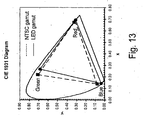
- The color gamut of any display apparatus is the area spanned between the color points of the red, green and blue pixels of the display in a chromaticity diagram, e.g. the CIE 1931 x, y diagram. The historical "golden standard" for displays is the NTSC gamut, defined by 3 sets of color point coordinates (x=0.674 and y=0.326 for red, x=0.218 and y=0.712 for green, and x=0.140 and y=0.080 for blue in the CIE 1931 x,y chromaticity diagram). Generally, a gamut greater than 70% of NTSC is considered acceptable for many backlighting applications, and a gamut greater than 90% of NTSC is considered acceptable for most any such application.
- In order to improve the gamut of LED backlights using yellow phosphors, the yellow light is filtered out, thereby reducing the effective LER of the LED backlight. It would be therefore beneficial to develop LED backlights that can provide LER of 280 Im/Wopt or greater at CCT>5000K without having yellow phosphors in the package. Red line-emitting phosphors would be particularly suitable for obtaining simultaneously such values for LER and CCT when used with blue or near-UV LED chips, in conjunction with at least a green-emitting and a blue-emitting phosphor, as needed.
- Other white light LED lighting systems use a UV or visible light LED chip along with a blend of red, green, and/or blue phosphors that can be efficiently excited by near-UV radiation to make white tight.
- The CRI is commonly defined as a mean value for 8 standard color samples (R1-8), usually referred to as the General Color Rendering Index and abbreviated as Ra, although 14 standard color samples are specified internationally and one can calculate a broader CRI (R1-14) as their mean value. In particular, the R9 value, measuring the color rendering for the strong red, is very important for a range of applications, especially of medical nature.
- As the CCT is lowered and/or the CRI is increased, the LER value generally decreases, leading to values for "warm white" LEDs (of CCT<4500K) significantly lower than those for "cool white" LEDs (of CCT>4500K). The LER value of any light source (including LEDs) can be improved by using red phosphors having a line emission spectrum, as opposed to red phosphors with a broadband emission. A significant portion of the emitted energy of the latter phosphors tends to fall into the deep red part of the spectrum where the sensitivity of the human eye is very low, thereby decreasing the LER value.
- In many lighting applications known in the art, phosphors with line emission spectra (e.g. Y2O3: Eu3+) are thus preferred as the red component because it maximizes LER at acceptable CRI values (e.g. 80-86), over the CCT range of interest (e.g. 3000-6500K). Current red fluorescent lamp phosphors doped with Eu3+ cannot be used successfully in UV LED lamps because they have virtually no absorption of near-UV (370-420 nm) light, leading to unacceptable light loss due to scattering by the phosphor. A deep red line emitting oxyfluoride phosphor, e.g. 3.5MgO*0.5MgF2*GeO2:Mn4+ (MFG) can be used in LED lamps, but with considerable impact to LER, due to much of its emission occurring too far in the red region of the spectrum (beyond 650 nm). Other similar phosphors based on oxide and oxyhalide host lattices doped with Mn4+ also have a main emission peak at a wavelength greater than 650 nm. It would be preferable to use red phosphors with line emission maxima at lower wavelengths, e.g. in the 610 to 650 nm range, capable of converting at least part of the radiation from the light source, e.g. an LED chip emitting in the UV to blue range. This improves the LER while maintaining the general CRI at 80 or above.
- Thus, a continuing need exists for new red line-emitting phosphors and their blends for use in display or lighting applications, particularly in conjunction with UV and visible LED chips displaying high quantum efficiency to produce white-light sources having both a high CRI and an improved LER at any given CCT, as well as backlights with minimal yellow emission and high LER.
- In a first aspect, there is provided a backlight emitting apparatus including a semiconductor light source; wherein the backlight comprises a red line-emitting phosphor having a peak emission wavelength between 610 and 650 nm; a green emitting phosphor having a peak emission wavelength between 510 and 550 nm; and either a) a blue LED chip having a peak emission wavelength between 440 and 480 nm, or b) a blue emitting phosphor having a peak emission wavelength between 440 and 480 nm and a violet to near-UV emitting LED chip having a peak emission wavelength from about 370 nm to about 440 nm. In a particular embodiment, a complex fluoride phosphor material activated with Mn4+ is used as the red line-emitting phosphor.
- In a second aspect, there is provided a light emitting apparatus including a light source and a complex fluoride phosphor material activated with Mn4+. In one embodiment, the complex fluoride phosphor may comprise at least one of: (A) A2[MF5]:Mn4+, where A is selected from Li, Na, K, Rb, Cs, NH4, and combinations thereof; and where M is selected from Al, Ga, In, and combinations thereof; (B) A3[MF6]:Mn4+, where A is selected from Li, Na, K, Rb, Cs, NH4, and combinations thereof; and where M is selected from Al, Ga, In, and combinations thereof; (C) Zn2[MF7]:Mn4+, where M is selected from Al, Ga, In, and combinations thereof; (D) A[In2F7]:Mn4+ where A is selected from Li, Na, K, Rb, Cs, NH4, and combinations thereof; (E) A2[MF6]:Mn4+, where A is selected from Li, Na, K, Rb, Cs, NH4, and combinations thereof; and where M is selected from Ge, Si, Sn, Ti, Zr, and combinations thereof; (F) E[MF6]:Mn4+, where E is selected from Mg, Ca, Sr, Ba, Zn, and combinations thereof; and where M is selected from Ge, Si, Sn, Ti, Zr, and combinations thereof; (G) Ba0.65Zr0.35F2.70:Mn4+; or (H) A3[ZrF7]:Mn4+ where A is selected from Li, Na, K, Rb, Cs, NH4, and combinations thereof.
- In a third aspect, there is provided a phosphor blend including at least one of the above complex fluoride phosphors activated with Mn4+ and at least one additional phosphor.
- In a fourth aspect, there is provided a phosphor material including at least one of: (A) A2[MF6]:Mn4+, where A is selected from Li, Na, K, Rb, Cs, NH4, and combinations thereof; and where M is selected from Sn, Zr, and combinations thereof; (B) E[MF6]:Mn4+, where E is selected from Mg, Ca, Sr, Ba, Zn, and combinations thereof; and where M is selected from Ge, Si, Sn, Ti, Zr, and combinations thereof; (C) Ba0.65Zr0.35F2.70:Mn4+; (D) A3[ZrF7]:Mn4+ where A is selected from Li, Na, K, Rb, Cs, NH4, and combinations thereof; (E) A2[MF6]:Mn4+, where A is selected from at least two among Li, Na, K, Rb, Cs, and NH4, and where M is selected from Ge, Si, Sn, Ti, Zr, and combinations thereof;
-
FIGURE 1 is a schematic cross-sectional view of an illumination system in accordance with one embodiment of the present invention. -
FIGURE 2 is a schematic cross-sectional view of an illumination system in accordance with a second embodiment of the present invention. -
FIGURE 3 is a schematic cross-sectional view of an illumination system in accordance with a third embodiment of the present invention. -
FIGURE 4 is a cutaway side perspective view of an illumination system in accordance with a fourth embodiment of the present invention. -
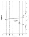
FIGURE 5 is a graph of the emission spectrum of a Na2[TiF6]:Mn4+ phosphor. -
FIGURE 6 is a graph of the emission spectrum of a K2[SnF6]:Mn4+ phosphor. -
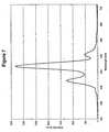
Figure 7 is a graph of the emission spectrum of a Ba[TiF6]:Mn4+ phosphor. -
FIGURE 8 is a graph of the emission spectrum of a K3[ZrF7]:Mn4+ phosphor. -
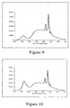
FIGURE 9 is the power distribution spectrum of an LED device using a present embodiment phosphor blend. -
FIGURE 10 is the power distribution spectrum of a second LED device using a present embodiment phosphor blend. -
FIGURE 11 is a graph of the excitation and emission spectra of a K3[AlF6]:Mn4+ phosphor according to an embodiment of the present invention. -
FIGURE 12 is an experimental spectral power distribution of a LED using blue chip and a blend of the phosphors K2[TiF6]:Mn4+ and STG. -
FIGURE 13 is a graphical representation of the gamuts of the NTSC standard and of a LED using blue chip and a blend of the phosphors K2[TiF6]:Mn4+ and STG in the CIE 1931 x, y chromaticity diagram. -
FIGURE 14 is a schematic perspective view of a surface mounted device (SMD) backlight LED. - Phosphors convert radiation (energy) to visible light. Different combinations of phosphors provide different colored light emissions. Novel phosphor compositions and blends are presented herein as well as their use in LED and other light sources.
- The color of the generated visible light is dependent on the particular components of the phosphor material. The phosphor material may include only a single phosphor composition or two or more phosphors of basic color, for example a particular mix with one or more of a yellow and red phosphor to emit a desired color (tint) of light. As used herein, the terms "phosphor" and "phosphor material" may be used to denote both a single phosphor composition as well as a blend of two or more phosphor compositions.
- It was determined that an apparatus that produces light containing a red line component by using a phosphor material capable of converting at least part of the radiation from a light source into red line emission having a peak wavelength between 610 and 650 nm would be useful e.g. in display or general lighting applications. A highly suitable example of such phosphor material is a complex fluoride phosphor activated with Mn4+. Referred examples for various embodiments will be provided further below.
- One or more additional phosphors can be used in conjunction with the above red line emitting phosphor in the phosphor material. Therefore, in one embodiment, a luminescent conversion material blend (phosphor blend) coated LED chip is disclosed for providing white light. The phosphor blends presented in this embodiment enable white light with an optimal combination of CRI and LER at any CCT of interest, when excited by radiation from about 250 to 550 nm as emitted by a near UV to green LED, either alone or in combination with any residual bleed from the LED.
- With reference to
Figure 1 , an exemplary LED based light emitting assembly orlamp 10 is shown in accordance with one preferred structure of the present invention. Thelight emitting assembly 10 comprises a semiconductor UV or visible radiation source, such as a light emitting diode (LED)chip 12 and leads 14 electrically attached to the LED chip. The leads 14 may comprise thin wires supported by a thicker lead frame(s) 16 or the leads may comprise self-supported electrodes and the lead frame may be omitted. The leads 14 provide current to theLED chip 12 and thus cause theLED chip 12 to emit radiation. - The lamp may include any semiconductor visible or UV light source that is capable of producing white light when its emitted radiation is directed onto the phosphor. The preferred peak emission of the LED chip in the present invention will depend on the identity of the phosphors in the disclosed embodiments and may range from, e.g., 250-550 nm. In one preferred embodiment, however, the emission of the LED will be in the near UV to blue-green region and have a peak wavelength in the range from about 370 to about 500 nm. Typically then, the semiconductor light source comprises an LED doped with various impurities. Thus, the LED may comprise a semiconductor diode based on any suitable III-V, II-VI or IV-IV semiconductor layers and having a peak emission wavelength of about 250 to 550 nm.
- Preferably, the LED may contain at least one semiconductor layer comprising GaN, ZnO or SiC. For example, the LED may comprise a nitride compound semiconductor represented by the formula IniGajAlkN (where 0≤i; 0≤j; 0≤k and i+j+k =1) having a peak emission wavelength greater than about 250 nm and less than about 550 nm. Such LED semiconductors are known in the art. The radiation source is described herein as an LED for convenience. However, as used herein, the term is meant to encompass all semiconductor radiation sources including, e.g., semiconductor laser diodes.
- Although the general discussion of the exemplary structures of the invention discussed herein are directed toward inorganic LED based light sources, it should be understood that the LED chip may be replaced by an organic light emissive structure or any other radiation source unless otherwise noted and that any reference to LED chip or semiconductor is merely representative of any appropriate radiation source.
- The
LED chip 12 may be encapsulated within ashell 18, which encloses the LED chip and anencapsulant material 20. Theshell 18 may be, for example, glass or plastic. Preferably, theLED 12 is substantially centered in theencapsulant 20. Theencapsulant 20 is preferably an epoxy, plastic, low temperature glass, polymer, thermoplastic, thermoset material, resin or other type of LED encapsulating material as is known in the art. Optionally, theencapsulant 20 is a spin-on glass or some other material having a high index of refraction. In one embodiment, theencapsulant material 20 is a polymer material, such as epoxy, silicone, or silicone epoxy, although other organic or inorganic encapsulants may be used. Both theshell 18 and theencapsulant 20 are preferably transparent or substantially optically transmissive with respect to the wavelength of light produced by theLED chip 12 and a phosphor material 22 (described below). In an alternate embodiment, thelamp 10 may only comprise an encapsulant material without anouter shell 18. TheLED chip 12 may be supported, for example, by thelead frame 16, by the self supporting electrodes, the bottom of theshell 18, or by a pedestal (not shown) mounted to the shell or to the lead frame. - The structure of the illumination system includes a
phosphor material 22 radiationally coupled to theLED chip 12. Radiationally coupled means that the elements are associated with each other so that at least part of the radiation emitted from one is transmitted to the other. - This
phosphor material 22 is deposited on theLED 12 by any appropriate method. For example, a suspension of the phosphor(s) can be formed, and applied as a phosphor layer to the LED surface. In one such method, a silicone, epoxy or other matrix material is used (either directly or diluted with an organic solvent, e.g. acetone, MIBK or butyl acetate) to create a slurry in which the phosphor particles are randomly suspended and placed around the LED. This method is merely exemplary of possible positions of thephosphor material 22 andLED 12. Thus, thephosphor material 22 may be coated over or directly on the light emitting surface of theLED chip 12 by coating and drying or curing the phosphor suspension over theLED chip 12. Both theshell 18 and theencapsulant 20 should be transparent to allow light 24 to be transmitted through those elements. Although not intended to be limiting, the median particle size of the phosphor material as measured using light scattering methods or via microscope (electron or optical) measurements may be from about 1 to about 20 microns. -
FIG. 2 illustrates a second preferred structure of the apparatus according to the preferred aspect of the present invention. Corresponding numbers fromFigures 1-4 (e.g. 12 inFigure 1 and 112 inFigure 2 ) relate to corresponding structures in each of the figures unless otherwise stated. The structure of the embodiment ofFIG. 2 is similar to that ofFIG. 1 , except that thephosphor material 122 is interspersed within theencapsulant material 120, instead of being formed directly on theLED chip 112. The phosphor material (in the form of a powder) may be interspersed within a single region of theencapsulant material 120 or, more preferably, throughout the entire volume of the encapsulant material.Radiation 126 emitted by theLED chip 112 mixes with the light emitted by thephosphor material 122, and the mixed light appears aswhite light 124. If the phosphor is to be interspersed within theencapsulant material 120, then a phosphor powder may be added to a polymer precursor, loaded around theLED chip 112, and then the polymer precursor may be cured to solidify the polymer material. Other known phosphor interspersion methods may also be used, such as transfer molding. -
FIG. 3 illustrates a third preferred structure of the apparatus according to the preferred aspects of the present invention. The structure of the embodiment shown inFIG. 3 is similar to that ofFIG. 1 , except that thephosphor material 222 is coated onto a surface of theshell 218, instead of being formed over theLED chip 212. The phosphor material is preferably coated on the inside surface of theshell 218, although the phosphor may be coated on the outside surface of the shell, if desired. Thephosphor material 222 may be coated on the entire surface of the shell or only a top portion of the surface of the shell. Theradiation 226 emitted by theLED chip 212 mixes with the light emitted by thephosphor material 222, and the mixed light appears aswhite light 224. Of course, the structures ofFIGS. 1-3 may be combined and the phosphor may be located in any two or all three locations or in any other suitable location, such as separately from the shell or integrated into the LED. - In any of the above structures, the
lamp 10 may also include a plurality of scattering particles (not shown), which are embedded in the encapsulant material. The scattering particles may comprise, for example, Al2O3 particles (such as alumina powder) or TiO2 particles. The scattering particles effectively scatter the coherent light emitted from the LED chip, preferably with a negligible amount of absorption. - As shown in a fourth preferred structure in
Figure 4 , theLED chip 412 may be mounted in areflective cup 430. Thecup 430 may be made from or coated with a reflective material, such as alumina, titania, or other dielectric powder known in the art. A preferred reflective material is Al2O3. The remainder of the structure of the embodiment ofFIG. 4 is the same as that of any of the previous Figures, and includes twoleads 416, aconducting wire 432 electrically connecting theLED chip 412 with the second lead, and anencapsulant material 420. - Another preferred structure (particularly for backlight applications) is a surface mounted device ("SMD") type
light emitting diode 550, e.g. as shown inFIG. 14 . This SMD is of a "side-emitting type" and has alight emitting window 552 on a protruding portion of alight guiding member 554. The SMD typelight emitting diodes 550 can be made by disposing LEDs that have been formed beforehand by flow soldering or the like on a glass epoxy substrate, whereon an electrically conductive pattern has been formed and covering said LED with thewindow 552. There are also "top-emitting" SMD packages known in the art that are also suitable for use in the present embodiments, e.g. those produced by Nichia Corporation. An SMD package may comprise an LED chip as defined above, and a phosphor material as discussed below that is excited by the light emitted from the LED chip. - In one embodiment, there is provided a novel phosphor material, which may be used in the phosphor composition in the above described devices. The phosphor material is a complex fluoride phosphor activated with Mn4+ and may comprise one or more of (A) A2[MF5]:Mn4+, where A is selected from Li, Na, K, Rb, Cs, NH4, and combinations thereof; and where M is selected from Al, Ga, In, and combinations thereof; (B) A3[MF6]:Mn4+, where A is selected from Li, Na, K, Rb, Cs, NH4, and combinations thereof; and where M is selected from Al, Ga, ln, and combinations thereof; (C) Zn2[MF7]:Mn4+, where M is selected from Al, Ga, ln, and combinations thereof; (D) A[In2F7]:Mn4+ where A is selected from Li, Na, K, Rb, Cs, NH4, and combinations thereof: (E) A2[MF6]:Mn4+, where A is selected from Li, Na, K, Rb, Cs, NH4, and combinations thereof; and where M is selected from Sn, Zr, and combinations thereof; (F) E[MF6]:Mn4+, where E is selected from Mg, Ca, Sr, Ba, Zn, and combinations thereof; and where M is selected from Sn, Zr, and combinations thereof; (G) Ba0.65Zr0.35F2.70:Mn4+; (H) A3[ZrF7]:Mn4+ where A is selected from Li, Na, K, Rb, Cs, NH4, and combinations thereof; (I) A2[MF6]:Mn4+, where A is selected from at least two among Li, Na, K, Rb, Cs, and NH4, and where M is selected from Ge, Si, Sn, Ti, Zr, and combinations thereof; or (J) A2[MF6]:Mn4+, where A is selected from Li, Na, K, Rb, Cs, NH4, and combinations thereof, and where M is selected from at least two among Ge, Si, Sn, Ti, and Zr.
- By "complex fluoride phosphor", it is meant that the phosphor is a coordination compound, containing at least one coordination center (e.g. M in the examples above), surrounded by fluoride ions acting as ligands, and charge-compensated by counter ions (e.g. A in the examples above) as necessary. Complex fluorides are occasionally written down as a combination of simple, binary fluorides (e.g.3NaF.AlF3 instead of Na3[AlF6]), but such a representation does not indicate the coordination number (in this example, 6) for the ligands around the coordination center. The square brackets (occasionally omitted for simplicity) indicate that the complex ion they encompass is a new chemical species, different from the simple fluoride ion. The activator ion (Mn4+) also acts as a coordination center, substituting part of the centers of the host lattice, e.g. Al3+. The host lattice (including the counter ions) can further modify the excitation and emission properties of the activator ion.
- When used with an LED chip having a peak emission from 250 to 550 nm and one or more additional phosphors (such as blue and green emitting phosphors), the use of the above phosphor material allows for a white LED. The additional phosphors that can be used are described in more detail below.
- Exemplary Mn4+ activated compositions of this embodiment are detailed below in Table 1.
Table 1 ID# Phosphor Raw materials 1 K2[AlF5]:Mn4+ Al(OH)3, K2CO3 K7[MnF6] 2 K3[AlF6]:Mn4+ Al(OH)3, K2CO3 K2[MnF6] 3 K3[GaF6]:Mn4+ Ga2O3, K2CO3 K2[MnF6] 4 Zn2[AF7]:Mn4+ ZnO, Al(OH)3 K2[MnF6] 5 K[n2F7]:Mn4+ In2O3, K2CO3 K2[MnF6] 6 K2[SiF6]:Mn4+ K2[SiF6] K2[MnF6] 7 K2[TiF6]:Mn4+ K2[TiF6] K2[MnF6] 8 K3[ZrF7]:Mn4+ K3[ZrF7] K2[MnF6] 9 Ba0.65Zr0.35F2.70: Mn4+ Zr(OH)4 BaCO3 K2[MnF6] 10 Ba[TiF6]:Mn4+ TiO2 BaCO3 K2[MnF6] 11 K2[SnF6]:Mn4+ K2SnO3. 3H2O K2[MnF6] 12 Na2TiF6]:Mn4 Na2[TiF6] K2[MnF6] 13 Na2[ZrF6]:Mn4+ Na2[ZrF6] K2[MnF6] 14 KRb[TiF6]:Mn4+ K2[TiF6], Rb2[TiF6] K2[MnF6] 15 K2[Si0.5Ge0.5F6]:Mn4+ SiO2, GeO2, K2CO3 K2[MnF6] - Complex fluoride phosphors doped with Mn4+ with a coordination number of 6 for the coordination center (i.e. in a generally octahedral environment, as in K2[TiF6]:Mn4+) are particularly preferred. Other complex fluorides with higher coordination numbers for the central ion (e.g. K3[ZrF7] with a coordination number of 7) are also applicable as host lattices for activation with Mn4+.
- Advantageously, more than one cation can be used in the host lattice (e.g. as shown in
Row # 14 of Table 1 above and in Example 10 below), to optimize the quantum efficiency of the phosphor. Further, more than one coordination center can be used in the host lattice (e.g. as shown in Row #15 of Table 1 above and in Example 11 below), to broaden the excitation spectrum of the phosphor, thereby making it more suitable for practical use, e.g. with a broader range of LED chips. Preferably, at least two cations and/or at least two coordination centers will be used to optimize the quantum efficiency and the excitation spectrum of the phosphor. -
Figures 5-8 show the emission spectra of several of these phosphors when excited by 365 nm UV light. That is,Figure 5 is a graph of the emission spectrum of a Na2[TiF6]:Mn4+ phosphor.Figure 6 is a graph of the emission spectrum of a K2[SnF6]:Mn4+ phosphor.Figure 7 is a graph of the emission spectrum of Ba[TiF6]:Mn4+ phosphor.Figure 8 is a graph of the emission spectrum of a K3[ZrF7]:Mn4+ phosphor.Figure 11 shows the excitation and emission spectra of a K3[AlF6]:Mn4,1 phosphor. - The above described complex fluoride phosphor compositions activated with Mn4+ can be prepared by taking appropriate raw materials in a ratio sufficient to ensure the desired incorporation level of the activator ion (e.g. between 0.1 and 30 mol.% of the total M content, more preferably between 2 and 15 mol%). In one embodiment, the raw materials may be dissolved together in aqueous hydrofluoric acid (e.g. 30 to 50% HF by weight) and the phosphor is produced by evaporation of the reaction mixture to dryness in a plastic or Teflon-lined vessel, preferably with continuous heating below the boiling point of the solution - e.g. on a water bath. The crude phosphor may be then milled (preferably dry-milled) to a desired particle size, washed with an organic solvent (e.g. ethanol or acetone) to remove any remaining amounts of HF and dried on the air prior to use in LEDs.
- A variety of other starting materials and processes may be used to produce the complex fluoride phosphors in this embodiment via co-crystallization from aqueous solution of HF and/or other fluorides (e.g. prepared in-situ or ex-situ from oxides, hydroxides, alkoxides, carbonates and binary fluorides or hydrogen fluorides of the metal constituents), and permanganates, or manganates with a stoichiometric amount of H2O2 or other peroxide to provide the Mn activator in the proper oxidation state (+4). The examples of complex fluoride phosphors doped with Mn4+ shown herein are not meant to be limiting. Other constituent ions may be used to build the complex fluoride host lattice (as the coordination center or the counter ion), provided they do not introduce electronic or vibrational transitions deleterious to the phosphor excitation and/or emission upon activation with Mn4+.
- The relative amounts of each phosphor in the phosphor material can be described in terms of spectral weight. The spectral weight is the relative amount that each phosphor contributes to the overall emission spectra of the phosphor blend. The spectral weight amounts of all the individual phosphors should add up to 1. A preferred blend comprises a spectral weight of from 0.01 to 0.80 of a phosphor having a peak emission of from about 500 to 610 nm, from 0 to 0.19 of an optional phosphor having a peak emission from about 430 to 500 nm (which would not be needed for excitation with a blue or blue-green LED having a peak emission from about 430 to about 500 nm), and the balance of the blend being one of the above described complex fluoride phosphors, as needed to achieve the targeted CCT value. Any known phosphors suitable for use in near-UV to green LED systems and emitting in the above wavelength ranges may be used. Garnets activated with at least Ce3+ (e.g. YAG:Ce, TAG:Ce and their compositional modifications known in the art) are particularly preferred phosphors with a peak emission at about 500 to 610 nm. Other particularly preferred phosphors having a peak emission in the latter range are alkaline earth silicates activated with at least Eu2+, e.g. (Ba,Sr,Ca)2SiO4: Eu2+ ("BOS") and its compositional modifications known in the art.
- It should be noted that various phosphors are described herein in which different elements enclosed in parentheses and separated by commas, such as in the case of (Ba,Sr,Ca)2SiO4: Eu2+. As understood by those skilled in the art, this type of notation means that the phosphor can include any or all of those specified elements in the formulation in any ratio. That is, this type of notation for the above phosphor, for example, has the same meaning as (Baasrbca1-a-b)2SiO4: Eu2+, where a and b can vary from 0 to 1, including the values of 0 and 1.
- As detailed above, an LED backlight device or apparatus may also be produced. As used herein, the terms "device" and "apparatus" are meant to include not only a single LED light or backlight, but also the arrangement of two or more LED backlights on a circuit board or in another type of array.
- A red line-emitting phosphor having a peak emission wavelength between 610 and 650 nm may be used to prepare an LED backlight device, in conjunction with at least a green emitting phosphor (e.g. with a peak emission wavelength between 510 and 550 nm) and either a blue LED chip or a blue emitting phosphor (e.g. with a peak emission wavelength between 440 and 480 nm) and a violet to near-UV emitting LED chip (e.g. having a peak emission wavelength from about 370 nm to about 440 nm).
- Advantageously, virtually any complex fluoride phosphor activated with Mn4+ is a suitable example for said red line-emitting phosphor. Non-limiting examples of suitable red line emitting phosphors include the phosphors described herein, as well as those described in parent applications
U.S. Patent Applications Nos. 11/364,611 ,11/049,598 11/285,442 - Backlights made with complex fluoride phosphor activated with Mn4+ can have LER equivalent or better than that of typical blue chip/yellow phosphor LEDs (e.g. greater than 280 Im/Wopt at CCTs higher than 5000K). However, unlike the yellow phosphor based LEDs, they will have very little emission in the yellow region of the spectrum which is undesirable for backlighting applications, as explained earlier. Preferably, such backlights will have a gamut greater than 70% that of the NTSC standard, and more preferably greater than 90% that of the NTSC standard in the CIE 1931 x, y diagram.
- The spectrum of an experimental LED having a CCT of 2900K, Ra of 82 and LER of 342 Im/Wopt is shown in
Fig. 9 . The spectrum of a second experimental LED having a CCT of 3500K, Ra of 92 and LER of 312 Im/Wopt is shown inFigure 10 . Both of these LEDs use a blue chip with a terbium aluminum garnet phosphor activated with Ce3+ (Tb2.91Ce0-09Al4.90O11.85) and a red line emitting complex fluoride phosphor (K2TiF6]:Mn4+). - The experimental spectrum of another LED using a blue chip and a blend of the phosphors K2[TiF6]:Mn4+ and STG is shown in
Fig. 12 . It has chromaticity coordinates x=0.315 and y=0.335 (corresponding to a CCT of 6300K), LER of 292 Im/Wopt and a gamut 101% that of NTSC in the CIE 1931 x, y diagram, as shown graphically inFig. 13 . - In addition, other phosphors emitting throughout the visible spectrum region, at wavelengths substantially different from those of the phosphors described in the present invention, may be used in the blend to customize the color of the resulting light and produce sources with improved light quality. While not intended to be limiting, suitable phosphors for use in the blend with the present phosphors include:
- (Ba,Sr,Ca)5(PO4)3(Cl,F,Br,OH):Eu2+,Mn2+
- (Ba,Sr,Ca)BPO5:Eu2+,Mn2+
- (Sr,Ca)10(PO4)6*νB2.3:Eu2+ (wherein 0<v≤1)
- Sr2Si3O8*2SrCl2:Eu2+
- (Ca,Sr,Ba)3MgSi2O8:Eu2+,Mn2+
- BaAl8O13:Eu2+
- 2SrO*O.84P2O5*0.16B2O3:Eu2+,
- (Ba,Sr,Ca)MgAl10O17:Eu2+,Mn2+
- (Ba,Sr,Ca)Al2O4:Eu2+
- (Y,Gd,Lu,Sc,La)BO3:Ce3+,Tb3+
- (Ba,Sr,Ca)2Si1-ξO4-2ξ:Eu2+ (wherein 0≤ξ≤0.2)
- (Ba,Sr,Ca)2(Mg,Zn)Si2O7:Eu2+
- (Sr,Ca,Ba)(Al,Ga,In)2S4:Eu2+
- (Y,Gd,Tb,La,Sm,Pr, LU)3(SC,Al,Ga)5-aO12-3/2a·Ce3+ (wherein 0≤α≤0.5)
- (Lu,Sc,Y,Tb)2-u-vCevCa1+uLiwMg2-wPw(Si,Ge)3-wO12-u/2 where -0.5≤u≤1; 0<v≤0.1; and 0≤w≤0.2
- (Ca,Sr)8(Mg,Zn)8SiO4)4Cl2:Eu2+,Mn2+
- Na2Gd2B2O7:Ce3+,Tb3+
- (Sr,Ca,Ba,Mg,Zn)2P2O7:Eu2+,Mnz+
- (Gd,Y,Lu,La)2O3:Eu3+,Bi3+
- (Gd,Y,Lu,La)2O2S:Eu3+,Bi3+
- (Gd,Y,Lu,La)VO4:Eu3+,Bi3+
- (Ca,Sr)S:Eu2+,Ce3+
- ZnS:Cu+,Cl-
- ZnS:Cu+,Al3+
- ZnS:Ag+,Cl-
- ZnS:Ag+,Al3+
- SrY2S4:Eu2+
- CaLa2S4:Ce3+
- (Ba,Sr,Ca)MgP2O7:Eu2+,Mn2+
- (Y,Lu)2WO6:Eu3+,Mo6+
- (Ba,Sr,Ca)βSiyNµ:Eu2+ (wherein 2β+4y=3µ)
- Ca3(SiO4)Cl2:Eu2+
- (Y,Lu,Gd)2-ϕCaϕSi4N6+ϕC1-ϕ:C1-ϕCe3+, (wherein 0≤ϕ≤0.5)
- (Lu,Ca,Li,Mg,Y)aipha-SiAlON doped with Eu2+ and/or Ce3+
- (Ca,Sr,Ba)SiO2N2:Eu2+,Ce3+
- 3.5MgO*0.5MgF2*GeO2:Mn4+
- Ca1-c-fCecEufAl1+cSi1-cN3, (where 0<c≤0.2, 0≤f≤0.2)
- Ca1-h-rCehEurAl1-h(Mg,Zn)hSiN3, (where 0<h≤0.2, 0≤r≤0.2)
- Ca1-2s-tCes(Li,Na)sEutAISiN3, (where 0≤s≤0.2, 0≤f≤0.2, s+t>0)
- Ca1-σ-χ-φCeσ(Li,Na)χEuφAl1+σ-χSi1-σ+χN3, (where 0≤σ≤0.2, 0<χ≤0.4, 0≤φ≤0.2)
- For purposes of the present application, it should be understood that when a phosphor has two or more dopant ions (i.e. those ions following the colon in the above compositions), this is to mean that the phosphor has at least one (but not necessarily all) of those dopant ions within the material. That is, as understood by those skilled in the art, this type of notation means that the phosphor can include any or all of those specified ions as dopants in the formulation.
- When the phosphor composition includes a blend of two or more phosphors, the ratio of each of the individual phosphors in the phosphor blend may vary depending on the characteristics of the desired light output. The relative proportions of the individual phosphors in the various embodiment phosphor blends may be adjusted such that when their emissions are blended and employed in an lighting device, there is produced visible light of predetermined x and y values on the CIE chromaticity diagram. As stated, a white light is preferably produced. This white light may, for instance, may possess an x value in the range of about 0.30 to about 0.55, and a y value in the range of about 0.30 to about 0.55. Preferably, the color point of the white light will lie on or substantially on the Planckian (also known as the blackbody) locus, e.g. within 0.020 units in the vertical (y) direction of the
CIE 1931 chromaticity diagram, more preferably within 0.010 units in the vertical direction. As stated, however, the identity and amounts of each phosphor in the phosphor composition can be varied according to the needs of the end user. Since the efficiency of individual phosphors may vary widely between suppliers, the exact amounts of each phosphor needed are best determined empirically, e.g. through standard design of experiment (DOE) techniques. - It may be desirable to add pigments or filters to the phosphor composition. When the LED is a UV emitting LED, the
phosphor layer 22 may also comprise from 0 up to about 10 % by weight (based on the total weight of the phosphors) of a pigment or other UV absorbent material capable of absorbing or reflecting UV radiation having a wavelength between 200 nm and 450 nm. - Suitable pigments or filters include any of those known in the art that are capable of absorbing radiation generated between 200 nm and 450 nm. Such pigments include, for example, nickel titanate or praseodymium zirconate. The pigment may be used in an amount effective to filter 10% to 100% of the radiation generated in the 200 nm to 500 nm range.
- The raw materials (18.48g of K2[TiF6], obtained commercially from Fluka and 1.52 g of K2[MnF6], prepared according to Bode's method [H.Bode, H.Jenssen, F. Bandte, Angew. Chem., N11(1953), 304] were dissolved in 200 ml of aqueous 40% HF while stirring under heating. The solution was evaporated in a plastic dish on a water bath to dryness. As noted above with reference to
Figures 9 and 10 , LEDs using a blue chip with a terbium aluminum garnet activated with Ce3+ (Tb2.91Ce0-09Al4.90O11.85) and the present red line emitting phosphor (K2[TiF6]:Mn4+) were produced. - K2[MnF6] (1.34g) was dissolved in 100 ml of aqueous 40% HF with stirring, followed by TiO2 hydrate (prepared by hydrolysis of tetraisopropyl orthotitanate in distilled water and equivalent to 4.90 g of pure TiO2 according to the loss on ignition method). Solid BaCO3 (12.30 g) was then added gradually to the stirred solution. The resulting suspension was evaporated to dryness on a water bath.
- The raw materials (9.64 g of manufactured K3[ZrF7] and 0.36 g of K2[MnF6]) were dissolved in 100 ml of aqueous 40% HF while stirring, under heating. The solution was evaporated in a plastic dish on a water bath to dryness.
- Solid BaCO3 (11.52 g) and Zr(OH)4 (9.30 g) were added gradually to 200 ml of aqueous 40% HF with stirring . The slurry was heated for 30 min. on a water bath. The resulting precipitate of Ba0.55 Zr0.35 F2.70 was washed with deionized water through decantation until neutral pH and dried at 100°C. K2[MnF6] (1.13 g) was dissolved in 200 ml of aqueous 40% HF suspension of Ba0.65 Zr0.35 F2.70 (18.87 g) while stirring and then heated on a water bath until a dry residue was formed.
- The raw materials (3.52 g of Al(OH)3 and 6.23 g of K2CO3) are dissolved by careful gradual addition into 40 ml of 50% aqueous HF under heating and stirring of the Teflon dish on a hot plate. The solution is evaporated to dryness to form the K2[AlF5] host complex, which is then dissolved in 50 ml of 50% HF along with 0.97 g of K2[MnF6], prepared according to Bode's method [H. Bode, H. Jenssen, F. Bandte, Angew. Chem., N11(1953), 304] while stirring under heating. The second solution is evaporated on a water bath to dryness.
- For this phosphor, 2.79 g of AI(OH)3 and 7.41 g of K2CO3 are dissolved by careful gradual addition into 40 ml of 50% aqueous HF under heating and stirring of the Teflon dish on a hot plate. The solution is evaporated to dryness to form the K3[AlF6] host complex, which is then dissolved in 50 ml of 50% HF along with 0.77 g of K2[MnF6] and evaporated on a water bath to dryness.
- This preparation is carried in the same manner as in the previous example, using 2.91 g of Ga2O3 and 6.43 g of K2CO3 in the first step (dissolution in 50 ml of 50% HF), followed by 0.67 g of K2[MnF6] in the second step.
- This phosphor is prepared by dissolving 2.57g of Al(OH)3 and 0.34 g of K2[MnF6] into 50 ml of 45% HF and the solution is heated to 60oC on a water bath. Then 5.37 g of ZnO is added slowly in small portions, and the formed solution is evaporated to dryness.
- A 6.91 g sample of In2O3 is dissolved in 100 ml of 50% HF with heating on a water bath and 3.44 g of K2CO3 is then added gradually in small portions. The solution is evaporated to dryness on a water bath and the excess KF is removed by precipitation with 100 ml ethanol, followed by filtration. The filtrate is collected, evaporated to dryness and dissolved in 50 ml of 40% HF under heating and stirring, along with 0.51 g of K2[MnF6]. The final solution is again evaporated to dryness.
- The following amounts of materials: 5.40 g of Rb2[TiF6] (prepared by dissolving 2.40 g of TiO2 into 50 ml of 40% HF followed by 6.94 g of Rb2CO3 added gradually at room temperature, crystallizing via addition of 100 ml absolute ethanol, washing the precipitate with ethanol and then drying it at 100 °C), 3.90 g of K2[TiF6] (either prepared in a similar fashion e.g. from 3.33 g of TiO2 and 5.76 g of K2CO3 or obtained commercially), and 0.70 g of K2[MnF6] is dissolved in 100 ml of 40% HF. The solution is then evaporated to dryness at 100 °C.
- The following amounts of materials: 1.24 g of fumed silica (e.g. Aerosil) and 2.16 g of GeO2 are dissolved in 100 ml of 40% HF on a hot bath with stirring. Then 5.70 g of K2CO3 are added carefully in small portions and the reaction mixture is evaporated to dryness. The dry residue is re-dissolved in 100 ml of 40% HF on a hot bath with stirring, and 0.89 g of K2[MnF6] is added to the solution. The final solution is then evaporated to dryness at 100 °C.
- Apart from white light blends for general illumination, these phosphors can be used either individually or in blends for LEDs for traffic signals, signage, and particularly for LCD backlighting applications. The narrow red line emission allows for a saturated color that is highly desirable for these applications.
- The phosphor materials described above may be used in additional applications besides LEDs. For example, the material may be used as a phosphor in a fluorescent lamp, in a cathode ray tube, in a plasma display device or in a liquid crystal display (LCD). These uses are meant to be merely exemplary and not exhaustive.
- The present development has been described with reference to various exemplary embodiments. Modifications and alteration will occur to others upon a reading and understanding of this specification. The invention is intended to include all such modifications and alterations insofar as they come within the scope of the appended claims or the equivalent thereof.
Claims (12)
- A lighting apparatus for emitting light comprising:a light source; anda phosphor material radiationally coupled to the light source and capable of converting at least a portion of the radiation emitted by the light source into light having a peak emission wavelength between 610 and 650 nm, the phosphor material comprising a complex fluoride phosphor activated with Mn4+.
- The lighting apparatus of claim 1, wherein said complex phosphor comprises at least one phosphor selected from the group consisting of:(A) A2[MF5]:Mn4+, where A is selected from Li, Na, K, Rb, Cs, NH4, and combinations thereof; and where M is selected from Al, Ga, In, and combinations thereof;(B) A3[MF6]:Mn4+, where A is selected from Li, Na, K, Rb, Cs, NH4, and combinations thereof; and where M is selected from Al, Ga, In, and combinations thereof;(C) Zn2[MF7]:Mn4+, where M is selected from Al, Ga, In, and combinations thereof;(D) A[In2F7]:Mn4+ where A is selected from Li, Na, K, Rb, Cs, NH4, and combinations thereof;(E) A2[MF6]:Mn4+, where A is selected from Li, Na, K, Rb, Cs, NH4, and combinations thereof; and where M is selected from Ge, Si, Sn, Ti, Zr, and combinations thereof;(F) E[MF6]:Mn4+, where E is selected from Mg, Ca, Sr, Ba, Zn, and combinations thereof; and where M is selected from Ge, Si, Sn, Ti, Zr, and combinations thereof;(G) Ba0.65Zr0.35F2.70:Mn4+; and(H) A3[ZrF7]:Mn4+ where A is selected from Li, Na, K, Rb, Cs, NH4, and combinations thereof.
- The lighting apparatus of claim 1, wherein the light source is a semiconductor light emitting diode (LED) emitting radiation having a peak wavelength in the range of from about 370 to about 500 nm.
- The lighting apparatus of claim 1, wherein the light source is an organic emissive structure.
- The lighting apparatus of claim 1, wherein said phosphor material further comprises one or more additional phosphors.
- The lighting apparatus of claim 5, wherein said one or more additional phosphors is one or more of a garnet activated with Ce3+ or an alkaline earth silicate activated with Eu2+.
- The lighting apparatus of claim 5, wherein said one or more additional phosphors are selected from the group including: (Ba,Sr,Ca)5(PO4)3(C),F,Br,OH):Eu2+,Mn2+; (Ba,Sr,Ca)BPO5: Eu2+, Mn2+; (Sr,Ca)10(PO4)6*νB2O3:Eu2+ (wherein 0<ν≤1); Sr2Si3O8*2SrCl2:EU2+; (Ca,Sr,Ba)3MgSi2O8:Eu2+,Mn2+; BaAl8O13:Eu2+; 2SrO*0.84P2O5*0.16B2O3:Eu2+; (Ba,Sr,Ca)MgAl10O17:Eu2+,Mn2+; (Ba,Sr,Ca)Al2O4:Eu2+; (Y,Gd,Lu,Sc,La)BO3:Ce3+,Tb3+; ZnS:Cu+,Cl-; ZnS:Cu+,Al3+; ZnS:Ag+,Cl; ZnS:Ag+,Al3+; (Ba,Sr,Ca)2Si1-ξO4-2ξ:Eu2+ (wherein 0≤ξ≤0.2); (Ba,Sr,Ca)2(Mg,Zn)Si2O7:Eu2+; (Sr,Ca,Ba)(Al,Ga,In)2S4:EU2+; (Y,Gd,Tb,La,Sm,Pr,Lu)3(Al,Ga)5-αO12-3/2α:Ce3+ (wherein 0≤α≤0.5); (Ca,Sr)8(Mg,Zn)(SiO4)4Cl2:Eu2+,Mn2+; Na2Gd2B2O7:Ce3+,Tb3+; (Sr,Ca,Ba,Mg,Zn)2P2O7:Eu2+,Mn2+; (Gd,Y,Lu,La)2O3Eu3+,Bi3+; (Gd,Y,Lu,La)2O2S:Eu3+,Bi3+; (Gd,Y,Lu,La)V04:Eu3+,Bi3+; (Ca,Sr)S:Eu2+,Ce3+; SrY2S4:Eu2+; CaLa2S4:Ce3+; (Ba,Sr,Ca)MgP2O7:Eu2+,Mn2+; (Y,Lu)2WO6:Eu3+,MO6+; (Ba,Sr,Ca)βSiγNµ:Eu2+ (wherein 2β+4γ=3µ); Ca3(SiO4)Cl2:Eu2+; (Lu,Sc,Y,Tb)2-u-vCevCa1+uLiwMg2-wPw(Si,Ge)3-wO12O12-u/2 (where -0.5≤u≤1, 0<v≤0.1, and 0≤w≤0.2); (Y,Lu,Gd)2-ϕCaϕSi4N6+ϕC1-ϕ:Ce3+, (wherein 0≤ϕ≤0.5); (Lu,Ca,Li,Mg,Y)alpha-SiAION doped with Eu2+ and/or Ce3+; (Ca,Sr,Ba)SiO2N2:Eu2+,Ce3+; 3.5MgO*0.5MgF2*GeO2:Mn4+; Ca1-c-fCecEufAlfAl1+cSi1-cN3, (where 0<c≤0.2, 0≤f≤0.2); Ca1-h-rCehEurAl1-h(Mg,Zn)hSiN3, (where 0<h≤0.2, 0≤r≤0.2); Ca1-2s-tCes(Li, Na)sEutAlSiN3, (where 0≤s≤0.2, 0≤f≤0.2, s+t>0); and Ca1-σ-χ-φCeσ(Li,Na)χEuφAl1+σ+χN3, (where 0≤σ≤0.2, 0<χ≤0.4, 0≤φ≤0.2).
- The lighting apparatus of claim 1, having a white light with a CCT of less than 4500K.
- The lighting apparatus of claim 8, where said white light has a general CRI greater than 90.
- The lighting apparatus of claim 8, where said white light has a LER greater than 330 Im/Wopt.
- A phosphor material comprising at least one phosphor selected from the group consisting of:(A) A2[MF6]:Mn4+, where A is selected from Li, Na, K, Rb, Cs, NH4, and combinations thereof; and where M is selected from Sn, Zr, and combinations thereof;(B) E[MF6]:Mn4+, where E is selected from Mg, Ca, Sr, Ba, Zn, and combinations thereof; and where M is selected from Ge, Si, Sn, Ti, Zr, and combinations thereof;(C) Ba0.65Zr0.35F2.70:Mn4+;(D) A3[ZrF7]:Mn4+ where A is selected from Li, Na, K, Rb, Cs, NH4, and combinations thereof; and(E) A2[MF6]:Mn4+, where A is selected from at least two among Li, Na, K, Rb, Cs, and NH4, and where M is selected from Ge, Si, Sn, Ti, Zr, and combinations thereof.
- A backlight apparatus comprising a red line-emitting complex fluoride phosphor material activated with Mn4+ having a peak emission wavelength between 610 and 650 nm; a green emitting phosphor having a peak emission wavelength between 510 and 550 nm; and either a) a blue LED chip having a peak emission wavelength between 440 and 480 nm, or b) a blue emitting phosphor having a peak emission wavelength between 440 and 480 nm and a violet to near-UV emitting LED chip having a peak emission wavelength from about 370 nm to about 440 nm.
Applications Claiming Priority (2)
| Application Number | Priority Date | Filing Date | Title |
|---|---|---|---|
| US11/364,611 US7497973B2 (en) | 2005-02-02 | 2006-02-28 | Red line emitting phosphor materials for use in LED applications |
| PCT/US2007/005083 WO2007100824A2 (en) | 2006-02-28 | 2007-02-26 | Red line emitting phosphors for use in led applications |
Publications (2)
| Publication Number | Publication Date |
|---|---|
| EP1999230A2 EP1999230A2 (en) | 2008-12-10 |
| EP1999230B1 true EP1999230B1 (en) | 2012-06-13 |
Family
ID=38357972
Family Applications (1)
| Application Number | Title | Priority Date | Filing Date |
|---|---|---|---|
| EP07751816A Active EP1999230B1 (en) | 2006-02-28 | 2007-02-26 | Red line emitting phosphors for use in led applications |
Country Status (4)
| Country | Link |
|---|---|
| US (1) | US7497973B2 (en) |
| EP (1) | EP1999230B1 (en) |
| JP (4) | JP5715327B2 (en) |
| WO (1) | WO2007100824A2 (en) |
Cited By (1)
| Publication number | Priority date | Publication date | Assignee | Title |
|---|---|---|---|---|
| CN104357050A (en) * | 2014-10-25 | 2015-02-18 | 云南民族大学 | High-color-purity red luminescent material for blue light excitation and preparation method of red luminescent material |
Families Citing this family (214)
| Publication number | Priority date | Publication date | Assignee | Title |
|---|---|---|---|---|
| US7648649B2 (en) * | 2005-02-02 | 2010-01-19 | Lumination Llc | Red line emitting phosphors for use in led applications |
| US7859182B2 (en) * | 2005-08-31 | 2010-12-28 | Lumination Llc | Warm white LED-based lamp incoporating divalent EU-activated silicate yellow emitting phosphor |
| US20110180757A1 (en) * | 2009-12-08 | 2011-07-28 | Nemanja Vockic | Luminescent materials that emit light in the visible range or the near infrared range and methods of forming thereof |
| ES2543717T3 (en) * | 2006-03-21 | 2015-08-21 | OmniPV, Inc. | Luminescent materials that emit light in the visible range or in the near infrared range |
| JP5367218B2 (en) | 2006-11-24 | 2013-12-11 | シャープ株式会社 | Method for manufacturing phosphor and method for manufacturing light emitting device |
| US7857994B2 (en) | 2007-05-30 | 2010-12-28 | GE Lighting Solutions, LLC | Green emitting phosphors and blends thereof |
| WO2009002943A2 (en) | 2007-06-22 | 2008-12-31 | Ultradots, Inc. | Solar modules with enhanced efficiencies via use of spectral concentrators |
| CN101939857B (en) | 2008-02-07 | 2013-05-15 | 三菱化学株式会社 | Semiconductor light emitting device, backlight, color image display device and phosphor to be used for them |
| TW201000603A (en) * | 2008-02-12 | 2010-01-01 | Koninkl Philips Electronics Nv | Light emitting device comprising a ceramic material with line emitter activators and an interference filter |
| US8237348B2 (en) * | 2008-03-03 | 2012-08-07 | Sharp Kabushiki Kaisha | Light-emitting device |
| JP5545665B2 (en) * | 2008-03-25 | 2014-07-09 | 国立大学法人群馬大学 | Method for manufacturing phosphor |
| JP5239043B2 (en) * | 2008-07-18 | 2013-07-17 | シャープ株式会社 | Light emitting device and method for manufacturing light emitting device |
| JP5682104B2 (en) * | 2008-09-05 | 2015-03-11 | 三菱化学株式会社 | Phosphor and method for producing the same, phosphor-containing composition and light emitting device using the phosphor, and image display device and lighting device using the light emitting device |
| US8703016B2 (en) * | 2008-10-22 | 2014-04-22 | General Electric Company | Phosphor materials and related devices |
| US8329060B2 (en) * | 2008-10-22 | 2012-12-11 | General Electric Company | Blue-green and green phosphors for lighting applications |
| JP5195415B2 (en) * | 2008-12-26 | 2013-05-08 | 三菱化学株式会社 | Semiconductor light emitting device |
| JP2010232381A (en) * | 2009-03-26 | 2010-10-14 | Mitsubishi Chemicals Corp | Semiconductor light-emitting device, and image display and lighting device |
| JP2012530383A (en) * | 2009-06-16 | 2012-11-29 | ザ リージェンツ オブ ザ ユニバーシティ オブ カリフォルニア | White light emitting diode comprising oxyfluoride phosphor and oxyfluoride phosphor for solid state lighting applications |
| JP5446511B2 (en) * | 2009-06-30 | 2014-03-19 | 三菱化学株式会社 | Phosphor and method for producing the same, phosphor-containing composition and light emitting device using the phosphor, and image display device and lighting device using the light emitting device |
| JP2011029497A (en) * | 2009-07-28 | 2011-02-10 | Mitsubishi Chemicals Corp | White light emitting device and illumination apparatus using the same |
| JP2011054958A (en) * | 2009-08-06 | 2011-03-17 | Mitsubishi Chemicals Corp | Semiconductor light emitting device, image display device, and lighting system |
| WO2011073871A2 (en) | 2009-12-17 | 2011-06-23 | Koninklijke Philips Electronics N.V. | Light emitting diode device with luminescent material |
| US9175214B2 (en) | 2009-12-17 | 2015-11-03 | Koninklijke Philips N.V. | Lighting device with light source and wavelength converting element |
| US8057706B1 (en) * | 2010-07-27 | 2011-11-15 | General Electric Company | Moisture-resistant phosphor and associated method |
| US8835199B2 (en) | 2010-07-28 | 2014-09-16 | GE Lighting Solutions, LLC | Phosphor suspended in silicone, molded/formed and used in a remote phosphor configuration |
| JP5519440B2 (en) * | 2010-08-03 | 2014-06-11 | 日東電工株式会社 | Light emitting device |
| US8308982B2 (en) | 2010-08-31 | 2012-11-13 | General Electric Company | Alkaline and alkaline earth metal phosphate halides and phosphors |
| CN102986044B (en) | 2010-10-15 | 2015-05-06 | 三菱化学株式会社 | White light emitting device and lighting device |
| CN102079977B (en) * | 2010-10-21 | 2013-06-19 | 罗维鸿 | Fluorescent powder for warm white LED and gadolinium garnet thereof |
| US8252613B1 (en) | 2011-03-23 | 2012-08-28 | General Electric Company | Color stable manganese-doped phosphors |
| MY161542A (en) * | 2011-04-08 | 2017-04-28 | Shinetsu Chemical Co | Preparation of complex fluoride and complex fluoride phosphor |
| JP5418548B2 (en) * | 2011-07-06 | 2014-02-19 | 日亜化学工業株式会社 | Fluoride phosphor and light emitting device using the fluoride phosphor |
| JP5375906B2 (en) * | 2011-09-13 | 2013-12-25 | 日亜化学工業株式会社 | Fluoride phosphor and light emitting device using the same |
| MX351531B (en) * | 2011-09-30 | 2017-10-18 | Gen Electric | Phosphor materials and related devices. |
| JP5512905B1 (en) * | 2011-12-16 | 2014-06-04 | コーニンクレッカ フィリップス エヌ ヴェ | Manganese activated hexafluorosilicic acid for LED applications |
| BR112014020044B1 (en) | 2012-02-16 | 2021-03-02 | Lumileds Holding B.V. | lighting unit; method of preparing a particulate luminescent material; and particulate luminescent material |
| US20130217300A1 (en) * | 2012-02-17 | 2013-08-22 | Eric E. Skifstrom | Light emitting diode (led) and method of making |
| JP5840540B2 (en) | 2012-03-15 | 2016-01-06 | 株式会社東芝 | White lighting equipment |
| JP2013201274A (en) | 2012-03-23 | 2013-10-03 | Toshiba Lighting & Technology Corp | Luminaire |
| JP2015530740A (en) | 2012-08-10 | 2015-10-15 | コーニンクレッカ フィリップス エヌ ヴェ | Phosphor-converted light emitting diode, lamp, and illuminator |
| US9210775B2 (en) | 2012-10-31 | 2015-12-08 | General Electric Company | Method and system for storage of perishable items |
| WO2014068440A1 (en) | 2012-11-01 | 2014-05-08 | Koninklijke Philips Electronics N.V. | Led-based device with wide color gamut |
| WO2014104143A1 (en) | 2012-12-26 | 2014-07-03 | 三菱化学株式会社 | Phosphor, phosphor-containing composition and light emitting device each using said phosphor, and image display device and lighting device each using said light emitting device |
| US9472731B2 (en) | 2012-12-28 | 2016-10-18 | Shin-Etsu Chemical Co., Ltd. | Phosphor-containing resin molded body, light emitting device, and resin pellet |
| MY181973A (en) * | 2012-12-28 | 2021-01-15 | Shinetsu Chemical Co | Phosphor surface treatment method |
| US10202547B2 (en) | 2012-12-28 | 2019-02-12 | Shin-Etsu Chemical Co., Ltd. | Adjustment component and light-emitting device |
| JP2014165225A (en) | 2013-02-21 | 2014-09-08 | Toshiba Lighting & Technology Corp | Light-emitting module and illuminating device |
| JP2014177511A (en) | 2013-03-13 | 2014-09-25 | Toshiba Corp | Fluophor, its manufacturing method, and light emitting device using the fluophor |
| US9580648B2 (en) | 2013-03-15 | 2017-02-28 | General Electric Company | Color stable red-emitting phosphors |
| US9698314B2 (en) | 2013-03-15 | 2017-07-04 | General Electric Company | Color stable red-emitting phosphors |
| JP2014177586A (en) | 2013-03-15 | 2014-09-25 | Toshiba Corp | Fluorescent substance, method of producing the same and light-emitting device using the same |
| US9868898B2 (en) | 2013-03-15 | 2018-01-16 | General Electric Company | Processes for preparing color stable red-emitting phosphors |
| CN103275711B (en) * | 2013-06-08 | 2015-06-17 | 温州大学 | Fluorine titanium salt red-light material for white LED with two primary colors and preparation method of material |
| CN104232082A (en) | 2013-06-17 | 2014-12-24 | 欧司朗有限公司 | Red phosphor, white light source, light-emitting device and red phosphor forming method |
| WO2014203841A1 (en) * | 2013-06-18 | 2014-12-24 | シャープ株式会社 | Light-emitting device |
| JP5783302B2 (en) | 2013-07-03 | 2015-09-24 | 日亜化学工業株式会社 | Fluoride phosphor, light emitting device using the same, and method for producing phosphor |
| JP5954355B2 (en) | 2013-08-01 | 2016-07-20 | 日亜化学工業株式会社 | Fluoride phosphor and light emitting device using the same |
| CN104342129A (en) | 2013-08-09 | 2015-02-11 | 欧司朗有限公司 | Red phosphor, white light source, illuminating device and red phosphor forming method |
| US9399732B2 (en) | 2013-08-22 | 2016-07-26 | General Electric Company | Processes for preparing color stable manganese-doped phosphors |
| JP6149606B2 (en) * | 2013-08-26 | 2017-06-21 | 日亜化学工業株式会社 | Method for producing fluoride phosphor |
| US11041118B2 (en) | 2013-08-29 | 2021-06-22 | Nichia Corporation | Fluoride fluorescent material and method for producing the same as well as light emitting device using the same |
| JP6102640B2 (en) * | 2013-08-29 | 2017-03-29 | 日亜化学工業株式会社 | Fluoride phosphor, method for producing the same, and light emitting device using the same |
| EP3770493B1 (en) | 2013-09-09 | 2023-06-07 | Savant Technologies LLC | Enhanced color-preference lights sources |
| US10381527B2 (en) | 2014-02-10 | 2019-08-13 | Consumer Lighting, Llc | Enhanced color-preference LED light sources using yag, nitride, and PFS phosphors |
| US20150123153A1 (en) * | 2013-11-06 | 2015-05-07 | General Electric Company | Led package with red-emitting phosphors |
| JP6151373B2 (en) | 2013-11-08 | 2017-06-21 | シャープ株式会社 | Light emitting device and lighting device |
| JP6287311B2 (en) * | 2013-12-06 | 2018-03-07 | 日亜化学工業株式会社 | Fluoride phosphor and method for producing the same |
| JP6342146B2 (en) | 2013-12-09 | 2018-06-13 | 株式会社東芝 | Phosphor, method for producing the same, and light emitting device using the phosphor |
| KR102122359B1 (en) | 2013-12-10 | 2020-06-12 | 삼성전자주식회사 | Method for manufacturing light emitting device |
| TWI633171B (en) | 2013-12-13 | 2018-08-21 | 奇異電器公司 | Processes for preparing color stable manganese-doped complex fluoride phosphors |
| KR102295679B1 (en) | 2013-12-26 | 2021-08-30 | 덴카 주식회사 | Phosphor and light emitting device |
| JP6094532B2 (en) * | 2013-12-27 | 2017-03-15 | 日亜化学工業株式会社 | Method for producing fluoride phosphor |
| US10131835B2 (en) | 2013-12-30 | 2018-11-20 | General Electric Company | Moisture-resistant phosphor compositions and associate methods |
| CN105917475A (en) | 2014-01-28 | 2016-08-31 | 夏普株式会社 | Light-emitting diode driver and illumination device |
| JP6394307B2 (en) | 2014-01-30 | 2018-09-26 | 信越化学工業株式会社 | Bifluoride phosphor and method for producing the same |
| JP5804149B2 (en) | 2014-01-30 | 2015-11-04 | 信越化学工業株式会社 | Manufacturing method and processing method of double fluoride phosphor |
| JP6327125B2 (en) | 2014-01-30 | 2018-05-23 | 信越化学工業株式会社 | Hexafluoromanganese (IV) acid salt and double fluoride phosphor and method for producing them |
| JP6119623B2 (en) * | 2014-01-30 | 2017-04-26 | 信越化学工業株式会社 | Method for producing double fluoride phosphor |
| US20150232751A1 (en) * | 2014-02-19 | 2015-08-20 | Delta Electronics, Inc. | Fluoride fluorescent composition and wavelength-converting device of projector using same |
| JP2015157930A (en) * | 2014-02-19 | 2015-09-03 | 台達電子工業股▲ふん▼有限公司Delta Electronics,Inc. | Fluoride fluorescent composition and wavelength-converting device of projector using the same |
| CN104845616A (en) * | 2014-02-19 | 2015-08-19 | 台达电子工业股份有限公司 | Fluoride fluorescent composition and wavelength-converting device of projector using same |
| KR102331842B1 (en) | 2014-02-26 | 2021-11-26 | 덴카 주식회사 | Phosphor, light emitting element, and light emitting device |
| WO2015129743A1 (en) * | 2014-02-26 | 2015-09-03 | 電気化学工業株式会社 | Phosphor, light emitting element, and light emitting device |
| US10230022B2 (en) | 2014-03-13 | 2019-03-12 | General Electric Company | Lighting apparatus including color stable red emitting phosphors and quantum dots |
| JP6394742B2 (en) * | 2014-03-14 | 2018-09-26 | 日亜化学工業株式会社 | Method for manufacturing light emitting device |
| US9590148B2 (en) * | 2014-03-18 | 2017-03-07 | GE Lighting Solutions, LLC | Encapsulant modification in heavily phosphor loaded LED packages for improved stability |
| US9680067B2 (en) | 2014-03-18 | 2017-06-13 | GE Lighting Solutions, LLC | Heavily phosphor loaded LED packages having higher stability |
| JP6189236B2 (en) | 2014-03-19 | 2017-08-30 | 大日本印刷株式会社 | Liquid crystal display device and manufacturing method thereof |
| KR102145207B1 (en) | 2014-04-17 | 2020-08-19 | 삼성전자주식회사 | Light emitting device, backlight unit and display apparatus |
| US9512356B2 (en) * | 2014-05-01 | 2016-12-06 | General Electric Company | Process for preparing red-emitting phosphors |
| US9546318B2 (en) * | 2014-05-01 | 2017-01-17 | General Electric Company | Process for preparing red-emitting phosphors |
| JP6156440B2 (en) | 2014-05-30 | 2017-07-05 | 日亜化学工業株式会社 | Red light emitting phosphor and light emitting device using the same |
| US9515056B2 (en) | 2014-06-06 | 2016-12-06 | Cree, Inc. | Solid state lighting device including narrow spectrum emitter |
| US9376615B2 (en) * | 2014-06-12 | 2016-06-28 | General Electric Company | Color stable red-emitting phosphors |
| US9371481B2 (en) | 2014-06-12 | 2016-06-21 | General Electric Company | Color stable red-emitting phosphors |
| US10563121B2 (en) * | 2014-06-12 | 2020-02-18 | Current Lighting Solutions, Llc | Red-emitting phosphors and associated devices |
| US9567516B2 (en) * | 2014-06-12 | 2017-02-14 | General Electric Company | Red-emitting phosphors and associated devices |
| US9385282B2 (en) | 2014-06-12 | 2016-07-05 | General Electric Company | Color stable red-emitting phosphors |
| US9929319B2 (en) | 2014-06-13 | 2018-03-27 | General Electric Company | LED package with red-emitting phosphors |
| US9335011B2 (en) * | 2014-07-02 | 2016-05-10 | General Electric Company | Oxyfluoride phosphor compositions and lighting apparatus thereof |
| US9512357B2 (en) * | 2014-07-22 | 2016-12-06 | General Electric Company | Red-emitting phosphors, associated processes and devices |
| EP2988340B1 (en) * | 2014-08-18 | 2017-10-11 | Seoul Semiconductor Co., Ltd. | Light emitting diode package and manufacturing method thereof |
| EP3194529A1 (en) | 2014-09-09 | 2017-07-26 | GE Lighting Solutions, LLC | Enhanced color-preference led light sources using lag, nitride and pfs phosphors |
| TWI509844B (en) * | 2014-09-19 | 2015-11-21 | Unity Opto Technology Co Ltd | Applied to the backlight of the LED light-emitting structure |
| JP6428089B2 (en) * | 2014-09-24 | 2018-11-28 | 日亜化学工業株式会社 | Light emitting device |
| US10047286B2 (en) | 2014-10-27 | 2018-08-14 | General Electric Company | Color stable red-emitting phosphors |
| JP2016088950A (en) | 2014-10-30 | 2016-05-23 | 信越化学工業株式会社 | Red fluorescent body |
| JP6303980B2 (en) | 2014-10-30 | 2018-04-04 | 信越化学工業株式会社 | Method for treating Mn-activated double fluoride phosphor |
| KR102369932B1 (en) * | 2014-11-10 | 2022-03-04 | 삼성전자주식회사 | Fluoride phosphor, light emitting device and manufacturing methods thereof |
| JP6743002B2 (en) * | 2014-11-21 | 2020-08-19 | ゼネラル・エレクトリック・カンパニイ | Color-stable red-emitting phosphor |
| KR102337406B1 (en) | 2014-12-09 | 2021-12-13 | 삼성전자주식회사 | Fluoride phosphor, method of manufacturing the same, light emitting device, display apparatus and illumination apparatus |
| US9890328B2 (en) | 2014-12-12 | 2018-02-13 | General Electric Company | Phosphor compositions and lighting apparatus thereof |
| US20180086973A1 (en) | 2015-01-20 | 2018-03-29 | Denka Company Limited | Phosphor and light-emitting device |
| US9530944B2 (en) | 2015-01-27 | 2016-12-27 | Cree, Inc. | High color-saturation lighting devices with enhanced long wavelength illumination |
| KR102520635B1 (en) | 2015-01-27 | 2023-04-11 | 덴카 주식회사 | Phosphor, light emitting device, and method for producing the phosphor |
| US10106735B2 (en) | 2015-01-28 | 2018-10-23 | Nichia Corporation | Red phosphor |
| DE102015202159B4 (en) | 2015-02-06 | 2023-06-15 | OSRAM Opto Semiconductors Gesellschaft mit beschränkter Haftung | semiconductor lighting device |
| JP6603458B2 (en) | 2015-02-12 | 2019-11-06 | 株式会社東芝 | Phosphor, method for producing the same, and light emitting device using the phosphor |
| US9982190B2 (en) | 2015-02-20 | 2018-05-29 | General Electric Company | Color stable red-emitting phosphors |
| TWI696726B (en) | 2015-03-05 | 2020-06-21 | 美商通用電機股份有限公司 | Red-emitting phosphors, processes and devices |
| CN104650877B (en) * | 2015-03-10 | 2016-08-24 | 重庆文理学院 | A kind of fluotitanate fluorescent material of broadband emission and preparation method thereof |
| US9758721B2 (en) * | 2015-03-24 | 2017-09-12 | China Glaze Co., Ltd. (Taiwan) | Core-shell fluorescent material and a light source device including the same |
| JP2016210986A (en) * | 2015-05-07 | 2016-12-15 | 学校法人日本大学 | Method of producing rare earth-free phosphor and rare earth-free phosphor |
| CN106281320A (en) | 2015-05-21 | 2017-01-04 | 隆达电子股份有限公司 | Fluorescent material, its preparation method and comprise its light-emitting device and backlight module |
| JP6100831B2 (en) | 2015-05-26 | 2017-03-22 | シャープ株式会社 | Light emitting device and image display device |
| CN107771207B (en) | 2015-06-01 | 2022-01-18 | 卡任特照明解决方案有限责任公司 | Color stable red emitting phosphors |
| CN106244143B (en) * | 2015-06-04 | 2019-08-27 | 隆达电子股份有限公司 | Fluorescent powder with preferred direction, preparation method thereof and light-emitting element packaging structure comprising fluorescent powder |
| WO2016199406A1 (en) * | 2015-06-12 | 2016-12-15 | 株式会社 東芝 | Phosphor and method for producing same, and led lamp |
| US9871173B2 (en) | 2015-06-18 | 2018-01-16 | Cree, Inc. | Light emitting devices having closely-spaced broad-spectrum and narrow-spectrum luminescent materials and related methods |
| CN107810249B (en) | 2015-06-23 | 2022-05-17 | 卡任特照明解决方案有限责任公司 | Phosphor composition and lighting device thereof |
| KR102397910B1 (en) | 2015-07-06 | 2022-05-16 | 삼성전자주식회사 | Fluoride phosphor, manufacturing method of the same, and light emitting device |
| CN106433637B (en) * | 2015-08-04 | 2018-09-14 | 云南民族大学 | A kind of novel Mn4+The high color purity fluoride method for preparing red luminescence material of activation |
| JP6472728B2 (en) * | 2015-08-04 | 2019-02-20 | 日亜化学工業株式会社 | LIGHT EMITTING DEVICE AND BACKLIGHT WITH LIGHT EMITTING DEVICE |
| US9926488B2 (en) * | 2015-08-14 | 2018-03-27 | Epistar Corporation | Phosphor |
| US10381528B2 (en) * | 2015-08-31 | 2019-08-13 | Sharp Kabushiki Kaisha | Image display apparatus |
| JP2017049409A (en) * | 2015-09-01 | 2017-03-09 | 凸版印刷株式会社 | Liquid crystal display |
| JP2017049442A (en) * | 2015-09-02 | 2017-03-09 | 凸版印刷株式会社 | Liquid crystal display |
| US10847566B2 (en) | 2018-05-04 | 2020-11-24 | Intematix Corporation | High color rendering white light emitting devices and high color rendering photoluminescence compositions |
| US11901492B2 (en) | 2015-09-10 | 2024-02-13 | Intematix Corporation | High color rendering white light emitting devices and high color rendering photoluminescence compositions |
| KR101854114B1 (en) * | 2015-09-23 | 2018-06-14 | 한국화학연구원 | Metal fluoride-based red phosphors and light emitting device containing the same |
| WO2017052234A1 (en) * | 2015-09-23 | 2017-03-30 | 한국화학연구원 | Metal fluoride red phosphor and light emitting element using same |
| JP6829969B2 (en) | 2015-09-28 | 2021-02-17 | 日東電工株式会社 | An optical member, a set of polarizing plates using the optical member, and a liquid crystal display device. |
| JP6867292B2 (en) * | 2015-09-30 | 2021-04-28 | デンカ株式会社 | Fluoride phosphor, light emitting device and method for producing fluoride phosphor |
| KR20170044043A (en) | 2015-10-14 | 2017-04-24 | 신에쓰 가가꾸 고교 가부시끼가이샤 | Mn-ACTIVATED COMPLEX FLUORIDE PHOSPHOR AND METHOD FOR PREPARING THE SAME |
| US20170125650A1 (en) | 2015-11-02 | 2017-05-04 | Nanoco Technologies Ltd. | Display devices comprising green-emitting quantum dots and red KSF phosphor |
| TWI564367B (en) | 2015-11-16 | 2017-01-01 | 隆達電子股份有限公司 | Fluoride phosphors, fabricating method thereof, and light emitting device and backlight module employing the same |
| JP7067857B2 (en) | 2015-11-17 | 2022-05-16 | 株式会社東芝 | A fluorescent substance, a method for producing the same, and a light emitting device using the fluorescent substance. |
| KR101694256B1 (en) * | 2015-11-24 | 2017-01-23 | 한국화학연구원 | Continuous method of metal fluoride-based phosphors |
| KR102656031B1 (en) | 2015-11-26 | 2024-04-08 | 제네럴 일렉트릭 컴퍼니 | Process for synthesizing red-emitting phosphors and related red-emitting phosphors |
| CN105505384B (en) * | 2015-12-03 | 2017-12-19 | 河北利福光电技术有限公司 | A kind of narrow band red light fluorescent powder and preparation method thereof |
| CN105505386B (en) * | 2015-12-16 | 2018-05-15 | 华南理工大学 | A kind of Mn4+Fluoaluminate red light flourescent material of doping and preparation method thereof |
| CN108473866A (en) | 2015-12-18 | 2018-08-31 | 三菱化学株式会社 | Fluorophor, light-emitting device, lighting device and image display device |
| KR20170077679A (en) * | 2015-12-28 | 2017-07-06 | 서울반도체 주식회사 | Wide color gamut light emitting device |
| KR102122436B1 (en) * | 2015-12-29 | 2020-06-12 | 그리렘 어드밴스드 머티리얼스 캄파니 리미티드 | Red fluorescent powder, manufacturing method thereof, and light emitting device including the red fluorescent powder |
| TWI575058B (en) | 2016-01-06 | 2017-03-21 | 隆達電子股份有限公司 | Phosphors, fabricating method thereof, method of regulating the crystal phase thereof and method of producing phase transition thereof |
| KR102530756B1 (en) | 2016-01-13 | 2023-05-10 | 삼성전자주식회사 | Fluoride phosphor, manufacturing method of the same, and light emitting device |
| US10754081B2 (en) * | 2016-03-07 | 2020-08-25 | Current Lighting Solutions, Llc | Devices containing a remote phosphor package with red line emitting phosphors and green emitting quantum dots |
| JP6759639B2 (en) * | 2016-03-15 | 2020-09-23 | 日亜化学工業株式会社 | Manufacturing method of light emitting device |
| JP6928287B2 (en) * | 2016-03-15 | 2021-09-01 | 日亜化学工業株式会社 | Manufacturing method of light emitting device |
| JP6447557B2 (en) * | 2016-03-24 | 2019-01-09 | 日亜化学工業株式会社 | Method for manufacturing light emitting device |
| CN105733572A (en) * | 2016-03-24 | 2016-07-06 | 中山大学 | Red fluoride fluorescent powder as well as preparation method and application thereof |
| JP6212589B2 (en) * | 2016-03-28 | 2017-10-11 | シャープ株式会社 | Light emitting device and image display device |
| JP2017179082A (en) * | 2016-03-29 | 2017-10-05 | 三菱ケミカル株式会社 | Fluophor, light-emitting device, luminaire and image display device |
| US9605199B1 (en) | 2016-03-31 | 2017-03-28 | General Electric Company | Oxy-bromide phosphors and uses thereof |
| KR102465103B1 (en) | 2016-05-09 | 2022-11-08 | 제네럴 일렉트릭 컴퍼니 | Manganese-Doped Phosphor Materials for High Power Density Applications |
| JP2017210580A (en) | 2016-05-27 | 2017-11-30 | 株式会社東芝 | Fluophor, manufacturing method therefor and light-emitting device using the fluophor |
| CN109219646B (en) | 2016-06-02 | 2023-03-07 | 通用电气公司 | Red-emitting phosphors and related devices |
| DE112017003207T5 (en) | 2016-06-27 | 2019-03-07 | General Electric Company | COATED MANGANE DOPED FLUORES |
| JP2018002813A (en) | 2016-06-29 | 2018-01-11 | 株式会社東芝 | Fluophor and light-emitting device |
| US10072206B2 (en) | 2016-06-30 | 2018-09-11 | General Electric Company | Processes for preparing color stable red-emitting phosphors |
| US9929321B2 (en) | 2016-08-04 | 2018-03-27 | Kabushiki Kaisha Toshiba | Phosphor, producing method thereof and light-emitting device employing the phosphor |
| US10193030B2 (en) | 2016-08-08 | 2019-01-29 | General Electric Company | Composite materials having red emitting phosphors |
| US11114591B2 (en) | 2016-08-17 | 2021-09-07 | Current Lighting Solutions, Llc | Core-shell materials with red-emitting phosphors |
| US11702348B2 (en) | 2016-08-19 | 2023-07-18 | Current Lighting Solutions, Llc | Purified potassium hexafluoromanganate and methods for purifying potassium hexafluoromanganate |
| US9938457B1 (en) | 2016-09-20 | 2018-04-10 | General Electric Company | Methods for fabricating devices containing red line emitting phosphors |
| CN106566546B (en) * | 2016-11-10 | 2019-08-06 | 云南民族大学 | A kind of Mn4+The polyfluoride red illuminating material and preparation method of activation |
| JP6344460B2 (en) * | 2016-12-12 | 2018-06-20 | 日亜化学工業株式会社 | Method for producing fluoride phosphor |
| US11193059B2 (en) | 2016-12-13 | 2021-12-07 | Current Lighting Solutions, Llc | Processes for preparing color stable red-emitting phosphor particles having small particle size |
| US10793773B2 (en) | 2017-03-16 | 2020-10-06 | Current Lighting Solutions, Llc | Color stable red-emitting phosphors |
| CA3063060A1 (en) | 2017-04-12 | 2018-10-18 | Current Lighting Solutions, Llc | Devices containing a remote phosphor package with red line emitting phosphors and green emitting quantum dots |
| US10017396B1 (en) | 2017-04-28 | 2018-07-10 | Eie Materials, Inc. | Phosphors with narrow green emission |
| JP6273395B1 (en) * | 2017-06-14 | 2018-01-31 | デンカ株式会社 | Fluoride phosphor and light emitting device using the same |
| JP6273394B1 (en) * | 2017-06-14 | 2018-01-31 | デンカ株式会社 | Fluoride phosphor and light emitting device using the same |
| TW201905169A (en) * | 2017-06-16 | 2019-02-01 | 隆達電子股份有限公司 | Manganese-doped red fluoride phosphor, light emitting device, and backlight module |
| US10056530B1 (en) | 2017-07-31 | 2018-08-21 | Eie Materials, Inc. | Phosphor-converted white light emitting diodes having narrow-band green phosphors |
| US20190048258A1 (en) | 2017-08-10 | 2019-02-14 | General Electric Company | Coated manganese doped phosphors |
| DE102017120681A1 (en) * | 2017-09-07 | 2019-03-07 | Fachhochschule Münster | Red-emitting phosphor ceramic |
| WO2019054979A1 (en) | 2017-09-12 | 2019-03-21 | General Electric Company | Processes for preparing color stable red-emitting phosphors |
| WO2019054986A1 (en) | 2017-09-12 | 2019-03-21 | General Electric Company | Processes for preparing color stable red-emitting phosphors |
| WO2019053242A1 (en) | 2017-09-18 | 2019-03-21 | Merck Patent Gmbh | Multi-component luminophores as color converters for solid-state light sources |
| US10177287B1 (en) | 2017-09-19 | 2019-01-08 | Eie Materials, Inc. | Gamut broadened displays with narrow band green phosphors |
| US10541353B2 (en) | 2017-11-10 | 2020-01-21 | Cree, Inc. | Light emitting devices including narrowband converters for outdoor lighting applications |
| JP6993187B2 (en) | 2017-11-16 | 2022-01-13 | 日東電工株式会社 | Optical member |
| JP7027161B2 (en) * | 2017-12-27 | 2022-03-01 | 京セラ株式会社 | Lighting equipment and lighting modules |
| JP7274013B2 (en) * | 2017-12-27 | 2023-05-15 | 京セラ株式会社 | lighting devices and lighting modules |
| JP2020019921A (en) | 2018-02-06 | 2020-02-06 | 信越化学工業株式会社 | Phosphor particle |
| JP7026903B2 (en) | 2018-03-24 | 2022-03-01 | 国立大学法人 新潟大学 | Method for Producing Red Fluoride Fluorescent Substance and its Mother Crystal |
| JP7057918B2 (en) | 2018-03-24 | 2022-04-21 | 国立大学法人 新潟大学 | Method for producing red fluoride phosphor |
| US10236422B1 (en) | 2018-05-17 | 2019-03-19 | Eie Materials, Inc. | Phosphors with narrow green emission |
| US10174242B1 (en) | 2018-05-17 | 2019-01-08 | Eie Materials, Inc. | Coated thioaluminate phosphor particles |
| CN109294567A (en) * | 2018-10-18 | 2019-02-01 | 温州大学 | A kind of ammonium aluminum fluoride red light material and preparation method thereof of warm white LED tetravalence manganese ion doping |
| US11862758B2 (en) | 2018-11-28 | 2024-01-02 | Lawrence Livermore National Security, Llc | Systems and methods for fluoride ceramic phosphors for LED lighting |
| EP3954748B1 (en) | 2019-04-09 | 2023-07-19 | Stella Chemifa Corporation | Red phosphor and method for producing same |
| US11261375B2 (en) | 2019-05-22 | 2022-03-01 | General Electric Company | Method to enhance phosphor robustness and dispersability and resulting phosphors |
| JP2022543764A (en) * | 2019-07-30 | 2022-10-14 | カレント・ライティング・ソルーションズ,エルエルシー | Stable phosphor-converted LED and system using same |
| FR3106832B1 (en) | 2020-02-03 | 2022-04-29 | Centre Nat Rech Scient | Process for the dry synthesis of a phosphor by treatment under a fluorine atmosphere |
| JP2023521844A (en) | 2020-04-14 | 2023-05-25 | ゼネラル・エレクトリック・カンパニイ | Ink compositions and films using narrow band emitting phosphor materials |
| WO2022013116A1 (en) | 2020-07-13 | 2022-01-20 | Merck Patent Gmbh | Phosphor |
| WO2022012810A1 (en) | 2020-07-13 | 2022-01-20 | Merck Patent Gmbh | Phosphor |
| KR20230059803A (en) * | 2020-09-01 | 2023-05-03 | 제네럴 일렉트릭 컴퍼니 | Element compatible with night vision equipment |
| WO2022090444A1 (en) | 2020-11-02 | 2022-05-05 | Merck Patent Gmbh | Phosphor |
| KR20220151076A (en) * | 2021-05-04 | 2022-11-14 | 삼성전자주식회사 | Light emitting device and light apparatus for plant growth |
| JP2023058394A (en) | 2021-10-13 | 2023-04-25 | ステラケミファ株式会社 | Red phosphor and production method therefor |
| WO2023188921A1 (en) * | 2022-03-31 | 2023-10-05 | 日亜化学工業株式会社 | Light-emitting apparatus and illumination apparatus |
Family Cites Families (115)
| Publication number | Priority date | Publication date | Assignee | Title |
|---|---|---|---|---|
| US3450642A (en) | 1967-02-06 | 1969-06-17 | Gen Electric | Strontium yttrate luminescent materials |
| US3569764A (en) | 1968-02-03 | 1971-03-09 | Tokyo Shibaura Electric Co | Fluorescent lamps of improved color rendition |
| US3576756A (en) * | 1968-06-12 | 1971-04-27 | Mallinckrodt Chemical Works | Fluocomplexes of titanium, silicon, tin and germanium, activated by tetravalent manganese |
| US3617357A (en) | 1970-03-25 | 1971-11-02 | Westinghouse Electric Corp | Lamp envelope with a thin transparent buffer film on its inner surface |
| JPS5241484A (en) | 1975-09-25 | 1977-03-31 | Gen Electric | Fluorescent lamp structure using two kinds of phospher |
| US4075532A (en) | 1976-06-14 | 1978-02-21 | General Electric Company | Cool-white fluorescent lamp with phosphor having modified spectral energy distribution to improve luminosity thereof |
| JPS5919412B2 (en) | 1978-01-30 | 1984-05-07 | 三菱電機株式会社 | fluorescent lamp |
| JPS6142851A (en) | 1984-08-02 | 1986-03-01 | Matsushita Electronics Corp | Fluorescent lamp |
| JPS61156624A (en) * | 1984-12-28 | 1986-07-16 | Toshiba Corp | Magnetron for microwave oven |
| US4806824A (en) | 1986-04-04 | 1989-02-21 | General Electric Company | Fluorescent lamp using multi-layer phosphor coating |
| US4924141A (en) | 1986-11-12 | 1990-05-08 | Gte Products Corporation | Aluminum oxide reflector layer for fluorescent lamps |
| US4891550A (en) | 1987-10-15 | 1990-01-02 | Duro-Test Corporation | Phosphor blend for broad spectrum fluorescent lamp |
| US4874984A (en) | 1988-04-11 | 1989-10-17 | Gte Laboratories Incorporated | Fluorescent lamp based on a phosphor excited by a molecular discharge |
| NL8900950A (en) | 1989-04-17 | 1990-11-16 | Philips Nv | LOW-PRESSURE MERCURY DISCHARGE LAMP. |
| US5049779A (en) | 1989-05-02 | 1991-09-17 | Nichia Kagaku Kogyo K.K. | Phosphor composition used for fluorescent lamp and fluorescent lamp using the same |
| US5207948A (en) | 1991-02-11 | 1993-05-04 | Gte Products Corporation | Stir-in fluorescent lamp phosphor and method of making same |
| EP0542152B1 (en) * | 1991-11-08 | 1999-07-14 | Canon Kabushiki Kaisha | Laminated solid-state image sensing apparatus and method of manufacturing the same |
| JP3086747B2 (en) * | 1992-05-07 | 2000-09-11 | 三菱電機株式会社 | Semiconductor device and manufacturing method thereof |
| US6137217A (en) | 1992-08-28 | 2000-10-24 | Gte Products Corporation | Fluorescent lamp with improved phosphor blend |
| US5714836A (en) | 1992-08-28 | 1998-02-03 | Gte Products Corporation | Fluorescent lamp with improved phosphor blend |
| US5838101A (en) | 1992-10-28 | 1998-11-17 | Gte Products Corporation | Fluorescent lamp with improved CRI and brightness |
| KR100247817B1 (en) | 1993-02-18 | 2000-03-15 | 손욱 | A fluorescent of blue for fluorescent lamp |
| US6013199A (en) | 1997-03-04 | 2000-01-11 | Symyx Technologies | Phosphor materials |
| IL116092A (en) | 1994-11-30 | 2000-06-29 | Honeywell Inc | Ultraviolet transparent binder for phosphor fluorescent light box |
| JP3405049B2 (en) | 1995-05-29 | 2003-05-12 | 日亜化学工業株式会社 | Afterglow lamp |
| EP0757376B1 (en) | 1995-07-31 | 2001-08-16 | Matsushita Electronics Corporation | Fluorescent lamp and method for manufacturing the same |
| KR970011972A (en) * | 1995-08-11 | 1997-03-29 | 쯔지 하루오 | Transmission type liquid crystal display device and manufacturing method thereof |
| TW326096B (en) | 1995-08-24 | 1998-02-01 | Matsushita Electric Ind Co Ltd | Discharge lamp for general lighting services and lighting appliance for general lighting services |
| US6153971A (en) | 1995-09-21 | 2000-11-28 | Matsushita Electric Industrial Co., Ltd. | Light source with only two major light emitting bands |
| US5612590A (en) | 1995-12-13 | 1997-03-18 | Philips Electronics North America Corporation | Electric lamp having fluorescent lamp colors containing a wide bandwidth emission red phosphor |
| EP0782039A3 (en) * | 1995-12-27 | 1998-06-17 | Canon Kabushiki Kaisha | Display device and process for producing same |
| US5731659A (en) | 1996-05-13 | 1998-03-24 | General Electric Company | Fluorescent lamp with phosphor coating of multiple layers |
| DE19638667C2 (en) | 1996-09-20 | 2001-05-17 | Osram Opto Semiconductors Gmbh | Mixed-color light-emitting semiconductor component with luminescence conversion element |
| WO1998004406A1 (en) * | 1996-07-26 | 1998-02-05 | Asahi Glass Company Ltd. | Transparent conductive film and method for forming transparent electrode |
| TW383508B (en) | 1996-07-29 | 2000-03-01 | Nichia Kagaku Kogyo Kk | Light emitting device and display |
| US5851063A (en) | 1996-10-28 | 1998-12-22 | General Electric Company | Light-emitting diode white light source |
| JP4024892B2 (en) * | 1996-12-24 | 2007-12-19 | 化成オプトニクス株式会社 | Luminescent light emitting device |
| WO1998039805A1 (en) | 1997-03-03 | 1998-09-11 | Koninklijke Philips Electronics N.V. | White light-emitting diode |
| US6010644A (en) | 1997-05-09 | 2000-01-04 | Kabushiki Kaisha Ohara | Long-lasting phosphor |
| US6319425B1 (en) | 1997-07-07 | 2001-11-20 | Asahi Rubber Inc. | Transparent coating member for light-emitting diodes and a fluorescent color light source |
| JPH1187068A (en) * | 1997-07-15 | 1999-03-30 | Tdk Corp | Organic el element and manufacture thereof |
| US5962971A (en) | 1997-08-29 | 1999-10-05 | Chen; Hsing | LED structure with ultraviolet-light emission chip and multilayered resins to generate various colored lights |
| JP3247643B2 (en) | 1997-09-10 | 2002-01-21 | インターナショナル・ビジネス・マシーンズ・コーポレーション | Liquid crystal display device |
| JPH11140437A (en) | 1997-11-06 | 1999-05-25 | Matsushita Electric Ind Co Ltd | Production of bivalent europium-activated fluorescent substance |
| US6117362A (en) | 1997-11-07 | 2000-09-12 | University Of Georgia Research Foundation, Inc. | Long-persistence blue phosphors |
| US6528397B1 (en) * | 1997-12-17 | 2003-03-04 | Matsushita Electric Industrial Co., Ltd. | Semiconductor thin film, method of producing the same, apparatus for producing the same, semiconductor device and method of producing the same |
| HUP9702526A3 (en) | 1997-12-22 | 1999-12-28 | Gen Electric Co Cleveland | Compact discharge tube with welded inner connections |
| EP0932185A1 (en) | 1997-12-23 | 1999-07-28 | Patent-Treuhand-Gesellschaft für elektrische Glühlampen mbH | Signal lamp and phosphor |
| US6278135B1 (en) | 1998-02-06 | 2001-08-21 | General Electric Company | Green-light emitting phosphors and light sources using the same |
| US6252254B1 (en) | 1998-02-06 | 2001-06-26 | General Electric Company | Light emitting device with phosphor composition |
| US6294800B1 (en) | 1998-02-06 | 2001-09-25 | General Electric Company | Phosphors for white light generation from UV emitting diodes |
| US6255670B1 (en) | 1998-02-06 | 2001-07-03 | General Electric Company | Phosphors for light generation from light emitting semiconductors |
| US6580097B1 (en) | 1998-02-06 | 2003-06-17 | General Electric Company | Light emitting device with phosphor composition |
| KR100320661B1 (en) * | 1998-04-17 | 2002-01-17 | 니시무로 타이죠 | Liquid crystal display, matrix array substrate and manufacturing method thereof |
| US6335293B1 (en) * | 1998-07-13 | 2002-01-01 | Mattson Technology, Inc. | Systems and methods for two-sided etch of a semiconductor substrate |
| JP2000105386A (en) * | 1998-07-31 | 2000-04-11 | Sharp Corp | Liquid crystal display device and its production |
| US5959316A (en) | 1998-09-01 | 1999-09-28 | Hewlett-Packard Company | Multiple encapsulation of phosphor-LED devices |
| JP3424566B2 (en) | 1998-09-29 | 2003-07-07 | 松下電器産業株式会社 | Fluorescent lamps and lighting equipment |
| US6429583B1 (en) | 1998-11-30 | 2002-08-06 | General Electric Company | Light emitting device with ba2mgsi2o7:eu2+, ba2sio4:eu2+, or (srxcay ba1-x-y)(a1zga1-z)2sr:eu2+phosphors |
| US6165385A (en) | 1999-01-12 | 2000-12-26 | Council Of Scientific And Industrial Research | Blue emitting Ce3+ Activated borate phosphors used in fluorescent lamps and TV tubes and a process for synthesizing the same |
| DE19901539C2 (en) | 1999-01-16 | 2001-04-19 | Philips Corp Intellectual Pty | Color screen with color pigment |
| US6351069B1 (en) | 1999-02-18 | 2002-02-26 | Lumileds Lighting, U.S., Llc | Red-deficiency-compensating phosphor LED |
| JP2000275663A (en) * | 1999-03-26 | 2000-10-06 | Hitachi Ltd | Liquid crystal display device and its production |
| JP2000282225A (en) * | 1999-04-01 | 2000-10-10 | Nippon Sheet Glass Co Ltd | Formation of transparent electrically conductive film and transparent electrically conductive film formed by this method |
| US6246744B1 (en) | 1999-05-06 | 2001-06-12 | General Electric Company | Cubic garnet host with PR activator as a scintillator material |
| US6669866B1 (en) | 1999-07-23 | 2003-12-30 | Patent-Treuhand-Gesellschaft Fuer Elektrische Gluehlampen Mbh | Luminous substance for a light source and light source associates therewith |
| DE19951790A1 (en) | 1999-10-27 | 2001-05-03 | Patent Treuhand Ges Fuer Elektrische Gluehlampen Mbh | Fluorescent for light sources and associated light source |
| US6210605B1 (en) | 1999-07-26 | 2001-04-03 | General Electric Company | Mn2+ activated green emitting SrAL12O19 luminiscent material |
| US6552487B1 (en) | 1999-10-27 | 2003-04-22 | Patent-Treuhand-Gesellschaft Fuer Elektrische Gluehlampen Mbh | Phosphor for light sources, and associated light source |
| US6369502B1 (en) | 1999-11-29 | 2002-04-09 | General Electric Company | Low pressure mercury vapor discharge lamp with doped phosphor coating |
| US6402987B1 (en) | 1999-12-01 | 2002-06-11 | General Electric Company | YMO4:Eu,L phoshpor with improved lumen maintenance |
| US6513949B1 (en) | 1999-12-02 | 2003-02-04 | Koninklijke Philips Electronics N.V. | LED/phosphor-LED hybrid lighting systems |
| JP4406490B2 (en) | 2000-03-14 | 2010-01-27 | 株式会社朝日ラバー | Light emitting diode |
| US6222312B1 (en) | 2000-03-17 | 2001-04-24 | Philips Electronics North America Corp. | Fluorescent lamp having wide bandwidth blue-green phosphor |
| US6538371B1 (en) | 2000-03-27 | 2003-03-25 | The General Electric Company | White light illumination system with improved color output |
| US6409938B1 (en) | 2000-03-27 | 2002-06-25 | The General Electric Company | Aluminum fluoride flux synthesis method for producing cerium doped YAG |
| US6522065B1 (en) | 2000-03-27 | 2003-02-18 | General Electric Company | Single phosphor for creating white light with high luminosity and high CRI in a UV led device |
| US6466135B1 (en) | 2000-05-15 | 2002-10-15 | General Electric Company | Phosphors for down converting ultraviolet light of LEDs to blue-green light |
| US6621211B1 (en) | 2000-05-15 | 2003-09-16 | General Electric Company | White light emitting phosphor blends for LED devices |
| US6555958B1 (en) | 2000-05-15 | 2003-04-29 | General Electric Company | Phosphor for down converting ultraviolet light of LEDs to blue-green light |
| WO2001093342A1 (en) | 2000-05-29 | 2001-12-06 | Patent-Treuhand-Gesellschaft für elektrische Glühlampen mbH | Led-based white-light emitting lighting unit |
| JP2002050797A (en) | 2000-07-31 | 2002-02-15 | Toshiba Corp | Semiconductor excitation phosphor light-emitting device and manufacturing method therefor |
| US6525460B1 (en) | 2000-08-30 | 2003-02-25 | General Electric Company | Very high color rendition fluorescent lamps |
| US6802990B2 (en) | 2000-09-29 | 2004-10-12 | Sumitomo Chemical Company, Limited | Fluorescent substances for vacuum ultraviolet radiation excited light-emitting devices |
| DE10051242A1 (en) | 2000-10-17 | 2002-04-25 | Philips Corp Intellectual Pty | Light-emitting device with coated phosphor |
| US6366033B1 (en) | 2000-10-18 | 2002-04-02 | General Electric Company | Molecular lanthanide complexes for phosphor applications |
| US6515314B1 (en) | 2000-11-16 | 2003-02-04 | General Electric Company | Light-emitting device with organic layer doped with photoluminescent material |
| US6472812B2 (en) | 2000-12-18 | 2002-10-29 | Koninklijke Philips Electronics N.V. | Fluorescent colortone lamp with reduced mercury |
| US6685852B2 (en) | 2001-04-27 | 2004-02-03 | General Electric Company | Phosphor blends for generating white light from near-UV/blue light-emitting devices |
| US6596195B2 (en) | 2001-06-01 | 2003-07-22 | General Electric Company | Broad-spectrum terbium-containing garnet phosphors and white-light sources incorporating the same |
| US6683405B2 (en) | 2001-06-26 | 2004-01-27 | Koninklijke Philips Electronics N.V. | Fluorescent CWX lamp with reduced mercury |
| KR100776768B1 (en) * | 2001-07-21 | 2007-11-16 | 삼성전자주식회사 | Substrate for Liquid crystal display LCD panel and Method of manufacturing the same |
| JP2003051622A (en) | 2001-08-07 | 2003-02-21 | Rohm Co Ltd | White light emitting semiconductor device |
| DE10147040A1 (en) | 2001-09-25 | 2003-04-24 | Patent Treuhand Ges Fuer Elektrische Gluehlampen Mbh | Lighting unit with at least one LED as a light source |
| US6400097B1 (en) | 2001-10-18 | 2002-06-04 | General Electric Company | Low wattage fluorescent lamp |
| US6660186B2 (en) | 2001-10-31 | 2003-12-09 | Matsushita Electric Industrial Co., Ltd. | Method of making blue emitting aluminate phosphor for VUV excited light emitting device |
| ES2335878T3 (en) * | 2002-08-30 | 2010-04-06 | Lumination, Llc | COVERED LED WITH IMPROVED EFFECTIVENESS. |
| US7224000B2 (en) | 2002-08-30 | 2007-05-29 | Lumination, Llc | Light emitting diode component |
| US6809781B2 (en) | 2002-09-24 | 2004-10-26 | General Electric Company | Phosphor blends and backlight sources for liquid crystal displays |
| JP2004296830A (en) * | 2003-03-27 | 2004-10-21 | Solidlite Corp | Method of manufacturing white light-emitting diode |
| JP4274843B2 (en) * | 2003-04-21 | 2009-06-10 | シャープ株式会社 | LED device and mobile phone device, digital camera and LCD display device using the same |
| JP4233929B2 (en) * | 2003-05-09 | 2009-03-04 | 化成オプトニクス株式会社 | Phosphor and light emitting device using the same |
| US7075225B2 (en) * | 2003-06-27 | 2006-07-11 | Tajul Arosh Baroky | White light emitting device |
| US7723740B2 (en) | 2003-09-18 | 2010-05-25 | Nichia Corporation | Light emitting device |
| JP2005093912A (en) | 2003-09-19 | 2005-04-07 | Nichia Chem Ind Ltd | Light-emitting device |
| JP4378242B2 (en) | 2003-09-25 | 2009-12-02 | 株式会社小糸製作所 | Vehicle lighting |
| US7094362B2 (en) | 2003-10-29 | 2006-08-22 | General Electric Company | Garnet phosphor materials having enhanced spectral characteristics |
| KR100616513B1 (en) * | 2003-11-01 | 2006-08-29 | 삼성전기주식회사 | Phosphor, method for preparing the same, red LED using the phosphor, white LED using the phosphor, and active dynamic LCD |
| JP4309242B2 (en) * | 2003-12-19 | 2009-08-05 | Necライティング株式会社 | Red phosphor material, white light emitting diode using red phosphor material, and lighting device using white light emitting diode |
| US7573072B2 (en) * | 2004-03-10 | 2009-08-11 | Lumination Llc | Phosphor and blends thereof for use in LEDs |
| JP4632426B2 (en) * | 2004-03-31 | 2011-02-16 | シーアイ化成株式会社 | Method for assembling light emitting diode assembly and light emitting diode assembly |
| US7229573B2 (en) | 2004-04-20 | 2007-06-12 | Gelcore, Llc | Ce3+ and Eu2+ doped phosphors for light generation |
| US7077978B2 (en) | 2004-05-14 | 2006-07-18 | General Electric Company | Phosphors containing oxides of alkaline-earth and group-IIIB metals and white-light sources incorporating same |
| US7453195B2 (en) * | 2004-08-02 | 2008-11-18 | Lumination Llc | White lamps with enhanced color contrast |
| US20070114562A1 (en) * | 2005-11-22 | 2007-05-24 | Gelcore, Llc | Red and yellow phosphor-converted LEDs for signal applications |
-
2006
- 2006-02-28 US US11/364,611 patent/US7497973B2/en active Active
-
2007
- 2007-02-26 JP JP2008557338A patent/JP5715327B2/en active Active
- 2007-02-26 WO PCT/US2007/005083 patent/WO2007100824A2/en active Application Filing
- 2007-02-26 EP EP07751816A patent/EP1999230B1/en active Active
-
2014
- 2014-10-31 JP JP2014222926A patent/JP6002193B2/en active Active
-
2016
- 2016-05-11 JP JP2016095402A patent/JP6387041B2/en active Active
-
2017
- 2017-05-08 JP JP2017092503A patent/JP6625582B2/en active Active
Cited By (1)
| Publication number | Priority date | Publication date | Assignee | Title |
|---|---|---|---|---|
| CN104357050A (en) * | 2014-10-25 | 2015-02-18 | 云南民族大学 | High-color-purity red luminescent material for blue light excitation and preparation method of red luminescent material |
Also Published As
| Publication number | Publication date |
|---|---|
| JP6002193B2 (en) | 2016-10-05 |
| JP6387041B2 (en) | 2018-09-05 |
| JP2015084327A (en) | 2015-04-30 |
| JP6625582B2 (en) | 2019-12-25 |
| EP1999230A2 (en) | 2008-12-10 |
| WO2007100824A3 (en) | 2007-11-15 |
| US7497973B2 (en) | 2009-03-03 |
| JP5715327B2 (en) | 2015-05-07 |
| WO2007100824A2 (en) | 2007-09-07 |
| JP2016181705A (en) | 2016-10-13 |
| US20060169998A1 (en) | 2006-08-03 |
| JP2017147467A (en) | 2017-08-24 |
| JP2009528429A (en) | 2009-08-06 |
Similar Documents
| Publication | Publication Date | Title |
|---|---|---|
| EP1999230B1 (en) | Red line emitting phosphors for use in led applications | |
| US7648649B2 (en) | Red line emitting phosphors for use in led applications | |
| US7847309B2 (en) | Red line emitting complex fluoride phosphors activated with Mn4+ | |
| US7857994B2 (en) | Green emitting phosphors and blends thereof | |
| KR101915217B1 (en) | Color stable manganese-doped phosphors | |
| CN100571478C (en) | The illuminator that comprises yellow green-emitting luminescent material | |
| US7859182B2 (en) | Warm white LED-based lamp incoporating divalent EU-activated silicate yellow emitting phosphor | |
| US20120049116A1 (en) | Alkaline and alkaline earth metal phosphate halides and phosphors | |
| WO2021211600A1 (en) | Green-emitting phosphors and devices thereof | |
| WO2008065567A1 (en) | Illumination system comprising hetero- polyoxometalate | |
| CN100490192C (en) | Light-emitting diode | |
| JP2019513305A (en) | Oxybromide phosphor and use thereof |
Legal Events
| Date | Code | Title | Description |
|---|---|---|---|
| PUAI | Public reference made under article 153(3) epc to a published international application that has entered the european phase |
Free format text: ORIGINAL CODE: 0009012 |
|
| 17P | Request for examination filed |
Effective date: 20080915 |
|
| AK | Designated contracting states |
Kind code of ref document: A2 Designated state(s): AT BE BG CH CY CZ DE DK EE ES FI FR GB GR HU IE IS IT LI LT LU LV MC NL PL PT RO SE SI SK TR |
|
| 17Q | First examination report despatched |
Effective date: 20090406 |
|
| RAP1 | Party data changed (applicant data changed or rights of an application transferred) |
Owner name: GE LIGHTING SOLUTIONS, LLC |
|
| GRAP | Despatch of communication of intention to grant a patent |
Free format text: ORIGINAL CODE: EPIDOSNIGR1 |
|
| DAX | Request for extension of the european patent (deleted) | ||
| GRAS | Grant fee paid |
Free format text: ORIGINAL CODE: EPIDOSNIGR3 |
|
| GRAA | (expected) grant |
Free format text: ORIGINAL CODE: 0009210 |
|
| AK | Designated contracting states |
Kind code of ref document: B1 Designated state(s): AT BE BG CH CY CZ DE DK EE ES FI FR GB GR HU IE IS IT LI LT LU LV MC NL PL PT RO SE SI SK TR |
|
| REG | Reference to a national code |
Ref country code: GB Ref legal event code: FG4D |
|
| REG | Reference to a national code |
Ref country code: CH Ref legal event code: EP Ref country code: AT Ref legal event code: REF Ref document number: 562007 Country of ref document: AT Kind code of ref document: T Effective date: 20120615 |
|
| REG | Reference to a national code |
Ref country code: IE Ref legal event code: FG4D |
|
| REG | Reference to a national code |
Ref country code: DE Ref legal event code: R096 Ref document number: 602007023359 Country of ref document: DE Effective date: 20120809 |
|
| REG | Reference to a national code |
Ref country code: NL Ref legal event code: T3 |
|
| PG25 | Lapsed in a contracting state [announced via postgrant information from national office to epo] |
Ref country code: CY Free format text: LAPSE BECAUSE OF FAILURE TO SUBMIT A TRANSLATION OF THE DESCRIPTION OR TO PAY THE FEE WITHIN THE PRESCRIBED TIME-LIMIT Effective date: 20120613 Ref country code: SE Free format text: LAPSE BECAUSE OF FAILURE TO SUBMIT A TRANSLATION OF THE DESCRIPTION OR TO PAY THE FEE WITHIN THE PRESCRIBED TIME-LIMIT Effective date: 20120613 Ref country code: FI Free format text: LAPSE BECAUSE OF FAILURE TO SUBMIT A TRANSLATION OF THE DESCRIPTION OR TO PAY THE FEE WITHIN THE PRESCRIBED TIME-LIMIT Effective date: 20120613 Ref country code: LT Free format text: LAPSE BECAUSE OF FAILURE TO SUBMIT A TRANSLATION OF THE DESCRIPTION OR TO PAY THE FEE WITHIN THE PRESCRIBED TIME-LIMIT Effective date: 20120613 |
|
| REG | Reference to a national code |
Ref country code: AT Ref legal event code: MK05 Ref document number: 562007 Country of ref document: AT Kind code of ref document: T Effective date: 20120613 |
|
| REG | Reference to a national code |
Ref country code: LT Ref legal event code: MG4D Effective date: 20120613 |
|
| PG25 | Lapsed in a contracting state [announced via postgrant information from national office to epo] |
Ref country code: LV Free format text: LAPSE BECAUSE OF FAILURE TO SUBMIT A TRANSLATION OF THE DESCRIPTION OR TO PAY THE FEE WITHIN THE PRESCRIBED TIME-LIMIT Effective date: 20120613 Ref country code: SI Free format text: LAPSE BECAUSE OF FAILURE TO SUBMIT A TRANSLATION OF THE DESCRIPTION OR TO PAY THE FEE WITHIN THE PRESCRIBED TIME-LIMIT Effective date: 20120613 Ref country code: GR Free format text: LAPSE BECAUSE OF FAILURE TO SUBMIT A TRANSLATION OF THE DESCRIPTION OR TO PAY THE FEE WITHIN THE PRESCRIBED TIME-LIMIT Effective date: 20120914 |
|
| PG25 | Lapsed in a contracting state [announced via postgrant information from national office to epo] |
Ref country code: BE Free format text: LAPSE BECAUSE OF FAILURE TO SUBMIT A TRANSLATION OF THE DESCRIPTION OR TO PAY THE FEE WITHIN THE PRESCRIBED TIME-LIMIT Effective date: 20120613 Ref country code: AT Free format text: LAPSE BECAUSE OF FAILURE TO SUBMIT A TRANSLATION OF THE DESCRIPTION OR TO PAY THE FEE WITHIN THE PRESCRIBED TIME-LIMIT Effective date: 20120613 Ref country code: IS Free format text: LAPSE BECAUSE OF FAILURE TO SUBMIT A TRANSLATION OF THE DESCRIPTION OR TO PAY THE FEE WITHIN THE PRESCRIBED TIME-LIMIT Effective date: 20121013 Ref country code: RO Free format text: LAPSE BECAUSE OF FAILURE TO SUBMIT A TRANSLATION OF THE DESCRIPTION OR TO PAY THE FEE WITHIN THE PRESCRIBED TIME-LIMIT Effective date: 20120613 Ref country code: SK Free format text: LAPSE BECAUSE OF FAILURE TO SUBMIT A TRANSLATION OF THE DESCRIPTION OR TO PAY THE FEE WITHIN THE PRESCRIBED TIME-LIMIT Effective date: 20120613 Ref country code: CZ Free format text: LAPSE BECAUSE OF FAILURE TO SUBMIT A TRANSLATION OF THE DESCRIPTION OR TO PAY THE FEE WITHIN THE PRESCRIBED TIME-LIMIT Effective date: 20120613 Ref country code: EE Free format text: LAPSE BECAUSE OF FAILURE TO SUBMIT A TRANSLATION OF THE DESCRIPTION OR TO PAY THE FEE WITHIN THE PRESCRIBED TIME-LIMIT Effective date: 20120613 |
|
| PG25 | Lapsed in a contracting state [announced via postgrant information from national office to epo] |
Ref country code: PT Free format text: LAPSE BECAUSE OF FAILURE TO SUBMIT A TRANSLATION OF THE DESCRIPTION OR TO PAY THE FEE WITHIN THE PRESCRIBED TIME-LIMIT Effective date: 20121015 Ref country code: PL Free format text: LAPSE BECAUSE OF FAILURE TO SUBMIT A TRANSLATION OF THE DESCRIPTION OR TO PAY THE FEE WITHIN THE PRESCRIBED TIME-LIMIT Effective date: 20120613 Ref country code: IT Free format text: LAPSE BECAUSE OF FAILURE TO SUBMIT A TRANSLATION OF THE DESCRIPTION OR TO PAY THE FEE WITHIN THE PRESCRIBED TIME-LIMIT Effective date: 20120613 |
|
| PLBE | No opposition filed within time limit |
Free format text: ORIGINAL CODE: 0009261 |
|
| STAA | Information on the status of an ep patent application or granted ep patent |
Free format text: STATUS: NO OPPOSITION FILED WITHIN TIME LIMIT |
|
| PG25 | Lapsed in a contracting state [announced via postgrant information from national office to epo] |
Ref country code: DK Free format text: LAPSE BECAUSE OF FAILURE TO SUBMIT A TRANSLATION OF THE DESCRIPTION OR TO PAY THE FEE WITHIN THE PRESCRIBED TIME-LIMIT Effective date: 20120613 Ref country code: ES Free format text: LAPSE BECAUSE OF FAILURE TO SUBMIT A TRANSLATION OF THE DESCRIPTION OR TO PAY THE FEE WITHIN THE PRESCRIBED TIME-LIMIT Effective date: 20120924 |
|
| 26N | No opposition filed |
Effective date: 20130314 |
|
| REG | Reference to a national code |
Ref country code: DE Ref legal event code: R097 Ref document number: 602007023359 Country of ref document: DE Effective date: 20130314 |
|
| PG25 | Lapsed in a contracting state [announced via postgrant information from national office to epo] |
Ref country code: BG Free format text: LAPSE BECAUSE OF FAILURE TO SUBMIT A TRANSLATION OF THE DESCRIPTION OR TO PAY THE FEE WITHIN THE PRESCRIBED TIME-LIMIT Effective date: 20120913 |
|
| PG25 | Lapsed in a contracting state [announced via postgrant information from national office to epo] |
Ref country code: MC Free format text: LAPSE BECAUSE OF NON-PAYMENT OF DUE FEES Effective date: 20130228 |
|
| REG | Reference to a national code |
Ref country code: CH Ref legal event code: PL |
|
| PG25 | Lapsed in a contracting state [announced via postgrant information from national office to epo] |
Ref country code: LI Free format text: LAPSE BECAUSE OF NON-PAYMENT OF DUE FEES Effective date: 20130228 Ref country code: CH Free format text: LAPSE BECAUSE OF NON-PAYMENT OF DUE FEES Effective date: 20130228 |
|
| REG | Reference to a national code |
Ref country code: IE Ref legal event code: MM4A |
|
| PG25 | Lapsed in a contracting state [announced via postgrant information from national office to epo] |
Ref country code: IE Free format text: LAPSE BECAUSE OF NON-PAYMENT OF DUE FEES Effective date: 20130226 |
|
| PG25 | Lapsed in a contracting state [announced via postgrant information from national office to epo] |
Ref country code: TR Free format text: LAPSE BECAUSE OF FAILURE TO SUBMIT A TRANSLATION OF THE DESCRIPTION OR TO PAY THE FEE WITHIN THE PRESCRIBED TIME-LIMIT Effective date: 20120613 |
|
| PG25 | Lapsed in a contracting state [announced via postgrant information from national office to epo] |
Ref country code: LU Free format text: LAPSE BECAUSE OF NON-PAYMENT OF DUE FEES Effective date: 20130226 Ref country code: HU Free format text: LAPSE BECAUSE OF FAILURE TO SUBMIT A TRANSLATION OF THE DESCRIPTION OR TO PAY THE FEE WITHIN THE PRESCRIBED TIME-LIMIT; INVALID AB INITIO Effective date: 20070226 |
|
| REG | Reference to a national code |
Ref country code: FR Ref legal event code: PLFP Year of fee payment: 10 |
|
| REG | Reference to a national code |
Ref country code: FR Ref legal event code: PLFP Year of fee payment: 11 |
|
| REG | Reference to a national code |
Ref country code: FR Ref legal event code: PLFP Year of fee payment: 12 |
|
| REG | Reference to a national code |
Ref country code: GB Ref legal event code: 732E Free format text: REGISTERED BETWEEN 20190627 AND 20190703 |
|
| REG | Reference to a national code |
Ref country code: DE Ref legal event code: R082 Ref document number: 602007023359 Country of ref document: DE Representative=s name: DENNEMEYER & ASSOCIATES S.A., DE Ref country code: DE Ref legal event code: R082 Ref document number: 602007023359 Country of ref document: DE Representative=s name: D YOUNG & CO LLP, DE |
|
| REG | Reference to a national code |
Ref country code: DE Ref legal event code: R081 Ref document number: 602007023359 Country of ref document: DE Owner name: GENERAL ELECTRIC CO., SCHENECTADY, US Free format text: FORMER OWNER: GE LIGHTING SOLUTIONS, LLC, CLEVELAND, OHIO, US Ref country code: DE Ref legal event code: R082 Ref document number: 602007023359 Country of ref document: DE Representative=s name: DENNEMEYER & ASSOCIATES S.A., DE |
|
| REG | Reference to a national code |
Ref country code: GB Ref legal event code: S72Z Free format text: CLAIM LODGED; CLAIM FOR REVOCATION LODGED AT THE PATENTS COURT ON 4 OCTOBER 2022 (HP-2022-000028) |
|
| REG | Reference to a national code |
Ref country code: DE Ref legal event code: R039 Ref document number: 602007023359 Country of ref document: DE Ref country code: DE Ref legal event code: R008 Ref document number: 602007023359 Country of ref document: DE |
|
| PGFP | Annual fee paid to national office [announced via postgrant information from national office to epo] |
Ref country code: FR Payment date: 20230119 Year of fee payment: 17 |
|
| PGFP | Annual fee paid to national office [announced via postgrant information from national office to epo] |
Ref country code: GB Payment date: 20230121 Year of fee payment: 17 Ref country code: DE Payment date: 20230119 Year of fee payment: 17 |
|
| PGFP | Annual fee paid to national office [announced via postgrant information from national office to epo] |
Ref country code: NL Payment date: 20230119 Year of fee payment: 17 |
|
| P01 | Opt-out of the competence of the unified patent court (upc) registered |
Effective date: 20230528 |
|
| REG | Reference to a national code |
Ref country code: DE Ref legal event code: R040 Ref document number: 602007023359 Country of ref document: DE |
|
| REG | Reference to a national code |
Ref country code: GB Ref legal event code: S75Z Free format text: APPLICATION WITHDRAWN; CLAIM FOR REVOCATION LODGED AT THE PATENTS COURT ON 4 OCTOBER 2022 (HP-2022-000028). IN AN ORDER OF THE HIGH COURT DATED 18 JULY 2023 AND IN NOTICES OF DISCONTINUANCE FILED BEFORE THE COURT DATED 19 JULY 2023, CLAIMANT / FIRST PART 20 DEFENDANT AND SECOND PART 20 DEFENDANT'S INVALIDITY CLAIMS AND DEFENDANT/ PART 20 CLAIMANT'S INFRINGEMENT CLAIMS HAVE BEEN DISCONTINUED. THEREFORE, THE APPLICATION TO AMEND FILED BY THE DEFENDANT / PART 20 CLAIMANT IS CONSIDERED WITHDRAWN. Ref country code: GB Ref legal event code: S72Z Free format text: CLAIM FOR REVOCATION DISCONTINUED; CLAIM FOR REVOCATION LODGED AT THE PATENTS COURT ON 4 OCTOBER 2022 (HP-2022-000028). IN AN ORDER OF THE HIGH COURT DATED 18 JULY 2023 AND IN NOTICES OF DISCONTINUANCE FILED BEFORE THE COURT DATED 19 JULY 2023, CLAIMANT / FIRST PART 20 DEFENDANT AND SECOND PART 20 DEFENDANT'S INVALIDITY CLAIMS AND DEFENDANT/ PART 20 CLAIMANT'S INFRINGEMENT CLAIMS HAVE BEEN DISCONTINUED. |
|
| PGFP | Annual fee paid to national office [announced via postgrant information from national office to epo] |
Ref country code: NL Payment date: 20240123 Year of fee payment: 18 |