EP1998456B1 - Transmission device - Google Patents
Transmission device Download PDFInfo
- Publication number
- EP1998456B1 EP1998456B1 EP08156951.9A EP08156951A EP1998456B1 EP 1998456 B1 EP1998456 B1 EP 1998456B1 EP 08156951 A EP08156951 A EP 08156951A EP 1998456 B1 EP1998456 B1 EP 1998456B1
- Authority
- EP
- European Patent Office
- Prior art keywords
- switch
- power amp
- transmission device
- distortion compensator
- power amplifier
- Prior art date
- Legal status (The legal status is an assumption and is not a legal conclusion. Google has not performed a legal analysis and makes no representation as to the accuracy of the status listed.)
- Expired - Fee Related
Links
Images


Classifications
-
- H—ELECTRICITY
- H03—ELECTRONIC CIRCUITRY
- H03F—AMPLIFIERS
- H03F3/00—Amplifiers with only discharge tubes or only semiconductor devices as amplifying elements
- H03F3/72—Gated amplifiers, i.e. amplifiers which are rendered operative or inoperative by means of a control signal
Description
- The present invention relates to a transmission device, and in particular to a transmission device, provided with a radio frequency or high frequency (hereinafter, represented by RF) power amplifier, applied to a radio base station.
- An RF power amplifier (hereinafter, abbreviated as amp) in a transmission device applied to a radio base station has the following functions:
- Function capable of switching ON or OFF a source of the power amp;
- Function capable of monitoring an input level of the power amp;
- Function capable of monitoring an output level of the power amp.
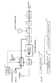
- An arrangement of such a transmission device is shown in
Fig. 10 . In this transmission device, when having received data X (I, Q) of a base band as an input, adistortion compensator 1 multiplies to the input data a distortion compensating coefficient of anRF power amp 6. An output signal of thedistortion compensator 1 applied with the distortion compensating coefficient is converted by a D/A converter 2 into an analog IQ signal to be provided to amodulator 3. Thismodulator 3 performs a direct modulation with alocal oscillator 4 of a carrier frequency (for example, 2.1 GHz bandwidth) to generate an RF signal. - The RF signal thus generated passes through a coupler 5 that forms an input signal detector of an
RF power amp 6 and inputted to theamp 6. A signal power-amplified by theRF power amp 6 passes through acoupler 7 that forms an output signal detector of theRF power amp 6 together with acoupler 13 and transmitted to anantenna 8. It is to be noted that thecouplers 5 and 7 respectively branch their input signals to an ampinput monitor terminal 11a and an amp output monitor terminal 11b, and that a source of theRF power amp 6 is switched ON or OFF by apower amp switch 10. - For updating the distortion compensating coefficient of the
distortion compensator 1, thecoupler 13 provides a branched signal from its input signal to afrequency converter 15, which downconverts its input signal into an intermediate frequency (IF) signal with alocal oscillator 16. The output signal of thefrequency converter 15 is converted into a digital signal by an A/D converter 17 and provided to thedistortion compensator 1, forming a feedback route. Thedistortion compensator 1 compares the input data X (I, Q) with the feedback data from the A/D converter 17 to update the distortion compensating coefficient, thereby suppressing distortion components of theRF power amp 6. - When a switching signal KS from the
power amp switch 10 is made OFF or reset, the source within theRF power amp 6 is powered down so that its transmission output is suspended. For example, when experiments are desired to be performed while suspending the transmission output of thepower amp 6, thepower amp switch 10 is made OFF, whereby in the absence of a transmission wave from theantenna 8, such an event that theRF power amp 6 is faulted due to a reflecting wave does not occur even though the output of theantenna 8 is not terminated. - The amp
input monitor terminal 11a outputs the input signal of theRF power amp 6 which is branched at the coupler 5, which is used in such a case where the transmission wave is required to be confirmed at the above experiments. Even at the suppression of theRF power amp 6, a signal comes in up to the input terminal of theRF power amp 6, so that the transmission wave can be recognized by monitoring the signal. - The amp output monitor terminal 11b provides the output signal of the
RF power amp 6 coupled by e.g. several 10 dB at thecoupler 7. This enables the transmission output waveform to be recognized at the output terminal of theRF power amp 6 even upon theantenna 8 being connected, and also the transmission output level to be recognized if a coupling quantity of thecoupler 7 is prescribed. It is of course that the transmission waveform can not be observed when thepower amp switch 10 is made OFF. - As a reference document, there has been proposed a plural-mode shared transmitting circuit comprising local oscillation circuits, quadrature modulating circuits, gain variable circuits, power amp circuits and output monitor circuits respectively provided for each mode, in which a switch which selects monitor signals outputted from the output monitor circuits of the respective modes and inputs them into an output wave detecting circuit is as to enable sharing the output wave detecting circuit and a difference detecting circuit by the plural modes and the switch which selects differential voltage outputted from the difference detecting circuit and inputs them into gain variable circuits are provided; thus, an automatic power control circuit is shared so that the circuit scale and volume are reduced and the cost is also reduced (See e.g. Patent document 1).
[ Patent document 1 ] Japanese Patent Application Laid-open No.9-312578 - While downsizing the radio base station is a big issue for recent customers' demands, the above arrangement is disadvantageous in that it has two monitor terminals, i.e. an amp input monitor terminal and an amp output monitor terminal, causing the surface area of the device to be enlarged.
- The above arrangement uses the amp input monitor terminal at the time when the source of the power amp is turned or switched OFF, while using the amp output monitor terminal at the time when the source of the power amp is switched ON. Therefore, each time the power amp is switched ON or OFF, the connections of the monitor terminals have to be changed, resulting in a poor operability.
- As shown in
Fig.11 , a predistortion type distortion compensation is a technology for decreasing distortions at the output terminal of the power amp by predicting a distortion quantity f(p) based on a non-linear characteristic of the power amp and applying a signal preliminarily multiplied with a reverse distortion characteristic h(p) of the power amp to the input signal x(p) (step S100) (step S200). Resultantly, at the amp input monitor terminal, a signal h(p) * x(p) applied with the reverse distortion characteristic h(p) of the power amp is to be observed. -
JP 2001 148838 - It is accordingly desirable to provide a transmission device comprising an RF power amp, in which the number of terminals for monitoring the input/output of the power amp is reduced.
- It is also desirable to provide a transmission device comprising an RF power amp, in which distortion components of an input monitor wave of the power amp when the power amp is switched OFF are decreased.
- According to an aspect of the invention, there is provided a transmission device comprising: an RF power amplifier; an input signal detector configured to detect an input signal of the power amplifier; an output signal detector configured to detect an output signal of the power amplifier; a first power amp switch configured to switch ON or OFF the power amplifier; a monitor terminal; and an RF switch configured to select the input signal or the output signal of the power amp to be transmitted to the monitor terminal, in association with the first power amp switch being switched ON or OFF.
- Namely, according to an aspect of the present invention, for the solution of (1) problem on mounting and (2) problem on operability as aforementioned, the amp input monitor terminal and the amp output monitor terminal are unified as a single terminal to selectively monitor the amp input waveform or the amp output waveform in association with the power amp switch being made ON or OFF.
- Therefore, with the ON/OFF signal of the power amp switch being made a control signal of the RF switch, the output signal of the power amp is selected when the power amp switch is, for example, made ON, while the input signal of the power amp is selected when the power amp switch is made OFF, to be provided as an output from the monitor terminal.
- This enables the number of the monitor terminal to be confined to one and at the same time the monitor terminal is not required to be changed depending on ON/OFF state of the power amp, so that downsizing the RF base station and improving operability can be realized.
- It is to be noted that in a front stage of the above input signal detector, a series circuit comprising a distortion compensator, a D/A converter, and a modulator may be connected, and that a coupler may be used for the above detectors.
In one embodiment, the transmission device further comprises a distortion compensator provided in a front stage of the input signal detector, a feedback route connected to the distortion compensator, and a second RF switch configured to select the input signal or the output signal of the power amp to be transmitted to the distortion compensator through the feedback route, in association with the power amp switch being switched ON or OFF. - Namely, with regard to (3) problem on distortion compensation as aforementioned, when the power amp is in OFF state, a feedback signal necessary for the distortion compensation is applied to the input side of the power amp in a feedback distortion compensating mode, whereby distortion components of input waves of the power amp to be monitored at the monitor terminal can be suppressed. When the power amp is in ON state, the output signal of the power amp obtained by performing the distortion compensation is monitored at the monitor terminal.
- It is to be noted that in a front stage of the above input signal detector, the distortion compensator, the D/A converter, and the modulator may be serially connected, in which each of the above detectors may be composed of two couplers one of which branches its input signal to each RF switch.
- In one embodiment, the transmission device further comprises a distortion compensator provided in a front stage of the power amp, a feedback route feeding back the output signal of the power amp to the distortion compensator, and a selector configured to validate or invalidate the distortion compensator, in association with the power amp switch being switched ON or OFF.
- Also in this case, with regard to (3) problem on distortion compensation as aforementioned, when the power amp is in OFF state where distortion components up to the input terminal of the power amp are originally quite small, a transmission signal with less distortion components can be monitored at the monitor terminal by suspending the distortion compensating function to output the modulated transmission wave X (I, Q) as it is. Also, when the power amp is in ON state, the output signal of the power amp subject to the distortion compensation is monitored at the monitor terminal in the same manner as the above by again validating the distortion compensating function.
- In one embodiment, the transmission device further comprise a series circuit including a distortion compensator, a D/A converter, and a modulator connected in a front stage of the input signal detector, wherein the input signal detector comprises a single coupler, the output signal detector comprises two couplers configured to branch the input signals to the RF switch and the feedback route, and the selector comprises a selector configured to make the distortion compensator connect to the D/A converter or bypassed, in association with the power amp switch being switched ON or OFF.
- In one embodiment, the feedback route comprises a frequency converter and an A/D converter connected between the couplers of the output signal detector and the distortion compensator.
- According to an aspect of the present invention, it is made possible to decrease the number of a monitor terminal of an RF power amp, and to monitor waveforms with less distortion components not only at the output but also the input of the power amp, depending on the power amp being made ON or OFF.
- The above and other advantages of the invention will be apparent upon consideration of the following detailed description, taken in conjunction with the accompanying drawings, in which the reference numerals refer to like parts throughout and in which:
-
Fig.1 is a block diagram showing an embodiment [1] of a transmission device; -
Fig.2 is a block diagram for illustrating an operation at an RF switch being made ON, in an embodiment [1] of a transmission device ; -
Fig.3 is a block diagram for illustrating an operation at an RF switch being made OFF, in an embodiment [1] of a transmission device ; -
Fig.4 is a block diagram showing an embodiment [2] of a transmission device; -
Fig.5 is a block diagram for illustrating an operation at an RF switch being made ON, in an embodiment [2] of a transmission device ; -
Fig.6 is a block diagram for illustrating an operation at an RF switch being made OFF, in an embodiment [2] of a transmission device; -
Fig.7 is a block diagram showing an embodiment [3] of a transmission device; -
Fig.8 is a block diagram for illustrating an operation at an RF switch being made ON, in an embodiment [3] of a transmission device; -
Fig.9 is a block diagram for illustrating an operation at an RF switch being made OFF, in an embodiment [3] of a transmission device; -
Fig.10 is a block diagram showing a transmission device; and -
Fig.11 is a block diagram for illustrating a predistortion type distortion compensating operation. -
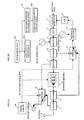
Fig.1 shows an embodiment [1] of a transmission device, in which anRF switch 9 is added to the prior art transmission device shown inFig.10 . Namely, the input signal of the coupler 5 and the input signal of thecoupler 7 are respectively branched and provided to theRF switch 9; the switching signal KS from thepower amp switch 10 is provided to theRF power amp 6 as well as theRF switch 9; the output signal of theRF switch 9 is provided to asingle monitor terminal 11. In this embodiment [1], a feedback route to thedistortion compensator 1 is not connected. -
Figs.2 and3 illustrate specific operations, in the arrangement ofFig.1 , where a monitoring signal for theRF power amp 6 is selected by thepower amp switch 10. - Referring to an operation example at the time when the switching signal KS from the
power amp switch 10 is made ON as shown inFig.2A , input data X (I, Q) from a base band portion (not shown) are multiplied with a distortion compensating coefficient by thedistortion compensator 1, converted into an analog signal by the D/A converter 2, modulated by themodulator 3, passed through the coupler 5, and is provided to theRF power amp 6 for monitoring the input wave thereof. The output signal of theRF power amp 6 passes through thecoupler 7 and is transmitted from theantenna 8. - At this time, the output signal (switching signal) KS of the
power amp switch 10 indicates ON state (step S1 inFig.2B ), making the source of theRF power amp 6 ON (step S2) and switching theRF switch 9 over to the connection of a thick line shown. - As a result, the
RF switch 9 selects the signal branched from thecoupler 7 or the output signal of thepower amp 6 within the signals branched from the couplers 5 and 7 (step S3), to be transmitted from theantenna 8. -
Fig.3A illustrates an operation at the time when the switching signal KS from thepower amp switch 10 is made OFF. In the presence of the OFF signal from the power amp switch 10 (step S11 inFig.3A ), the source of theRF power amp 6 is made OFF (step S12) while at the same time the output of theRF switch 9 is switched over to the input side of the RF power amp 6 (step S13). At this time, no transmission signal is provided to theantenna 8, so that even though theantenna 8 is opened (even in the state of total reflection) theRF power amp 6 will not fail or excessive heat generation will not occur. -
Fig.4 shows an embodiment [2] of a transmission device, which is different from the above embodiment [1] in that there is provided a feedback route to thedistortion compensator 1 to reduce distortion components of the output of thepower amp 6. Namely, as with the prior art shown inFig.10 , a signal branched from thecoupler 13 is fedback to thedistortion compensator 1 via thefrequency converter 15 and the A/D converter 17, and besides there is provided anotherRF switch 14, between thecoupler 13 and thefrequency converter 15 under control of the switching signal KS concurrently with thepower amp 6 and theRF switch 9. To this RF switch 14 a signal branched from acoupler 12 connected between themodulator 3 and the coupler 5 is provided in addition to the signal branched from thecoupler 13, and the output of theRF switch 14 is provided to thefrequency converter 15. -
Figs.5 and6 illustrate specific operations, where the monitoring output of theRF power amp 6 is variously switched over in association with thepower amp switch 10. - Referring to an operation example at the time when the switching signal KS from the
power amp switch 10 is made ON as shown inFig.5A , the input data X (I, Q) is multiplied with a distortion compensating coefficient by thedistortion compensator 1, converted into an analog signal by the D/A converter 2, and then modulated by themodulator 3, forming an input signal of theRF power amp 6. This input signal is obtained after having passed through thecoupler 12 for feedback and the coupler 5 for monitor, both of which form an input signal detector. An output wave amplified by theRF power amp 6 passes through thecoupler 13 for feedback and thecoupler 7 for monitor, both of which form an output signal detector, and is transmitted from theantenna 8. - When the switching signal KS from the
power amp switch 10 is made ON (step S31 inFig.5B ), the source of theRF power amp 6 is powered on (step S32), at which time theRF switch 14 which forms a feedback route switching portion is switched over to the amp output side (step S33) to perform distortion compensating operations. Namely, since the feedback route is connected from the output side of theRF power amp 6, an output waveform with less distortion can be obtained from the antenna 8 (step S34). -
Fig.6A shows a state where the switching signal KS from thepower amp switch 10 is made OFF (step S41 inFig.6B ). When the switching signal KS is made OFF, the source of theRF power amp 6 is made OFF (step S42), at which time theRF switch 14 as a feedback route switching portion selects the branched signal of thecoupler 12 on the input side of the RF power amp 6 (step S43) to perform distortion compensating operations. Namely, since the feedback route is connected on the input side of theRF power amp 6, waveforms in which distortion components which can exist on the input side of thepower amp 6 are compensated by thedistortion compensator 1 can be obtained from themonitor terminal 11. -
Fig.7 shows an embodiment [3] of a transmission device. This embodiment [3] is different from the above embodiment [1] in that for outputting a modulated wave as it is with the distortion compensating function being suspended, the same feedback route as the prior art shown inFig. 10 is provided, and aselector 18 is provided for validating/invalidating thedistortion compensator 1 controlled by the feedback route in association with the switching signal KS from thepower amp switch 10 being made ON or OFF. Therefore, this embodiment [3] only has to use a single coupler as an input signal detector. -
Figs.8 and9 illustrate specific operations where the monitoring output of theRF power amp 6 is variously switched over in association with thepower amp switch 10. - In an operation example where the switching signal KS from the
power amp switch 10 is made ON as shown inFig.8A (step S61 inFig.8B ), theRF power amp 6 is made ON (step S62), and theselector 18 selects thedistortion compensator 1 as shown by a thick line (step S63) to perform the distortion compensation with the input data X (I, Q) multiplied with a distortion compensating coefficient (step S64). At this time, the feedback route is connected from the output side of theRF power amp 6, so that an output waveform with less distortion can be obtained from theantenna 8. - It is to be noted that the
RF switch 9 at this time transmits the branched signal from thecoupler 7, that is an output signal of theRF power amp 6 to themonitor terminal 11 as with the aboveFigs.2 and5 . -
Fig.9A shows a state where the switching signal KS from thepower amp switch 10 is made OFF. When thepower amp switch 10 is powered down (step S71 inFig.9B ), the source of theRF power amp 6 is made OFF (step S72) and concurrently theRF switch 9 selects the branched signal of the coupler 5, that is an input signal of theRF power amp 6, to be provided to themonitor terminal 11. At this time, a through input at theselector 18 is made active (step S73), so that thedistortion compensator 1 is bypassed to invalidate the distortion compensating operation (step S74). - At this time, a route without the multiplication of the distortion compensating coefficient by the
distortion compensator 1 is selected or no distortion compensation is applied, where distortion components arising on the input side of theRF power amp 6 are inherently little, so that distortions become less than the waveform in the application of the distortion compensating coefficient for thepower amp 6, enabling waveforms with less distortions (wave only applied with modulation) to be monitored at themonitor terminal 11. - It is to be noted that the present invention is not limited by the above-mentioned embodiments, and it is obvious that various modifications may be made by one skilled in the art based on the recitation of the claims.
Claims (8)
- A transmission device comprising:an RF power amplifier (6);an input signal detector (5) configured to detect an input signal of the power amplifier;an output signal detector (7) configured to detect an output signal of the power amplifier;a first power amplifier switch (10) configured to switch ON or OFF the power amplifier;a monitor terminal (11); andan RF switch (9) configured to select the input signal or the output signal of the power amplifier to be transmitted to the monitor terminal, in association with the first power amplifier switch being switched ON or OFF.
- The transmission device as claimed in claim 1, further comprising a distortion compensator (1) provided in a front stage of the input signal detector, a feedback route connected to the distortion compensator, and a second RF switch (14) configured to select the input signal or the output signal of the power amplifier to be transmitted to the distortion compensator through the feedback route, in association with the power amplifier switch being switched ON or OFF.
- The transmission device as claimed in claim 1, further comprising a distortion compensator (1) provided in a front stage of the power amplifier, a feedback route feeding back the output signal of the power amplifier to the distortion compensator, and a selector (18) configured to validate or invalidate the distortion compensator, in association with the power amplifier switch being switched ON or OFF.
- The transmission device as claimed in claim 1, further comprising a series circuit including a distortion compensator (1), a D/A converter (2), and a modulator (3) connected in a front stage of the input signal detector.
- The transmission device as claimed in claim 1, further comprising a series circuit including a distortion compensator (1), a D/A converter (2), and a modulator (3) connected in a front stage of the input signal detector, wherein each detector comprises two couplers (5, 7, 12, 13) configured to branch the input signals to each RF switch.
- The transmission device as claimed in claim 2, wherein the feedback route includes a frequency converter (15) and an A/D converter (17) connected between the second RF switch and the distortion compensator.
- The transmission device as claimed in claim 3, further comprising a series circuit including a distortion compensator (1), a D/A converter (2), and a modulator (3) connected in a front stage of the input signal detector, wherein the input signal detector comprises a single coupler (5), the output signal detector comprises two couplers (7, 13) configured to branch the input signals to the RF switch and the feedback route, and the selector comprises a selector configured to make the distortion compensator connect to the D/A converter or bypassed, in association with the power amplifier switch being switched ON or OFF.
- The transmission device as claimed in claim 7, wherein the feedback route comprises a frequency converter (15) and an A/D converter (17) connected between the couplers of the output signal detector and the distortion compensator.
Applications Claiming Priority (1)
| Application Number | Priority Date | Filing Date | Title |
|---|---|---|---|
| JP2007147205A JP4757231B2 (en) | 2007-06-01 | 2007-06-01 | Transmitter |
Publications (3)
| Publication Number | Publication Date |
|---|---|
| EP1998456A2 EP1998456A2 (en) | 2008-12-03 |
| EP1998456A3 EP1998456A3 (en) | 2014-12-03 |
| EP1998456B1 true EP1998456B1 (en) | 2015-09-02 |
Family
ID=39714132
Family Applications (1)
| Application Number | Title | Priority Date | Filing Date |
|---|---|---|---|
| EP08156951.9A Expired - Fee Related EP1998456B1 (en) | 2007-06-01 | 2008-05-27 | Transmission device |
Country Status (4)
| Country | Link |
|---|---|
| US (1) | US7962107B2 (en) |
| EP (1) | EP1998456B1 (en) |
| JP (1) | JP4757231B2 (en) |
| CN (1) | CN101316107B (en) |
Families Citing this family (2)
| Publication number | Priority date | Publication date | Assignee | Title |
|---|---|---|---|---|
| JP6707883B2 (en) * | 2016-02-05 | 2020-06-10 | 沖電気工業株式会社 | Transmitter and distortion compensation method |
| CN114448884B (en) * | 2022-03-02 | 2023-10-20 | 深圳市友华通信技术有限公司 | Routing equipment, power calibration method of routing equipment and storage medium |
Family Cites Families (15)
| Publication number | Priority date | Publication date | Assignee | Title |
|---|---|---|---|---|
| JPH0413444Y2 (en) * | 1989-07-05 | 1992-03-30 | ||
| JP3813247B2 (en) | 1996-05-22 | 2006-08-23 | 松下電器産業株式会社 | Multiple mode shared transmission circuit |
| JP3611690B2 (en) * | 1996-10-14 | 2005-01-19 | 沖電気工業株式会社 | Semiconductor device |
| US6525605B2 (en) * | 1998-08-19 | 2003-02-25 | Harris Corporation | Power amplifier system having frequency and amplifier failure compensation |
| JP3274670B2 (en) * | 1999-11-19 | 2002-04-15 | エヌイーシーケーブルメディア株式会社 | Bidirectional signal monitor circuit |
| JP2002009556A (en) * | 2000-06-16 | 2002-01-11 | Sony Corp | Device and method for compensating distortion |
| JP2002314345A (en) * | 2001-04-16 | 2002-10-25 | Sony Corp | High frequency amplifier circuit and radio communication equipment using the same |
| JP2005159672A (en) * | 2003-11-25 | 2005-06-16 | Yagi Antenna Co Ltd | Broadband amplifier apparatus |
| US7151405B2 (en) * | 2004-07-14 | 2006-12-19 | Raytheon Company | Estimating power amplifier non-linearity in accordance with memory depth |
| US7602155B2 (en) * | 2005-07-27 | 2009-10-13 | Artesyn Technologies, Inc. | Power supply providing ultrafast modulation of output voltage |
| US7761065B2 (en) * | 2006-02-03 | 2010-07-20 | Quantance, Inc. | RF power amplifier controller circuit with compensation for output impedance mismatch |
| US7509102B2 (en) * | 2006-04-07 | 2009-03-24 | Broadcom Corporation | DAC based switching power amplifier |
| US7558542B2 (en) * | 2006-06-09 | 2009-07-07 | Mediatek Inc. | System and method for providing a transmitter for polar modulation and power amplifier linearization |
| US7881401B2 (en) * | 2006-11-17 | 2011-02-01 | Infineon Technologies Ag | Transmitter arrangement and signal processing method |
| US7787564B1 (en) * | 2007-03-13 | 2010-08-31 | Kiomars Anvari | Combined peak reduction equalizer and phase/amplitude pre-distortion |
-
2007
- 2007-06-01 JP JP2007147205A patent/JP4757231B2/en active Active
-
2008
- 2008-05-27 EP EP08156951.9A patent/EP1998456B1/en not_active Expired - Fee Related
- 2008-05-30 US US12/130,639 patent/US7962107B2/en active Active
- 2008-05-30 CN CN2008101081706A patent/CN101316107B/en not_active Expired - Fee Related
Also Published As
| Publication number | Publication date |
|---|---|
| JP4757231B2 (en) | 2011-08-24 |
| US7962107B2 (en) | 2011-06-14 |
| US20080299920A1 (en) | 2008-12-04 |
| CN101316107B (en) | 2012-08-22 |
| CN101316107A (en) | 2008-12-03 |
| JP2008301365A (en) | 2008-12-11 |
| EP1998456A2 (en) | 2008-12-03 |
| EP1998456A3 (en) | 2014-12-03 |
Similar Documents
| Publication | Publication Date | Title |
|---|---|---|
| US7489910B2 (en) | Wireless transmitter and amplifier | |
| KR100844398B1 (en) | Multi-level power amplifier | |
| US20040183593A1 (en) | Power amplification apparatus of portable terminal | |
| WO2009045686A2 (en) | Inverted doherty amplifier with increased off-state impedence | |
| US9837966B1 (en) | Series-type Doherty amplifier | |
| US9148100B2 (en) | Parallel amplifier architecture with feedback control based on reflected signal strength | |
| WO2013015778A1 (en) | Actively tuned circuit having parallel carrier and peaking paths | |
| EP0844732B1 (en) | Linearizer bridge circuit | |
| JPH09232992A (en) | Rf duplexer bypass method for transceiver | |
| EP1998456B1 (en) | Transmission device | |
| US7254377B2 (en) | Parallel operation system of transmission amplifier | |
| US6326841B1 (en) | Method and apparatus for compensating for loss or RF output power from the isolation port of a hybrid coupler | |
| JP2010028799A (en) | Receiving system | |
| US6218897B1 (en) | Reconfigurable linear power amplifier | |
| KR100309720B1 (en) | Feed-forward linear power amplifier with amplifier for compensating delay | |
| KR101131910B1 (en) | Output power unit for a mobile telecommunication equipments | |
| KR100983517B1 (en) | Power amplifier for improving output signal in eebts | |
| KR100371531B1 (en) | Feedforward linear power amplifier using error feedback | |
| JP2001196870A (en) | Power amplifier | |
| EP0784379B1 (en) | Nonlinear compensating circuit | |
| US8670675B2 (en) | System and method for distortion compensation including configureable delay | |
| Singh et al. | PA Output Power and Efficiency Enhancement Across the 2: 1 VSWR Circle using Static Active Load Adjustment | |
| EP1124334A1 (en) | Radio station for transmitting and receiving radio signals | |
| JPH09312578A (en) | Plural-mode shared transmitting circuit | |
| GB2437573A (en) | Combiner circuit for Doherty amplifier |
Legal Events
| Date | Code | Title | Description |
|---|---|---|---|
| PUAI | Public reference made under article 153(3) epc to a published international application that has entered the european phase |
Free format text: ORIGINAL CODE: 0009012 |
|
| AK | Designated contracting states |
Kind code of ref document: A2 Designated state(s): AT BE BG CH CY CZ DE DK EE ES FI FR GB GR HR HU IE IS IT LI LT LU LV MC MT NL NO PL PT RO SE SI SK TR |
|
| AX | Request for extension of the european patent |
Extension state: AL BA MK RS |
|
| PUAL | Search report despatched |
Free format text: ORIGINAL CODE: 0009013 |
|
| AK | Designated contracting states |
Kind code of ref document: A3 Designated state(s): AT BE BG CH CY CZ DE DK EE ES FI FR GB GR HR HU IE IS IT LI LT LU LV MC MT NL NO PL PT RO SE SI SK TR |
|
| AX | Request for extension of the european patent |
Extension state: AL BA MK RS |
|
| RIC1 | Information provided on ipc code assigned before grant |
Ipc: H03F 1/32 20060101ALI20141030BHEP Ipc: H03F 3/72 20060101ALI20141030BHEP Ipc: H04B 1/04 20060101AFI20141030BHEP |
|
| 17P | Request for examination filed |
Effective date: 20141217 |
|
| RBV | Designated contracting states (corrected) |
Designated state(s): AT BE BG CH CY CZ DE DK EE ES FI FR GB GR HR HU IE IS IT LI LT LU LV MC MT NL NO PL PT RO SE SI SK TR |
|
| GRAP | Despatch of communication of intention to grant a patent |
Free format text: ORIGINAL CODE: EPIDOSNIGR1 |
|
| INTG | Intention to grant announced |
Effective date: 20150325 |
|
| RAP1 | Party data changed (applicant data changed or rights of an application transferred) |
Owner name: FUJITSU LIMITED |
|
| RIN1 | Information on inventor provided before grant (corrected) |
Inventor name: NOHIRA, TOMOYOSHI Inventor name: SHAKO, HIDEHARU Inventor name: OHBA, TAKESHI |
|
| GRAS | Grant fee paid |
Free format text: ORIGINAL CODE: EPIDOSNIGR3 |
|
| GRAA | (expected) grant |
Free format text: ORIGINAL CODE: 0009210 |
|
| AKX | Designation fees paid |
Designated state(s): DE FR GB |
|
| AK | Designated contracting states |
Kind code of ref document: B1 Designated state(s): DE FR GB |
|
| REG | Reference to a national code |
Ref country code: GB Ref legal event code: FG4D |
|
| REG | Reference to a national code |
Ref country code: DE Ref legal event code: R096 Ref document number: 602008039900 Country of ref document: DE |
|
| REG | Reference to a national code |
Ref country code: FR Ref legal event code: PLFP Year of fee payment: 9 |
|
| REG | Reference to a national code |
Ref country code: DE Ref legal event code: R097 Ref document number: 602008039900 Country of ref document: DE |
|
| PLBE | No opposition filed within time limit |
Free format text: ORIGINAL CODE: 0009261 |
|
| STAA | Information on the status of an ep patent application or granted ep patent |
Free format text: STATUS: NO OPPOSITION FILED WITHIN TIME LIMIT |
|
| 26N | No opposition filed |
Effective date: 20160603 |
|
| REG | Reference to a national code |
Ref country code: FR Ref legal event code: PLFP Year of fee payment: 10 |
|
| REG | Reference to a national code |
Ref country code: FR Ref legal event code: PLFP Year of fee payment: 11 |
|
| PGFP | Annual fee paid to national office [announced via postgrant information from national office to epo] |
Ref country code: GB Payment date: 20180329 Year of fee payment: 11 |
|
| PGFP | Annual fee paid to national office [announced via postgrant information from national office to epo] |
Ref country code: DE Payment date: 20180515 Year of fee payment: 11 |
|
| PGFP | Annual fee paid to national office [announced via postgrant information from national office to epo] |
Ref country code: FR Payment date: 20180412 Year of fee payment: 11 |
|
| REG | Reference to a national code |
Ref country code: DE Ref legal event code: R119 Ref document number: 602008039900 Country of ref document: DE |
|
| GBPC | Gb: european patent ceased through non-payment of renewal fee |
Effective date: 20190527 |
|
| PG25 | Lapsed in a contracting state [announced via postgrant information from national office to epo] |
Ref country code: DE Free format text: LAPSE BECAUSE OF NON-PAYMENT OF DUE FEES Effective date: 20191203 Ref country code: GB Free format text: LAPSE BECAUSE OF NON-PAYMENT OF DUE FEES Effective date: 20190527 |
|
| PG25 | Lapsed in a contracting state [announced via postgrant information from national office to epo] |
Ref country code: FR Free format text: LAPSE BECAUSE OF NON-PAYMENT OF DUE FEES Effective date: 20190531 |