EP1995821B1 - Speisungsvorrichtung, Antennenspeisungssubsystem und Basisstationssystem - Google Patents
Speisungsvorrichtung, Antennenspeisungssubsystem und Basisstationssystem Download PDFInfo
- Publication number
- EP1995821B1 EP1995821B1 EP08009515.1A EP08009515A EP1995821B1 EP 1995821 B1 EP1995821 B1 EP 1995821B1 EP 08009515 A EP08009515 A EP 08009515A EP 1995821 B1 EP1995821 B1 EP 1995821B1
- Authority
- EP
- European Patent Office
- Prior art keywords
- broad
- stage
- multilayered dielectric
- output
- side coupler
- Prior art date
- Legal status (The legal status is an assumption and is not a legal conclusion. Google has not performed a legal analysis and makes no representation as to the accuracy of the status listed.)
- Active
Links
- 230000008878 coupling Effects 0.000 claims description 73
- 238000010168 coupling process Methods 0.000 claims description 73
- 238000005859 coupling reaction Methods 0.000 claims description 73
- 101100520142 Caenorhabditis elegans pin-2 gene Proteins 0.000 description 13
- 101150037009 pin1 gene Proteins 0.000 description 13
- 230000000694 effects Effects 0.000 description 11
- 238000010586 diagram Methods 0.000 description 10
- 101100244014 Neurospora crassa (strain ATCC 24698 / 74-OR23-1A / CBS 708.71 / DSM 1257 / FGSC 987) ppi-5 gene Proteins 0.000 description 8
- 101150023294 PIN4 gene Proteins 0.000 description 8
- 239000010410 layer Substances 0.000 description 8
- 238000012545 processing Methods 0.000 description 8
- 239000000463 material Substances 0.000 description 6
- 238000000034 method Methods 0.000 description 4
- 238000007493 shaping process Methods 0.000 description 4
- 239000011159 matrix material Substances 0.000 description 3
- 238000010295 mobile communication Methods 0.000 description 3
- 238000001228 spectrum Methods 0.000 description 3
- 238000004891 communication Methods 0.000 description 2
- 238000012938 design process Methods 0.000 description 2
- 238000009826 distribution Methods 0.000 description 2
- 230000035945 sensitivity Effects 0.000 description 2
- 230000002411 adverse Effects 0.000 description 1
- 238000013459 approach Methods 0.000 description 1
- 238000013461 design Methods 0.000 description 1
- 238000005562 fading Methods 0.000 description 1
- 238000003780 insertion Methods 0.000 description 1
- 230000037431 insertion Effects 0.000 description 1
- 238000009434 installation Methods 0.000 description 1
- 238000002955 isolation Methods 0.000 description 1
- 238000012423 maintenance Methods 0.000 description 1
- 238000004519 manufacturing process Methods 0.000 description 1
- 239000002184 metal Substances 0.000 description 1
- 150000003071 polychlorinated biphenyls Chemical class 0.000 description 1
- 230000008054 signal transmission Effects 0.000 description 1
- 239000000758 substrate Substances 0.000 description 1
- 239000002344 surface layer Substances 0.000 description 1
- 238000003466 welding Methods 0.000 description 1
Images


Classifications
-
- H—ELECTRICITY
- H01—ELECTRIC ELEMENTS
- H01Q—ANTENNAS, i.e. RADIO AERIALS
- H01Q3/00—Arrangements for changing or varying the orientation or the shape of the directional pattern of the waves radiated from an antenna or antenna system
- H01Q3/26—Arrangements for changing or varying the orientation or the shape of the directional pattern of the waves radiated from an antenna or antenna system varying the relative phase or relative amplitude of energisation between two or more active radiating elements; varying the distribution of energy across a radiating aperture
- H01Q3/30—Arrangements for changing or varying the orientation or the shape of the directional pattern of the waves radiated from an antenna or antenna system varying the relative phase or relative amplitude of energisation between two or more active radiating elements; varying the distribution of energy across a radiating aperture varying the relative phase between the radiating elements of an array
- H01Q3/34—Arrangements for changing or varying the orientation or the shape of the directional pattern of the waves radiated from an antenna or antenna system varying the relative phase or relative amplitude of energisation between two or more active radiating elements; varying the distribution of energy across a radiating aperture varying the relative phase between the radiating elements of an array by electrical means
- H01Q3/40—Arrangements for changing or varying the orientation or the shape of the directional pattern of the waves radiated from an antenna or antenna system varying the relative phase or relative amplitude of energisation between two or more active radiating elements; varying the distribution of energy across a radiating aperture varying the relative phase between the radiating elements of an array by electrical means with phasing matrix
Definitions
- the present invention relates to the field of communications, particularly to a feed network device, an antenna feeder subsystem, and a base station system.
- intelligent antenna technique can be used to produce a spatially directed wave beam according to the difference in signal space characteristic between mobile subscribers, so as to align the main lobe of antenna to the direction of arrival of subscriber signals and align the side lobe to the direction of arrival of interference signals, and thereby attain the purpose of utilizing mobile subscriber signals efficiently and eliminating or suppressing interference signals, improve efficiency of radio spectrum utilization and signal transmission, and utilize limited channel resource as far as possible.
- directional antennas can increase antenna gain in uplink and downlink greatly, reduce transmitted power level, improve Signal-to-Noise Ratio (SNR), and effectively overcome channel fading.
- SNR Signal-to-Noise Ratio
- a feed network device i.e., beam shaping network
- the feed network device is a main component of the antenna feeder subsystem in the base station system in 3G mobile communication system; the antenna feeder subsystem is connected to a duplexer in the base station system, and includes a feed network device, a power divider, and an antenna array, which are connected in sequence.
- a signal beam emitted from the Transmitter (TX) in the base station system is shaped and then transmitted to an antenna array, and a feed is provided to the array antenna unit, so that the antennae produce a plurality of separate spatially directed beams, and thereby afford good orientation to the superimposed electromagnetic wave.
- TX Transmitter
- the subscriber By guiding a radio signal to a specified subscriber direction, the subscriber can transmit and receive a signal in a limited directional area, and therefore the communication coverage and system capacity can be increased greatly, the spectrum utilization can be improved, the emission power in the base station can be reduced, the system cost can be reduced, and the interference between signals and the pollution of the electromagnetic environment can be reduced.
- the Receiver (RX) also employs a plurality of separate antennae, the receiving sensitivity in an expected direction can be enhanced, and the signals in an unexpected direction can be suppressed.
- Butler matrix structure is usually used to implement a feed network device;
- Butler matrix structure is a passive and interchangeable circuit, which includes several couplers and phase shifting components, wherein, the couplers are two-input and two-output passive devices.
- a feed network device that provides equal-amplitude output is implemented with 3dB branch line directional couplers in standard Butler matrix topology structure; the feed network device is mainly composed of four 3dB branch line directional couplers and two 45° phase shifters cascaded on a Printed Circuit Board (PCB).
- a 3dB branch line directional coupler is a coupler that provides equal-amplitude output, and a signal at the input port becomes two output signals with an amplitude equal to half of the amplitude of the input signal after passing through the 3dB branch line directional coupler.
- Fig.2 shows the topological structure of a feed network device implemented with 3dB branch line directional couplers, wherein, the output pin1 of the 3dB branch line directional coupler 201 is connected to the input pin3 of the 3dB branch line directional coupler 202 via the 45° phase shifter 205, the output pin2 of the 3dB branch line directional coupler 201 is directly connected to the input pin4 of the 3dB coupler 204, the 45° phase shifter 206, and the other two 3dB branch line directional couplers are connected in a similar way.
- a part of the signal is output from pin1 at the coupling port into the 45° phase shifter 205, and then is output from the input pin3 of the 3dB branch line directional coupler 202 into the 3dB branch line directional coupler 202, and is output from the pins Output1 and Output3 after passing through the 3dB branch line directional coupler 202, respectively;
- the other part of the signal passed through the 3dB branch line directional coupler 201 is output from the direct connection pin2 of the 3dB branch line directional coupler 201 into pin4 of the 3dB branch line directional coupler 203 directly, and is output from pins Output2 and Output4 after passing through the 3dB branch line directional coupler 203.
- the feed network device can be used to divide equally the signal power input from any input port into four outputs at the output port.
- the inventor found that all feed network devices with equal-amplitude output are implemented with branch line directional couplers in the prior art, a main line and a branch line of a branch line directional coupler are arranged in a surface layer of the PCB respectively, with air as a dielectric at one side and PCB material as a dielectric at the other side; therefore, the dielectric constant at the main line side is different to the dielectric constant at the branch line side, which causes poor electrical performance of the feed network device.
- Reference D1 US20050035825 discloses a class of modular, double-sided, edge-mounted printed circuit (PC) board modules and an associated modular network architecture for constructing stripline signal processing networks including high-power analogy amplifiers and beam forming networks for driving multi-beam antenna systems. It also discloses two stages of couplers, both the couplers in the first stage and the couplers in the second stage output signal have equal amplitude.
- EP0313057A2 discloses a phased array antenna system having an array of radiating elements.
- EP0671776A1 discloses a microwave directional coupler, and its emphasis is the specific structure of the microwave directional coupler, D3 does not disclose the two level stage couplers.
- US20060028295 discloses a broadside 90° microwave coupler which is composed of three metal layers in a homogeneous dielectric media, D4 also does not disclose the two level stage couplers.
- US20050122185 discloses a coupler that includes first and second mutually coupled spirals disposed on opposite sides of a dielectric substrate.
- the present invention provides a feed network device, an antenna feeder subsystem, and a base station system, which can improve the electrical performance of existing feed network devices.
- a feed network device comprising: two first stage couplers, two phase shifters, and two second stage couplers cascaded on a Printed Circuit Board, wherein each first stage couplers and second stage couplers is a multilayered dielectric broad-side coupler, and the difference of phase between an output signal at the coupling port and an output signal at the direct connection port is 90° in each multilayered dielectric broad-side coupler; wherein each multilayered dielectric broad-side coupler in the second stage is a multilayered dielectric broad-side coupler that provides output signals at equal amplitude;
- a antenna feeder subsystem includes a feed network device, a power divider, and an antenna array, which are connected in sequence; characterized in that the feed network device is the feed network device described in the first aspect.
- a base station system includes a duplexer and an antenna feeder subsystem connected to the duplexer, wherein, the antenna feeder subsystem includes a feed network device, a power divider, and an antenna array connected in sequence; characterized in that the feed network device is the feed network device described in the first aspect.
- a feed network device comprising: two first stage couplers, two phase shifters, and two second stage couplers cascaded on a Printed Circuit Board, wherein each first stage couplers and second stage couplers is a multilayered dielectric broad-side coupler, and the difference of phase between an output signal at the coupling port and an output signal at the direct connection port is 90° in each multilayered dielectric broad-side coupler; wherein each multilayered dielectric broad-side coupler in the second stage is a multilayered dielectric broad-side coupler that provides output signals at equal amplitude, wherein an input port of each multilayered dielectric broad-side coupler in the first stage is a signal input port, and the other input port is connected with a matched load resistance; two output ports of each multilayered dielectric broad-side coupler in the second stage are signal output ports, wherein the two phase shifters are 90° phase shifters, the direct connection port of the first multilayered dielectric broad-side coupler in the first stage is connected to an input port of the
- a antenna feeder subsystem includes a feed network device, a power divider, and an antenna array, which are connected in sequence; characterized in that the feed network device is the feed network device described in the second aspect.
- a base station system includes a duplexer and an antenna feeder subsystem connected to the duplexer, wherein, the antenna feeder subsystem includes a feed network device, a power divider, and an antenna array connected in sequence; characterized in that the feed network device is the feed network device described in the second aspect.
- a feed network device to shape an array antenna wave beam which is composed of two stages of multilayered dielectric broad-side couplers and two phase shifters which are cascaded on a PCB, wherein, each stage includes two identical multilayered dielectric broad-side couplers, each of which is arranged in a PCB and PCB material is utilized as the dielectric; therefore, the dielectric constants at the two sides of each multilayered dielectric broad-side coupler are identical to each other, and thereby the overall electrical performance of the feed network device is improved.
- the feed network device provided in an embodiment of the present invention is a main component of an antenna feeder subsystem;
- the antenna feeder subsystem includes a feed network device, a power divider, and an antenna array, which are connected in sequence, wherein, the feed network device is connected between the duplexer and the power divider, and two groups of identical feed network devices can be used in the base station system to shape the main and diversity signals and then feed the shaped signals to the array antenna through the power divider.
- any input signal at the input port can be output at equal amplitude; in case the coupling degree of the two multilayered dielectric broad-side couplers in the first stage is adjusted to change the two multilayered dielectric broad-side couplers in the first stage into a multilayered dielectric broad-side couplers that provide unequal-amplitude output, any input signal can be output at unequal amplitude as required.
- phase of an output signal at a coupling port of a multilayered dielectric broad-side coupler leads the phase of an output signal at a direct connection port by 90°, in conjunction with a 45° or 90° phase shifter, the phases of the signals at the four output ports of the feed network can be different to each other by 45° or 90° in sequence.
- the feed network device provided by the embodiment 1 includes four 3dB multilayered dielectric broad-side couplers (401, 402, 403, and 404) and two 45° phase shifters (405 and 406); two 3dB multilayered dielectric broad-side couplers (401 and 404) form the first stage of 3dB multilayered dielectric broad-side couplers, the other two 3dB multilayered dielectric broad-side couplers (402 and 403) form the second stage of 3dB multilayered dielectric broad-side couplers, and the two 45° phase shifters (405 and 406) are connected between the two stages of 3dB multilayered dielectric broad-side couplers and form a passive interchangeable circuit structure.
- the connection is:
- An input port of the 3dB multilayered dielectric broad-side coupler 401 in the first stage is a Load port, which can be connected with a 50 ⁇ matched load resistance 400; the other port of the 3dB multilayered dielectric broad-side coupler 401 serves as the first input port Input 1; the coupling port pin1 of the 3dB multilayered dielectric broad-side coupler 401 in the first stage is connected to the input pin5 of the 3dB multilayered dielectric broad-side coupler 403 in the second stage via the 45° phase shifter 405; the direct connection port pin2 of the 3dB multilayered dielectric broad-side coupler 401 in the first stage is directly connected to the input pin3 of the 3dB multilayered dielectric broad-side coupler 402 in the second stage;
- the 3dB multilayered dielectric broad-side coupler 404 in the first stage is connected in a similar way as the multilayered dielectric broad-side coupler 401, wherein, an input port serves as the Load port and can be connected with a 50 ⁇ matched load resistance 405, the other port serves as the second input port Input2, the direct connection port is directly connected to the input pin6 of the 3dB multilayered dielectric broad-side coupler 403 in the second stage, and the coupling port is connected to the input pin4 of the 3dB multilayered dielectric broad-side coupler 402 in the second stage via the 45° phase shifter 406;
- the four output ports Output2, Output4, Output1, and Output3 of the two 3dB multilayered dielectric broad-side couplers in the second stage are four signal output ports.
- a signal is output as signals at equal amplitude
- the signal output from the coupling port pin1 passes through the 45° phase shifter into the pin5 of the 3dB multilayered dielectric broad-side coupler 403 in the second stage, and then is output at equal amplitude from the coupling port Output1 and the direct connection port Output3 of the 3dB multilayered dielectric broad-side coupler 403 in the second stage;
- the signal output from the direct connection port pin2 directly enters the pin3 of the 3dB multilayered dielectric broad-side coupler 402 in the second stage, and then is output at equal amplitude from the coupling port Output2 and the direct connection port Output4 of the 3dB multilayered dielectric broad-side coupler 402 in the second stage.
- the input signal is distributed to the four output ports and output at equal amplitude
- the phase of a signal output from the output port Output2 leads the phase of a signal output from the output port Output1 by 45°
- the phase of a signal output from the output port Output3 leads the phase of a signal output from the output port Output2 by 45°
- the phase of a signal output from the output port Output4 leads the phase of a signal output from the output port Output3 by 45°.
- Embodiment 2 this embodiment is not an embodiment of the invention but helpful to understand certain aspects thereof.
- the feed network device provided by the embodiment 2 7a includes four 3dB multilayered dielectric broad-side couplers (501, 502, 503, and 504) and two 45° phase shifters (505 and 506); two 3dB multilayered dielectric broad-side couplers (501 and 504) form the first stage of 3dB multilayered dielectric broad-side couplers, the other two 3dB multilayered dielectric broad-side couplers (502 and 503) form the second stage of 3dB multilayered dielectric broad-side couplers, and the two 45° phase shifters (505 and 506) are connected between the two stages of 3dB multilayered dielectric broad-side couplers and form a passive interchangeable circuit structure.
- the connection is:
- An input port of the 3dB multilayered dielectric broad-side coupler 501 in the first stage is a Load port, which can be connected with a 50 ⁇ matched load resistance 500; the other port of the 3dB multilayered dielectric broad-side coupler 501 serves as the first input port Input1; the coupling port pin1 of the 3dB multilayered dielectric broad-side coupler 501 in the first stage is connected to the input pin3 of the 3dB multilayered dielectric broad-side coupler in the second stage via the 45° phase shifter 505; the direct connection port pin2 of the 3dB multilayered dielectric broad-side coupler 501 in the first stage is directly connected to the input pin5 of the 3dB multilayered dielectric broad-side coupler 503 in the second stage;
- the 3dB multilayered dielectric broad-side coupler 504 in the first stage is connected in the same way as the multilayered dielectric broad-side coupler 501, wherein, an input port serves as a Load port and can be connected with a 50 ⁇ matched load resistance 507, the other port serves as the second input port Input2, the direct connection port is directly connected to the input pin4 of the 3dB multilayered dielectric broad-side coupler 502 in the second stage, and the coupling port is connected to the input pin6 of the 3dB multilayered dielectric broad-side coupler 503 in the second stage via the 45° phase shifter 506;
- the four output ports Output1, Output2, Output3, and Output4 of the two 3dB multilayered dielectric broad-side couplers in the second stage are four signal output ports.
- a signal After being input into the 3dB multilayered dielectric broad-side coupler 501 in the first stage from Input1, a signal is output as signals at equal amplitude, wherein, the signal output from the coupling port pin1 passes through the 45° phase shifter 505 into the pin3 of the 3dB multilayered dielectric broad-side coupler 502 in the second stage, and then is output from Output1 and Output3 at equal amplitude; the signal output from the direct connection port pin2 directly enters the pin5 of the 3dB multilayered dielectric broad-side coupler 503 in the second stage, and then is output from Output2 and Output4 at equal amplitude.
- the input signal is distributed to the four output ports and output at equal amplitude
- the phase of a signal output from the output port Output2 leads the phase of a signal output from the output port Output1 by 45°
- the phase of a signal output from the output port Output3 leads the phase of a signal output from the output port Output2 by 45°
- the phase of a signal output from the output port Output4 leads the phase of a signal output from the output port Output3 by 45°.
- the two multilayered dielectric broad-side couplers in the first stage can be designed as multilayered dielectric broad-side couplers that provide unequal-amplitude output.
- the circuit structure is shown in Fig.6 , wherein, the couplers in the first stage are multilayered dielectric broad-side couplers (601 and 604) that provide unequal-amplitude output, and the couplers in the second stage are two 3dB multilayered dielectric broad-side couplers (602 and 603); the two 45° phase shifters (605 and 606) are cascaded between the two stages of couplers.
- the connection is:
- the multilayered dielectric broad-side coupler 604 that provides unequal-amplitude output in the first stage is connected in a similar way as the multilayered dielectric broad-side coupler 601, wherein, one input port is a Load port and can be connected to a 50 ⁇ matched load resistance 607, the other port serves as the second input port Input2, the coupling port of the multilayered dielectric broad-side coupler 604 that provides unequal-amplitude output in the first stage is connected to the pin4 of the 3dB multilayered dielectric broad-side coupler 602 in the second stage via a 45° phase shifter 606, and the direct connection port of the multilayered dielectric broad-side coupler 604 that provides unequal-amplitude output in the first stage is directly connected to the pin6 of the 3dB multilayered dielectric broad-side coupler 603 in the second stage.
- the four output ports Output2, Output4, Output1, and Output3 of the two 3dB multilayered dielectric broad-side couplers in the second stage are four signal output ports.
- a signal is output as signals X and Y at unequal amplitude;
- the signal X output from the coupling port pin1 enters the pin5 of the 3dB multilayered dielectric broad-side coupler 603 in the second stage via the 45° phase shifter 605, and then is output from the coupling port Output1 and the direct connection port Output3 of the 3dB multilayered dielectric broad-side coupler 603 in the second stage at equal amplitude;
- the signal Y output from the direct connection port pin2 enters the pin3 of the 3dB multilayered dielectric broad-side coupler 602 in the second stage directly, and then is output from Output2 and Output4 at equal amplitude.
- the output signals from Output1 and Output2 are different in amplitude; meanwhile, the amplitude of the output signal from Output1 is equal to the amplitude of the output signal from Output3, and the amplitude of the output signal from Output2 is equal to the amplitude of the output signal from Output4; by adjusting the coupling degree of the multilayered dielectric broad-side coupler 601 that provides unequal-amplitude output in the first stage, the amplitude ratio between the output signals from Output2 and Output1 can be set to an expected value.
- the phase of a signal output from the output port Output2 lags the phase of a signal output from the output port Output1 by 45°
- the phase of a signal output from the output port Output3 lags the phase of a signal output from the output port Output2 by 45°
- the phase of a signal output from the output port Output4 lags the phase of a signal output from output port Output3 by 45°.
- the phase of a signal output from the output port Output2 leads the phase of a signal output from the output port Output1 by 45°
- the phase of a signal output from the output port Output3 leads the phase of a signal output from the output port Output2 by 45°
- the phase of a signal output from the output port Output4 leads the phase of a signal output from the output port Output3 by 45°.
- the two multilayered dielectric broad-side couplers in the first stage can be designed as multilayered dielectric broad-side couplers that provide unequal-amplitude output.
- the circuit structure is shown in Fig.7 , wherein, the couplers in the first stage are multilayered dielectric broad-side couplers (701 and 704) that provide unequal-amplitude output, and the couplers in the second stage are two 3dB multilayered dielectric broad-side couplers (702 and 703); the two 45° phase shifters (705 and 706) are cascaded between the two stages of couplers.
- the connection is:
- An input port of the multilayered dielectric broad-side coupler 701 that provides unequal-amplitude output in the first stage is a Load port, which can be connected with a 50 ⁇ matched load resistance 700; the other port of the multilayered dielectric broad-side coupler 701 serves as the first input port Input1; the coupling port pin1 of the multilayered dielectric broad-side coupler 701 that provides unequal-amplitude output in the first stage is connected to the pin3 of the 3dB multilayered dielectric broad-side coupler 702 in the second stage via the 45° phase shifter 705; the direct connection port pin2 of the multilayered dielectric broad-side coupler 701 that provides unequal-amplitude output in the first stage is directly connected to the pin5 of the 3dB multilayered dielectric broad-side coupler 703 in the second stage;
- the multilayered dielectric broad-side coupler 704 that provides unequal-amplitude output in the first stage is connected in a similar way as the multilayered dielectric broad-side coupler 701, wherein, one input port is a Load port and can be connected to a 50 ⁇ matched load resistance 707, and the other port serves as the second input port Input2.
- the four output ports Output1, Output2, Output3, and Output4 of the two 3dB multilayered dielectric broad-side couplers in the second stage are four signal output ports.
- a signal is output as signals X and Y at unequal amplitude;
- the signal X output from the coupling port pin1 enters the pin3 of the 3dB multilayered dielectric broad-side coupler 702 in the second stage via the 45 deg. phase shifter 705, and then is output from Output1 and Output3 at equal amplitude;
- the signal Y output from the direct connection port pin2 enters the pin5 of the 3dB multilayered dielectric broad-side coupler 703 in the second stage directly, 12 and then is output from Output2 and Output4 at equal amplitude.
- the output signals from Output 1 and Output2 are different in amplitude; meanwhile, the amplitude of the output signal from Output1 is equal to the amplitude of the output signal from Output3, and the amplitude of the output signal from Output2 is equal to the amplitude of the output signal from Output4; by adjusting the coupling degree of the multilayered dielectric broad-side coupler 701, the amplitude ratio between the output signals from Output2 and Output1 can be set to an expected value.
- the phase of a signal output from the output port Output2 lags the phase of a signal output from the output port Output1 by 45°
- the phase of a signal output from the output port Output3 lags the phase of a signal output from the output port Output2 by 45°
- the phase of a signal output from the output port Output4 lags the phase of a signal output from output port Output3 by 45°.
- the phase of a signal output from the output port Output2 leads the phase of a signal output from the output port Outputl by 45°
- the phase of a signal output from the output port Output3 leads the phase of a signal output from the output port Output2 by 45°
- the phase of a signal output from the output port Output4 leads the phase of a signal output from the output port Output3 by 45°.
- Embodiment 5 This embodiment is not an embodiment of the invention but helpful to understand certain aspects thereof.
- Two 90° phase shifters can be used to make that the phase of a signal output from the output port Output1 leads the phase of a signal output from the output port.
- the feed network device includes four 3dB multilayered dielectric broad-side couplers (801, 802, 803, and 804) and two 90° phase shifters (805 and 806), wherein:
- the direct connection port pin1 of the 3dB multilayered dielectric broad-side coupler 801 in the first stage is connected to the pin3 of the 3dB multilayered dielectric broad-side coupler 802 in the second stage via the 90° phase shifter 805, the coupling port pin2 of the 3dB multilayered dielectric broad-side coupler 801 in the first stage is directly connected to the pin5 of the 3dB multilayered dielectric broad-side coupler 803 in the second stage;
- the direct connection port pin7 of the 3dB multilayered dielectric broad-side coupler 804 in the first stage is connected to the pin4 of the 3dB multilayered dielectric broad-side coupler 802 in the second stage via the 90° phase shifter 806, the coupling port pin8 of the 3dB multilayered dielectric broad-side coupler 804 in the first stage is directly connected to the pin6 of the 3dB multilayered dielectric broad-side coupler 803 in the second stage;
- each 3dB multilayered dielectric broad-side coupler in the first stage there is an input port which serves as a Load port and can be connected to a 50 ⁇ matched load resistance; the four output ports Output1, Output2, Output3, and Output4 of the two 3dB multilayered dielectric broad-side couplers in the second stage serve as the output ports of the feed network device in sequence.
- a signal After being input into the 3dB multilayered dielectric broad-side coupler 801 in the first stage from Input1, a signal is output as signals at equal amplitude; the signal output from the direct connection port pin1 enters the pin3 of the 3dB multilayered dielectric broad-side coupler 802 in the second stage via the 90° phase shifter 805, and then is output from Output1 and Output2 at equal amplitude; the signal output from the coupling port pin2 enters the pin5 of the 3dB multilayered dielectric broad-side coupler 803 in the second stage directly, and then is output from Output3 and Output4 at equal amplitude.
- a signal is output as signals at equal amplitude; the signal output from the coupling port pin8 enters the pin6 of the 3dB multilayered dielectric broad-side coupler 803 in the second stage directly and then is output from Output3 and Output4 at equal amplitude; the signal output from the direct connection port pin7 passes through the 90° phase shifter 806 and enters the pin4 of the 3dB multilayered dielectric broad-side coupler 802 in the second stage and then is output from Output 1 and Output2 at equal amplitude.
- the input signal is distributed to the four output ports and output at equal amplitude; by the effect of the 90° phase shifters, and due to the characteristic that the phase of output signal at the coupling port of multilayered dielectric broad-side coupler leads the phase of output signal at the direct connection port by 90°, the phase of a signal output from the output port Output2 lags the phase of a signal output from the output port Output 1 by 90°, the phase of a signal output from the output port Output3 lags the phase of a signal output from the output port Output2 by 90°, and the phase of a signal output from the output port Output4 lags the phase of a signal output from output port Output3 by 90°.
- the phase of a signal output from the output port Output2 leads the phase of a signal output from the output port Output1 by 90°
- the phase of a signal output from the output port Output3 leads the phase of a signal output from the output port Output2 by 90°
- the phase of a signal output from the output port Output4 leads the phase of a signal output from the output port Output3 by 90°.
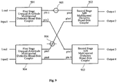
- Fig.9 is a schematic diagram of the topological structure of a feed network device that provides unequal-amplitude output, which is implemented with two 90° phase shifters;
- the multilayered dielectric broad-side couplers in the first stage of the feed network device include two multilayered dielectric broad-side couplers (901 and 904) that provide unequal-amplitude output, and the second stage multilayered dielectric broad-side couplers include two 3dB multilayered dielectric broad-side couplers (902 and 903);
- the two 90° phase shifters (905 and 906) are cascaded between the two stages of multilayered dielectric broad-side couplers.
- a signal is output as two signals at unequal amplitude;
- the signal output from the direct connection port pin1 passes through the 90° phase shifter 905 and enters the pin3 of the 3dB multilayered dielectric broad-side coupler 902 in the second stage, and then is output from Output1 and Output2 at equal amplitude;
- the signal output from the coupling port pin2 enters the pin5 of the 3dB multilayered dielectric broad-side coupler 903 in the second stage directly, and then is output from Output3 and Output4 at equal amplitude.
- a signal is output as two signals at unequal amplitude; the signal output from the coupling port pin8 enters the pin6 of the 3dB multilayered dielectric broad-side coupler 903 in the second stage directly and then is output from Output3 and Output4 with equal amplitude; the signal output from the direct connection port pin7 passes through the 90° phase shifter 906 and enters the pin4 of the 3dB multilayered dielectric broad-side coupler 902 in the second stage and then is output from Output 1 and Output2 at equal amplitude.
- the amplitude of output signal OUT1 is equal to the amplitude of the output signal OUT2
- the amplitude of the output signal OUT3 is equal to the amplitude of the output signal OUT4
- the amplitude ratio between output signals from OUT1 and OUT3 can be set to an expected value.
- the phase of a signal output from the output port Output2 lags the phase of a signal output from the output port Output1 by 90°
- the phase of a signal output from the output port Output3 lags the phase of a signal output from the output port Output2 by 90°
- the phase of a signal output from the output port Output4 lags the phase of a signal output from output port Output3 by 90°.
- the phase of a signal output from the output port Output2 leads the phase of a signal output from the output port Output1 by 90°
- the phase of a signal output from the output port Output3 leads the phase of a signal output from the output port Output2 by 90°
- the phase of a signal output from the output port Output4 leads the phase of a signal output from the output port Output3 by 90°.
- the 45° and 90° phase difference values between the output ports of the feed network device are design values; the actual values may have some error within an allowable range.
- the feed network device described in the embodiments of the present invention is implemented with four layers of boards stacked on a PCB, as shown in Fig.10 . It is seen from the drawing: the top and bottom dielectric layers are a first ground layer 1 and a second ground layer 2, two broad-side coupling lines are arranged on the two intermediate layers respectively and are made of dielectric PCB material, the dielectric is distributed evenly and has the same dielectric constant.
- the two broad-side coupling lines on each multilayered dielectric broad-side coupler are cross distributed in X-shape; that approach can avoid error in coupling degree caused by processing error; wherein, the two input ports are on one side of the multilayered dielectric broad-side coupler, and the two output ports are on the opposite side of the multilayered dielectric broad-side coupler. Therefore, the two signal input ports of the feed network device are distributed on the same side of the PCB, and the four output ports are on the opposite side of the PCB, so as to facilitate installation and maintenance.
- the couplers and phase shifters in the feed network device provided in the present invention can be separate components, which are cascaded via the PCB; the positions of the components can be designed flexibly as required.
- Fig.11 is a top view in direction Z of the two coupled broad-side coupling lines on a multilayered dielectric broad-side coupler. It is seen from Fig. 11 : by setting the length of the coupling lines to a quarter wave length corresponding to the working band, the phase of output signal from the coupling port of the multilayered dielectric broad-side coupler can lead the phase of output signal from the direct connection port by 90°.
- the phase of output signal from the coupling port of the multilayered dielectric broad-side coupler can lead the phase of output signal from the direct connection port by 90°.
- the coupling degree of the multilayered dielectric broad-side couplers in the first stage and the second stage can be adjusted by adjusting the overlapped projection area of the two crossed coupling lines between the second layer and the third layer in direction Z.
- the two broad-side coupling lines are in symmetric structure (e.g., Z-shaped or step-shaped structure) and in X-shaped distribution in space roughly, the overlapped projection area in direction Z will not be changed even if relative deviation (caused by PCB processing error) exists between the two broad-side coupling lines; in that way, error in coupling degree caused by processing error can be avoided.
- the electrical performance parameters of the feed network device are improved; in addition, broad-side coupling further improves the electrical performance parameters of the feed network device, such as high isolation between input and output ports, less insertion loss, and good port standing wave characteristic, etc.; furthermore, the output signal has excellent power flatness and wide bandwidth.
- the size of the feed network device is reduced, and thereby the cost is reduced. Adverse effects of processing error to the coupling degree can be avoided, and the processing uniformity can be assured; both the welding work and the assembling work are easy and quick, and mass production can be carried out.
- the input ports are arranged on a side of the PCB and the output ports are arranged on another side of the PCB, and therefore are easy to install and service.
- corresponding circuits can be designed on PCBs of the same size according to the requirement for equal-amplitude or unequal-amplitude output from the feed network device and the requirement for specific phase difference, so as to improve flexibility of the functionality of the entire feed network device, wherein:
- the first stage of couplers be set as 3dB multilayered dielectric broad-side couplers
- the coupling degree of the two couplers in the first stage be adjusted by means of field emulation.
- the signal wave beam transmitted from the transmitter TX in the base station system enters the feed network device via the duplexer, it can be output at equal amplitude or unequal amplitude, and constant 45° or 90° phase difference exists between the signals output from adjacent output ports (i.e., beam shaping).
- all couplers of the feed network device are multilayered dielectric broad-side couplers arranged in the PCB, with PCB material as the dielectric; therefore, the dielectric is distributed evenly and has the same dielectric constant.
- multilayered dielectric broad-side couplers are used in the feed network device in the embodiments of the present invention and the two broad-side coupling lines of a multilayered dielectric broad-side couplers are in symmetric structure (e.g., Z-shaped or step-shaped structure) and in X-shaped distribution in space roughly, the overlapped projection area of the multilayered broad-side coupling lines on the PCB surface of the feed network device will not be changed even if relative deviation (caused by PCB processing error) exists between the two broad-side coupling lines; in that way, error in coupling degree caused by processing error can be avoided. Therefore, the present invention can improve electrical performance of feed network device, antenna feeder subsystem, and base station system.
- a feed network device When a feed network device provided in the present invention is applied in a base station system in 3G mobile communication system, a input port of the feed network device is connected to a duplexer (a wave beam port), a output port is connected to a input port of a power divider; by shaping a wave beam, the feed network device can provide a plurality of different narrow beams to a antenna array, and thereby system capacity, spectrum utilization ratio, and receiver sensitivity are increased, base station power emission and system cost and reduced, and smooth network expansion is simplified.
- a duplexer a wave beam port
- a output port is connected to a input port of a power divider
- the present invention implements a feed network device that is low in cost, easy to process and assemble, and has good electrical performance and small footprint; in addition, by adjusting the coupling degree of the couplers in the first stage in the design process, the entire feed network device can provide signals output at equal amplitude or unequal amplitude for any input signal, with a constant signal phase difference between the output ports such as 45° or 90°, and thereby perform wave beam shaping flexibly and meet different application demands for the system.
Landscapes
- Waveguide Switches, Polarizers, And Phase Shifters (AREA)
- Variable-Direction Aerials And Aerial Arrays (AREA)
Claims (10)
- Speisungsvorrichtung, umfassend: zwei Erststufenkoppler (601, 604; 701, 704), zwei Phasenschieber (605, 606; 705, 706), und zwei Zweitstufenkoppler (602, 603; 702, 703), die kaskadierend auf einer Leiterplatte angeordnet sind, wobei es sich bei jedem Erststufenkoppler (601, 604; 701, 704) und Zweitstufenkoppler (602, 603; 702, 703) um einen mehrschichtigen dielektrischen Breitseiten-Koppler handelt, und der Phasenunterschied zwischen einem Ausgangssignal an dem Kopplungsport und einem Ausgangssignal an dem Direktverbindungsport in jedem mehrschichtigen dielektrischen Breitseiten-Koppler (601, 602, 603, 604; 701, 702, 703, 704) 90° beträgt;
wobei ein Eingangsport jedes mehrschichtigen dielektrischen Breitseiten-Kopplers in der ersten Stufe (601, 604; 701, 704) ein Signaleingangsport ist, und der andere Eingangsport mit einem angepassten Lastwiderstand verbunden ist; zwei Ausgangsports jedes mehrschichtigen dielektrischen Breitseiten-Kopplers in der zweiten Stufe (602, 603; 702, 703) Signalausgangsports sind,
wobei es sich bei den beiden Phasenschiebern um 45° Phasenschieber handelt, wobei:der Kopplungsport des ersten mehrschichtigen dielektrischen Breitseiten-Kopplers in der ersten Stufe (601; 701) mit einem Eingangsport des ersten mehrschichtigen dielektrischen Breitseiten-Kopplers in der zweiten Stufe (603; 702) über einen 45° Phasenschieber (605; 705) verbunden ist, der Direktverbindungsport des ersten mehrschichtigen dielektrischen Breitseiten-Kopplers in der ersten Stufe (601; 701) direkt mit einem Eingangsport des zweiten mehrschichtigen dielektrischen Breitseiten-Kopplers in der zweiten Stufe (602; 703) verbunden ist;der Kopplungsport des zweiten mehrschichtigen dielektrischen Breitseiten-Kopplers in der ersten Stufe (604; 704) mit dem anderen Eingangsport des zweiten mehrschichtigen dielektrischen Breitseiten-Kopplers in der zweiten Stufe (602; 703) über einen 45° Phasenschieber (606; 706) verbunden ist, und der Direktverbindungsport des zweiten mehrschichtigen dielektrischen Breitseiten-Kopplers in der ersten Stufe (604; 704) direkt mit dem anderen Eingangsport des ersten mehrschichtigen dielektrischen Breitseiten-Kopplers in der zweiten Stufe (603; 702) verbunden ist;wobei die Speisungsvorrichtung dadurch gekennzeichnet ist, dass
jeder mehrschichtige dielektrische Breitseiten-Koppler in der ersten Stufe (601, 604; 701, 704) ein mehrschichtiger dielektrischer Breitseiten-Koppler ist, der Ausgangssignale bei ungleicher Amplitude bereitstellt, und jeder mehrschichtige dielektrische Breitseiten-Koppler in der zweiten Stufe (602, 603; 702, 703) ein mehrschichtiger dielektrischer Breitseiten-Koppler ist, der Ausgangssignale bei gleicher Amplitude bereitstellt. - Speisungsvorrichtung nach Anspruch 1, wobei zwei Breitseiten-Verbindungsleitungen jedes mehrschichtigen dielektrischen Breitseiten-Kopplers kreuzweise verteilt sind, die beiden Eingangsports sich auf einer Seite des mehrschichtigen dielektrischen Breitseiten-Kopplers befinden und die beiden Ausgangsports sich auf der gegenüberliegenden Seite des mehrschichtigen dielektrischen Breitseiten-Kopplers befinden.
- Speisungsvorrichtung nach Anspruch 1, wobei die Leiterplatte vier Schichten umfasst, die zwei Breitseiten-Verbindungsleitungen jedes mehrschichtigen dielektrischen Breitseiten-Kopplers (601, 602, 603, 604; 701, 702, 703, 704) auf zwei Zwischenschichten der Leiterplatte angeordnet sind, die zwei Signaleingangsports der Speisungsvorrichtung auf einer Seite der Leiterplatte angeordnet sind und die vier Signalausgangsports auf der gegenüberliegenden Seite der Leiterplatte angeordnet sind.
- Speisungsvorrichtung, umfassend: zwei Erststufenkoppler (901, 904), zwei Phasenschieber (905, 906) und zwei Zweitstufenkoppler (902, 903), die kaskadierend auf einer Leiterplatte angeordnet sind, wobei es sich bei jedem Erststufenkoppler (901, 904) und Zweitstufenkoppler (902, 903) um einen mehrschichtigen dielektrischen Breitseiten-Koppler handelt, und der Phasenunterschied zwischen einem Ausgangssignal an dem Kopplungsport und einem Ausgangssignal an dem Direktverbindungsport in jedem mehrschichtigen dielektrischen Breitseiten-Koppler (901, 902, 903, 904) 90° beträgt;
wobei ein Eingangsport jedes mehrschichtigen dielektrischen Breitseiten-Kopplers in der ersten Stufe (901, 904) ein Signaleingangsport ist, und der andere Eingangsport mit einem angepassten Lastwiderstand verbunden ist; zwei Ausgangsports jedes mehrschichtigen dielektrischen Breitseiten-Kopplers in der zweiten Stufe (902, 903) Signalausgangsports sind,
wobei es sich bei den zwei Phasenschiebern (905, 906) um 90° Phasenschieber handelt, der Direktverbindungsport des ersten mehrschichtigen dielektrischen Breitseiten-Kopplers (901) in der ersten Stufe mit einem Eingangsport des ersten mehrschichtigen dielektrischen Breitseiten-Kopplers in der zweiten Stufe (902) über einen 90° Phasenschieber (905) verbunden ist und der Kopplungsport des ersten mehrschichtigen dielektrischen Breitseiten-Kopplers in der ersten Stufe (901) direkt mit einem Eingangsport des zweiten mehrschichtigen dielektrischen Breitseiten-Kopplers in der zweiten Stufe (903) verbunden ist;
der Direktverbindungsport des zweiten mehrschichtigen dielektrischen Breitseiten-Kopplers in der ersten Stufe (904) mit dem anderen Eingangsport des ersten mehrschichtigen dielektrischen Breitseiten-Kopplers in der zweiten Stufe (902) über einen 90° Phasenschieber (906) verbunden ist und der Kopplungsport des zweiten mehrschichtigen dielektrischen Breitseiten-Kopplers in der ersten Stufe (904) direkt mit dem anderen Eingangsport des zweiten mehrschichtigen dielektrischen Breitseiten-Kopplers in der zweiten Stufe (903) verbunden ist;
wobei die Speisungsvorrichtung dadurch gekennzeichnet ist, dass:jeder mehrschichtige dielektrische Breitseiten-Koppler in der ersten Stufe (901, 904) ein mehrschichtiger dielektrischer Breitseiten-Koppler ist, der Ausgangssignale bei ungleicher Amplitude bereitstellt, und jeder mehrschichtige dielektrische Breitseiten-Koppler in der zweiten Stufe (902, 903) ein mehrschichtiger dielektrischer Breitseiten-Koppler ist, der Ausgangssignale bei gleicher Amplitude bereitstellt. - Speisungsvorrichtung nach Anspruch 4, wobei zwei Breitseiten-Verbindungsleitungen jedes mehrschichtigen dielektrischen Breitseiten-Kopplers kreuzweise verteilt sind, die beiden Eingangsports sich auf einer Seite des mehrschichtigen dielektrischen Breitseiten-Kopplers befinden und die beiden Ausgangsports sich auf der gegenüberliegenden Seite des mehrschichtigen dielektrischen Breitseiten-Kopplers befinden.
- Speisungsvorrichtung nach Anspruch 4, wobei die Leiterplatte vier Schichten umfasst, die zwei Breitseiten-Verbindungsleitungen jedes mehrschichtigen dielektrischen Breitseiten-Kopplers (901, 902, 903, 904) auf zwei Zwischenschichten der Leiterplatte angeordnet sind, die zwei Signaleingangsports der Speisungsvorrichtung auf einer Seite der Leiterplatte angeordnet sind und die vier Signalausgangsports auf der gegenüberliegenden Seite der Leiterplatte angeordnet sind.
- Antennen-Speiseuntersystem, umfassend eine Speisungsvorrichtung, einen Leistungsteiler und eine in Reihe geschaltete Antennenanordnung, dadurch gekennzeichnet, dass die Speisungsvorrichtung eine Speisungsvorrichtung nach einem der vorhergehenden Ansprüche 1 bis 3 ist.
- Antennen-Speiseuntersystem, umfassend eine Speisungsvorrichtung, einen Leistungsteiler und eine in Reihe geschaltete Antennenanordnung, dadurch gekennzeichnet, dass die Speisungsvorrichtung eine Speisungsvorrichtung nach einem der vorhergehenden Ansprüche 4 bis 6 ist.
- Basisstationssystem, umfassend einen Duplexer und ein Antennen-Speiseuntersystem, das mit dem Duplexer verbunden ist, wobei das Antennen-Speiseuntersystem eine Speisungsvorrichtung, einen Leistungsteiler und eine in Reihe geschaltete Antennenanordnung umfasst, dadurch gekennzeichnet, dass die Speisungsvorrichtung eine Speisungsvorrichtung nach einem der vorhergehenden Ansprüche 1 bis 3 ist.
- Basisstationssystem, umfassend einen Duplexer und ein Antennen-Speiseuntersystem, das mit dem Duplexer verbunden ist, wobei das Antennen-Speiseuntersystem eine Speisungsvorrichtung, einen Leistungsteiler und eine in Reihe geschaltete Antennenanordnung umfasst, dadurch gekennzeichnet, dass die Speisungsvorrichtung eine Speisungsvorrichtung nach einem der vorhergehenden Ansprüche 4 bis 6 ist.
Applications Claiming Priority (2)
| Application Number | Priority Date | Filing Date | Title |
|---|---|---|---|
| CN2007101076794A CN101051860B (zh) | 2007-05-24 | 2007-05-24 | 一种馈电网络装置、天馈子系统和基站系统 |
| PCT/CN2008/070793 WO2008145037A1 (fr) | 2007-05-24 | 2008-04-24 | Dispositif de réseau d'alimentation, sous-système d'alimentation aérien et système de stations de base |
Publications (2)
| Publication Number | Publication Date |
|---|---|
| EP1995821A1 EP1995821A1 (de) | 2008-11-26 |
| EP1995821B1 true EP1995821B1 (de) | 2017-02-22 |
Family
ID=39711972
Family Applications (1)
| Application Number | Title | Priority Date | Filing Date |
|---|---|---|---|
| EP08009515.1A Active EP1995821B1 (de) | 2007-05-24 | 2008-05-23 | Speisungsvorrichtung, Antennenspeisungssubsystem und Basisstationssystem |
Country Status (2)
| Country | Link |
|---|---|
| US (1) | US7839235B2 (de) |
| EP (1) | EP1995821B1 (de) |
Families Citing this family (9)
| Publication number | Priority date | Publication date | Assignee | Title |
|---|---|---|---|---|
| NO20006683D0 (no) | 2000-12-28 | 2000-12-28 | Abb Research Ltd | Fremgangsmåte for tidssynkronisering |
| CN101686068B (zh) * | 2008-09-28 | 2013-01-30 | 华为技术有限公司 | 一种功分网络装置 |
| WO2012167534A1 (zh) * | 2011-10-31 | 2012-12-13 | 华为技术有限公司 | 天馈交叉的检测方法及设备 |
| US9843105B2 (en) * | 2013-02-08 | 2017-12-12 | Honeywell International Inc. | Integrated stripline feed network for linear antenna array |
| US9728855B2 (en) | 2014-01-14 | 2017-08-08 | Honeywell International Inc. | Broadband GNSS reference antenna |
| JP7078644B2 (ja) * | 2017-12-11 | 2022-05-31 | ソニーセミコンダクタソリューションズ株式会社 | バトラーマトリクス回路、フェーズドアレイアンテナ、フロントエンドモジュール及び無線通信端末 |
| CN109830804B (zh) * | 2019-03-26 | 2023-11-03 | 中国人民解放军空军工程大学 | 宽带八元双圆极化和波束形成网络及设计方法 |
| CN116783777A (zh) * | 2020-12-31 | 2023-09-19 | 华为技术有限公司 | 馈电网络、天线、天线系统、基站及波束赋形方法 |
| CN115117584B (zh) * | 2022-06-15 | 2023-09-19 | 电子科技大学长三角研究院(湖州) | 一种低幅度平坦度的宽带四路功分器 |
Citations (1)
| Publication number | Priority date | Publication date | Assignee | Title |
|---|---|---|---|---|
| CN1567648A (zh) * | 2003-07-01 | 2005-01-19 | 华为技术有限公司 | 多层介质宽边耦合器 |
Family Cites Families (16)
| Publication number | Priority date | Publication date | Assignee | Title |
|---|---|---|---|---|
| US3295134A (en) * | 1965-11-12 | 1966-12-27 | Sanders Associates Inc | Antenna system for radiating directional patterns |
| US3731217A (en) * | 1970-04-03 | 1973-05-01 | Research Corp | Quasi-optical signal processing utilizing hybrid matrices |
| GB2158649B (en) | 1984-05-09 | 1987-07-15 | Stc Plc | A 16-port wideband butler matrix |
| US4989011A (en) * | 1987-10-23 | 1991-01-29 | Hughes Aircraft Company | Dual mode phased array antenna system |
| FR2652452B1 (fr) * | 1989-09-26 | 1992-03-20 | Europ Agence Spatiale | Dispositif d'alimentation d'une antenne a faisceaux multiples. |
| US5486798A (en) * | 1994-03-07 | 1996-01-23 | At&T Ipm Corp. | Multiplanar hybrid coupler |
| US5793338A (en) | 1995-08-09 | 1998-08-11 | Qualcomm Incorporated | Quadrifilar helix antenna and feed network |
| CN2387637Y (zh) | 1999-06-29 | 2000-07-12 | 深圳市中兴通讯股份有限公司 | 移动通讯基站天馈装置 |
| US6788272B2 (en) * | 2002-09-23 | 2004-09-07 | Andrew Corp. | Feed network |
| CN100455075C (zh) | 2003-06-05 | 2009-01-21 | 中兴通讯股份有限公司 | 空间多波束馈电网络的实现装置 |
| US6965279B2 (en) * | 2003-07-18 | 2005-11-15 | Ems Technologies, Inc. | Double-sided, edge-mounted stripline signal processing modules and modular network |
| CN100488091C (zh) | 2003-10-29 | 2009-05-13 | 中兴通讯股份有限公司 | 应用于cdma系统中的固定波束成形装置及其方法 |
| US7263334B2 (en) | 2003-10-31 | 2007-08-28 | Nokia Corporation | Directional coupler for use in VCO unequal power splitting |
| US6972639B2 (en) * | 2003-12-08 | 2005-12-06 | Werlatone, Inc. | Bi-level coupler |
| US7088201B2 (en) * | 2004-08-04 | 2006-08-08 | Eudyna Devices Inc. | Three-dimensional quasi-coplanar broadside microwave coupler |
| CN100574479C (zh) | 2006-05-24 | 2009-12-23 | 华为技术有限公司 | 一种共天馈方法及系统 |
-
2008
- 2008-05-23 EP EP08009515.1A patent/EP1995821B1/de active Active
- 2008-05-23 US US12/126,564 patent/US7839235B2/en active Active
Patent Citations (1)
| Publication number | Priority date | Publication date | Assignee | Title |
|---|---|---|---|---|
| CN1567648A (zh) * | 2003-07-01 | 2005-01-19 | 华为技术有限公司 | 多层介质宽边耦合器 |
Also Published As
| Publication number | Publication date |
|---|---|
| EP1995821A1 (de) | 2008-11-26 |
| US7839235B2 (en) | 2010-11-23 |
| US20080291110A1 (en) | 2008-11-27 |
Similar Documents
| Publication | Publication Date | Title |
|---|---|---|
| EP1995821B1 (de) | Speisungsvorrichtung, Antennenspeisungssubsystem und Basisstationssystem | |
| CN101051860B (zh) | 一种馈电网络装置、天馈子系统和基站系统 | |
| US11011843B2 (en) | Antenna element, antenna module, and communication apparatus | |
| US10886630B2 (en) | Antenna module and communication device | |
| CN101867095A (zh) | 天线结构与安装 | |
| CN206432397U (zh) | 多波束背腔式高增益天线阵 | |
| US20150244072A1 (en) | Multiband antenna with variable electrical tilt | |
| CN111987435A (zh) | 一种低剖面双极化天线、阵列天线及无线通信设备 | |
| WO2016178609A1 (en) | Improved antenna | |
| EP3419104B1 (de) | Systeme zur zellularen kommunikation mit darin enthaltenen antennenarrays mit verbesserter steuerung der halben leistungsstrahlbreite (hpbw) | |
| CN110571533A (zh) | Mimo天线的功分网络 | |
| US11515993B1 (en) | Antenna lattice for single-panel full-duplex satellite user terminals | |
| KR100748337B1 (ko) | 이중편파 다이버시티 능동형 마이크로스트립 배열 안테나 | |
| US11575216B2 (en) | Phased array antenna system with a fixed feed antenna | |
| So et al. | Staircase Array Antenna with Stacked Butler Matrix for Concurrent Multi-Beams | |
| Yang et al. | A Novel Millimeter Wave Multiple Beam Antenna with SIW Butler Matrix | |
| Mandloi et al. | 4x4 Butler Matrix Design for Multibeam Operation for Radar Application | |
| EP1498986A1 (de) | Antennensystem zur Erzeugung und Nutzung mehrerer Schmalstrahlen aus mehreren Breitstrahlantennen | |
| US11545746B1 (en) | Antenna lattice with unequal spacing for single-panel full-duplex satellite user terminals | |
| EP4128548B1 (de) | Gruppenantennengruppierung | |
| Denidni et al. | Experimental investigation of a microstrip planar feeding network for a switched-beam antenna array | |
| CN219659723U (zh) | 一种多波束形成网络及基站天线 | |
| US20240186704A1 (en) | Circular polarized antenna array module and wireless communication device | |
| US20240106115A1 (en) | Low-loss small form-factor butler matrix | |
| Zhu et al. | A KA-band Multi-beam Antenna Based on The Butler Matrix Beamforming Network |
Legal Events
| Date | Code | Title | Description |
|---|---|---|---|
| PUAI | Public reference made under article 153(3) epc to a published international application that has entered the european phase |
Free format text: ORIGINAL CODE: 0009012 |
|
| 17P | Request for examination filed |
Effective date: 20080710 |
|
| AK | Designated contracting states |
Kind code of ref document: A1 Designated state(s): AT BE BG CH CY CZ DE DK EE ES FI FR GB GR HR HU IE IS IT LI LT LU LV MC MT NL NO PL PT RO SE SI SK TR |
|
| AX | Request for extension of the european patent |
Extension state: AL BA MK RS |
|
| 17Q | First examination report despatched |
Effective date: 20090626 |
|
| AKX | Designation fees paid |
Designated state(s): AT BE BG CH CY CZ DE DK EE ES FI FR GB GR HR HU IE IS IT LI LT LU LV MC MT NL NO PL PT RO SE SI SK TR |
|
| GRAP | Despatch of communication of intention to grant a patent |
Free format text: ORIGINAL CODE: EPIDOSNIGR1 |
|
| INTG | Intention to grant announced |
Effective date: 20160914 |
|
| GRAS | Grant fee paid |
Free format text: ORIGINAL CODE: EPIDOSNIGR3 |
|
| GRAA | (expected) grant |
Free format text: ORIGINAL CODE: 0009210 |
|
| AK | Designated contracting states |
Kind code of ref document: B1 Designated state(s): AT BE BG CH CY CZ DE DK EE ES FI FR GB GR HR HU IE IS IT LI LT LU LV MC MT NL NO PL PT RO SE SI SK TR |
|
| REG | Reference to a national code |
Ref country code: GB Ref legal event code: FG4D |
|
| REG | Reference to a national code |
Ref country code: CH Ref legal event code: EP |
|
| REG | Reference to a national code |
Ref country code: AT Ref legal event code: REF Ref document number: 869925 Country of ref document: AT Kind code of ref document: T Effective date: 20170315 |
|
| REG | Reference to a national code |
Ref country code: IE Ref legal event code: FG4D |
|
| REG | Reference to a national code |
Ref country code: DE Ref legal event code: R096 Ref document number: 602008048800 Country of ref document: DE |
|
| REG | Reference to a national code |
Ref country code: FR Ref legal event code: PLFP Year of fee payment: 10 |
|
| REG | Reference to a national code |
Ref country code: NL Ref legal event code: FP |
|
| REG | Reference to a national code |
Ref country code: SE Ref legal event code: TRGR |
|
| REG | Reference to a national code |
Ref country code: LT Ref legal event code: MG4D |
|
| REG | Reference to a national code |
Ref country code: AT Ref legal event code: MK05 Ref document number: 869925 Country of ref document: AT Kind code of ref document: T Effective date: 20170222 |
|
| REG | Reference to a national code |
Ref country code: ES Ref legal event code: FG2A Ref document number: 2625877 Country of ref document: ES Kind code of ref document: T3 Effective date: 20170720 |
|
| PG25 | Lapsed in a contracting state [announced via postgrant information from national office to epo] |
Ref country code: LT Free format text: LAPSE BECAUSE OF FAILURE TO SUBMIT A TRANSLATION OF THE DESCRIPTION OR TO PAY THE FEE WITHIN THE PRESCRIBED TIME-LIMIT Effective date: 20170222 Ref country code: GR Free format text: LAPSE BECAUSE OF FAILURE TO SUBMIT A TRANSLATION OF THE DESCRIPTION OR TO PAY THE FEE WITHIN THE PRESCRIBED TIME-LIMIT Effective date: 20170523 Ref country code: HR Free format text: LAPSE BECAUSE OF FAILURE TO SUBMIT A TRANSLATION OF THE DESCRIPTION OR TO PAY THE FEE WITHIN THE PRESCRIBED TIME-LIMIT Effective date: 20170222 Ref country code: NO Free format text: LAPSE BECAUSE OF FAILURE TO SUBMIT A TRANSLATION OF THE DESCRIPTION OR TO PAY THE FEE WITHIN THE PRESCRIBED TIME-LIMIT Effective date: 20170522 |
|
| PG25 | Lapsed in a contracting state [announced via postgrant information from national office to epo] |
Ref country code: AT Free format text: LAPSE BECAUSE OF FAILURE TO SUBMIT A TRANSLATION OF THE DESCRIPTION OR TO PAY THE FEE WITHIN THE PRESCRIBED TIME-LIMIT Effective date: 20170222 Ref country code: PT Free format text: LAPSE BECAUSE OF FAILURE TO SUBMIT A TRANSLATION OF THE DESCRIPTION OR TO PAY THE FEE WITHIN THE PRESCRIBED TIME-LIMIT Effective date: 20170622 Ref country code: LV Free format text: LAPSE BECAUSE OF FAILURE TO SUBMIT A TRANSLATION OF THE DESCRIPTION OR TO PAY THE FEE WITHIN THE PRESCRIBED TIME-LIMIT Effective date: 20170222 Ref country code: LU Free format text: LAPSE BECAUSE OF NON-PAYMENT OF DUE FEES Effective date: 20170531 Ref country code: BG Free format text: LAPSE BECAUSE OF FAILURE TO SUBMIT A TRANSLATION OF THE DESCRIPTION OR TO PAY THE FEE WITHIN THE PRESCRIBED TIME-LIMIT Effective date: 20170522 |
|
| PG25 | Lapsed in a contracting state [announced via postgrant information from national office to epo] |
Ref country code: SK Free format text: LAPSE BECAUSE OF FAILURE TO SUBMIT A TRANSLATION OF THE DESCRIPTION OR TO PAY THE FEE WITHIN THE PRESCRIBED TIME-LIMIT Effective date: 20170222 Ref country code: CZ Free format text: LAPSE BECAUSE OF FAILURE TO SUBMIT A TRANSLATION OF THE DESCRIPTION OR TO PAY THE FEE WITHIN THE PRESCRIBED TIME-LIMIT Effective date: 20170222 Ref country code: RO Free format text: LAPSE BECAUSE OF FAILURE TO SUBMIT A TRANSLATION OF THE DESCRIPTION OR TO PAY THE FEE WITHIN THE PRESCRIBED TIME-LIMIT Effective date: 20170222 Ref country code: EE Free format text: LAPSE BECAUSE OF FAILURE TO SUBMIT A TRANSLATION OF THE DESCRIPTION OR TO PAY THE FEE WITHIN THE PRESCRIBED TIME-LIMIT Effective date: 20170222 |
|
| REG | Reference to a national code |
Ref country code: DE Ref legal event code: R097 Ref document number: 602008048800 Country of ref document: DE |
|
| PG25 | Lapsed in a contracting state [announced via postgrant information from national office to epo] |
Ref country code: PL Free format text: LAPSE BECAUSE OF FAILURE TO SUBMIT A TRANSLATION OF THE DESCRIPTION OR TO PAY THE FEE WITHIN THE PRESCRIBED TIME-LIMIT Effective date: 20170222 Ref country code: DK Free format text: LAPSE BECAUSE OF FAILURE TO SUBMIT A TRANSLATION OF THE DESCRIPTION OR TO PAY THE FEE WITHIN THE PRESCRIBED TIME-LIMIT Effective date: 20170222 |
|
| PLBE | No opposition filed within time limit |
Free format text: ORIGINAL CODE: 0009261 |
|
| REG | Reference to a national code |
Ref country code: CH Ref legal event code: PL |
|
| STAA | Information on the status of an ep patent application or granted ep patent |
Free format text: STATUS: NO OPPOSITION FILED WITHIN TIME LIMIT |
|
| 26N | No opposition filed |
Effective date: 20171123 |
|
| PG25 | Lapsed in a contracting state [announced via postgrant information from national office to epo] |
Ref country code: MC Free format text: LAPSE BECAUSE OF FAILURE TO SUBMIT A TRANSLATION OF THE DESCRIPTION OR TO PAY THE FEE WITHIN THE PRESCRIBED TIME-LIMIT Effective date: 20170222 |
|
| REG | Reference to a national code |
Ref country code: IE Ref legal event code: MM4A |
|
| PG25 | Lapsed in a contracting state [announced via postgrant information from national office to epo] |
Ref country code: CH Free format text: LAPSE BECAUSE OF NON-PAYMENT OF DUE FEES Effective date: 20170531 Ref country code: SI Free format text: LAPSE BECAUSE OF FAILURE TO SUBMIT A TRANSLATION OF THE DESCRIPTION OR TO PAY THE FEE WITHIN THE PRESCRIBED TIME-LIMIT Effective date: 20170222 Ref country code: LI Free format text: LAPSE BECAUSE OF NON-PAYMENT OF DUE FEES Effective date: 20170531 |
|
| PG25 | Lapsed in a contracting state [announced via postgrant information from national office to epo] |
Ref country code: LU Free format text: LAPSE BECAUSE OF NON-PAYMENT OF DUE FEES Effective date: 20170523 |
|
| REG | Reference to a national code |
Ref country code: FR Ref legal event code: PLFP Year of fee payment: 11 |
|
| REG | Reference to a national code |
Ref country code: BE Ref legal event code: MM Effective date: 20170531 |
|
| PG25 | Lapsed in a contracting state [announced via postgrant information from national office to epo] |
Ref country code: IE Free format text: LAPSE BECAUSE OF NON-PAYMENT OF DUE FEES Effective date: 20170523 |
|
| PG25 | Lapsed in a contracting state [announced via postgrant information from national office to epo] |
Ref country code: BE Free format text: LAPSE BECAUSE OF NON-PAYMENT OF DUE FEES Effective date: 20170531 |
|
| PG25 | Lapsed in a contracting state [announced via postgrant information from national office to epo] |
Ref country code: MT Free format text: LAPSE BECAUSE OF NON-PAYMENT OF DUE FEES Effective date: 20170523 |
|
| PG25 | Lapsed in a contracting state [announced via postgrant information from national office to epo] |
Ref country code: HU Free format text: LAPSE BECAUSE OF FAILURE TO SUBMIT A TRANSLATION OF THE DESCRIPTION OR TO PAY THE FEE WITHIN THE PRESCRIBED TIME-LIMIT; INVALID AB INITIO Effective date: 20080523 |
|
| PG25 | Lapsed in a contracting state [announced via postgrant information from national office to epo] |
Ref country code: CY Free format text: LAPSE BECAUSE OF NON-PAYMENT OF DUE FEES Effective date: 20170222 |
|
| PG25 | Lapsed in a contracting state [announced via postgrant information from national office to epo] |
Ref country code: TR Free format text: LAPSE BECAUSE OF FAILURE TO SUBMIT A TRANSLATION OF THE DESCRIPTION OR TO PAY THE FEE WITHIN THE PRESCRIBED TIME-LIMIT Effective date: 20170222 |
|
| PG25 | Lapsed in a contracting state [announced via postgrant information from national office to epo] |
Ref country code: IS Free format text: LAPSE BECAUSE OF FAILURE TO SUBMIT A TRANSLATION OF THE DESCRIPTION OR TO PAY THE FEE WITHIN THE PRESCRIBED TIME-LIMIT Effective date: 20170622 |
|
| REG | Reference to a national code |
Ref country code: FR Ref legal event code: PLFP Year of fee payment: 16 |
|
| PGFP | Annual fee paid to national office [announced via postgrant information from national office to epo] |
Ref country code: GB Payment date: 20230330 Year of fee payment: 16 |
|
| PGFP | Annual fee paid to national office [announced via postgrant information from national office to epo] |
Ref country code: NL Payment date: 20230417 Year of fee payment: 16 |
|
| PGFP | Annual fee paid to national office [announced via postgrant information from national office to epo] |
Ref country code: IT Payment date: 20230412 Year of fee payment: 16 Ref country code: FR Payment date: 20230411 Year of fee payment: 16 Ref country code: ES Payment date: 20230605 Year of fee payment: 16 Ref country code: DE Payment date: 20230331 Year of fee payment: 16 |
|
| PGFP | Annual fee paid to national office [announced via postgrant information from national office to epo] |
Ref country code: SE Payment date: 20230412 Year of fee payment: 16 Ref country code: FI Payment date: 20230513 Year of fee payment: 16 |