EP1986326A2 - Programmierbares logisches Gerät mit Redundanz mit logischer Elementengranularität - Google Patents
Programmierbares logisches Gerät mit Redundanz mit logischer Elementengranularität Download PDFInfo
- Publication number
- EP1986326A2 EP1986326A2 EP08007223A EP08007223A EP1986326A2 EP 1986326 A2 EP1986326 A2 EP 1986326A2 EP 08007223 A EP08007223 A EP 08007223A EP 08007223 A EP08007223 A EP 08007223A EP 1986326 A2 EP1986326 A2 EP 1986326A2
- Authority
- EP
- European Patent Office
- Prior art keywords
- lab
- logic
- logic elements
- control signals
- redundancy
- Prior art date
- Legal status (The legal status is an assumption and is not a legal conclusion. Google has not performed a legal analysis and makes no representation as to the accuracy of the status listed.)
- Granted
Links
Images

Classifications
-
- H—ELECTRICITY
- H03—ELECTRONIC CIRCUITRY
- H03K—PULSE TECHNIQUE
- H03K19/00—Logic circuits, i.e. having at least two inputs acting on one output; Inverting circuits
- H03K19/02—Logic circuits, i.e. having at least two inputs acting on one output; Inverting circuits using specified components
- H03K19/173—Logic circuits, i.e. having at least two inputs acting on one output; Inverting circuits using specified components using elementary logic circuits as components
- H03K19/177—Logic circuits, i.e. having at least two inputs acting on one output; Inverting circuits using specified components using elementary logic circuits as components arranged in matrix form
- H03K19/17748—Structural details of configuration resources
- H03K19/17764—Structural details of configuration resources for reliability
-
- H—ELECTRICITY
- H03—ELECTRONIC CIRCUITRY
- H03K—PULSE TECHNIQUE
- H03K19/00—Logic circuits, i.e. having at least two inputs acting on one output; Inverting circuits
- H03K19/003—Modifications for increasing the reliability for protection
- H03K19/00392—Modifications for increasing the reliability for protection by circuit redundancy
-
- H—ELECTRICITY
- H03—ELECTRONIC CIRCUITRY
- H03K—PULSE TECHNIQUE
- H03K19/00—Logic circuits, i.e. having at least two inputs acting on one output; Inverting circuits
- H03K19/02—Logic circuits, i.e. having at least two inputs acting on one output; Inverting circuits using specified components
- H03K19/173—Logic circuits, i.e. having at least two inputs acting on one output; Inverting circuits using specified components using elementary logic circuits as components
- H03K19/177—Logic circuits, i.e. having at least two inputs acting on one output; Inverting circuits using specified components using elementary logic circuits as components arranged in matrix form
- H03K19/17724—Structural details of logic blocks
- H03K19/17728—Reconfigurable logic blocks, e.g. lookup tables
Definitions
- PLDs having redundancy can help improve production yields by providing redundant circuitry that can be used in place of defective circuitry on the device.
- a row based redundancy scheme for example, at least one spare row of logic is provided for a designated region of logic.
- the programming data used to configure the PLD with the user's design is altered to bypass the defective row. In other words, each subsequent row after the defect replaces the row below it, and the last logic row is shifted to the redundant row. In this manner, the defective row is bypassed and replaced with the redundant row.
- the present invention generally relates to Programmable Logic Devices (PLDs) having an array of Logic Array Blocks, each including a plurality of logic elements, and more particularly, to a PLD having redundancy with logic element granularity.
- PLDs Programmable Logic Devices
- a Programmable Logic Device is a semiconductor integrated circuit that contains fixed logic circuitry that can be programmed to perform a host of logic functions.
- PLDs are becoming increasingly popular for a number of reasons. Due to the advances of chip manufacturing technology, application specific integrated circuits (ASICs) designs have become incredibly complex. This complexity not only adds to design costs, but also the duration of time needed to develop an application specific design. To compound this problem, product life cycles are shrinking rapidly. As a result, it is often not feasible for original equipment manufacturers (OEMs) to design and use ASICs. OEMs are therefore relying more and more on PLDs. The same advances in fabrication technology have also resulted in PLDs with improved density and speed performance.
- Sophisticated programming software enables complex logic functions to be rapidly developed for PLDs. Furthermore, logic designs generally can also be easily migrated from one generation of PLDs to the next, further reducing product development times. The closing of the price-performance gap with ASICs and reduced product development times makes the use of PLDs compelling for many OEMs.
- PLDs have a chip architecture including a two-dimensional array of logic blocks. Row and column inter-logic block lines, typically of varying length and speed, provide signal and clock interconnects between the blocks of logic in the array.
- the blocks of logic are often referred to by various names, for example as Logic Array Blocks or LABs by the Altera Corporation, assignee of the present application, or Configurable Logic Blocks (CLBs), as used by Xilinx Corporation.
- CLBs Configurable Logic Blocks
- the LABs are further broken into a plurality of individual logic elements referred to as Logic Elements (LEs) or Adaptive Logic Modules (ALMs).
- the CLBs also include a group of logic elements called Logic Cells or (LCs).
- the LEs, LCs, or ALMS each typically include such elements as look up tables (LUTs), registers for generating registered outputs, adders and other circuitry to implement various logic and arithmetic functions.
- LUTs look up tables
- LABs any block of logic containing multiple LEs, LCs or ALMs, regardless if organized into a LAB or CLBs, is hereafter generically referred to as a "LABs".
- LAB In no way should the term "LAB" be construed as limiting the present invention to a particular PLD architecture and is intended to cover any PLD architecture that uses any type of logic elements grouped together in a block.
- PLD interconnects includes at least two levels: (i) inter-LAB lines that provide the routing between LABs; and (ii) an intra-LAB lines that provide routing within the LABs.
- inter-LAB lines that provide the routing between LABs
- intra-LAB lines that provide routing within the LABs.
- PLDs having redundancy can help improve production yields by providing redundant circuitry that can be used in place of defective circuitry on the device.
- a row based redundancy scheme for example, at least one spare row of logic is provided for a designated region of logic.
- the programming data used to configure the PLD with the user's design is altered to bypass the defective row. In other words, each subsequent row after the defect replaces the row below it, and the last logic row is shifted to the redundant row. In this manner, the defective row is bypassed and replaced with the redundant row.
- redundancy There are several issues associated with using redundancy on a PLD.
- One issue is the added cost of adding the redundant logic, which occupies space on the die, but is not available for implementing the user's circuit design. For example, consider a PLD divided into five regions, each including twenty rows. To implement redundancy, each region is required to dedicate at least one redundant row. Therefore, of the one hundred rows in the device, five are spare rows needed to implement redundancy. In this example, implementing redundancy represents a five percent (5%) penalty.
- a second issue involves connectivity.
- each row can act as a replacement for the adjacent row, it is necessary to include extra routing switches that are not visible to the user, so that each row can access signals that are both visible to the user and signals that would only be required when implementing row shifting for redundancy. Further, the extra routing switches need to extend beyond the nominal length of the wire by the amount of the physical shift used by the redundancy scheme.
- each logic region includes an extra row of LABs for redundancy. Since each LAB row includes a relatively large number of logic elements and other circuitry, a redundancy scheme having a row granularity of a LAB represents a fairly significant penalty with regard to the overall amount of logic available on the chip. Row granularity of one LAB also creates an interconnect issue. Extending the length of inter-LAB lines by one LAB also creates propagation delays, particularly when staggered inter-LAB lines are used.
- a PLD with redundancy having logic element row granularity within each logic region is therefore needed.
- a PLD having logic element row granularity redundancy includes a plurality of LABs arranged in an array and a plurality of horizontal and vertical inter-LAB lines interconnecting the LABs of the array.
- Each of the LABs further includes a predetermined number of logic elements and redundancy circuitry to replace a defective logic element with a non-defective logic element among the predetermined logic elements by shifting programming data intended for the defective logic element to the non-defective logic element.
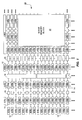
- FIG. 1 is a block diagram of a Programmable Logic Device (PLD) architecture in accordance with the present invention.
- PLD Programmable Logic Device
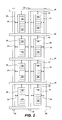
- Figure 2 is a diagram of a number of LABs interconnected by a plurality of vertical and horizontal inter-LAB lines according to the present invention.
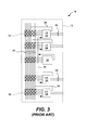
- Figure 3 is a diagram of a conventional LAB according to the prior art.
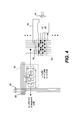
- Figure 4 illustrates a multiplexer arrangement for providing inputs to a LAB.
- Figure 5 is a logic diagram of two LABs according to one embodiment of the present invention.
- Figure 6 is a logic diagram of four LABs according to another embodiment of the present invention.
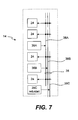
- Figure 7 is a logic diagram of a LAB according to another embodiment of the present invention.
- the PLD 10 includes a two dimensional row and column based architecture including a plurality of Input/Output elements (IOEs) 12 arranged around the periphery of the chip, a plurality of Logic Array Blocks (LABs) 14 grouped into rows and columns across the device, Random Access Memory (RAM) blocks 16 grouped into columns between certain LABs 14, Digital Signal Processing (DSP) blocks 18 grouped into columns across the device, second RAM blocks 20 also grouped into columns across the device and between certain LABs 14, and one or more M-RAM memory blocks 22, each provided at different locations across the device.
- IOEs Input/Output elements
- LABs Logic Array Blocks
- RAM Random Access Memory
- DSP Digital Signal Processing
- the LABs 14 include a predetermined number of logic elements (not visible in the figure). In various embodiments, the number of logic elements may vary from two to sixteen or more.
- the RAM blocks 16 are simple dual port memory blocks with a predetermined number of bits and additional parity bits. The RAM blocks 16 provide dedicated simple dual port or single port memory for the device.
- the DSP blocks 18 are provided for performing digital signal processing functions, such as for example, finite impulse response (FIR) and infinite impulse response (IIR) filters.
- the second RAM blocks 20 are true dual port memory blocks with memory bits and parity bits.
- the M-RAM memory blocks 22 are large true dual port memory blocks with both memory and parity bits. It should be noted that the PLD 10 is merely exemplary and in no way should be construed as limiting the invention.
- Each LAB 14 includes a plurality of logic elements 24.
- Local intra-LAB lines 26 are used to interconnect the individual logic elements 24 within each LAB 14.
- Vertical and horizontal inter-LAB lines 28 are used to interconnect the LABs 14 of the array.
- Routing drivers 30 (designated by double-sided arrows in the figure) are used to provide routing between the inter-LAB lines 28 and the local intra-LAB lines 26 of each LAB 14 respectively.
- a conventional LAB 14 includes a plurality of logic elements 24 interconnected by a plurality of LAB lines 26. As illustrated, the individual LAB lines 26 all have the same start and termination point at the top most and bottom most logic elements 24 respectively.
- a programmable interconnect pattern 32 is provided between the LAB lines 26 and the inputs to the logic elements 24. Each logic element 24 generates one or more outputs 34.
- the LAB 24 also includes one or more control signal generators 36, which generate control signals 38 that are distributed to each of the logic elements 24 within the LAB 14.
- the control signals 38 include, but are not limited to, the following: clock signals, clock enable signals, clear signals and load signals.
- the programmable interconnect pattern 32 is made up of a plurality of programmable connections (as represented by black dots in the figures). A single programmable element is provided at the intersection of the inputs to the logic elements 24 and the LAB lines 26. According to various embodiments, the programmable connections may include multiplexers, pass transistors, configurable RAM storage cells, ROM storage cells, fuses, or any other known programmable elements used in the art. It should be noted that the pattern 32 shown in Figure 2 is an example. Any suitable pattern of programmable interconnects may be used.
- the routing drivers 30 include a number of LAB Input Multiplexers (LIMs) and Driver Input multiplexers (DIMs), each designated either with an "L” (i.e., LIM), "H” (i.e., Horizontal DIM) or "V” (i.e., Vertical DIM).
- LIMs LAB Input Multiplexers
- DIMs Driver Input multiplexers
- the HDIM drives horizontal inter-LAB lines 28 and is capable of receiving inputs from some of logic elements 24 from the adjacent LABs 14 (i.e., the LABs 14 on the left and the right of the HDIM multiplexer), and other inter-LAB routing lines.
- the VDIM drives vertical inter-LAB lines 28 and is capable of receiving inputs from some of logic elements 24 in the adjacent LABs 14 and other inter-LAB routing lines.
- the two LIMs generate output signals to drive the adjacent left and right LABs 14 and each receive inputs from inter-LAB routing wires 28 and optionally the adjacent LABs 14 respectively.
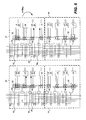
- FIG. 5 a logic diagram of two LABs for implementing redundancy with logic element granularity according to the present invention is shown.
- the diagram shows two adjacent LABs 14A and 14B, designated by the dashed lines around each.
- Both LAB 14A and 14B include a plurality of logic elements 24 and control signal generators 36, which generate control signals 38.
- LAB lines 26 are provided to connect the logic elements 24 and the control signal generators 36 of each LAB 14.
- a programmable interconnect pattern 32 is provided between the intra-LAB lines 26 and the inputs of each logic element 24.
- a LIM 30 receives inputs from the inter-LAB lines 28 and drives each of the LAB lines 26 respectively.
- the programmable interconnect pattern 32 includes two types of programmable connections. The first, designated by solid black circles, indicate programmable connections that are visible to the user. The second, designated by non-solid circles, indicate programmable connections that are invisible to the user. The invisible programmable elements are used when redundancy is engaged, unbeknownst to the user.
- Figure 6 shows the operation of redundancy in more detail.
- the LIMs 30 in each row do not have identical connectivity to the logic elements spanned by the LAB lines that they drive. This requires extra redundant connections beyond the tail connections described above.
- the left side of the diagram of Figure 6 shows a number of LIMs 30 and logic elements 24, together with two example routing paths 62 and 64.
- the control signal generators 36 and control signals 38 are deleted from the left and rights diagrams for the sake of simplification.
- the left side of the diagram shows the routing of paths 62 and 64 when redundancy is not implemented.
- the right side shows the re-routing of the signals in the situation where the second row is defective and redundancy is engaged. In this case every logic element 24 and routing resource in the second row and below is replaced by the one immediately below it, shifting each resource down by one logic element row.
- the top signal 62 which has a source that is above the defective row, continues to use the same routing elements, and so the shifting of the defective routing path uses the same intra-LAB line, but engages the routing switch in the row below. Although this could be either a user-visible or redundant switch in general, in this particular case redundancy engages a redundant switch for the connection from the intra-LAB routing to the input of the logic element.
- the source of the routing path is below the defective row, so the shifting causes the routing path to use different elements.
- the shifting causes the signal routed on a horizontal wire to shift down to a corresponding horizontal wire in the logic element row below.
- redundant routing switch is used to provide a connection from the horizontal wire to the LIM 30.
- the LIM in the row below is that the signal is routed on a different intra-LAB wire, so the path uses a connection from the shifted inter-LAB wire to the input of the logic element.
- a user-visible switch is provided, but again either a user-visible or redundant switch could be engaged depending on the details of the routing pattern.
- Figure 5 illustrates that is possible to reduce the cost of redundancy by providing LAB and local line groups that have a LIM 30 in every row that connects to that group, eliminating the extra redundant LIM 30, and only needing an extra connection on the redundant tail.
- a LIM in one row is defective, all logic at or below that row can be shifted down to the next row and there will be a corresponding LIM 30 that can drive all the logic elements that the former LIM 30 was capable of driving.
- this is not a requirement and connectivity patterns that do not have these patterns can also be defined at a cost of extra redundant switches, as shown in Figure 6 .
- the essential requirement is that in the case of a defect, all logic is shifted down by the specified redundancy pitch of the LAB lines 26, and there is a corresponding programmable connection between the corresponding LAB interconnect 26 and corresponding logic element 24.
- the programming software used in cooperation with the PLD 10 enforces a restriction that the bottom-most logic element 24 in each LAB 14 cannot use any control signal 38.
- shifting the bottom logic element 24 into the next LAB does not require access to any unavailable control signals 38, and the user-invisible connection in the LAB 14B is not required.
- This approach has a disadvantage with certain user circuits, such as counters, which require contiguous logic elements, each having access to a common clock signal. Such user designs are therefore more difficult to implement.
- the software can be modified to enforce a restriction that each LAB 14 in the array, or the logic elements 24 that are possibly shifted in a defective device, have access to the control signals 38 required by the shifted logic elements and their above neighbors.
- the LAB 14 includes a plurality of logic elements 24, a first control signal generator 38A, a second control signal generator 38B, and a redundant control signal generator 38C.
- the control signals generators 38A, 38B and 38C generate control signals 38A, 38B and 38C respectively.
- Solid circles and non-solid designate user visible connections and user invisible connections respectively between the controls signals 38A, 38B and 38C and the individual logic elements 24 of the LAB 14 respectively.
- the two control signal generators 36A and 36B define control signal generator slices, each of which provides control signals to a subset or "slice' of the logic elements 24 of the LAB.
- the control signal generator 36A provides control signal 38A to a set of logic elements 24, which in this example include the top four logic elements 24.
- the control signal generator 36B also provides control signal 38B to a set of logic elements 24, which in this case include the second, third and forth logic elements 24 of the LAB 14 shown in Figure 6 and the first logic element of the LAB below (not shown).
- the redundant generator 36C which generates signal 38C, defines a slice of the bottom two logic elements 24 of the LAB 14 shown and the top two of the LAB below.
- Generators 36A, 36B and 36C are at least capable of providing the same type of control signals, such that 36B may replace 36A, and that 36C may replace 36B.
- the redundant control signal generator 38C is provided for redundancy.
- a conventional control signal generator 36 that provides two clock signals to each of the logic elements 24 in the LAB 14.
- the control signal generator functionality is divided into two smaller generators 36A and 36B and a redundant generator 36C, each of which provides one clock signal.
- the logic elements 24 within the redundant slice may receive the redundant control signal.
- control signal slice is thus considered to be part of the logic element, using a distinct set of local lines to broadcast the control signals 38. In general, this will be true if the control signal generators are located on the same pitch as the redundancy pitch, which may motivate a redundancy pitch larger than one, as referred to earlier.
- control signal generators 38 may be used to reduce the overhead associated with redundancy.
- a set of control signal generator slices may be defined such that each slice provides for the selection and conditioning functions of one signal, or in the case of a slice that is used redundantly, the union of two functions. For example, suppose that a LAB 14 has two clear signals and two clock signals. By providing four slices, two of which provide both clock and clear functions, and one each of clock and clear functions, it is possible to ensure that a defective slice that provides only one function is shifted into the slice which is capable of providing both functions.
- the signal generators would be placed in the order clock and clear, clock, clock and clear, clear, from top to bottom, and the top two would be allocated to clock functions only, and the bottom two to clear functions only. Thus if the functions were shifted, it would always be to a signal generator capable of producing the desired signal.
- the redundancy pitch is such that the control signal generators provide each desired functions occupy all possible locations on the same pitch, then no extra generators are required. This may motivate a redundancy pitch larger than one as alluded to earlier.
- having smaller redundant regions means that the overhead required for redundant logic is decreased, thereby lowering costs.
- the lowered cost of providing redundancy translates into increase yields.
- a PLD with thirty rows might include two redundant rows using LAB level redundancy, or a 6.7% overhead.
- the same PLD with five redundant rows using the logic element redundancy scheme of the present invention the overhead is reduced to 1.7% (assuming the LABs include eight logic elements and one control signal generator having an area 1.5 times a logic element equivalent).
- the present invention allows up to five defects to be repaired versus two in the LAB level redundancy scheme.
- each redundancy region is smaller, it is less likely that two faults or defects will occur in a single region, making the die un-repairable.
- the optimal number of redundant regions will be larger for logic element level redundancy, achieving lower cost and better repair rates.
Landscapes
- Physics & Mathematics (AREA)
- Mathematical Physics (AREA)
- Engineering & Computer Science (AREA)
- Computer Hardware Design (AREA)
- Computing Systems (AREA)
- General Engineering & Computer Science (AREA)
- Logic Circuits (AREA)
- Design And Manufacture Of Integrated Circuits (AREA)
Applications Claiming Priority (1)
| Application Number | Priority Date | Filing Date | Title |
|---|---|---|---|
| US11/739,055 US7508231B2 (en) | 2007-03-09 | 2007-04-23 | Programmable logic device having redundancy with logic element granularity |
Publications (3)
| Publication Number | Publication Date |
|---|---|
| EP1986326A2 true EP1986326A2 (de) | 2008-10-29 |
| EP1986326A3 EP1986326A3 (de) | 2009-11-18 |
| EP1986326B1 EP1986326B1 (de) | 2014-05-07 |
Family
ID=39677432
Family Applications (1)
| Application Number | Title | Priority Date | Filing Date |
|---|---|---|---|
| EP08007223.4A Ceased EP1986326B1 (de) | 2007-04-23 | 2008-04-11 | Programmierbares logisches Gerät mit Redundanz mit logischer Elementengranularität |
Country Status (3)
| Country | Link |
|---|---|
| US (1) | US7508231B2 (de) |
| EP (1) | EP1986326B1 (de) |
| CN (1) | CN101295980B (de) |
Families Citing this family (5)
| Publication number | Priority date | Publication date | Assignee | Title |
|---|---|---|---|---|
| FR2951868B1 (fr) * | 2009-10-28 | 2012-04-06 | Kalray | Briques de construction d'un reseau sur puce |
| US8786308B1 (en) * | 2012-10-19 | 2014-07-22 | Altera Corporation | Method and apparatus for providing signal routing control |
| US9172373B2 (en) * | 2013-09-06 | 2015-10-27 | Globalfoundries U.S. 2 Llc | Verifying partial good voltage island structures |
| KR102557310B1 (ko) * | 2016-08-09 | 2023-07-20 | 에스케이하이닉스 주식회사 | 반도체 장치 |
| US9893732B1 (en) * | 2016-12-22 | 2018-02-13 | Intel Corporation | Techniques for bypassing defects in rows of circuits |
Citations (4)
| Publication number | Priority date | Publication date | Assignee | Title |
|---|---|---|---|---|
| US6201404B1 (en) | 1998-07-14 | 2001-03-13 | Altera Corporation | Programmable logic device with redundant circuitry |
| US20030072185A1 (en) | 2001-10-15 | 2003-04-17 | Christopher Lane | Programmable logic device with redundant circuitry |
| US6970014B1 (en) | 2001-05-06 | 2005-11-29 | Altera Corporation | Routing architecture for a programmable logic device |
| US7180324B2 (en) | 2004-05-28 | 2007-02-20 | Altera Corporation | Redundancy structures and methods in a programmable logic device |
Family Cites Families (48)
| Publication number | Priority date | Publication date | Assignee | Title |
|---|---|---|---|---|
| US4706216A (en) | 1985-02-27 | 1987-11-10 | Xilinx, Inc. | Configurable logic element |
| US5343406A (en) | 1989-07-28 | 1994-08-30 | Xilinx, Inc. | Distributed memory architecture for a configurable logic array and method for using distributed memory |
| US5260610A (en) | 1991-09-03 | 1993-11-09 | Altera Corporation | Programmable logic element interconnections for programmable logic array integrated circuits |
| US5331226A (en) | 1992-07-23 | 1994-07-19 | Xilinx, Inc. | Logic cell for field programmable gate array having optional input inverters |
| GB9223226D0 (en) | 1992-11-05 | 1992-12-16 | Algotronix Ltd | Improved configurable cellular array (cal ii) |
| US5434514A (en) * | 1992-11-19 | 1995-07-18 | Altera Corporation | Programmable logic devices with spare circuits for replacement of defects |
| EP0613249A1 (de) | 1993-02-12 | 1994-08-31 | Altera Corporation | Kundenspezifische Nachschlagetabelle mit einer verringerten Anzahl von Architektur Bits |
| US5352940A (en) | 1993-05-27 | 1994-10-04 | Altera Corporation | Ram convertible look-up table based macrocell for PLDs |
| US5438295A (en) | 1993-06-11 | 1995-08-01 | Altera Corporation | Look-up table using multi-level decode |
| US5399922A (en) | 1993-07-02 | 1995-03-21 | Altera Corporation | Macrocell comprised of two look-up tables and two flip-flops |
| US5689195A (en) | 1995-05-17 | 1997-11-18 | Altera Corporation | Programmable logic array integrated circuit devices |
| US5606266A (en) | 1994-11-04 | 1997-02-25 | Altera Corporation | Programmable logic array integrated circuits with enhanced output routing |
| US5815726A (en) | 1994-11-04 | 1998-09-29 | Altera Corporation | Coarse-grained look-up table architecture |
| US5821773A (en) | 1995-09-06 | 1998-10-13 | Altera Corporation | Look-up table based logic element with complete permutability of the inputs to the secondary signals |
| US5835998A (en) | 1996-04-04 | 1998-11-10 | Altera Corporation | Logic cell for programmable logic devices |
| US6107822A (en) | 1996-04-09 | 2000-08-22 | Altera Corporation | Logic element for a programmable logic integrated circuit |
| US6034540A (en) | 1997-04-08 | 2000-03-07 | Altera Corporation | Programmable logic integrated circuit architecture incorporating a lonely register |
| US5825202A (en) | 1996-09-26 | 1998-10-20 | Xilinx, Inc. | Integrated circuit with field programmable and application specific logic areas |
| US5999016A (en) | 1996-10-10 | 1999-12-07 | Altera Corporation | Architectures for programmable logic devices |
| US6323682B1 (en) | 1996-11-22 | 2001-11-27 | Xilinx, Inc. | FPGA architecture with wide function multiplexers |
| US6133751A (en) | 1998-08-05 | 2000-10-17 | Xilinx, Inc. | Programmable delay element |
| US6249149B1 (en) | 1997-01-23 | 2001-06-19 | Altera Corporation | Apparatus and method for centralized generation of an enabled clock signal for a logic array block of a programmable logic device |
| US6091258A (en) * | 1997-02-05 | 2000-07-18 | Altera Corporation | Redundancy circuitry for logic circuits |
| US5999015A (en) | 1997-02-20 | 1999-12-07 | Altera Corporation | Logic region resources for programmable logic devices |
| US5920202A (en) | 1997-02-26 | 1999-07-06 | Xilinx, Inc. | Configurable logic element with ability to evaluate five and six input functions |
| US6201410B1 (en) | 1997-02-26 | 2001-03-13 | Xilinx, Inc. | Wide logic gate implemented in an FPGA configurable logic element |
| US6150837A (en) | 1997-02-28 | 2000-11-21 | Actel Corporation | Enhanced field programmable gate array |
| US5923185A (en) | 1997-03-12 | 1999-07-13 | Xilinx, Inc. | Logic circuit programmable to implement at least two logic functions |
| US6069487A (en) | 1997-10-14 | 2000-05-30 | Altera Corporation | Programmable logic device circuitry for improving multiplier speed and/or efficiency |
| US6084427A (en) | 1998-05-19 | 2000-07-04 | Altera Corporation | Programmable logic devices with enhanced multiplexing capabilities |
| US6069490A (en) | 1997-12-02 | 2000-05-30 | Xilinx, Inc. | Routing architecture using a direct connect routing mesh |
| US6167558A (en) | 1998-02-20 | 2000-12-26 | Xilinx, Inc. | Method for tolerating defective logic blocks in programmable logic devices |
| US6020756A (en) | 1998-03-03 | 2000-02-01 | Xilinx, Inc. | Multiplexer enhanced configurable logic block |
| US6066960A (en) | 1998-05-21 | 2000-05-23 | Altera Corporation | Programmable logic device having combinational logic at inputs to logic elements within logic array blocks |
| US6211696B1 (en) | 1998-05-30 | 2001-04-03 | Cypress Semiconductor Corp. | Hybrid product term and look-up table-based programmable logic device with improved speed and area efficiency |
| US6184707B1 (en) | 1998-10-07 | 2001-02-06 | Altera Corporation | Look-up table based logic element with complete permutability of the inputs to the secondary signals |
| US6118300A (en) | 1998-11-24 | 2000-09-12 | Xilinx, Inc. | Method for implementing large multiplexers with FPGA lookup tables |
| US6400180B2 (en) | 1999-02-25 | 2002-06-04 | Xilinix, Inc. | Configurable lookup table for programmable logic devices |
| EP1162747B1 (de) * | 2000-04-26 | 2012-02-29 | Altera Corporation | Leitungssegmentierung in programmierbaren logischen Vorrichtungen mit redundanten Schaltungen |
| US6538470B1 (en) | 2000-09-18 | 2003-03-25 | Altera Corporation | Devices and methods with programmable logic and digital signal processing regions |
| US6526559B2 (en) * | 2001-04-13 | 2003-02-25 | Interface & Control Systems, Inc. | Method for creating circuit redundancy in programmable logic devices |
| US6895570B2 (en) * | 2001-05-06 | 2005-05-17 | Altera Corporation | System and method for optimizing routing lines in a programmable logic device |
| CN100489797C (zh) * | 2001-10-11 | 2009-05-20 | 阿尔特拉公司 | 可编程逻辑设备上的错误检测 |
| US6545501B1 (en) * | 2001-12-10 | 2003-04-08 | International Business Machines Corporation | Method and system for use of a field programmable function within a standard cell chip for repair of logic circuits |
| US6937064B1 (en) | 2002-10-24 | 2005-08-30 | Altera Corporation | Versatile logic element and logic array block |
| US7111213B1 (en) * | 2002-12-10 | 2006-09-19 | Altera Corporation | Failure isolation and repair techniques for integrated circuits |
| US7215140B1 (en) * | 2003-05-30 | 2007-05-08 | Altera Corporation | Programmable logic device having regions of non-repairable circuitry within an array of repairable circuitry and associated configuration hardware and method |
| US7061268B1 (en) | 2004-03-15 | 2006-06-13 | Altera Corporation | Initializing a carry chain in a programmable logic device |
-
2007
- 2007-04-23 US US11/739,055 patent/US7508231B2/en active Active
-
2008
- 2008-04-11 EP EP08007223.4A patent/EP1986326B1/de not_active Ceased
- 2008-04-23 CN CN2008100912558A patent/CN101295980B/zh active Active
Patent Citations (6)
| Publication number | Priority date | Publication date | Assignee | Title |
|---|---|---|---|---|
| US6201404B1 (en) | 1998-07-14 | 2001-03-13 | Altera Corporation | Programmable logic device with redundant circuitry |
| US6344755B1 (en) | 1998-07-14 | 2002-02-05 | Altera Corporation | Programmable logic device with redundant circuitry |
| US6970014B1 (en) | 2001-05-06 | 2005-11-29 | Altera Corporation | Routing architecture for a programmable logic device |
| US20030072185A1 (en) | 2001-10-15 | 2003-04-17 | Christopher Lane | Programmable logic device with redundant circuitry |
| US6965249B2 (en) | 2001-10-15 | 2005-11-15 | Altera Corporation | Programmable logic device with redundant circuitry |
| US7180324B2 (en) | 2004-05-28 | 2007-02-20 | Altera Corporation | Redundancy structures and methods in a programmable logic device |
Also Published As
| Publication number | Publication date |
|---|---|
| CN101295980A (zh) | 2008-10-29 |
| US20080218197A1 (en) | 2008-09-11 |
| CN101295980B (zh) | 2012-06-20 |
| US7508231B2 (en) | 2009-03-24 |
| EP1986326B1 (de) | 2014-05-07 |
| EP1986326A3 (de) | 2009-11-18 |
Similar Documents
| Publication | Publication Date | Title |
|---|---|---|
| Cheatham et al. | A survey of fault tolerant methodologies for FPGAs | |
| US6600337B2 (en) | Line segmentation in programmable logic devices having redundancy circuitry | |
| CN1117432C (zh) | 可缩放的多层互联结构 | |
| US6163168A (en) | Efficient interconnect network for use in FPGA device having variable grain architecture | |
| CN108228395B (zh) | 用于绕开电路行中的缺陷的技术 | |
| JP5485962B2 (ja) | 電子デバイス | |
| EP0824792B1 (de) | Flächenanordnung für skalierbare mehrlagige verbindungsarchitektur | |
| US20100060309A1 (en) | Multi-row block supporting row level redundancy in a pld | |
| US7902855B1 (en) | Repairable IO in an integrated circuit | |
| EP1986326B1 (de) | Programmierbares logisches Gerät mit Redundanz mit logischer Elementengranularität | |
| US6927601B1 (en) | Flexible macrocell interconnect | |
| EP2113836B1 (de) | Flexible Addierschaltungen mit schneller Übertragskette | |
| US7459932B1 (en) | Programmable logic device having logic modules with improved register capabilities | |
| US7456653B2 (en) | Programmable logic device having logic array block interconnect lines that can interconnect logic elements in different logic blocks | |
| US20060109027A1 (en) | Programmable logic cell | |
| US7345506B1 (en) | Redundancy method and software to provide improved interconnect efficiency for programmable logic devices | |
| US9768784B2 (en) | Transformable logic and routing structures for datapath optimization | |
| EP4683228A1 (de) | Programmierbare logische vorrichtung und fpga mit dieser programmierbaren logischen vorrichtung | |
| JP2026015242A (ja) | プログラマブル論理回路装置及びこのプログラマブル論理回路を用いたfpga |
Legal Events
| Date | Code | Title | Description |
|---|---|---|---|
| PUAI | Public reference made under article 153(3) epc to a published international application that has entered the european phase |
Free format text: ORIGINAL CODE: 0009012 |
|
| AK | Designated contracting states |
Kind code of ref document: A2 Designated state(s): AT BE BG CH CY CZ DE DK EE ES FI FR GB GR HR HU IE IS IT LI LT LU LV MC MT NL NO PL PT RO SE SI SK TR |
|
| AX | Request for extension of the european patent |
Extension state: AL BA MK RS |
|
| PUAL | Search report despatched |
Free format text: ORIGINAL CODE: 0009013 |
|
| AK | Designated contracting states |
Kind code of ref document: A3 Designated state(s): AT BE BG CH CY CZ DE DK EE ES FI FR GB GR HR HU IE IS IT LI LT LU LV MC MT NL NO PL PT RO SE SI SK TR |
|
| AX | Request for extension of the european patent |
Extension state: AL BA MK RS |
|
| 17P | Request for examination filed |
Effective date: 20100518 |
|
| AKX | Designation fees paid |
Designated state(s): DE |
|
| GRAP | Despatch of communication of intention to grant a patent |
Free format text: ORIGINAL CODE: EPIDOSNIGR1 |
|
| INTG | Intention to grant announced |
Effective date: 20131121 |
|
| GRAS | Grant fee paid |
Free format text: ORIGINAL CODE: EPIDOSNIGR3 |
|
| GRAA | (expected) grant |
Free format text: ORIGINAL CODE: 0009210 |
|
| AK | Designated contracting states |
Kind code of ref document: B1 Designated state(s): DE |
|
| REG | Reference to a national code |
Ref country code: DE Ref legal event code: R096 Ref document number: 602008031976 Country of ref document: DE Effective date: 20140626 |
|
| REG | Reference to a national code |
Ref country code: DE Ref legal event code: R097 Ref document number: 602008031976 Country of ref document: DE |
|
| PLBE | No opposition filed within time limit |
Free format text: ORIGINAL CODE: 0009261 |
|
| STAA | Information on the status of an ep patent application or granted ep patent |
Free format text: STATUS: NO OPPOSITION FILED WITHIN TIME LIMIT |
|
| 26N | No opposition filed |
Effective date: 20150210 |
|
| REG | Reference to a national code |
Ref country code: DE Ref legal event code: R097 Ref document number: 602008031976 Country of ref document: DE Effective date: 20150210 |
|
| REG | Reference to a national code |
Ref country code: DE Ref legal event code: R082 Ref document number: 602008031976 Country of ref document: DE Representative=s name: DENNEMEYER & ASSOCIATES S.A., DE Ref country code: DE Ref legal event code: R081 Ref document number: 602008031976 Country of ref document: DE Owner name: TAHOE RESEARCH, LTD., IE Free format text: FORMER OWNER: ALTERA CORP., SAN JOSE, CALIF., US Ref country code: DE Ref legal event code: R081 Ref document number: 602008031976 Country of ref document: DE Owner name: INTEL CORPORATION, SANTA CLARA, US Free format text: FORMER OWNER: ALTERA CORP., SAN JOSE, CALIF., US Ref country code: DE Ref legal event code: R082 Ref document number: 602008031976 Country of ref document: DE Ref country code: DE Ref legal event code: R082 Ref document number: 602008031976 Country of ref document: DE Representative=s name: DENNEMEYER & ASSOCIATES RECHTSANWALTSGESELLSCH, DE |
|
| REG | Reference to a national code |
Ref country code: DE Ref legal event code: R081 Ref document number: 602008031976 Country of ref document: DE Owner name: TAHOE RESEARCH, LTD., IE Free format text: FORMER OWNER: INTEL CORPORATION, SANTA CLARA, CA, US Ref country code: DE Ref legal event code: R082 Ref document number: 602008031976 Country of ref document: DE Representative=s name: DENNEMEYER & ASSOCIATES S.A., DE Ref country code: DE Ref legal event code: R082 Ref document number: 602008031976 Country of ref document: DE Representative=s name: DENNEMEYER & ASSOCIATES RECHTSANWALTSGESELLSCH, DE |
|
| PGFP | Annual fee paid to national office [announced via postgrant information from national office to epo] |
Ref country code: DE Payment date: 20240418 Year of fee payment: 17 |
|
| REG | Reference to a national code |
Ref country code: DE Ref legal event code: R082 Ref document number: 602008031976 Country of ref document: DE Representative=s name: DENNEMEYER & ASSOCIATES RECHTSANWALTSGESELLSCH, DE |
|
| REG | Reference to a national code |
Ref country code: DE Ref legal event code: R119 Ref document number: 602008031976 Country of ref document: DE |
|
| PG25 | Lapsed in a contracting state [announced via postgrant information from national office to epo] |
Ref country code: DE Free format text: LAPSE BECAUSE OF NON-PAYMENT OF DUE FEES Effective date: 20251104 |