EP1986038A2 - Liquid crystal displa panel and fabricating method thereof - Google Patents
Liquid crystal displa panel and fabricating method thereof Download PDFInfo
- Publication number
- EP1986038A2 EP1986038A2 EP07123606A EP07123606A EP1986038A2 EP 1986038 A2 EP1986038 A2 EP 1986038A2 EP 07123606 A EP07123606 A EP 07123606A EP 07123606 A EP07123606 A EP 07123606A EP 1986038 A2 EP1986038 A2 EP 1986038A2
- Authority
- EP
- European Patent Office
- Prior art keywords
- spacer
- integrated
- planarizing layer
- liquid crystal
- sub pixels
- Prior art date
- Legal status (The legal status is an assumption and is not a legal conclusion. Google has not performed a legal analysis and makes no representation as to the accuracy of the status listed.)
- Granted
Links
Images


Classifications
-
- G—PHYSICS
- G02—OPTICS
- G02F—OPTICAL DEVICES OR ARRANGEMENTS FOR THE CONTROL OF LIGHT BY MODIFICATION OF THE OPTICAL PROPERTIES OF THE MEDIA OF THE ELEMENTS INVOLVED THEREIN; NON-LINEAR OPTICS; FREQUENCY-CHANGING OF LIGHT; OPTICAL LOGIC ELEMENTS; OPTICAL ANALOGUE/DIGITAL CONVERTERS
- G02F1/00—Devices or arrangements for the control of the intensity, colour, phase, polarisation or direction of light arriving from an independent light source, e.g. switching, gating or modulating; Non-linear optics
- G02F1/01—Devices or arrangements for the control of the intensity, colour, phase, polarisation or direction of light arriving from an independent light source, e.g. switching, gating or modulating; Non-linear optics for the control of the intensity, phase, polarisation or colour
- G02F1/13—Devices or arrangements for the control of the intensity, colour, phase, polarisation or direction of light arriving from an independent light source, e.g. switching, gating or modulating; Non-linear optics for the control of the intensity, phase, polarisation or colour based on liquid crystals, e.g. single liquid crystal display cells
- G02F1/133—Constructional arrangements; Operation of liquid crystal cells; Circuit arrangements
- G02F1/1333—Constructional arrangements; Manufacturing methods
- G02F1/1339—Gaskets; Spacers; Sealing of cells
- G02F1/13394—Gaskets; Spacers; Sealing of cells spacers regularly patterned on the cell subtrate, e.g. walls, pillars
-
- G—PHYSICS
- G02—OPTICS
- G02F—OPTICAL DEVICES OR ARRANGEMENTS FOR THE CONTROL OF LIGHT BY MODIFICATION OF THE OPTICAL PROPERTIES OF THE MEDIA OF THE ELEMENTS INVOLVED THEREIN; NON-LINEAR OPTICS; FREQUENCY-CHANGING OF LIGHT; OPTICAL LOGIC ELEMENTS; OPTICAL ANALOGUE/DIGITAL CONVERTERS
- G02F1/00—Devices or arrangements for the control of the intensity, colour, phase, polarisation or direction of light arriving from an independent light source, e.g. switching, gating or modulating; Non-linear optics
- G02F1/01—Devices or arrangements for the control of the intensity, colour, phase, polarisation or direction of light arriving from an independent light source, e.g. switching, gating or modulating; Non-linear optics for the control of the intensity, phase, polarisation or colour
- G02F1/13—Devices or arrangements for the control of the intensity, colour, phase, polarisation or direction of light arriving from an independent light source, e.g. switching, gating or modulating; Non-linear optics for the control of the intensity, phase, polarisation or colour based on liquid crystals, e.g. single liquid crystal display cells
- G02F1/133—Constructional arrangements; Operation of liquid crystal cells; Circuit arrangements
- G02F1/1333—Constructional arrangements; Manufacturing methods
- G02F1/1335—Structural association of cells with optical devices, e.g. polarisers or reflectors
-
- G—PHYSICS
- G02—OPTICS
- G02F—OPTICAL DEVICES OR ARRANGEMENTS FOR THE CONTROL OF LIGHT BY MODIFICATION OF THE OPTICAL PROPERTIES OF THE MEDIA OF THE ELEMENTS INVOLVED THEREIN; NON-LINEAR OPTICS; FREQUENCY-CHANGING OF LIGHT; OPTICAL LOGIC ELEMENTS; OPTICAL ANALOGUE/DIGITAL CONVERTERS
- G02F1/00—Devices or arrangements for the control of the intensity, colour, phase, polarisation or direction of light arriving from an independent light source, e.g. switching, gating or modulating; Non-linear optics
- G02F1/01—Devices or arrangements for the control of the intensity, colour, phase, polarisation or direction of light arriving from an independent light source, e.g. switching, gating or modulating; Non-linear optics for the control of the intensity, phase, polarisation or colour
- G02F1/13—Devices or arrangements for the control of the intensity, colour, phase, polarisation or direction of light arriving from an independent light source, e.g. switching, gating or modulating; Non-linear optics for the control of the intensity, phase, polarisation or colour based on liquid crystals, e.g. single liquid crystal display cells
- G02F1/133—Constructional arrangements; Operation of liquid crystal cells; Circuit arrangements
- G02F1/1333—Constructional arrangements; Manufacturing methods
- G02F1/1339—Gaskets; Spacers; Sealing of cells
-
- G—PHYSICS
- G02—OPTICS
- G02F—OPTICAL DEVICES OR ARRANGEMENTS FOR THE CONTROL OF LIGHT BY MODIFICATION OF THE OPTICAL PROPERTIES OF THE MEDIA OF THE ELEMENTS INVOLVED THEREIN; NON-LINEAR OPTICS; FREQUENCY-CHANGING OF LIGHT; OPTICAL LOGIC ELEMENTS; OPTICAL ANALOGUE/DIGITAL CONVERTERS
- G02F1/00—Devices or arrangements for the control of the intensity, colour, phase, polarisation or direction of light arriving from an independent light source, e.g. switching, gating or modulating; Non-linear optics
- G02F1/01—Devices or arrangements for the control of the intensity, colour, phase, polarisation or direction of light arriving from an independent light source, e.g. switching, gating or modulating; Non-linear optics for the control of the intensity, phase, polarisation or colour
- G02F1/15—Devices or arrangements for the control of the intensity, colour, phase, polarisation or direction of light arriving from an independent light source, e.g. switching, gating or modulating; Non-linear optics for the control of the intensity, phase, polarisation or colour based on an electrochromic effect
- G02F1/153—Constructional details
- G02F1/161—Gaskets; Spacers; Sealing of cells; Filling or closing of cells
-
- G—PHYSICS
- G02—OPTICS
- G02F—OPTICAL DEVICES OR ARRANGEMENTS FOR THE CONTROL OF LIGHT BY MODIFICATION OF THE OPTICAL PROPERTIES OF THE MEDIA OF THE ELEMENTS INVOLVED THEREIN; NON-LINEAR OPTICS; FREQUENCY-CHANGING OF LIGHT; OPTICAL LOGIC ELEMENTS; OPTICAL ANALOGUE/DIGITAL CONVERTERS
- G02F1/00—Devices or arrangements for the control of the intensity, colour, phase, polarisation or direction of light arriving from an independent light source, e.g. switching, gating or modulating; Non-linear optics
- G02F1/01—Devices or arrangements for the control of the intensity, colour, phase, polarisation or direction of light arriving from an independent light source, e.g. switching, gating or modulating; Non-linear optics for the control of the intensity, phase, polarisation or colour
- G02F1/13—Devices or arrangements for the control of the intensity, colour, phase, polarisation or direction of light arriving from an independent light source, e.g. switching, gating or modulating; Non-linear optics for the control of the intensity, phase, polarisation or colour based on liquid crystals, e.g. single liquid crystal display cells
- G02F1/133—Constructional arrangements; Operation of liquid crystal cells; Circuit arrangements
- G02F1/1333—Constructional arrangements; Manufacturing methods
- G02F1/1335—Structural association of cells with optical devices, e.g. polarisers or reflectors
- G02F1/133509—Filters, e.g. light shielding masks
- G02F1/133514—Colour filters
- G02F1/133519—Overcoatings
-
- G—PHYSICS
- G02—OPTICS
- G02F—OPTICAL DEVICES OR ARRANGEMENTS FOR THE CONTROL OF LIGHT BY MODIFICATION OF THE OPTICAL PROPERTIES OF THE MEDIA OF THE ELEMENTS INVOLVED THEREIN; NON-LINEAR OPTICS; FREQUENCY-CHANGING OF LIGHT; OPTICAL LOGIC ELEMENTS; OPTICAL ANALOGUE/DIGITAL CONVERTERS
- G02F1/00—Devices or arrangements for the control of the intensity, colour, phase, polarisation or direction of light arriving from an independent light source, e.g. switching, gating or modulating; Non-linear optics
- G02F1/01—Devices or arrangements for the control of the intensity, colour, phase, polarisation or direction of light arriving from an independent light source, e.g. switching, gating or modulating; Non-linear optics for the control of the intensity, phase, polarisation or colour
- G02F1/13—Devices or arrangements for the control of the intensity, colour, phase, polarisation or direction of light arriving from an independent light source, e.g. switching, gating or modulating; Non-linear optics for the control of the intensity, phase, polarisation or colour based on liquid crystals, e.g. single liquid crystal display cells
- G02F1/133—Constructional arrangements; Operation of liquid crystal cells; Circuit arrangements
- G02F1/1333—Constructional arrangements; Manufacturing methods
- G02F1/1335—Structural association of cells with optical devices, e.g. polarisers or reflectors
- G02F1/13363—Birefringent elements, e.g. for optical compensation
-
- G—PHYSICS
- G02—OPTICS
- G02F—OPTICAL DEVICES OR ARRANGEMENTS FOR THE CONTROL OF LIGHT BY MODIFICATION OF THE OPTICAL PROPERTIES OF THE MEDIA OF THE ELEMENTS INVOLVED THEREIN; NON-LINEAR OPTICS; FREQUENCY-CHANGING OF LIGHT; OPTICAL LOGIC ELEMENTS; OPTICAL ANALOGUE/DIGITAL CONVERTERS
- G02F2201/00—Constructional arrangements not provided for in groups G02F1/00 - G02F7/00
- G02F2201/48—Flattening arrangements
Definitions
- the present invention relates to a liquid crystal display panel, and more particularly, to a liquid crystal display panel and a method for fabricating the same, wherein a fabrication process of a color filter array can be simplified and an adhesion process of a compensation film can be shortened.
- Liquid crystal display devices control light transmittance of liquid crystal cells according to a video signal to render the liquid crystal cells to display an image corresponding to the video signal on a liquid crystal display panel arranged in the form of a matrix.
- liquid crystal display devices include a liquid crystal display panel, where liquid crystal cells are arranged in the form of an active matrix, and driving circuits to drive the LCD panel.
- the liquid crystal display panel includes a upper substrate 2 where a color filter array is formed, a lower substrate 22 where a thin film transistor array 22 is formed, and a liquid crystal 11 interposed into the cell gap between the upper substrate 2 and the lower substrate 22, a lower polarizing film 21 adhered to a light-incident plane, a upper polarizing film 1 adhered to a light-emitting plane, and a compensation film 3 interposed between the lower upper substrate 2 and the upper polarizing film 1.
- the compensation film 3 may be further arranged between the lower polarizing film 21 and the lower substrate 22.
- the color filter array includes a black matrix 4, a color filter 6, a planarizing layer 7 and an upper alignment layer 8 arranged on the upper substrate 2.
- the thin film transistor array includes a thin film transistor (hereinafter, referred to simply as "TFT"), a common electrode 13, a pixel electrode 18 and a lower alignment layer 28 arranged on the lower substrate 22.
- TFT thin film transistor
- the upper substrate 2 and the lower substrate 22 are joined to each other such that the color filter array faces the thin film transistor array.
- the spacer 10 serves to maintain the cell gap between the two substrates.
- the black matrix 4 overlaps a region corresponding to the TFT of the thin film transistor array and a region corresponding to gate lines and data lines (not shown), and partitions sub pixels.
- the color filter 6 is formed at each sub pixel partitioned by the black matrix 4.
- the sub pixel includes repeated filter patterns of R, G and B sub pixels, and may further include a W sub pixel to improve brightness.
- the color filter 6 includes R, G and B color filters, which render red, green and blue, respectively.
- the sub pixel further includes a W sub pixel
- the color filter 6 further includes a W color filter pattern at the W sub pixel.
- the planarizing layer 7 is formed to cover the color filter and levels out the upper substrate 2.
- the TFT includes a gate electrode 12 connected to a gate line (not shown), a gate insulating film 24, a semiconductor pattern 14 overlapping the gate electrode 12, and a source electrode 40 in ohmic contact with the semiconductor pattern 14 and connected to the data line (not shown) that crosses the gate line, and a drain electrode 17 spaced apart from the source electrode 40 and arranged to be in ohmic contact with the semiconductor pattern 14.
- the TFT supplies a pixel signal through a data line to a pixel electrode 18, in response to a scanning signal through the gate line.
- the pixel electrode 18 is in contact with the drain electrode 17 of the TFT through a contact hole in a protective film 26.
- a common electrode 13 is formed in the form of a stripe such that it is alternately arranged with the pixel electrode 18.
- the common electrode 13 applies a common voltage which is a base voltage of liquid crystal driving.
- An upper alignment film 8 and a lower alignment film 28 render the liquid crystal 11 to be uniformly aligned.
- the liquid crystal 11 rotates in accordance with an electric field generated by the common voltage supplied from the common electrode 13 and the pixel voltage supplied from the pixel electrode 18 to control light-transmittance.
- An upper polarizing film 1 and a lower polarizing film 21 allow non-polarized incident lights to be linearly polarized.
- Light incident to the LCD panel is linearly polarized through the lower polarizing film 21 and is transmitted to the liquid crystal 11 having refractive index anisotropy. At the same time, the light is vertically or obliquely transmitted to the liquid crystal 11.
- Lights that transmit the upper polarized film in respective directions have different retardation values due to the liquid crystal 11, thus causing phase-difference.
- the phase-difference resulting from the transmission directions varies the properties of the transmitted lights, according to a viewing angle.
- the compensation film 3 offsets the optical phase-difference and thus improves viewing angle properties of the LCD panel.
- FIGs. 2A and 2D are sectional views sequentially illustrating a method for fabricating the color filter array shown in FIG. 1 .
- An opaque resin is applied over the entire surface of an upper substrate 2 and is then patterned by photolithographic and etching processes using a first mask, to form a black matrix 4, as shown in FIG. 2A .
- a red resin is deposited on the upper substrate 2 including the black matrix 4 and is then patterned by photolithographic and etching processes using a second mask, to form a red color filter pattern R, as shown in FIG. 2B .
- a green, blue, and white color filter patterns G, B and W are sequentially formed using a third, fourth, and fifth mask, respectively.
- Green, blue and transparent resins are used to form the green, blue, and white color filter patterns G, B and W, respectively.
- the planarizing layer 7 cannot offset the step between W sub pixels. Accordingly, it is preferable to form the white color filter pattern W, in terms of efficient planarization of the upper substrate 1, where the color filter 6 is formed.
- planarizing layer 7 eliminates the topology of the sub pixels which is caused by the black matrix 2 composed of an opaque resin.
- a spacer material is applied over the entire surface of the planarizing layer 7 and is then patterned by photolithographic and etching processes using a sixth mask, to form a spacer 10, as shown in FIG. 2D .
- each of the mask processes comprises a photolithographic process, which is a photographic process including a series of the steps of involving applying, exposing and developing a photoresist.
- the photolithographic process requires long process time and high equipment costs.
- the upper substrate 1 including the thin film transistor array is joined to the lower substrate 21 including the color filter array, the liquid crystal 11 is interposed into the cell gap, and a compensation film 3 and polarized films 1 and 2 are adhered.
- the compensation film 3 improves display quality of the LCD panel, but disadvantageously causing increases in material costs and fabrication process time.
- the present invention is directed to a liquid crystal display panel and a method for fabricating the same that substantially obviate one or more problems due to limitations and disadvantages of the related art.
- An object of the present invention is to provide a liquid crystal display (LCD) panel and a method for fabricating the same, wherein a fabrication process of a color filter array can be simplified and an adhesion process of a compensation film can be shortened.
- LCD liquid crystal display
- a liquid crystal display panel comprises: a black matrix partitioning sub pixels; a plurality of color filters formed at respective sub pixels; and a spacer-integrated planarizing layer arranged on the color filters and the black matrix, wherein the spacer-integrated planarizing layer includes a planarized surface at each of the sub pixels and a spacer pattern integrated with the planarized surface and protrudes at the black matrix, and wherein the spacer-integrated planarizing layer is composed of a liquid crystalline material to offset phase retardation difference of light.
- a method for fabricating a liquid crystal display panel comprising: forming a black matrix partitioning sub pixels; forming a plurality of color filters at respective sub pixels; forming a spacer-integrated planarizing layer on the color filters and the black matrix, wherein the spacer-integrated planarizing layer includes a planarized surface at each of the sub pixels and a spacer pattern integrated with the planarized surface and protrudes at the black matrix, and wherein the spacer-integrated planarizing layer is composed of a liquid crystalline material to offset the phase retardation of light.
- the liquid crystalline material includes reactive mesogen.
- the step of forming the spacer-integrated planarizing layer includes: preparing a resin comprising 30 to 40 vol% of a mono-functional monomer, 20 to 40 vol% of a di-functional monomer, 0 to 20 vol% of a tri-functional monomer, 10 vol% or more of the reactive mesogen and 1 to 3 vol% of a photoinitiator, based on a total 100 vol% of the resin; molding the resin using a soft mold having a groove/protrusion patterns corresponding to the spacer pattern and the planarizing surface; and the photo-curing the resin.
- Each of the sub pixels includes red, green, blue and transparent sub pixels and the color filters are formed in the red, green and blue sub pixels, other than the transparent sub pixel.
- the method further comprises forming an alignment film between the color filters and the spacer-integrated planarizing layer to align the reactive mesogen.
- the method further comprises forming a common electrode between the color filters and the spacer-integrated planarizing layer.
- the method further comprises forming an alignment film between the common electrode and the spacer-integrated planarizing layer.
- FIG. 1 is a sectional view illustrating a conventional liquid crystal display panel
- FIGs. 2A and 2D are sectional views sequentially illustrating a process for fabricating a color filter array of a conventional liquid crystal display panel
- FIG. 3 is a sectional view illustrating a liquid crystal display panel according to one embodiment of the present invention.
- FIG. 4A to 4C are sectional views more specifically illustrating a method for fabricating the color filter array shown in FIG. 3 ;
- FIGs. 5A to 5C are sectional views more specifically illustrating a method for fabricating an optical compensation spacer of the color filter array shown in FIG. 3 ;
- FIG. 6 is a view illustrating one embodiment of reactive mesogen.
- the LCD panel includes a upper substrate 102 where a color filter array is formed, a lower substrate 122 where a thin film transistor array is formed, and a liquid crystal 111 interposed into the cell gap between the upper substrate 102 and the lower substrate 122, a lower polarizing film 121 adhered to a light-incident plane, and a upper polarizing film 101 adhered to a light-emitting plane.
- the color filter array includes a black matrix 104, a color filter 106, a spacer-integrated planarizing layer 100 and an upper alignment layer 108 arranged on the upper substrate 102.
- the thin film transistor array includes a thin film transistor (hereinafter, referred to simply as "TFT"), a common electrode 113, a pixel electrode 118 and a lower alignment layer 128 arranged on the lower substrate 122.
- TFT thin film transistor
- the upper substrate 102 and the lower substrate 122 are joined to each other such that the color filter array faces the thin film transistor array.
- a cell gap is maintained by a spacer-integrated planarizing layer 100 between the two substrates.
- the black matrix 104 overlaps a region corresponding to the TFT of the thin film transistor array and a region corresponding to gate and data lines (not shown), and partitions sub pixels.
- the black matrix 104 serves to prevent leakage of lights and increase a contrast by absorbing external lights.
- the color filter 106 is formed at each sub pixel partitioned by the black matrix 4.
- the sub pixel includes R, G and B sub pixels, and may further include a W sub pixel in order to improve brightness.
- the color filter 106 includes R, G, and B color filter patterns arranged in the R, G and B sub pixels, respectively, other than the transparent sub pixel W.
- the R, G, and B color filter patterns render red, green and blue, respectively.
- the spacer-integrated planarizing layer 100 eliminates the topology caused by the black matrix 104 and the W sub pixel where there is no color filter 106.
- the spacer-integrated planarizing layer 100 is composed of a liquid crystalline material and thus offsets the phase retardation difference of light that transmit liquid crystal cells in a large viewing angle range. Similar to a bulk liquid crystal, the liquid crystalline material included in the spacer-integrated planarizing layer 100 contains a reactive mesogen which has a constant (not variable) phase retardation value.
- the spacer-integrated planarizing layer 100 includes a planarized surface in an effective display side at respective sub pixels, and a spacer pattern integrated with the planarized surface and protrudes from the boundary, i.e., the black matrix 104, between adjacent two sub pixels.
- the spacer-integrated planarizing layer 100 acts as not only a planarizing layer to level out the sub pixel, but also as a spacer to maintain the cell gap.
- the planarized surface of the spacer-integrated planarizing layer 100 enables the upper alignment film 108 to be evenly and uniformly formed on the effective display side at each sub pixel, thus rendering the liquid crystal 111 to be uniformly aligned.
- the reactive mesogen has liquid crystalline properties. Accordingly, control over the refractive index anisotropy and thickness of the reactive mesogen enables control of phase retardation values.
- the reactive mesogen may be included in the alignment film which allows the reactive mesogen to be aligned in conformity with optical properties of the spacer-integrated planarizing layer 100.
- the reactive mesogen is not aligned with the alignment film, it is self-aligned to have the negative C-plate property. For this reason, it is unnecessary to form an additional alignment film.
- the LCD panel according to the embodiments of the present invention includes further an alignment film to align the reactive mesogen.
- the LCD panel includes further an alignment film arranged between the color filter 106 and the spacer-integrated planarizing layer 100.
- the TFT includes a gate electrode 112 connected to a gate line (not shown), a gate insulating film 124, a semiconductor pattern 114 overlapping the gate electrode 112, and a source electrode 140 in ohmic contact with the semiconductor pattern 114 and connected to the data line (not shown) that crosses the gate line, and a drain electrode 117 spaced apart from the source electrode 140 and arranged to be in ohmic contact with the semiconductor pattern 114.
- the TFT supplies a pixel signal through a data line to a pixel electrode 118, in response to a scanning signal through the gate line.
- the pixel electrode 118 is in contact with the drain electrode 117 through a contact hole in a protective film 126.
- a common electrode 113 is formed in the form of a stripe such that it is alternatively arranged with the pixel electrode 118.
- the common electrode 113 applies a common voltage which is a base voltage of liquid crystal driving.
- An upper alignment film 108 and a lower alignment film 128 render the liquid crystal 111 to be uniformly aligned.
- the liquid crystal 111 rotates in accordance with an electric field generated by the common voltage supplied from the common electrode 113 and the pixel voltage supplied from the pixel electrode 118 to control light-transmittance.
- An upper polarizing film 101 and a lower polarizing film 121 allow non-polarized incident light to be linearly polarized.
- Light incident to the LCD panel is linearly polarized through the lower polarizing film 121 and transmitted to the liquid crystal 111 having refractive index anisotropy. At the same time, the light is vertically or obliquely transmitted to the liquid crystal 111.
- Lights that transmit the upper polarized film in respective directions have different retardation values by the liquid crystal 111, thus causing phase-difference.
- the phase retardation difference resulting from the transmission directions varies the properties of the transmitted lights according to a viewing angle.
- the spacer-integrated planarizing layer 100 offsets the optical phase-difference and thus improves viewing angle properties of the LCD panel.
- the LCD panel according to the embodiment of the present invention includes, in addition to the liquid crystalline material, the spacer-integrated planarizing layer 100 which includes a planarized surface arranged in an effective display side at each sub pixel, and a spacer pattern that is integrated with the planarized surface and protrudes from the black matrix 104.
- the spacer-integrated planarizing layer 100 simultaneously functions to improve viewing angle properties of the LCD panel, planarize the sub pixels and maintain the cell gap.
- the method for fabricating the LCD according to the embodiment of the present invention shortens an adhesion process of a compensation film and eliminates the necessity of separately forming a planarizing layer and a spacer, thus simplifying the overall color filter array process.
- FIGs. 4A and 4C are sectional views sequentially illustrating a method for fabricating the color filter array shown in FIG. 3 .
- the black matrix 104 may be composed of a material such as chrome (Cr).
- a red resin is deposited on the upper substrate 102 including the black matrix 104, and is then patterned by photolithographic and etching processes using a second mask, to form a red color filter pattern R, as shown in FIG. 4B .
- green and blue color filter patterns G and B are sequentially formed using third and fourth masks, respectively. Green and blue resins are used for the green and blue color filter patterns G and B, respectively.
- the second and fourth mask processes are carried out by shifting the same mask.
- a liquid crystalline material-containing resin is coated onto the upper substrate 102 including the color filter 106.
- the resin is molded using a soft mold and is then photo-cured.
- the soft mold is separated from the cured resin, to form a spacer-integrated planarizing layer 100, as shown in FIG. 4C .
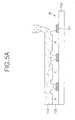
- FIGs. 5A and 5C are sectional views more specifically illustrating a formation process of the spacer-integrated planarizing layer 100.
- a liquid crystalline material-containing resin 150 is coated over the entire surface of the upper substrate 102 such that it covers the black matrix 104 and the color filter 106 and a transparent sub pixel W.
- a soft mold 152 having a groove 152a and a protrusion 150b is aligned on the resin.
- the groove 152a of the soft mold 152 corresponds to a region of the black matrix 104.
- the soft mold 152 is composed of a highly elastic rubber material, e.g., a polydimethylsiloxane (PDMS) resin, a polyurethane acrylate (PUA) resin, or a cross-linked novolac resin.
- PDMS polydimethylsiloxane
- PDA polyurethane acrylate
- the liquid crystalline material-containing resin 150 is molded in conformity with the shape of the soft mold 152 and then cured.
- the liquid crystalline material-containing resin 150 shifts into the groove 152a of the soft mold due to capillary force. Accordingly, as shown in FIG. 5C , the spacer-integrated planarizing layer 100 is formed in the pattern that is reverse-transferred to the shape of the soft mold. Since the protrusion 152b of the soft mold 152 corresponds to an effective display side at each sub pixel, the spacer-integrated planarizing layer 100 corresponding to the effective display side of the sub pixel has a flat surface.
- an alignment film is formed to cover the entire surface of the upper substrate 102, prior to coating the resin.
- the alignment film may be composed of an organic material such as polyimide.
- the present invention is applicable to vertical electric field LCD panels, where a common electrode is formed on an upper substrate, and examples of the vertical electric field LCD panels include twisted nematic (TN), electrical controlled birefringence (ECB) and vertical aligment (VA) mode LCD panels.
- TN twisted nematic
- ECB electrical controlled birefringence
- VA vertical aligment
- the common electrode is formed over the entire surface of the upper substrate 102 prior to coating the liquid crystalline material-containing resin 150.
- the common electrode may be composed of a material, e.g., indium tin oxide (ITO), tin oxide (TO), indium zinc oxide (IZO) or indium tin zinc oxide (ITZO).
- ITO indium tin oxide
- TO tin oxide
- IZO indium zinc oxide
- ITZO indium tin zinc oxide
- the liquid crystalline material-containing resin 150 comprises 30 to 40 vol% of a mono-functional monomer, 20 to 40 vol% of a di-functional monomer, 0 to 20 vol% of a tri-functional monomer, 10 vol% or more of a reactive mesogen and 1 to 3 vol% of a photoinitiator, based on a total 100 vol% of the resin.
- the reactive mesogen contains a central core with liquid-crystalline properties, a pair of photo-polymerizable end groups, and a pair of flexible spacers, each having one end bound to the central core and the other end bound to the photo-polymerizable end group.
- the central core may be selected from compounds represented by Formulae I to III below:
- the photo-polymerizable end group may be selected from (meth)acrylates, epoxides, vinyl ethers and thiol-enes.
- the flexible spacer may be selected from - (CH 2 ) x -, -O-(CH 2 ) x - (in which x is an integer of 0 to 12) and a chiral compound.
- the refractive index anisotropy of the reactive mesogen depends on the characteristics of the central core with liquid-crystalline properties.
- the reactive mesogen is preferably used in an amount of not less than 10 vol% so that it can efficiently function to compensate phase retardation values.
- the photoinitiator is a photocurable liquid polymeric precursor and is preferably contained in an amount of 1 to 3 vol%.
- the photoinitiator may be selected from aromatic ketones, phosphine oxides and di-functional initiators. More specifically, examples of suitable photoinitiators include 2-benzyl-2-(dimethylamino)-1-[4-(morpholinyl)phenyl]-1-butanone, phenyl bis(2,4,6-trimethyl benzoyl and 1-hydroxycyclohexyl phenyl ketone.
- the di-functional initiator strengthens binding between molecules, thus improving thermal properties of the reactive mesogen contained in the spacer-integrated planarizing layer 100.
- the di-functional initiator renders the optical anisotropy of the reactive mesogen to be stably maintained in a wider temperature range.
- the liquid crystalline material-containing resin 150 includes a mono-functional monomer so that it can be suitably coated.
- the resin 150 includes a tri-functional monomer as well as a di-functional monomer.
- the mono-functional monomer functions to promote the photocuring rate of the resin. To efficiently realize such a function, the mono-functional monomer is preferably in 30 to 50 vol%.
- composition of the tri- and di-functional monomers may be preferably determined, taking into the consideration the efficiency of the coating process and the light-reaction rate of the resin 150.
- the composition of the tri- and di-functional monomers is preferably determined such that the resin 150 has a viscosity equivalent to or less than 20 Cp (centi poise).
- the tri-functional monomer is preferably contained in an amount not more than 20 vol%.
- the tri- and di-functional monomers are contained in amounts of 0 to 10 vol% and 20 to 40 vol% of the total resin, respectively.
- the tri-functional monomer only can impart the desired viscosity to the resin. Since a tri-functional monomer has typically a high viscosity, a di-functional monomer may be introduced to allow the viscosity of the resin to be more readily controlled.
- Examples of the tri-functional monomer that can be used in the present invention include 1-(terahydro-4-methylenefuran-2-yl)vinyl acrylate, and 3-(2-oxooxazolidin-3-yl)buta-1,3-dien-2-yl acrylate.
- Examples of the di-functional monomer that can be used in the present invention include 1,6-hexanediol diacrylate (HDDA) and diethylene glycol dimethacrylate (DGDMA).
- the constituent components of the resin 150 are mixed in accordance with the composition as defined above to be a total 100 vol%.
- the LCD panel according to the embodiment of the present invention includes, in addition to a liquid crystalline material, the spacer-integrated planarizing layer which includes a planarized surface arranged in an effective display side at each sub pixel, and a spacer pattern that is integrated with the planarized surface and protrudes from the black matrix.
- the spacer-integrated planarizing layer 100 simultaneously functions to improve viewing angle properties of the LCD panel, planarize the sub pixel and maintain the cell gap.
- the method for fabricating the LCD panel according to the embodiment of the present invention shortens an adhesion process of a compensation film and eliminates the necessity of separately forming a planarizing layer and a spacer, thus simplifying the overall color filter array process.
Abstract
Description
- This application claims the benefit of Korean Patent Application No.
10-2007-038436, filed on April 19, 2007 - The present invention relates to a liquid crystal display panel, and more particularly, to a liquid crystal display panel and a method for fabricating the same, wherein a fabrication process of a color filter array can be simplified and an adhesion process of a compensation film can be shortened.
- Liquid crystal display devices (LCDs) control light transmittance of liquid crystal cells according to a video signal to render the liquid crystal cells to display an image corresponding to the video signal on a liquid crystal display panel arranged in the form of a matrix. In order to realize this operation, liquid crystal display devices (LCDs) include a liquid crystal display panel, where liquid crystal cells are arranged in the form of an active matrix, and driving circuits to drive the LCD panel.
- Referring to
FIG. 1 , the liquid crystal display panel includes aupper substrate 2 where a color filter array is formed, alower substrate 22 where a thinfilm transistor array 22 is formed, and aliquid crystal 11 interposed into the cell gap between theupper substrate 2 and thelower substrate 22, a lower polarizingfilm 21 adhered to a light-incident plane, a upper polarizing film 1 adhered to a light-emitting plane, and acompensation film 3 interposed between the lowerupper substrate 2 and the upper polarizing film 1. Thecompensation film 3 may be further arranged between the lower polarizingfilm 21 and thelower substrate 22. - The color filter array includes a
black matrix 4, acolor filter 6, a planarizinglayer 7 and anupper alignment layer 8 arranged on theupper substrate 2. - The thin film transistor array includes a thin film transistor (hereinafter, referred to simply as "TFT"), a
common electrode 13, apixel electrode 18 and alower alignment layer 28 arranged on thelower substrate 22. - The
upper substrate 2 and thelower substrate 22 are joined to each other such that the color filter array faces the thin film transistor array. Thespacer 10 serves to maintain the cell gap between the two substrates. - In the color filter array, the
black matrix 4 overlaps a region corresponding to the TFT of the thin film transistor array and a region corresponding to gate lines and data lines (not shown), and partitions sub pixels. Thecolor filter 6 is formed at each sub pixel partitioned by theblack matrix 4. The sub pixel includes repeated filter patterns of R, G and B sub pixels, and may further include a W sub pixel to improve brightness. Thecolor filter 6 includes R, G and B color filters, which render red, green and blue, respectively. When the sub pixel further includes a W sub pixel, thecolor filter 6 further includes a W color filter pattern at the W sub pixel. The planarizinglayer 7 is formed to cover the color filter and levels out theupper substrate 2. - In the thin film transistor array, the TFT includes a
gate electrode 12 connected to a gate line (not shown), a gateinsulating film 24, asemiconductor pattern 14 overlapping thegate electrode 12, and asource electrode 40 in ohmic contact with thesemiconductor pattern 14 and connected to the data line (not shown) that crosses the gate line, and adrain electrode 17 spaced apart from thesource electrode 40 and arranged to be in ohmic contact with thesemiconductor pattern 14. The TFT supplies a pixel signal through a data line to apixel electrode 18, in response to a scanning signal through the gate line. Thepixel electrode 18 is in contact with thedrain electrode 17 of the TFT through a contact hole in aprotective film 26. Acommon electrode 13 is formed in the form of a stripe such that it is alternately arranged with thepixel electrode 18. Thecommon electrode 13 applies a common voltage which is a base voltage of liquid crystal driving. - An
upper alignment film 8 and alower alignment film 28 render theliquid crystal 11 to be uniformly aligned. - The
liquid crystal 11 rotates in accordance with an electric field generated by the common voltage supplied from thecommon electrode 13 and the pixel voltage supplied from thepixel electrode 18 to control light-transmittance. - An upper polarizing film 1 and a lower polarizing
film 21 allow non-polarized incident lights to be linearly polarized. - Light incident to the LCD panel is linearly polarized through the lower polarizing
film 21 and is transmitted to theliquid crystal 11 having refractive index anisotropy. At the same time, the light is vertically or obliquely transmitted to theliquid crystal 11. Lights that transmit the upper polarized film in respective directions have different retardation values due to theliquid crystal 11, thus causing phase-difference. The phase-difference resulting from the transmission directions varies the properties of the transmitted lights, according to a viewing angle. Thecompensation film 3 offsets the optical phase-difference and thus improves viewing angle properties of the LCD panel. -
FIGs. 2A and2D are sectional views sequentially illustrating a method for fabricating the color filter array shown inFIG. 1 . - An opaque resin is applied over the entire surface of an
upper substrate 2 and is then patterned by photolithographic and etching processes using a first mask, to form ablack matrix 4, as shown inFIG. 2A . - A red resin is deposited on the
upper substrate 2 including theblack matrix 4 and is then patterned by photolithographic and etching processes using a second mask, to form a red color filter pattern R, as shown inFIG. 2B . In the same manner, a green, blue, and white color filter patterns G, B and W are sequentially formed using a third, fourth, and fifth mask, respectively. Green, blue and transparent resins are used to form the green, blue, and white color filter patterns G, B and W, respectively. Although no white color filter pattern W is formed, brightness can be improved. Unless there is any white color filter pattern W, theplanarizing layer 7 cannot offset the step between W sub pixels. Accordingly, it is preferable to form the white color filter pattern W, in terms of efficient planarization of the upper substrate 1, where thecolor filter 6 is formed. - An organic material is deposited over the entire surface of the
upper surface 2 including thecolor filter 6 to form aplanarizing layer 7, as shown inFIG. 2C . The planarizinglayer 7 eliminates the topology of the sub pixels which is caused by theblack matrix 2 composed of an opaque resin. - A spacer material is applied over the entire surface of the planarizing
layer 7 and is then patterned by photolithographic and etching processes using a sixth mask, to form aspacer 10, as shown inFIG. 2D . - As such, at least six mask processes are required for the fabrication of the color filter array. Each of the mask processes comprises a photolithographic process, which is a photographic process including a series of the steps of involving applying, exposing and developing a photoresist. The photolithographic process requires long process time and high equipment costs.
- The upper substrate 1 including the thin film transistor array is joined to the
lower substrate 21 including the color filter array, theliquid crystal 11 is interposed into the cell gap, and acompensation film 3 and polarizedfilms 1 and 2 are adhered. Thecompensation film 3 improves display quality of the LCD panel, but disadvantageously causing increases in material costs and fabrication process time. - Accordingly, the present invention is directed to a liquid crystal display panel and a method for fabricating the same that substantially obviate one or more problems due to limitations and disadvantages of the related art.
- An object of the present invention is to provide a liquid crystal display (LCD) panel and a method for fabricating the same, wherein a fabrication process of a color filter array can be simplified and an adhesion process of a compensation film can be shortened.
- Additional advantages, objects, and features of the invention will be set forth in part in the description which follows and in part will become apparent to those having ordinary skill in the art upon examination of the following or may be learned from practice of the invention. The objectives and other advantages of the invention may be realized and attained by the structure particularly pointed out in the written description and claims hereof as well as the appended drawings.
- To achieve these objects and other advantages and in accordance with the purpose of the invention, as embodied and broadly described herein, a liquid crystal display panel comprises: a black matrix partitioning sub pixels; a plurality of color filters formed at respective sub pixels; and a spacer-integrated planarizing layer arranged on the color filters and the black matrix, wherein the spacer-integrated planarizing layer includes a planarized surface at each of the sub pixels and a spacer pattern integrated with the planarized surface and protrudes at the black matrix, and wherein the spacer-integrated planarizing layer is composed of a liquid crystalline material to offset phase retardation difference of light.
- In another aspect of the present invention, a method for fabricating a liquid crystal display panel comprising: forming a black matrix partitioning sub pixels; forming a plurality of color filters at respective sub pixels; forming a spacer-integrated planarizing layer on the color filters and the black matrix, wherein the spacer-integrated planarizing layer includes a planarized surface at each of the sub pixels and a spacer pattern integrated with the planarized surface and protrudes at the black matrix, and wherein the spacer-integrated planarizing layer is composed of a liquid crystalline material to offset the phase retardation of light.
- The liquid crystalline material includes reactive mesogen.
- The step of forming the spacer-integrated planarizing layer includes: preparing a resin comprising 30 to 40 vol% of a mono-functional monomer, 20 to 40 vol% of a di-functional monomer, 0 to 20 vol% of a tri-functional monomer, 10 vol% or more of the reactive mesogen and 1 to 3 vol% of a photoinitiator, based on a total 100 vol% of the resin; molding the resin using a soft mold having a groove/protrusion patterns corresponding to the spacer pattern and the planarizing surface; and the photo-curing the resin.
- Each of the sub pixels includes red, green, blue and transparent sub pixels and the color filters are formed in the red, green and blue sub pixels, other than the transparent sub pixel.
- The method further comprises forming an alignment film between the color filters and the spacer-integrated planarizing layer to align the reactive mesogen.
- The method further comprises forming a common electrode between the color filters and the spacer-integrated planarizing layer.
- The method further comprises forming an alignment film between the common electrode and the spacer-integrated planarizing layer.
- It is to be understood that both the foregoing general description and the following detailed description of the present invention are exemplary and explanatory and are intended to provide further explanation of the invention as claimed.
- The accompanying drawings, which are included to provide a further understanding of the invention and are incorporated in and constitute a part of this application, illustrate embodiment(s) of the invention and together with the description serve to explain the principle of the invention. In the drawings:
-
FIG. 1 is a sectional view illustrating a conventional liquid crystal display panel; -
FIGs. 2A and2D are sectional views sequentially illustrating a process for fabricating a color filter array of a conventional liquid crystal display panel; -
FIG. 3 is a sectional view illustrating a liquid crystal display panel according to one embodiment of the present invention; -
FIG. 4A to 4C are sectional views more specifically illustrating a method for fabricating the color filter array shown inFIG. 3 ; -
FIGs. 5A to 5C are sectional views more specifically illustrating a method for fabricating an optical compensation spacer of the color filter array shown inFIG. 3 ; and -
FIG. 6 is a view illustrating one embodiment of reactive mesogen. - Reference will now be made in detail to the preferred embodiments of the present invention associated with an LCD device and a method for manufacturing the same according to the present invention, examples of which are illustrated in the annexed drawings. Wherever possible, the same reference numbers will be used throughout the drawings to refer to the same or like parts.
- Referring to
FIGs. 3 to 6 , preferred embodiments of the present invention will be described. - Referring to
FIG. 3 , the LCD panel includes aupper substrate 102 where a color filter array is formed, alower substrate 122 where a thin film transistor array is formed, and aliquid crystal 111 interposed into the cell gap between theupper substrate 102 and thelower substrate 122, a lowerpolarizing film 121 adhered to a light-incident plane, and a upperpolarizing film 101 adhered to a light-emitting plane. - The color filter array includes a
black matrix 104, acolor filter 106, a spacer-integratedplanarizing layer 100 and anupper alignment layer 108 arranged on theupper substrate 102. - The thin film transistor array includes a thin film transistor (hereinafter, referred to simply as "TFT"), a
common electrode 113, apixel electrode 118 and alower alignment layer 128 arranged on thelower substrate 122. - The
upper substrate 102 and thelower substrate 122 are joined to each other such that the color filter array faces the thin film transistor array. A cell gap is maintained by a spacer-integratedplanarizing layer 100 between the two substrates. - In the color filter array, the
black matrix 104 overlaps a region corresponding to the TFT of the thin film transistor array and a region corresponding to gate and data lines (not shown), and partitions sub pixels. Theblack matrix 104 serves to prevent leakage of lights and increase a contrast by absorbing external lights. Thecolor filter 106 is formed at each sub pixel partitioned by theblack matrix 4. The sub pixel includes R, G and B sub pixels, and may further include a W sub pixel in order to improve brightness. Thecolor filter 106 includes R, G, and B color filter patterns arranged in the R, G and B sub pixels, respectively, other than the transparent sub pixel W. The R, G, and B color filter patterns render red, green and blue, respectively. The spacer-integratedplanarizing layer 100 eliminates the topology caused by theblack matrix 104 and the W sub pixel where there is nocolor filter 106. The spacer-integratedplanarizing layer 100 is composed of a liquid crystalline material and thus offsets the phase retardation difference of light that transmit liquid crystal cells in a large viewing angle range. Similar to a bulk liquid crystal, the liquid crystalline material included in the spacer-integratedplanarizing layer 100 contains a reactive mesogen which has a constant (not variable) phase retardation value. The spacer-integratedplanarizing layer 100 includes a planarized surface in an effective display side at respective sub pixels, and a spacer pattern integrated with the planarized surface and protrudes from the boundary, i.e., theblack matrix 104, between adjacent two sub pixels. - The spacer-integrated
planarizing layer 100 acts as not only a planarizing layer to level out the sub pixel, but also as a spacer to maintain the cell gap. The planarized surface of the spacer-integratedplanarizing layer 100 enables theupper alignment film 108 to be evenly and uniformly formed on the effective display side at each sub pixel, thus rendering theliquid crystal 111 to be uniformly aligned. - The reactive mesogen has liquid crystalline properties. Accordingly, control over the refractive index anisotropy and thickness of the reactive mesogen enables control of phase retardation values. The reactive mesogen may be included in the alignment film which allows the reactive mesogen to be aligned in conformity with optical properties of the spacer-integrated
planarizing layer 100. - For example, in the case where the spacer-integrated
planarizing layer 100 has a negative C-plate property (nz<nx=ny, in which nx, ny and nz are the refractive indices in the x, y and z directions, respectively) at respective sub pixels, no further alignment film may be formed. When the reactive mesogen is not aligned with the alignment film, it is self-aligned to have the negative C-plate property. For this reason, it is unnecessary to form an additional alignment film. - As another example, in the case where the spacer-integrated
planarizing layer 100 has an A-plate property (nx>ny=nz, in which nx, ny and nz are the refractive indices in the x, y and z directions, respectively) at respective sub pixels, the reactive mesogen must be aligned in conformity with the A-plate property. Accordingly, the LCD panel according to the embodiments of the present invention includes further an alignment film to align the reactive mesogen. In such a case, the LCD panel includes further an alignment film arranged between thecolor filter 106 and the spacer-integratedplanarizing layer 100. - In the thin film transistor array, the TFT includes a
gate electrode 112 connected to a gate line (not shown), agate insulating film 124, asemiconductor pattern 114 overlapping thegate electrode 112, and asource electrode 140 in ohmic contact with thesemiconductor pattern 114 and connected to the data line (not shown) that crosses the gate line, and adrain electrode 117 spaced apart from thesource electrode 140 and arranged to be in ohmic contact with thesemiconductor pattern 114. The TFT supplies a pixel signal through a data line to apixel electrode 118, in response to a scanning signal through the gate line. Thepixel electrode 118 is in contact with thedrain electrode 117 through a contact hole in aprotective film 126. Acommon electrode 113 is formed in the form of a stripe such that it is alternatively arranged with thepixel electrode 118. Thecommon electrode 113 applies a common voltage which is a base voltage of liquid crystal driving. - An
upper alignment film 108 and alower alignment film 128 render theliquid crystal 111 to be uniformly aligned. - The
liquid crystal 111 rotates in accordance with an electric field generated by the common voltage supplied from thecommon electrode 113 and the pixel voltage supplied from thepixel electrode 118 to control light-transmittance. - An upper
polarizing film 101 and a lowerpolarizing film 121 allow non-polarized incident light to be linearly polarized. - Light incident to the LCD panel is linearly polarized through the lower
polarizing film 121 and transmitted to theliquid crystal 111 having refractive index anisotropy. At the same time, the light is vertically or obliquely transmitted to theliquid crystal 111. Lights that transmit the upper polarized film in respective directions have different retardation values by theliquid crystal 111, thus causing phase-difference. The phase retardation difference resulting from the transmission directions varies the properties of the transmitted lights according to a viewing angle. The spacer-integratedplanarizing layer 100 offsets the optical phase-difference and thus improves viewing angle properties of the LCD panel. - As mentioned above, the LCD panel according to the embodiment of the present invention includes, in addition to the liquid crystalline material, the spacer-integrated
planarizing layer 100 which includes a planarized surface arranged in an effective display side at each sub pixel, and a spacer pattern that is integrated with the planarized surface and protrudes from theblack matrix 104. The spacer-integratedplanarizing layer 100 simultaneously functions to improve viewing angle properties of the LCD panel, planarize the sub pixels and maintain the cell gap. In conclusion, the method for fabricating the LCD according to the embodiment of the present invention shortens an adhesion process of a compensation film and eliminates the necessity of separately forming a planarizing layer and a spacer, thus simplifying the overall color filter array process. -
FIGs. 4A and4C are sectional views sequentially illustrating a method for fabricating the color filter array shown inFIG. 3 . - An opaque resin is applied over the entire surface of an
upper substrate 102 and is then patterned by photolithographic and etching processes using a first mask, to form ablack matrix 104, as shown inFIG. 4A . Theblack matrix 104 may be composed of a material such as chrome (Cr). - A red resin is deposited on the
upper substrate 102 including theblack matrix 104, and is then patterned by photolithographic and etching processes using a second mask, to form a red color filter pattern R, as shown inFIG. 4B . In the same manner, green and blue color filter patterns G and B are sequentially formed using third and fourth masks, respectively. Green and blue resins are used for the green and blue color filter patterns G and B, respectively. At this time, the second and fourth mask processes are carried out by shifting the same mask. - A liquid crystalline material-containing resin is coated onto the
upper substrate 102 including thecolor filter 106. The resin is molded using a soft mold and is then photo-cured. The soft mold is separated from the cured resin, to form a spacer-integratedplanarizing layer 100, as shown inFIG. 4C . -
FIGs. 5A and5C are sectional views more specifically illustrating a formation process of the spacer-integratedplanarizing layer 100. - As shown in
FIG. 5A , a liquid crystalline material-containingresin 150 is coated over the entire surface of theupper substrate 102 such that it covers theblack matrix 104 and thecolor filter 106 and a transparent sub pixel W. - As shown in
FIG. 5B , asoft mold 152 having agroove 152a and a protrusion 150b is aligned on the resin. Thegroove 152a of thesoft mold 152 corresponds to a region of theblack matrix 104. Thesoft mold 152 is composed of a highly elastic rubber material, e.g., a polydimethylsiloxane (PDMS) resin, a polyurethane acrylate (PUA) resin, or a cross-linked novolac resin. - The liquid crystalline material-containing
resin 150 is molded in conformity with the shape of thesoft mold 152 and then cured. The liquid crystalline material-containingresin 150 shifts into thegroove 152a of the soft mold due to capillary force. Accordingly, as shown inFIG. 5C , the spacer-integratedplanarizing layer 100 is formed in the pattern that is reverse-transferred to the shape of the soft mold. Since theprotrusion 152b of thesoft mold 152 corresponds to an effective display side at each sub pixel, the spacer-integratedplanarizing layer 100 corresponding to the effective display side of the sub pixel has a flat surface. - In the case where there is a need to form an alignment film, in order to impart desirable optical properties to the liquid crystalline material contained in the liquid crystalline material-containing
resin 150, according to the method of the embodiment of the present invention, an alignment film is formed to cover the entire surface of theupper substrate 102, prior to coating the resin. The alignment film may be composed of an organic material such as polyimide. - A lateral electric field LCD panel, where a common electrode is formed on a lower substrate, has been illustrated in conjunction with
FIGs. 3 to 5c . However, the present invention is applicable to vertical electric field LCD panels, where a common electrode is formed on an upper substrate, and examples of the vertical electric field LCD panels include twisted nematic (TN), electrical controlled birefringence (ECB) and vertical aligment (VA) mode LCD panels. In the case where a vertical electric field LCD panel is formed, the common electrode is formed over the entire surface of theupper substrate 102 prior to coating the liquid crystalline material-containingresin 150. The common electrode may be composed of a material, e.g., indium tin oxide (ITO), tin oxide (TO), indium zinc oxide (IZO) or indium tin zinc oxide (ITZO). As such, in the case where a common electrode is formed on theupper substrate 102, an alignment film, to align the liquid crystalline material contained in the resin, is interposed between the liquid crystalline material-containingresin 150 and the common electrode. - The liquid crystalline material-containing
resin 150 comprises 30 to 40 vol% of a mono-functional monomer, 20 to 40 vol% of a di-functional monomer, 0 to 20 vol% of a tri-functional monomer, 10 vol% or more of a reactive mesogen and 1 to 3 vol% of a photoinitiator, based on a total 100 vol% of the resin. - As shown in
FIG. 6 , the reactive mesogen contains a central core with liquid-crystalline properties, a pair of photo-polymerizable end groups, and a pair of flexible spacers, each having one end bound to the central core and the other end bound to the photo-polymerizable end group. - In addition to the compound as shown in
FIG. 6 , the central core may be selected from compounds represented by Formulae I to III below:


- In addition to the compound as shown in
FIG. 6 , the photo-polymerizable end group may be selected from (meth)acrylates, epoxides, vinyl ethers and thiol-enes. - In addition to the compound as shown in
FIG. 6 , the flexible spacer may be selected from - (CH2)x-, -O-(CH2)x- (in which x is an integer of 0 to 12) and a chiral compound. - The refractive index anisotropy of the reactive mesogen depends on the characteristics of the central core with liquid-crystalline properties. The reactive mesogen is preferably used in an amount of not less than 10 vol% so that it can efficiently function to compensate phase retardation values.
- The photoinitiator is a photocurable liquid polymeric precursor and is preferably contained in an amount of 1 to 3 vol%. The photoinitiator may be selected from aromatic ketones, phosphine oxides and di-functional initiators. More specifically, examples of suitable photoinitiators include 2-benzyl-2-(dimethylamino)-1-[4-(morpholinyl)phenyl]-1-butanone, phenyl bis(2,4,6-trimethyl benzoyl and 1-hydroxycyclohexyl phenyl ketone.
- The di-functional initiator strengthens binding between molecules, thus improving thermal properties of the reactive mesogen contained in the spacer-integrated
planarizing layer 100. - That is, the di-functional initiator renders the optical anisotropy of the reactive mesogen to be stably maintained in a wider temperature range.
- The liquid crystalline material-containing
resin 150 includes a mono-functional monomer so that it can be suitably coated. - As the number of functional groups increase, a reaction rate may be slow. The use of a mono-functional monomer only may be considered to be advantageous in terms of process efficiency. However, in order to improve heat resistance and film properties of the
resin 150, it is necessary to introduce poly-functional groups. Thus, theresin 150 includes a tri-functional monomer as well as a di-functional monomer. - The mono-functional monomer functions to promote the photocuring rate of the resin. To efficiently realize such a function, the mono-functional monomer is preferably in 30 to 50 vol%.
- The mono-functional monomer may be selected from a vinyl monomer, CH2=CHY and CH2=CXY (in which X and Y are each independently halogen, alkyl, ester or phenyl).
- The composition of the tri- and di-functional monomers may be preferably determined, taking into the consideration the efficiency of the coating process and the light-reaction rate of the
resin 150. - In terms of the efficiency of the coating process, the composition of the tri- and di-functional monomers is preferably determined such that the
resin 150 has a viscosity equivalent to or less than 20 Cp (centi poise). In terms of the reaction rate, the tri-functional monomer is preferably contained in an amount not more than 20 vol%. - Considering the efficiency and reaction rate, the tri- and di-functional monomers are contained in amounts of 0 to 10 vol% and 20 to 40 vol% of the total resin, respectively. The tri-functional monomer only can impart the desired viscosity to the resin. Since a tri-functional monomer has typically a high viscosity, a di-functional monomer may be introduced to allow the viscosity of the resin to be more readily controlled.
- Examples of the tri-functional monomer that can be used in the present invention include 1-(terahydro-4-methylenefuran-2-yl)vinyl acrylate, and 3-(2-oxooxazolidin-3-yl)buta-1,3-dien-2-yl acrylate. Examples of the di-functional monomer that can be used in the present invention include 1,6-hexanediol diacrylate (HDDA) and diethylene glycol dimethacrylate (DGDMA).
- The constituent components of the
resin 150 are mixed in accordance with the composition as defined above to be a total 100 vol%. - As apparent from the foregoing, the LCD panel according to the embodiment of the present invention includes, in addition to a liquid crystalline material, the spacer-integrated planarizing layer which includes a planarized surface arranged in an effective display side at each sub pixel, and a spacer pattern that is integrated with the planarized surface and protrudes from the black matrix. The spacer-integrated
planarizing layer 100 simultaneously functions to improve viewing angle properties of the LCD panel, planarize the sub pixel and maintain the cell gap. In conclusion, the method for fabricating the LCD panel according to the embodiment of the present invention shortens an adhesion process of a compensation film and eliminates the necessity of separately forming a planarizing layer and a spacer, thus simplifying the overall color filter array process. - It will be apparent to those skilled in the art that various modifications and variations can be made in the present invention without departing from the spirit or scope of the inventions. Thus, it is intended that the present invention covers the modifications and variations of this invention provided they come within the scope of the appended claims and their equivalents.
Claims (17)
- A liquid crystal display panel comprising:a black matrix partitioning sub pixels;a plurality of color filters formed at respective sub pixels; anda spacer-integrated planarizing layer arranged on the color filters and the black matrix,wherein the spacer-integrated planarizing layer includes: a planarized surface at each of the sub pixels; and a spacer pattern integrated with the planarized surface and protrudes at the black matrix,
and wherein the spacer-integrated planarizing layer is composed of a liquid crystalline material to offset phase retardation difference of light. - The liquid crystal display panel according to claim 1, wherein the liquid crystalline material includes reactive mesogen.
- The liquid crystal display panel according to claim 2, further comprising:an alignment film arranged between the color filters and the spacer-integrated planarizing layer, to align the reactive mesogen.
- The liquid crystal display panel according to claim 2, wherein the reactive mesogen contains a central core with liquid-crystalline properties, and a pair of photo-polymerizable end groups bound to the central core by flexible spacers.
- The liquid crystal display panel according to claim 1, wherein each of the sub pixels includes red, green, blue and transparent sub pixels, and the color filters are formed in the red, green and blue sub pixels, other than the transparent sub pixel.
- The liquid crystal display panel according to claim 1, further comprising:an alignment film the spacer-integrated planarizing layer, to align a liquid crystal between upper and lower substrates.
- The liquid crystal display panel according to claim 1, further comprising:a common electrode arranged between the color filters and the spacer-integrated planarizing layer.
- The liquid crystal display panel according to claim 6, further comprising:an alignment film arranged between the common electrode and the spacer-integrated planarizing layer.
- A method for fabricating a liquid crystal display panel comprising:forming a black matrix partitioning sub pixels on a substrate;forming a plurality of color filters at respective sub pixels;forming a spacer-integrated planarizing layer on the color filters and the black matrix,wherein the spacer-integrated planarizing layer includes a planarized surface at each of the sub pixels and a spacer pattern integrated with the planarized surface and protrudes at the black matrix,
and wherein the spacer-integrated planarizing layer is composed of a liquid crystalline material to offset the phase retardation of light. - The method according to claim 9, wherein the liquid crystalline material includes reactive mesogen.
- The method according to claim 9, further comprising:forming an alignment film between the color filters and the spacer-integrated planarizing layer to align the reactive mesogen.
- The liquid crystal display panel according to claim 9, wherein the reactive mesogen contains a central core with liquid-crystalline properties, and a pair of photo-polymerizable end groups bound to the central core by flexible spacers.
- The method according to claim 9, wherein the step of forming the spacer-integrated planarizing layer includes:preparing a resin comprising 30 to 40 vol% of a mono-functional monomer, 20 to 40 vol% of a di-functional monomer, 0 to 20 vol% of a tri-functional monomer, 10 vol% or more of the reactive mesogen and 1 to 3 vol% of a photoinitiator, based on a total 100 vol% of the resin;molding the resin using a soft mold having groove/protrusion patterns corresponding to the spacer pattern and the planarizing surface; andthe photo curing the resin.
- The method according to claim 9, wherein each of the sub pixels includes red, green, blue and transparent sub pixels and the color filters are formed in the red, green and blue sub pixels, other than the transparent sub pixel.
- The method according to claim 9, further comprising:forming an alignment film on the spacer-integrated planarizing layer to align a liquid crystal.
- The method according to claim 9, further comprising:forming a common electrode between the color filters and the spacer-integrated planarizing layer.
- The method according to claim 16, further comprising:forming an alignment film between the common electrode and the spacer-integrated planarizing layer.
Applications Claiming Priority (1)
| Application Number | Priority Date | Filing Date | Title |
|---|---|---|---|
| KR1020070038436A KR101274048B1 (en) | 2007-04-19 | 2007-04-19 | Liquid Crystal Display Panel and Fabricating Method Thereof |
Publications (3)
| Publication Number | Publication Date |
|---|---|
| EP1986038A2 true EP1986038A2 (en) | 2008-10-29 |
| EP1986038A3 EP1986038A3 (en) | 2009-03-11 |
| EP1986038B1 EP1986038B1 (en) | 2013-02-20 |
Family
ID=39735533
Family Applications (1)
| Application Number | Title | Priority Date | Filing Date |
|---|---|---|---|
| EP07123606A Expired - Fee Related EP1986038B1 (en) | 2007-04-19 | 2007-12-19 | Liquid crystal display panel and fabricating method thereof |
Country Status (5)
| Country | Link |
|---|---|
| US (1) | US7724324B2 (en) |
| EP (1) | EP1986038B1 (en) |
| KR (1) | KR101274048B1 (en) |
| CN (1) | CN101290419B (en) |
| TW (1) | TWI365324B (en) |
Families Citing this family (21)
| Publication number | Priority date | Publication date | Assignee | Title |
|---|---|---|---|---|
| KR101329079B1 (en) | 2007-04-09 | 2013-11-20 | 엘지디스플레이 주식회사 | Liquid crystal display device and method of manufacturing the same |
| KR101490473B1 (en) * | 2008-07-01 | 2015-02-06 | 삼성디스플레이 주식회사 | Liquid crystal display including color filters |
| US8924207B2 (en) * | 2009-07-23 | 2014-12-30 | Texas Instruments Incorporated | Method and apparatus for transcoding audio data |
| CN101995687A (en) * | 2009-08-10 | 2011-03-30 | 北京京东方光电科技有限公司 | TFT-LCD panel, color film substrate and manufacturing method thereof |
| KR101675843B1 (en) * | 2010-05-04 | 2016-11-30 | 엘지디스플레이 주식회사 | Flat display device and method of fabricating the same |
| CN103038675B (en) * | 2010-07-29 | 2016-01-13 | 凸版印刷株式会社 | Color filter substrate for liquid crystal display device and liquid crystal indicator |
| CN102707564B (en) * | 2011-07-26 | 2014-04-09 | 京东方科技集团股份有限公司 | Color filter and manufacturing method thereof |
| KR101859479B1 (en) | 2011-12-06 | 2018-05-18 | 엘지디스플레이 주식회사 | Organic light emitting display device and method for fabricating the same |
| JP5921260B2 (en) * | 2012-03-02 | 2016-05-24 | スタンレー電気株式会社 | Liquid crystal display |
| JP6030315B2 (en) | 2012-03-02 | 2016-11-24 | スタンレー電気株式会社 | Liquid crystal display |
| CN202472183U (en) * | 2012-03-16 | 2012-10-03 | 京东方科技集团股份有限公司 | Transparent liquid crystal display (LCD) panel and transparent LCD |
| CN102879947B (en) * | 2012-09-27 | 2015-10-14 | 京东方科技集团股份有限公司 | Colored filter and manufacture method thereof, semitransparent semi-reflective liquid crystal display device |
| CN103364993A (en) * | 2013-03-22 | 2013-10-23 | 合肥京东方光电科技有限公司 | Liquid crystal display panel and liquid crystal display device |
| KR102122402B1 (en) * | 2013-12-31 | 2020-06-15 | 엘지디스플레이 주식회사 | COT Structure Liquid Crystal Display Device and method of fabricating the same |
| CN104035243A (en) * | 2014-06-13 | 2014-09-10 | 京东方科技集团股份有限公司 | Cushion, liquid-crystal display panel and display device |
| US20160026016A1 (en) * | 2014-07-22 | 2016-01-28 | Allen Howard Engel | Patterned layer for a liquid crystal display device that functions as an edge seal, or internal spacer, or internal gasket, or internal wall, and a precise method to manufacture the patterned layer |
| JP6698289B2 (en) | 2014-07-31 | 2020-05-27 | 三星ディスプレイ株式會社Samsung Display Co.,Ltd. | Liquid crystal display |
| KR20160028047A (en) * | 2014-09-02 | 2016-03-11 | 삼성디스플레이 주식회사 | Liquid crystal display device and manufacturing method thereof |
| CN105527755A (en) * | 2016-02-18 | 2016-04-27 | 武汉华星光电技术有限公司 | Color film substrate and liquid crystal display panel |
| US10859868B2 (en) | 2017-08-11 | 2020-12-08 | Coopervision International Limited | Flexible liquid crystal cells and lenses |
| KR102583813B1 (en) * | 2017-12-13 | 2023-09-26 | 엘지디스플레이 주식회사 | Display apparatus |
Family Cites Families (10)
| Publication number | Priority date | Publication date | Assignee | Title |
|---|---|---|---|---|
| JP3498020B2 (en) * | 1999-09-29 | 2004-02-16 | Nec液晶テクノロジー株式会社 | Active matrix substrate and manufacturing method thereof |
| GB2356462A (en) * | 1999-11-16 | 2001-05-23 | Sharp Kk | Optical properties of spacers in liquid crystal devices |
| JP2005003750A (en) * | 2003-06-10 | 2005-01-06 | Dainippon Printing Co Ltd | Phase difference control board with column |
| JP2005024920A (en) * | 2003-07-02 | 2005-01-27 | Dainippon Printing Co Ltd | Color filter substrate having phase difference control layer and its manufacturing method |
| EP1654584A1 (en) * | 2003-08-06 | 2006-05-10 | Koninklijke Philips Electronics N.V. | Stratified-phase-separated composite comprising a polymer and a liquid, and method of manufacturing the same |
| KR101007207B1 (en) * | 2003-12-27 | 2011-01-14 | 엘지디스플레이 주식회사 | Manufacturing of liquid crystal display device substrate |
| KR101086476B1 (en) * | 2004-04-14 | 2011-11-25 | 엘지디스플레이 주식회사 | Liquid Crystal Display Panel and Method of Fabricating the same |
| KR101100394B1 (en) * | 2004-09-15 | 2011-12-30 | 삼성전자주식회사 | Liquid crystal display and fabricating method the same |
| JP4344726B2 (en) * | 2004-12-30 | 2009-10-14 | エルジー ディスプレイ カンパニー リミテッド | Liquid crystal display device and manufacturing method thereof |
| KR101146524B1 (en) * | 2005-05-23 | 2012-05-25 | 엘지디스플레이 주식회사 | Liquid crystal display and method of fabricating the same |
-
2007
- 2007-04-19 KR KR1020070038436A patent/KR101274048B1/en active IP Right Grant
- 2007-12-19 EP EP07123606A patent/EP1986038B1/en not_active Expired - Fee Related
- 2007-12-26 TW TW096150386A patent/TWI365324B/en not_active IP Right Cessation
- 2007-12-28 US US12/005,629 patent/US7724324B2/en not_active Expired - Fee Related
- 2007-12-28 CN CN2007103063534A patent/CN101290419B/en not_active Expired - Fee Related
Also Published As
| Publication number | Publication date |
|---|---|
| KR101274048B1 (en) | 2013-06-12 |
| CN101290419B (en) | 2010-04-21 |
| TW200842442A (en) | 2008-11-01 |
| CN101290419A (en) | 2008-10-22 |
| EP1986038A3 (en) | 2009-03-11 |
| KR20080094259A (en) | 2008-10-23 |
| US7724324B2 (en) | 2010-05-25 |
| US20080259255A1 (en) | 2008-10-23 |
| EP1986038B1 (en) | 2013-02-20 |
| TWI365324B (en) | 2012-06-01 |
Similar Documents
| Publication | Publication Date | Title |
|---|---|---|
| EP1986038B1 (en) | Liquid crystal display panel and fabricating method thereof | |
| JP4657786B2 (en) | Liquid crystal display panel and manufacturing method thereof | |
| US7495729B2 (en) | Liquid crystal display-specific substrate having a phase difference control function, and liquid crystal display using the same | |
| US7812905B2 (en) | Liquid crystal display device and manufacturing method thereof | |
| US7436472B2 (en) | Liquid crystal display device and method with color filters having overcoat layer thereover formed on substrate except for fourth color filter formed on the overcoat layer | |
| US8477270B2 (en) | Liquid crystal display panel and method for fabricating the same | |
| JP4641162B2 (en) | Color filter with retardation layer and liquid crystal display element | |
| JP2009104182A (en) | Thin film patterning apparatus and method of fabricating color filter array substrate using the same | |
| US20080291377A1 (en) | Liquid Crystal Display Device and Manufacturing Method Thereof | |
| US10908447B2 (en) | Liquid crystal display device including liquid crystal capsule and method of fabricating the same | |
| US20220252942A1 (en) | Display panel and manufacturing method therefor, and display apparatus | |
| KR20090119450A (en) | Liquid crystal display and method for manufacturing the same | |
| US10761361B2 (en) | Liquid crystal display device including liquid crystal capsule and method of fabricating the same | |
| JP2008242001A (en) | Optical member having phase difference control function, liquid crystal device for transflective type, and manufacturing method of optical member having phase difference control function | |
| JP5150182B2 (en) | Manufacturing method of liquid crystal display device | |
| KR101225283B1 (en) | flat plate display device and the fabrication method | |
| KR101182501B1 (en) | Liquid Crystal Display device and the fabrication method thereof | |
| JP2009151267A (en) | Optical element, liquid crystal cell comprising the optical element, and manufacturing method of the optical element | |
| JP2011232537A (en) | Method of manufacturing retardation substrate, the retardation substrate, and transflective liquid crystal display apparatus | |
| JP2009265448A (en) | Color filter, and liquid crystal display device provided with color filter | |
| KR20050049651A (en) | Color filter substrate including compensation film layer and method of fabricating the same | |
| JP2013160928A (en) | Color filter for liquid crystal display, liquid crystal display device equipped with the same and manufacturing method | |
| JP2009020382A (en) | Manufacturing method of liquid crystal device and electronic apparatus |
Legal Events
| Date | Code | Title | Description |
|---|---|---|---|
| PUAI | Public reference made under article 153(3) epc to a published international application that has entered the european phase |
Free format text: ORIGINAL CODE: 0009012 |
|
| 17P | Request for examination filed |
Effective date: 20071219 |
|
| AK | Designated contracting states |
Kind code of ref document: A2 Designated state(s): AT BE BG CH CY CZ DE DK EE ES FI FR GB GR HU IE IS IT LI LT LU LV MC MT NL PL PT RO SE SI SK TR |
|
| AX | Request for extension of the european patent |
Extension state: AL BA HR MK RS |
|
| RTI1 | Title (correction) |
Free format text: LIQUID CRYSTAL DISPLAY PANEL AND FABRICATING METHOD THEREOF |
|
| PUAL | Search report despatched |
Free format text: ORIGINAL CODE: 0009013 |
|
| AK | Designated contracting states |
Kind code of ref document: A3 Designated state(s): AT BE BG CH CY CZ DE DK EE ES FI FR GB GR HU IE IS IT LI LT LU LV MC MT NL PL PT RO SE SI SK TR |
|
| AX | Request for extension of the european patent |
Extension state: AL BA HR MK RS |
|
| 17Q | First examination report despatched |
Effective date: 20090526 |
|
| R17C | First examination report despatched (corrected) |
Effective date: 20090819 |
|
| AKX | Designation fees paid |
Designated state(s): DE FR GB |
|
| GRAP | Despatch of communication of intention to grant a patent |
Free format text: ORIGINAL CODE: EPIDOSNIGR1 |
|
| GRAS | Grant fee paid |
Free format text: ORIGINAL CODE: EPIDOSNIGR3 |
|
| GRAA | (expected) grant |
Free format text: ORIGINAL CODE: 0009210 |
|
| AK | Designated contracting states |
Kind code of ref document: B1 Designated state(s): DE FR GB |
|
| REG | Reference to a national code |
Ref country code: GB Ref legal event code: FG4D |
|
| REG | Reference to a national code |
Ref country code: DE Ref legal event code: R096 Ref document number: 602007028525 Country of ref document: DE Effective date: 20130418 |
|
| PLBE | No opposition filed within time limit |
Free format text: ORIGINAL CODE: 0009261 |
|
| STAA | Information on the status of an ep patent application or granted ep patent |
Free format text: STATUS: NO OPPOSITION FILED WITHIN TIME LIMIT |
|
| 26N | No opposition filed |
Effective date: 20131121 |
|
| REG | Reference to a national code |
Ref country code: DE Ref legal event code: R097 Ref document number: 602007028525 Country of ref document: DE Effective date: 20131121 |
|
| REG | Reference to a national code |
Ref country code: FR Ref legal event code: ST Effective date: 20140829 |
|
| PG25 | Lapsed in a contracting state [announced via postgrant information from national office to epo] |
Ref country code: FR Free format text: LAPSE BECAUSE OF NON-PAYMENT OF DUE FEES Effective date: 20131231 |
|
| PGFP | Annual fee paid to national office [announced via postgrant information from national office to epo] |
Ref country code: DE Payment date: 20191021 Year of fee payment: 13 |
|
| PGFP | Annual fee paid to national office [announced via postgrant information from national office to epo] |
Ref country code: GB Payment date: 20191023 Year of fee payment: 13 |
|
| REG | Reference to a national code |
Ref country code: DE Ref legal event code: R119 Ref document number: 602007028525 Country of ref document: DE |
|
| GBPC | Gb: european patent ceased through non-payment of renewal fee |
Effective date: 20201219 |
|
| PG25 | Lapsed in a contracting state [announced via postgrant information from national office to epo] |
Ref country code: GB Free format text: LAPSE BECAUSE OF NON-PAYMENT OF DUE FEES Effective date: 20201219 Ref country code: DE Free format text: LAPSE BECAUSE OF NON-PAYMENT OF DUE FEES Effective date: 20210701 |