EP1983711A2 - Digitaler Phasenmodulator und entsprechendes Verfahren - Google Patents
Digitaler Phasenmodulator und entsprechendes Verfahren Download PDFInfo
- Publication number
- EP1983711A2 EP1983711A2 EP08103415A EP08103415A EP1983711A2 EP 1983711 A2 EP1983711 A2 EP 1983711A2 EP 08103415 A EP08103415 A EP 08103415A EP 08103415 A EP08103415 A EP 08103415A EP 1983711 A2 EP1983711 A2 EP 1983711A2
- Authority
- EP
- European Patent Office
- Prior art keywords
- counter
- signal
- input signal
- phase modulator
- value
- Prior art date
- Legal status (The legal status is an assumption and is not a legal conclusion. Google has not performed a legal analysis and makes no representation as to the accuracy of the status listed.)
- Granted
Links
Images
Classifications
-
- H—ELECTRICITY
- H04—ELECTRIC COMMUNICATION TECHNIQUE
- H04L—TRANSMISSION OF DIGITAL INFORMATION, e.g. TELEGRAPHIC COMMUNICATION
- H04L27/00—Modulated-carrier systems
- H04L27/18—Phase-modulated carrier systems, i.e. using phase-shift keying
- H04L27/20—Modulator circuits; Transmitter circuits
- H04L27/2032—Modulator circuits; Transmitter circuits for discrete phase modulation, e.g. in which the phase of the carrier is modulated in a nominally instantaneous manner
- H04L27/2092—Modulator circuits; Transmitter circuits for discrete phase modulation, e.g. in which the phase of the carrier is modulated in a nominally instantaneous manner with digital generation of the modulated carrier (does not include the modulation of a digitally generated carrier)
-
- H—ELECTRICITY
- H04—ELECTRIC COMMUNICATION TECHNIQUE
- H04R—LOUDSPEAKERS, MICROPHONES, GRAMOPHONE PICK-UPS OR LIKE ACOUSTIC ELECTROMECHANICAL TRANSDUCERS; ELECTRIC HEARING AIDS; PUBLIC ADDRESS SYSTEMS
- H04R2225/00—Details of deaf aids covered by H04R25/00, not provided for in any of its subgroups
- H04R2225/51—Aspects of antennas or their circuitry in or for hearing aids
Definitions
- the present invention relates to a digital phase modulator and a corresponding method for generating a phase-modulated signal.
- the digital phase modulator and the method for a hearing aid can be used.
- modulations of a carrier signal for example the amplitude modulation, the frequency modulation or the phase modulation, are generally carried out.
- a suitable procedure has to be chosen.
- the individual methods are usually comparatively complicated to implement in the hardware and an integration of this hardware into digital electronic components such as ASICs, FPGAs, CPLDs and the like is hardly possible.
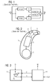
- Previous modulators usually work according to FIG. 1 with voltage controlled oscillators and several simultaneously existing phase branches. So in the example of FIG. 1 an input signal ⁇ ( t ) of the phase modulator is fed into two sub-branches. The cosine component is determined in the first branch and the sine component of the signal in the second branch. The two components are shifted in the respective branch with a desired phase ⁇ Tr t . Subsequently, they are combined in an adder to the phase-modulated signal PM.
- ⁇ Tr t an input signal ⁇ ( t ) of the phase modulator is fed into two sub-branches. The cosine component is determined in the first branch and the sine component of the signal in the second branch. The two components are shifted in the respective branch with a desired phase ⁇ Tr t . Subsequently, they are combined in an adder to the phase-modulated signal PM.
- Such a digital phase modulator is in the document EP 0 551 573 A2 described.
- hearing aids also use wireless communication. Especially in the transmission of digital signals, the phase modulation can also be advantageous here. However, since hearing aids are generally of a structurally very small design, the lines are correspondingly close together, so that the interference is more likely in conventional phase modulation methods.
- Hearing aids are portable hearing aids that are used to care for the hearing impaired.
- different types of hearing aids such as behind-the-ear hearing aids (BTE) and in-the-ear hearing aids (ITO), e.g. also Concha hearing aids or canal hearing aids (CIC), provided.
- BTE behind-the-ear hearing aids
- ITO in-the-ear hearing aids
- CIC canal hearing aids
- the hearing aids listed by way of example are worn on the outer ear or in the ear canal.
- bone conduction hearing aids, implantable or vibrotactile hearing aids are also available on the market. The stimulation of the damaged hearing takes place either mechanically or electrically.
- Hearing aids have in principle as essential components an input transducer, an amplifier and an output transducer.
- the input transducer is usually a sound receiver, z. As a microphone, and / or an electromagnetic receiver, for. B. an induction coil.
- the output transducer is usually used as an electroacoustic transducer, z. As miniature speaker, or as an electromechanical transducer, z. B. bone conduction, realized.
- the amplifier is usually integrated in a signal processing unit. This basic structure is in FIG. 1 shown using the example of a behind-the-ear hearing aid. In a hearing aid housing 1 for carrying behind the ear, one or more microphones 2 for receiving the sound from the environment are installed.
- a signal processing unit 3 which is also integrated into the hearing aid housing 1, processes the microphone signals and amplifies them she.
- the output signal of the signal processing unit 3 is transmitted to a loudspeaker or earpiece 4, which outputs an acoustic signal.
- the sound is optionally transmitted via a sound tube, which is fixed with an earmold in the ear canal, to the eardrum of the device carrier.
- the power supply of the hearing device and in particular of the signal processing unit 3 is carried out by a likewise integrated into the hearing aid housing 1 battery. 5
- the object of the present invention is to propose a phase modulator which requires the smallest possible space and which is affected as little as possible by interference.
- a corresponding method should be specified.
- a digital phase modulator having a counter for outputting a counter signal on the basis of a predetermined clock signal and a comparator containing a current counter reading from the counter for receiving a digital input signal, comparing the input signal with the current counter reading based on a predetermined assignment table and for resetting the counter when the input signal corresponds to a count assigned by the allocation table, so that a predetermined signal value of the output counter signal is phase-modulated in response to the input signal.
- Also provided by the invention is a method of generating a phase modulated digital signal by continuously incrementing / decrementing a counter based on a predetermined clock signal, assigning each of a plurality of input signal values to a counter value of the counter, comparing a current input signal value with a current counter value, and resetting the counter. when the input signal value corresponds to the associated counter value, so that a predetermined signal value of the output counter signal is phase-modulated in response to the input signal.
- the phase modulation is achieved with only one signal branch.
- the disturbances caused by one's own system are then much lower, since only one phase exists at one time and not several at the same time.
- the predetermined signal value in the digital phase modulator is the MSB (most significant bit) of the counter.
- the phase shift can then be easily fixed to the position of the MSB.
- other values of the counter can also be used for the given signal value.
- the clock signal should have at least twice the frequency of the input signal when the input signal is BPSK (Binary-Phase-Shift-Keying). If, on the other hand, QPSK modulation (Quadrature Phase Shift Keying) is to be carried out, then it is necessary for the clock signal to have at least four times the frequency of the input signal. Especially for transmission frequencies in the LW, MW and KW range such clock generators are readily available.
- the counter is clocked with a quartz oscillator. This makes very stable phase jumps achievable.
- the counter, the comparator and a transmission stage are integrated into a common logic module.
- a phase modulator with a small space and sending functionality can be realized very easily. All you have to do is connect the external antenna.
- FIG. 3 reproduced embodiment of a digital phase modulator according to the invention consists of only two essential components, a comparator 10 and a counter 11.
- the comparator 10 receives the digital data D, which are to be modulated in phase.
- the comparator 10 receives from the counter 11 a count Z.
- the data D and the count Z symbolized by an AND gate 12, compared.
- the output signal of the AND gate 12 serves as a reset signal R for synchronous resetting of the counter 11 and is supplied accordingly.
- the counter 11 is itself fed by a clock CLK having a frequency several times higher than the input signal D.
- the output signal M of the counter 11 is the corresponding phase-modulated input signal.
- FIG. 3 it may be so FIG. 3 be recognized that in the phase modulator for digital data transmission instead of multiple signal branches for signals with the respective phase positions a simple, binary counter 11 can be used. It counts, for example, for BPSK from 0 to 3 or for QPSK / BPSK from 0 to 7.
- the counter 11 is operated at a multiple of the transmission frequency, the size of the multiple depending on the desired modulation method. For low transmission frequencies in the lower megahertz range (LW, MW, KW) counters with correspondingly high clock frequencies are readily available.
- the counter 11 is reset synchronously via the comparator 10 when the comparator 10 detects one or more input data bits and the associated counter reading. If, for example, the input signal D consists of two-bit data, the phase modulation can be effected by assigning the counter value 1 to the value 00, the counter reading 3 to the value 01, the counter reading 5 to the value 11 and the counter reading 7 to the value 11.
- the counter here has eight times the clock frequency compared to the input signal. Ie. as long as a data value is present, the counter counts from 1 to 8 or from 0 to 7. If both values match, the comparator 10 outputs a reset signal R to the counter 11. The counter 11 sends out its MSB as an output signal M.
- the MSB is temporally in a fixed relationship with the reset and the resetting in turn takes place in dependence on the input data D.
- the input data D are phase-modulated output from the counter 11.
- a shift is generated in the counter 11, since it does not pass through the entire counter range depending on the input signal, but less according to the point at which the reset is triggered.
- FIG. 3 shows, can be realized in a simple manner by means of digital modules, a phase modulation.
- the counter 11 can be clocked with a quartz oscillator (CLK).
- CLK quartz oscillator
- the different phase positions do not need to be permanently available. This results in significantly less interference due to interference. In fact, only the transmission frequency with the current phase angle is generated here. Ie. Since the other phase positions are not present, there is also no interference between the phase angles.
- the phase jump is generated exactly when it is needed.
- a concrete realization may be that the comparator 10 and the counter 11 are integrated into a logic circuit, such as a CPLD, ASIC, etc.
- the output of the circuit provides the modulated transmit signal and is optionally applied to a transmit amplifier. At low transmission power can be dispensed with such an amplifier.
- an antenna can be connected directly to the logic module to realize a complete transmitter.
- a required data processing can also be accommodated in the same module.
- a single-IC transmitter can be realized by means of simple, cost-effective logic modules. If there is a logic module in the system anyway, it can be used for the transmitter including the modulator. There arises in this case, no additional circuitry, which cost-effective solutions can be realized. This is especially useful for remote controls.
Landscapes
- Engineering & Computer Science (AREA)
- Computer Networks & Wireless Communication (AREA)
- Signal Processing (AREA)
- Transmitters (AREA)
- Digital Transmission Methods That Use Modulated Carrier Waves (AREA)
Abstract
Description
- Die vorliegende Erfindung betrifft einen digitalen Phasenmodulator und ein entsprechendes Verfahren zum Erzeugen eines phasenmodulierten Signals. Insbesondere kann der digitale Phasenmodulator und das Verfahren für ein Hörgerät eingesetzt werden.
- Zur Übertragung von Daten per Funk werden in der Regel Modulationen eines Trägersignals, beispielsweise die Amplitudenmodulation, die Frequenzmodulation oder die Phasenmodulation, durchgeführt. Für jede Modulation ist ein geeignetes Verfahren zu wählen. Die einzelnen Verfahren sind in der Hardware meist vergleichsweise kompliziert zu realisieren und eine Integration dieser Hardware in digitale Elektronikbausteine wie ASICs, FPGAs, CPLDs und ähnliche ist kaum möglich.
- Bisherige Modulatoren arbeiten in der Regel gemäß
FIG 1 mit spannungsgesteuerten Oszillatoren und mehreren gleichzeitig vorhandenen Phasenzweigen. So wird in dem Beispiel vonFIG 1 ein Eingangssignal ϕ(t) des Phasenmodulators in zwei Teilzweige eingespeist. In dem ersten Zweig wird der Kosinusanteil und in dem zweiten Zweig der Sinusanteil des Signals ermittelt. Die beiden Anteile werden im jeweiligen Zweig mit einer gewünschten Phase Ω Trt verschoben. Anschließend werden sie in einem Addierer zu dem phasenmodulierten Signal PM zusammengefügt. Ein derartiger digitaler Phasenmodulator ist in der DruckschriftEP 0 551 573 A2 beschrieben. - Darüber hinaus ist aus der Patentschrift
US 4 206 423 A ebenfalls ein digitaler Phasenmodulator bekannt, bei dem alle Phasen erzeugt werden. Speziell werden zwei Phasen mit separaten Taktbausteinen generiert. Diejenige Phase, die benötigt wird, wird mithilfe einer Phasenselektorlogik ausgewählt. Bei der Realisierung eines solchen Phasenmodulators sind also viele Leitungen für Signale unterschiedlicher Phasen gleicher Frequenz zu verlegen. Die Folge sind entsprechend hohe Interferenzen. - Zunehmend wird bei Hörgeräten auch drahtlose Kommunikation eingesetzt. Speziell bei der Übertragung digitaler Signale kann auch hier die Phasenmodulation von Vorteil sein. Da jedoch Hörgeräte in der Regel baulich sehr klein ausgebildet sind, liegen die Leitungen entsprechend nahe beisammen, so dass es bei üblichen Phasenmodulationsverfahren umso mehr zu Interferenzen kommt.
- Hörgeräte sind tragbare Hörvorrichtungen, die zur Versorgung von Schwerhörenden dienen. Um den zahlreichen individuellen Bedürfnissen entgegenzukommen, werden unterschiedliche Bauformen von Hörgeräten wie Hinter-dem-Ohr-Hörgeräte (HdO) und In-dem-Ohr-Hörgeräte (IdO), z.B. auch Concha-Hörgeräte oder Kanal-Hörgeräte (CIC), bereitgestellt. Die beispielhaft aufgeführten Hörgeräte werden am Außenohr oder im Gehörgang getragen. Darüber hinaus stehen auf dem Markt aber auch Knochenleitungshörhilfen, implantierbare oder vibrotaktile Hörhilfen zur Verfügung. Dabei erfolgt die Stimulation des geschädigten Gehörs entweder mechanisch oder elektrisch.
- Hörgeräte besitzen prinzipiell als wesentliche Komponenten einen Eingangswandler, einen Verstärker und einen Ausgangswandler. Der Eingangswandler ist in der Regel ein Schallempfänger, z. B. ein Mikrofon, und/oder ein elektromagnetischer Empfänger, z. B. eine Induktionsspule. Der Ausgangswandler ist meist als elektroakustischer Wandler, z. B. Miniaturlautsprecher, oder als elektromechanischer Wandler, z. B. Knochenleitungshörer, realisiert. Der Verstärker ist üblicherweise in eine Signalverarbeitungseinheit integriert. Dieser prinzipielle Aufbau ist in
FIG 1 am Beispiel eines Hinter-dem-Ohr-Hörgeräts dargestellt. In ein Hörgerätegehäuse 1 zum Tragen hinter dem Ohr sind ein oder mehrere Mikrofone 2 zur Aufnahme des Schalls aus der Umgebung eingebaut. Eine Signalverarbeitungseinheit 3, die ebenfalls in das Hörgerätegehäuse 1 integriert ist, verarbeitet die Mikrofonsignale und verstärkt sie. Das Ausgangssignal der Signalverarbeitungseinheit 3 wird an einen Lautsprecher bzw. Hörer 4 übertragen, der ein akustisches Signal ausgibt. Der Schall wird gegebenenfalls über einen Schallschlauch, der mit einer Otoplastik im Gehörgang fixiert ist, zum Trommelfell des Geräteträgers übertragen. Die Stromversorgung des Hörgeräts und insbesondere die der Signalverarbeitungseinheit 3 erfolgt durch eine ebenfalls ins Hörgerätegehäuse 1 integrierte Batterie 5. - Die Aufgabe der vorliegenden Erfindung besteht darin, einen Phasenmodulator vorzuschlagen, der einen möglichst geringen Bauraum benötigt und der möglichst wenig durch Interferenzen beeinträchtigt ist. Außerdem soll ein entsprechendes Verfahren angegeben werden.
- Erfindungsgemäß wird diese Aufgabe gelöst durch einen digitalen Phasenmodulator mit einem Zähler zum Ausgeben eines Zählersignals auf der Basis eines vorgegebenen Taktsignals und einem Vergleicher, der von dem Zähler einen aktuellen Zählerstand enthält, zum Aufnehmen eines digitalen Eingangssignals, Vergleichen des Eingangssignals mit dem aktuellen Zählerstand anhand einer vorgegebenen Zuordnungstabelle und zum Rücksetzen des Zählers, wenn das Eingangssignal einem durch die Zuordnungstabelle zugeordneten Zählerstand entspricht, so dass ein vorgegebener Signalwert des ausgegebenen Zählersignals in Abhängigkeit von dem Eingangssignal phasenmoduliert wird.
- Außerdem wird erfindungsgemäß bereitgestellt ein Verfahren zum Erzeugen eines phasenmodulierten digitalen Signals durch kontinuierliches Hoch/Herabzählen eines Zählers auf der Basis eines vorgegebenen Taktsignals, Zuordnen jedes von mehreren Eingangssignalwerten zu einem Zählerwert des Zählers, Vergleichen eines aktuellen Eingangssignalwerts mit einem aktuellen Zählerwert und Rücksetzen des Zählers, wenn der Eingangssignalwert dem zugeordneten Zählerwert entspricht, so dass ein vorgegebener Signalwert des ausgegebenen Zählersignals in Abhängigkeit von dem Eingangssignal phasenmoduliert wird.
- In vorteilhafter Weise wird also die Phasenmodulation mit nur einem Signalzweig erreicht. Die Störungen durch das eigene System sind dann deutlich geringer, da nur eine Phasenlage zu einem Zeitpunkt existiert und nicht mehrere gleichzeitig.
- Vorzugsweise ist der vorgegebene Signalwert bei dem digitalen Phasenmodulator das MSB (most significant bit) des Zählers. Die Phasenverschiebung lässt sich dann leicht an der Position des MSB fest machen. Grundsätzlich können natürlich auch andere Werte des Zählers für den vorgegebenen Signalwert verwendet werden.
- Das Taktsignal sollte mindestens die zweifache Frequenz des Eingangssignals besitzen, wenn das Eingangssignal einer BPSK-Modulation (Binary-Phase-Shift-Keying) unterzogen wird. Soll hingegen eine QPSK-Modulation (Quadrature-Phase-Shift-Keying) durchgeführt werden, so ist es notwendig, dass das Taktsignal mindestens die vierfache Frequenz des Eingangssignals besitzt. Speziell für Sendefrequenzen im LW-, MW- und KW-Bereich sind derartige Taktgeneratoren problemlos erhältlich.
- Weiterhin ist es von Vorteil, wenn der Zähler mit einem Quarzoszillator getaktet ist. Damit sind sehr stabile Phasensprünge erreichbar.
- Entsprechend einer weiteren vorteilhaften Ausführungsform sind der Zähler, der Vergleicher und eine Sendestufe in einen gemeinsamen Logikbaustein integriert. Auf diese Weise lässt sich ein Phasenmodulator mit geringem Bauraum und Sendefunktionalität sehr einfach realisieren. Es muss nur noch die externe Antenne angeschlossen werden.
- Besonders vorteilhaft ist die Anwendung des erfindungsgemäßen digitalen Phasenmodulators bzw. des genannten erfindungsgemäßen Verfahrens bei einem Hörgerät. Hier kann man nämlich besonders von der geringen Baugröße dieses digitalen Phasenmodulators sowie den damit verbundenen verminderten Störungen profitieren. Einsetzbar ist es darüber hinaus auch bei zugehörigen Fernbedienungen.
- Die vorliegende Erfindung ist anhand der beigefügten Zeichnungen näher erläutert, in denen zeigen:
- FIG 1
- einen Schaltplan eines Phasenmodulators gemäß dem Stand der Technik;
- FIG 2
- den prinzipiellen Aufbau eines Hörgeräts gemäß dem Stand der Technik und
- FIG 3
- den prinzipiellen Aufbau eines digitalen Phasenmodulators gemäß der vorliegenden Erfindung.
- Das nachfolgend näher geschilderte Ausführungsbeispiel stellt eine bevorzugte Ausführungsform der vorliegenden Erfindung dar.
- Das in
FIG 3 wiedergegebene Ausführungsbeispiel eines erfindungsgemäßen digitalen Phasenmodulators besteht nur aus zwei wesentlichen Komponenten, einem Vergleicher 10 und einem Zähler 11. Der Vergleicher 10 nimmt die digitalen Daten D auf, die in ihrer Phase zu modulieren sind. Außerdem erhält der Vergleicher 10 von dem Zähler 11 einen Zählerstand Z. In dem Vergleicher 10 werden die Daten D und der Zählerstand Z, symbolisiert durch ein UND-Gatter 12, miteinander verglichen. Das Ausgangssignal des UND-Gatters 12 dient als Reset-Signal R zum synchronen Zurücksetzen des Zählers 11 und wird diesem entsprechend zugeleitet. - Der Zähler 11 wird selbst von einem Takt CLK, der eine mehrfach höhere Frequenz als das Eingangssignal D besitzt, gespeist. Das Ausgangssignal M des Zählers 11 ist das entsprechend phasenmodulierte Eingangssignal.
- Es kann also aus
FIG 3 erkannt werden, dass bei dem Phasenmodulator für die digitale Datenübertragung statt mehrere Signalzweige für Signale mit den jeweiligen Phasenlagen ein einfacher, binärer Zähler 11 verwendet werden kann. Er zählt beispielsweise für BPSK von 0 bis 3 bzw. für QPSK/BPSK von 0 bis 7. Der Zähler 11 wird mit einem Vielfachen der Sendefrequenz betrieben, wobei die Größe des Vielfachen von dem gewünschten Modulationsverfahrens abhängt. Für niedrige Sendefrequenzen im unteren Megahertzbereich (LW, MW, KW) sind Zähler mit entsprechend hohen Taktfrequenzen ohne weiteres erhältlich. Das Vielfache bzw. der Multiplikator gegenüber der Sendefrequenz ist beispielsweise bei BPSK-Modulation mindestens zwei und bei QPSK-Modulation mindestens vier. Der Multiplikator ergibt sich direkt aus den Phasensprüngen. Dabei gilt: Phasensprung x Multiplikator = 360°. - Der Zähler 11 wird über den Vergleicher 10 synchron zurückgesetzt, wenn der Vergleicher 10 ein oder mehrere Eingangsdatenbits und den zugehörigen Zählerstand detektiert. Besteht beispielsweise das Eingangssignal D aus Zwei-Bit-Daten, so kann die Phasenmodulation dadurch erfolgen, dass dem Wert 00 der Zählerstand 1, dem Wert 01 der Zählerstand 3, dem Wert 10 der Zählerstand 5 und dem Wert 11 der Zählerstand 7 zugeordnet wird. Der Zähler besitzt hier die achtfache Taktfrequenz gegenüber dem Eingangssignal. D. h. so lange ein Datenwert anliegt, zählt der Zähler von 1 bis 8 bzw. von 0 bis 7. Stimmen beide Werte überein, so gibt der Vergleicher 10 ein Reset-Signal R an den Zähler 11 aus. Der Zähler 11 sendet sein MSB als Ausgangssignal M aus. Das MSB steht zeitlich in einem festen Zusammenhang mit dem Rücksetzen und das Rücksetzen wiederum erfolgt in Abhängigkeit von den Eingangsdaten D. Somit werden die Eingangsdaten D phasenmoduliert von dem Zähler 11 ausgegeben. Es wird also in dem Zähler 11 eine Verschiebung erzeugt, da er je nach Eingangssignal nicht den kompletten Zählerbereich durchläuft, sondern entsprechend der Stelle, an der der Reset ausgelöst wird, weniger.
- Wie
FIG 3 zeigt, kann auf einfache Weise mittels digitaler Bausteine eine Phasenmodulation realisiert werden. Dabei kann der Zähler 11 mit einem Quarzoszillator getaktet werden (CLK). Damit ergeben sich quarzstabile Sendefrequenzen und sehr exakte Phasensprünge. Außerdem brauchen die verschiedenen Phasenlagen nicht permanent vorhanden zu sein. Hierdurch ergeben sich deutlich weniger Störsignale aufgrund von Interferenzen. Es wird hier nämlich nur die Sendefrequenz mit der gerade aktuellen Phasenlage generiert. D. h. da die anderen Phasenlagen nicht vorhanden sind, kommt es auch zu keinen Interferenzen zwischen den Phasenlagen. Der Phasensprung wird hingegen genau dann erzeugt, wenn es nötig ist. - Eine konkrete Realisierung kann darin bestehen, dass der Vergleicher 10 und der Zähler 11 in einen logischen Schaltkreis, wie einen CPLD, ASIC, etc. integriert werden. Der Ausgang der Schaltung liefert das modulierte Sendesignal und wird gegebenenfalls an einen Sendeverstärker gelegt. Bei niedrigen Sendeleistungen kann auf einen derartigen Verstärker verzichtet werden. In diesem Fall kann eine Antenne direkt an den Logikbaustein angeschlossen werden, um einen vollständigen Sender zu realisieren.
- Optional kann eine erforderliche Datenverarbeitung ebenfalls in dem gleichen Baustein untergebracht werden. Somit lässt sich ein Ein-IC-Sender mittels einfacher, kostengünstiger Logikbausteine realisieren. Wenn ohnehin ein Logikbaustein im System vorhanden ist, kann dieser für den Sender inklusiv Modulator mit verwendet werden. Es entsteht in diesem Fall kein zusätzlicher Schaltungsaufwand, wodurch kostengünstige Lösungen realisierbar sind. Das ist speziell für Fernbedienungen von Vorteil.
Claims (12)
- Digitaler Phasenmodulator mit- einem Zähler (11) zum Ausgeben eines Zählersignals (M) auf der Basis eines vorgegebenen Taktsignals (CLK) und- einem Vergleicher (10), der von dem Zähler einen aktuellen Zählerstand (Z) enthält, zum Aufnehmen eines digitalen Eingangssignals (D), Vergleichen des Eingangssignals (D) mit dem aktuellen Zählerstand (Z) anhand einer vorgegebenen Zuordnungstabelle und zum Rücksetzen des Zählers (11), wenn das Eingangssignal (D) einem durch die Zuordnungstabelle zugeordneten Zählerstand entspricht, so dass- ein vorgegebener Signalwert des ausgegebenen Zählersignals (M) in Abhängigkeit von dem Eingangssignal (D) phasenmoduliert wird.
- Digitaler Phasenmodulator nach Anspruch 1, wobei der vorgegebene Signalwert das MSB des Zählers (11) ist.
- Digitaler Phasenmodulator nach Anspruch 1 oder 2, wobei das Taktsignal (CLK) mindestens die zweifache Frequenz des Eingangssignals (D) besitzt, und das Eingangssignal (D) durch den Zähler (11) einer BPSK-Modulation unterzogen wird.
- Digitaler Phasenmodulator nach Anspruch 1 oder 2, wobei das Taktsignal (CLK) mindestens die vierfache Frequenz des Eingangssignals (D) besitzt, und das Eingangssignal (D) durch den Zähler (11) einer QPSK-Modulation unterzogen wird.
- Digitaler Phasenmodulator nach einem der vorhergehenden Ansprüche, wobei der Zähler (11) mit einem Quarzoszillator getaktet ist.
- Digitaler Phasenmodulator nach einem der vorhergehenden Ansprüche, wobei der Zähler (11), der Vergleicher (10) und eine Sendestufe in einen gemeinsamen Logikbaustein integriert sind.
- Verfahren zum Erzeugen eines phasenmodulierten digitalen Signals durch- kontinuierliches Hoch/Herabzählen eines Zählers (11) auf der Basis eines vorgegebenen Taktsignals (CLK),- Zuordnen jedes von mehreren Eingangssignalwerten zu einem Zählerwert des Zählers (11),- Vergleichen eines aktuellen Eingangssignalwerts mit einem aktuellen Zählerwert und- Rücksetzen des Zählers (11), wenn der Eingangssignalwert dem zugeordneten Zählerwert entspricht, so dass- ein vorgegebener Signalwert des ausgegebenen Zählersignals (M) in Abhängigkeit von dem Eingangssignal phasenmoduliert wird.
- Verfahren nach Anspruch 7, wobei der vorgegebene Signalwert das MSB des Zählers (11) ist.
- Verfahren nach Anspruch 7 oder 8, wobei das Taktsignal (CLK) mindestens die zweifache Frequenz des Eingangssignals besitzt, und das Eingangssignal (D) durch den Zähler (11) einer BPSK-Modulation unterzogen wird.
- Verfahren nach Anspruch 7 oder 8, wobei das Taktsignal (CLK) mindestens die vierfache Frequenz des Eingangssignals besitzt, und das Eingangssignal (D) durch den Zähler (11) einer QPSK-Modulation unterzogen wird.
- Hörgerät mit einem digitalen Phasenmodulator nach einem der Ansprüche 1 bis 6.
- Fernbedienung mit einem digitalen Phasenmodulator nach einem der Ansprüche 1 bis 6.
Applications Claiming Priority (1)
| Application Number | Priority Date | Filing Date | Title |
|---|---|---|---|
| DE102007018087 | 2007-04-17 |
Publications (3)
| Publication Number | Publication Date |
|---|---|
| EP1983711A2 true EP1983711A2 (de) | 2008-10-22 |
| EP1983711A3 EP1983711A3 (de) | 2014-08-06 |
| EP1983711B1 EP1983711B1 (de) | 2019-06-12 |
Family
ID=39672026
Family Applications (1)
| Application Number | Title | Priority Date | Filing Date |
|---|---|---|---|
| EP08103415.9A Active EP1983711B1 (de) | 2007-04-17 | 2008-04-07 | Digitaler Phasenmodulator und entsprechendes Verfahren |
Country Status (3)
| Country | Link |
|---|---|
| US (1) | US7737799B2 (de) |
| EP (1) | EP1983711B1 (de) |
| DK (1) | DK1983711T3 (de) |
Citations (2)
| Publication number | Priority date | Publication date | Assignee | Title |
|---|---|---|---|---|
| US4206423A (en) | 1978-10-03 | 1980-06-03 | Rca Corporation | Digitized phase modulating means |
| EP0551573A2 (de) | 1992-01-15 | 1993-07-21 | Robert Bosch Gmbh | Winkelmodulator, insbesondere für digitale Funkübertragung |
Family Cites Families (7)
| Publication number | Priority date | Publication date | Assignee | Title |
|---|---|---|---|---|
| US3781706A (en) * | 1972-08-04 | 1973-12-25 | Us Navy | Incremental phase shift frequency synthesizer |
| US4562415A (en) * | 1984-06-22 | 1985-12-31 | Motorola, Inc. | Universal ultra-precision PSK modulator with time multiplexed modes of varying modulation types |
| US4794621A (en) * | 1987-08-26 | 1988-12-27 | Josef Dirr | Apparatus for transmitting information by angle modulation |
| DE3919530A1 (de) * | 1989-06-15 | 1990-12-20 | Ant Nachrichtentech | Verfahren zur digitalen modulation und digitaler modulator |
| US5627500A (en) * | 1995-12-26 | 1997-05-06 | Tektronix, Inc. | Phase modulator having individually placed edges |
| US6791596B2 (en) * | 2001-06-28 | 2004-09-14 | Ricoh Company, Ltd. | Method and apparatus for image forming capable of effectively generating pixel clock pulses |
| DE102004062364A1 (de) * | 2004-12-13 | 2006-06-14 | Atmel Germany Gmbh | Verfahren zur drahtlosen Datenübertragung |
-
2008
- 2008-04-07 EP EP08103415.9A patent/EP1983711B1/de active Active
- 2008-04-07 DK DK08103415.9T patent/DK1983711T3/da active
- 2008-04-16 US US12/148,118 patent/US7737799B2/en active Active
Patent Citations (2)
| Publication number | Priority date | Publication date | Assignee | Title |
|---|---|---|---|---|
| US4206423A (en) | 1978-10-03 | 1980-06-03 | Rca Corporation | Digitized phase modulating means |
| EP0551573A2 (de) | 1992-01-15 | 1993-07-21 | Robert Bosch Gmbh | Winkelmodulator, insbesondere für digitale Funkübertragung |
Also Published As
| Publication number | Publication date |
|---|---|
| DK1983711T3 (da) | 2019-09-23 |
| US7737799B2 (en) | 2010-06-15 |
| US20080258832A1 (en) | 2008-10-23 |
| EP1983711A3 (de) | 2014-08-06 |
| EP1983711B1 (de) | 2019-06-12 |
Similar Documents
| Publication | Publication Date | Title |
|---|---|---|
| EP1962557B1 (de) | Hörvorrichtung mit einem speziellen Energieaufnahmesystem und entsprechendes Verfahren | |
| EP1915031A2 (de) | Hörsystem mit Fernbedienung als Basisstation und entsprechendes Kommunikationsverfahren | |
| EP2437258B1 (de) | Verfahren und Vorrichtung zur Frequenzkompression mit selektiver Frequenzverschiebung | |
| EP2053876A1 (de) | Hörvorrichtung mit gemeinsamem Anschluss für Schirmung und Identifikation eines Hörers | |
| DE60002491T2 (de) | Burst-leistungsverstärker mit individuellen rampenprofilen in abhängigkeit des ersten nachrichtensymbols | |
| EP2899845A1 (de) | Ladegerät mit dualem Antennensystem und Verfahren zum drahtlosen Laden eines oder mehrerer Hörgeräte | |
| DE102011006471A1 (de) | Hörhilfegerät mit einem Richtmikrofonsystem sowie Verfahren zum Einstellen eines Richtmikrofons bei einem Hörhilfegerät | |
| CH673551A5 (en) | Hearing aid with direct audio input connection - provided by audio plug fitted into battery compartment upon battery removal | |
| EP2104377A2 (de) | Hörsystem mit Teilbandsignalaustausch und entsprechendes Verfahren | |
| DE19947019A1 (de) | Verfahren und Vorrichtung zum Erzeugen von spreizcodierten Signalen | |
| DE102016222323A1 (de) | Hörhilfegerät mit Elektronikrahmen und darin integrierter Antenne | |
| EP1959712A2 (de) | Hörvorrichtung mit Hörerkompensationsspule | |
| EP2811762A1 (de) | Logik-basiertes binaurales Beam-Formungssystem | |
| DE102007018121B4 (de) | Hörvorrichtung mit störarmer Höreransteuerung und entsprechendes Verfahren sowie Hörsystem | |
| EP4033782B1 (de) | Hörgerät | |
| EP1983711B1 (de) | Digitaler Phasenmodulator und entsprechendes Verfahren | |
| DE102009058415B4 (de) | Verfahren zur Frequenztransposition bei einem Hörhilfegerät sowie Hörhilfegerät | |
| EP2822300A1 (de) | Erkennen von Hörsituationen mit unterschiedlichen Signalquellen | |
| EP2437521B1 (de) | Verfahren zur Frequenzkompression mit harmonischer Korrektur und entsprechende Vorrichtung | |
| EP3742759A1 (de) | Hörgerät sowie verfahren zum betrieb eines hörgerätes | |
| DE102007054603B4 (de) | Hörvorrichtung mit gesteuerter Programmierbuchse | |
| EP3396979A1 (de) | Verfahren zur herstellung eines tragrahmens eines hörhilfegeräts und tragrahmen sowie hörhilfegerät | |
| EP2418876A1 (de) | Verfahren zum Reduzieren von Interferenzen und Hörvorrichtung | |
| EP2362687A2 (de) | Hörvorrichtung mit parallel betriebenen Rückkopplungsreduktionsfiltern und Verfahren | |
| EP1915030A1 (de) | Hörgerät mit stromführendem Metallbügel |
Legal Events
| Date | Code | Title | Description |
|---|---|---|---|
| PUAI | Public reference made under article 153(3) epc to a published international application that has entered the european phase |
Free format text: ORIGINAL CODE: 0009012 |
|
| AK | Designated contracting states |
Kind code of ref document: A2 Designated state(s): AT BE BG CH CY CZ DE DK EE ES FI FR GB GR HR HU IE IS IT LI LT LU LV MC MT NL NO PL PT RO SE SI SK TR |
|
| AX | Request for extension of the european patent |
Extension state: AL BA MK RS |
|
| PUAL | Search report despatched |
Free format text: ORIGINAL CODE: 0009013 |
|
| AK | Designated contracting states |
Kind code of ref document: A3 Designated state(s): AT BE BG CH CY CZ DE DK EE ES FI FR GB GR HR HU IE IS IT LI LT LU LV MC MT NL NO PL PT RO SE SI SK TR |
|
| AX | Request for extension of the european patent |
Extension state: AL BA MK RS |
|
| RIC1 | Information provided on ipc code assigned before grant |
Ipc: H04L 27/20 20060101AFI20140629BHEP |
|
| 17P | Request for examination filed |
Effective date: 20150203 |
|
| RBV | Designated contracting states (corrected) |
Designated state(s): AT BE BG CH CY CZ DE DK EE ES FI FR GB GR HR HU IE IS IT LI LT LU LV MC MT NL NO PL PT RO SE SI SK TR |
|
| AKX | Designation fees paid |
Designated state(s): AT BE BG CH CY CZ DE DK EE ES FI FR GB GR HR HU IE IS IT LI LT LU LV MC MT NL NO PL PT RO SE SI SK TR |
|
| AXX | Extension fees paid |
Extension state: RS Extension state: MK Extension state: BA Extension state: AL |
|
| RAP1 | Party data changed (applicant data changed or rights of an application transferred) |
Owner name: SIVANTOS GMBH |
|
| STAA | Information on the status of an ep patent application or granted ep patent |
Free format text: STATUS: EXAMINATION IS IN PROGRESS |
|
| 17Q | First examination report despatched |
Effective date: 20180209 |
|
| GRAP | Despatch of communication of intention to grant a patent |
Free format text: ORIGINAL CODE: EPIDOSNIGR1 |
|
| STAA | Information on the status of an ep patent application or granted ep patent |
Free format text: STATUS: GRANT OF PATENT IS INTENDED |
|
| INTG | Intention to grant announced |
Effective date: 20190110 |
|
| GRAS | Grant fee paid |
Free format text: ORIGINAL CODE: EPIDOSNIGR3 |
|
| GRAA | (expected) grant |
Free format text: ORIGINAL CODE: 0009210 |
|
| STAA | Information on the status of an ep patent application or granted ep patent |
Free format text: STATUS: THE PATENT HAS BEEN GRANTED |
|
| AK | Designated contracting states |
Kind code of ref document: B1 Designated state(s): AT BE BG CH CY CZ DE DK EE ES FI FR GB GR HR HU IE IS IT LI LT LU LV MC MT NL NO PL PT RO SE SI SK TR |
|
| REG | Reference to a national code |
Ref country code: GB Ref legal event code: FG4D Free format text: NOT ENGLISH |
|
| REG | Reference to a national code |
Ref country code: CH Ref legal event code: EP |
|
| REG | Reference to a national code |
Ref country code: AT Ref legal event code: REF Ref document number: 1144034 Country of ref document: AT Kind code of ref document: T Effective date: 20190615 |
|
| REG | Reference to a national code |
Ref country code: DE Ref legal event code: R096 Ref document number: 502008016804 Country of ref document: DE |
|
| REG | Reference to a national code |
Ref country code: IE Ref legal event code: FG4D Free format text: LANGUAGE OF EP DOCUMENT: GERMAN |
|
| REG | Reference to a national code |
Ref country code: CH Ref legal event code: NV Representative=s name: E. BLUM AND CO. AG PATENT- UND MARKENANWAELTE , CH |
|
| REG | Reference to a national code |
Ref country code: DK Ref legal event code: T3 Effective date: 20190916 |
|
| REG | Reference to a national code |
Ref country code: NL Ref legal event code: MP Effective date: 20190612 |
|
| REG | Reference to a national code |
Ref country code: LT Ref legal event code: MG4D |
|
| PG25 | Lapsed in a contracting state [announced via postgrant information from national office to epo] |
Ref country code: HR Free format text: LAPSE BECAUSE OF FAILURE TO SUBMIT A TRANSLATION OF THE DESCRIPTION OR TO PAY THE FEE WITHIN THE PRESCRIBED TIME-LIMIT Effective date: 20190612 Ref country code: NO Free format text: LAPSE BECAUSE OF FAILURE TO SUBMIT A TRANSLATION OF THE DESCRIPTION OR TO PAY THE FEE WITHIN THE PRESCRIBED TIME-LIMIT Effective date: 20190912 Ref country code: ES Free format text: LAPSE BECAUSE OF FAILURE TO SUBMIT A TRANSLATION OF THE DESCRIPTION OR TO PAY THE FEE WITHIN THE PRESCRIBED TIME-LIMIT Effective date: 20190612 Ref country code: LT Free format text: LAPSE BECAUSE OF FAILURE TO SUBMIT A TRANSLATION OF THE DESCRIPTION OR TO PAY THE FEE WITHIN THE PRESCRIBED TIME-LIMIT Effective date: 20190612 Ref country code: SE Free format text: LAPSE BECAUSE OF FAILURE TO SUBMIT A TRANSLATION OF THE DESCRIPTION OR TO PAY THE FEE WITHIN THE PRESCRIBED TIME-LIMIT Effective date: 20190612 Ref country code: FI Free format text: LAPSE BECAUSE OF FAILURE TO SUBMIT A TRANSLATION OF THE DESCRIPTION OR TO PAY THE FEE WITHIN THE PRESCRIBED TIME-LIMIT Effective date: 20190612 |
|
| PG25 | Lapsed in a contracting state [announced via postgrant information from national office to epo] |
Ref country code: BG Free format text: LAPSE BECAUSE OF FAILURE TO SUBMIT A TRANSLATION OF THE DESCRIPTION OR TO PAY THE FEE WITHIN THE PRESCRIBED TIME-LIMIT Effective date: 20190912 Ref country code: GR Free format text: LAPSE BECAUSE OF FAILURE TO SUBMIT A TRANSLATION OF THE DESCRIPTION OR TO PAY THE FEE WITHIN THE PRESCRIBED TIME-LIMIT Effective date: 20190913 Ref country code: LV Free format text: LAPSE BECAUSE OF FAILURE TO SUBMIT A TRANSLATION OF THE DESCRIPTION OR TO PAY THE FEE WITHIN THE PRESCRIBED TIME-LIMIT Effective date: 20190612 |
|
| PG25 | Lapsed in a contracting state [announced via postgrant information from national office to epo] |
Ref country code: SK Free format text: LAPSE BECAUSE OF FAILURE TO SUBMIT A TRANSLATION OF THE DESCRIPTION OR TO PAY THE FEE WITHIN THE PRESCRIBED TIME-LIMIT Effective date: 20190612 Ref country code: RO Free format text: LAPSE BECAUSE OF FAILURE TO SUBMIT A TRANSLATION OF THE DESCRIPTION OR TO PAY THE FEE WITHIN THE PRESCRIBED TIME-LIMIT Effective date: 20190612 Ref country code: CZ Free format text: LAPSE BECAUSE OF FAILURE TO SUBMIT A TRANSLATION OF THE DESCRIPTION OR TO PAY THE FEE WITHIN THE PRESCRIBED TIME-LIMIT Effective date: 20190612 Ref country code: PT Free format text: LAPSE BECAUSE OF FAILURE TO SUBMIT A TRANSLATION OF THE DESCRIPTION OR TO PAY THE FEE WITHIN THE PRESCRIBED TIME-LIMIT Effective date: 20191014 Ref country code: NL Free format text: LAPSE BECAUSE OF FAILURE TO SUBMIT A TRANSLATION OF THE DESCRIPTION OR TO PAY THE FEE WITHIN THE PRESCRIBED TIME-LIMIT Effective date: 20190612 Ref country code: EE Free format text: LAPSE BECAUSE OF FAILURE TO SUBMIT A TRANSLATION OF THE DESCRIPTION OR TO PAY THE FEE WITHIN THE PRESCRIBED TIME-LIMIT Effective date: 20190612 |
|
| PG25 | Lapsed in a contracting state [announced via postgrant information from national office to epo] |
Ref country code: IS Free format text: LAPSE BECAUSE OF FAILURE TO SUBMIT A TRANSLATION OF THE DESCRIPTION OR TO PAY THE FEE WITHIN THE PRESCRIBED TIME-LIMIT Effective date: 20191012 Ref country code: IT Free format text: LAPSE BECAUSE OF FAILURE TO SUBMIT A TRANSLATION OF THE DESCRIPTION OR TO PAY THE FEE WITHIN THE PRESCRIBED TIME-LIMIT Effective date: 20190612 |
|
| REG | Reference to a national code |
Ref country code: DE Ref legal event code: R097 Ref document number: 502008016804 Country of ref document: DE |
|
| PG25 | Lapsed in a contracting state [announced via postgrant information from national office to epo] |
Ref country code: TR Free format text: LAPSE BECAUSE OF FAILURE TO SUBMIT A TRANSLATION OF THE DESCRIPTION OR TO PAY THE FEE WITHIN THE PRESCRIBED TIME-LIMIT Effective date: 20190612 |
|
| PLBE | No opposition filed within time limit |
Free format text: ORIGINAL CODE: 0009261 |
|
| STAA | Information on the status of an ep patent application or granted ep patent |
Free format text: STATUS: NO OPPOSITION FILED WITHIN TIME LIMIT |
|
| PG25 | Lapsed in a contracting state [announced via postgrant information from national office to epo] |
Ref country code: PL Free format text: LAPSE BECAUSE OF FAILURE TO SUBMIT A TRANSLATION OF THE DESCRIPTION OR TO PAY THE FEE WITHIN THE PRESCRIBED TIME-LIMIT Effective date: 20190612 |
|
| 26N | No opposition filed |
Effective date: 20200313 |
|
| PG25 | Lapsed in a contracting state [announced via postgrant information from national office to epo] |
Ref country code: SI Free format text: LAPSE BECAUSE OF FAILURE TO SUBMIT A TRANSLATION OF THE DESCRIPTION OR TO PAY THE FEE WITHIN THE PRESCRIBED TIME-LIMIT Effective date: 20190612 Ref country code: IS Free format text: LAPSE BECAUSE OF FAILURE TO SUBMIT A TRANSLATION OF THE DESCRIPTION OR TO PAY THE FEE WITHIN THE PRESCRIBED TIME-LIMIT Effective date: 20200224 |
|
| PG2D | Information on lapse in contracting state deleted |
Ref country code: IS |
|
| PG25 | Lapsed in a contracting state [announced via postgrant information from national office to epo] |
Ref country code: IS Free format text: LAPSE BECAUSE OF FAILURE TO SUBMIT A TRANSLATION OF THE DESCRIPTION OR TO PAY THE FEE WITHIN THE PRESCRIBED TIME-LIMIT Effective date: 20191112 |
|
| PG25 | Lapsed in a contracting state [announced via postgrant information from national office to epo] |
Ref country code: MC Free format text: LAPSE BECAUSE OF FAILURE TO SUBMIT A TRANSLATION OF THE DESCRIPTION OR TO PAY THE FEE WITHIN THE PRESCRIBED TIME-LIMIT Effective date: 20190612 |
|
| PG25 | Lapsed in a contracting state [announced via postgrant information from national office to epo] |
Ref country code: LU Free format text: LAPSE BECAUSE OF NON-PAYMENT OF DUE FEES Effective date: 20200407 |
|
| REG | Reference to a national code |
Ref country code: BE Ref legal event code: MM Effective date: 20200430 |
|
| PG25 | Lapsed in a contracting state [announced via postgrant information from national office to epo] |
Ref country code: BE Free format text: LAPSE BECAUSE OF NON-PAYMENT OF DUE FEES Effective date: 20200430 |
|
| PG25 | Lapsed in a contracting state [announced via postgrant information from national office to epo] |
Ref country code: IE Free format text: LAPSE BECAUSE OF NON-PAYMENT OF DUE FEES Effective date: 20200407 |
|
| REG | Reference to a national code |
Ref country code: AT Ref legal event code: MM01 Ref document number: 1144034 Country of ref document: AT Kind code of ref document: T Effective date: 20200407 |
|
| PG25 | Lapsed in a contracting state [announced via postgrant information from national office to epo] |
Ref country code: AT Free format text: LAPSE BECAUSE OF NON-PAYMENT OF DUE FEES Effective date: 20200407 |
|
| PG25 | Lapsed in a contracting state [announced via postgrant information from national office to epo] |
Ref country code: MT Free format text: LAPSE BECAUSE OF FAILURE TO SUBMIT A TRANSLATION OF THE DESCRIPTION OR TO PAY THE FEE WITHIN THE PRESCRIBED TIME-LIMIT Effective date: 20190612 Ref country code: CY Free format text: LAPSE BECAUSE OF FAILURE TO SUBMIT A TRANSLATION OF THE DESCRIPTION OR TO PAY THE FEE WITHIN THE PRESCRIBED TIME-LIMIT Effective date: 20190612 |
|
| PGFP | Annual fee paid to national office [announced via postgrant information from national office to epo] |
Ref country code: GB Payment date: 20240423 Year of fee payment: 17 |
|
| PGFP | Annual fee paid to national office [announced via postgrant information from national office to epo] |
Ref country code: DE Payment date: 20240418 Year of fee payment: 17 |
|
| PGFP | Annual fee paid to national office [announced via postgrant information from national office to epo] |
Ref country code: DK Payment date: 20240422 Year of fee payment: 17 |
|
| PGFP | Annual fee paid to national office [announced via postgrant information from national office to epo] |
Ref country code: CH Payment date: 20240501 Year of fee payment: 17 |
|
| PGFP | Annual fee paid to national office [announced via postgrant information from national office to epo] |
Ref country code: FR Payment date: 20240419 Year of fee payment: 17 |
|
| REG | Reference to a national code |
Ref country code: DE Ref legal event code: R119 Ref document number: 502008016804 Country of ref document: DE |
|
| REG | Reference to a national code |
Ref country code: DK Ref legal event code: EBP Effective date: 20250430 |
|
| REG | Reference to a national code |
Ref country code: CH Ref legal event code: H13 Free format text: ST27 STATUS EVENT CODE: U-0-0-H10-H13 (AS PROVIDED BY THE NATIONAL OFFICE) Effective date: 20251125 |
|
| GBPC | Gb: european patent ceased through non-payment of renewal fee |
Effective date: 20250407 |
|
| PG25 | Lapsed in a contracting state [announced via postgrant information from national office to epo] |
Ref country code: DE Free format text: LAPSE BECAUSE OF NON-PAYMENT OF DUE FEES Effective date: 20251104 |
|
| PG25 | Lapsed in a contracting state [announced via postgrant information from national office to epo] |
Ref country code: GB Free format text: LAPSE BECAUSE OF NON-PAYMENT OF DUE FEES Effective date: 20250407 |
|
| PG25 | Lapsed in a contracting state [announced via postgrant information from national office to epo] |
Ref country code: FR Free format text: LAPSE BECAUSE OF NON-PAYMENT OF DUE FEES Effective date: 20250430 |
|
| PG25 | Lapsed in a contracting state [announced via postgrant information from national office to epo] |
Ref country code: CH Free format text: LAPSE BECAUSE OF NON-PAYMENT OF DUE FEES Effective date: 20250430 |
|
| PG25 | Lapsed in a contracting state [announced via postgrant information from national office to epo] |
Ref country code: DK Free format text: LAPSE BECAUSE OF NON-PAYMENT OF DUE FEES Effective date: 20250430 |