EP1983579A2 - Method of manufacturing semiconductor film and method of manufacturing photovoltaic element - Google Patents
Method of manufacturing semiconductor film and method of manufacturing photovoltaic element Download PDFInfo
- Publication number
- EP1983579A2 EP1983579A2 EP08251466A EP08251466A EP1983579A2 EP 1983579 A2 EP1983579 A2 EP 1983579A2 EP 08251466 A EP08251466 A EP 08251466A EP 08251466 A EP08251466 A EP 08251466A EP 1983579 A2 EP1983579 A2 EP 1983579A2
- Authority
- EP
- European Patent Office
- Prior art keywords
- source gas
- semiconductor film
- manufacturing
- catalytic wire
- photovoltaic element
- Prior art date
- Legal status (The legal status is an assumption and is not a legal conclusion. Google has not performed a legal analysis and makes no representation as to the accuracy of the status listed.)
- Ceased
Links
Images

Classifications
-
- H—ELECTRICITY
- H10—SEMICONDUCTOR DEVICES; ELECTRIC SOLID-STATE DEVICES NOT OTHERWISE PROVIDED FOR
- H10F—INORGANIC SEMICONDUCTOR DEVICES SENSITIVE TO INFRARED RADIATION, LIGHT, ELECTROMAGNETIC RADIATION OF SHORTER WAVELENGTH OR CORPUSCULAR RADIATION
- H10F71/00—Manufacture or treatment of devices covered by this subclass
- H10F71/10—Manufacture or treatment of devices covered by this subclass the devices comprising amorphous semiconductor material
- H10F71/103—Manufacture or treatment of devices covered by this subclass the devices comprising amorphous semiconductor material including only Group IV materials
-
- H—ELECTRICITY
- H10—SEMICONDUCTOR DEVICES; ELECTRIC SOLID-STATE DEVICES NOT OTHERWISE PROVIDED FOR
- H10P—GENERIC PROCESSES OR APPARATUS FOR THE MANUFACTURE OR TREATMENT OF DEVICES COVERED BY CLASS H10
- H10P14/00—Formation of materials, e.g. in the shape of layers or pillars
- H10P14/20—Formation of materials, e.g. in the shape of layers or pillars of semiconductor materials
-
- C—CHEMISTRY; METALLURGY
- C23—COATING METALLIC MATERIAL; COATING MATERIAL WITH METALLIC MATERIAL; CHEMICAL SURFACE TREATMENT; DIFFUSION TREATMENT OF METALLIC MATERIAL; COATING BY VACUUM EVAPORATION, BY SPUTTERING, BY ION IMPLANTATION OR BY CHEMICAL VAPOUR DEPOSITION, IN GENERAL; INHIBITING CORROSION OF METALLIC MATERIAL OR INCRUSTATION IN GENERAL
- C23C—COATING METALLIC MATERIAL; COATING MATERIAL WITH METALLIC MATERIAL; SURFACE TREATMENT OF METALLIC MATERIAL BY DIFFUSION INTO THE SURFACE, BY CHEMICAL CONVERSION OR SUBSTITUTION; COATING BY VACUUM EVAPORATION, BY SPUTTERING, BY ION IMPLANTATION OR BY CHEMICAL VAPOUR DEPOSITION, IN GENERAL
- C23C16/00—Chemical coating by decomposition of gaseous compounds, without leaving reaction products of surface material in the coating, i.e. chemical vapour deposition [CVD] processes
- C23C16/22—Chemical coating by decomposition of gaseous compounds, without leaving reaction products of surface material in the coating, i.e. chemical vapour deposition [CVD] processes characterised by the deposition of inorganic material, other than metallic material
- C23C16/24—Deposition of silicon only
-
- C—CHEMISTRY; METALLURGY
- C23—COATING METALLIC MATERIAL; COATING MATERIAL WITH METALLIC MATERIAL; CHEMICAL SURFACE TREATMENT; DIFFUSION TREATMENT OF METALLIC MATERIAL; COATING BY VACUUM EVAPORATION, BY SPUTTERING, BY ION IMPLANTATION OR BY CHEMICAL VAPOUR DEPOSITION, IN GENERAL; INHIBITING CORROSION OF METALLIC MATERIAL OR INCRUSTATION IN GENERAL
- C23C—COATING METALLIC MATERIAL; COATING MATERIAL WITH METALLIC MATERIAL; SURFACE TREATMENT OF METALLIC MATERIAL BY DIFFUSION INTO THE SURFACE, BY CHEMICAL CONVERSION OR SUBSTITUTION; COATING BY VACUUM EVAPORATION, BY SPUTTERING, BY ION IMPLANTATION OR BY CHEMICAL VAPOUR DEPOSITION, IN GENERAL
- C23C16/00—Chemical coating by decomposition of gaseous compounds, without leaving reaction products of surface material in the coating, i.e. chemical vapour deposition [CVD] processes
- C23C16/44—Chemical coating by decomposition of gaseous compounds, without leaving reaction products of surface material in the coating, i.e. chemical vapour deposition [CVD] processes characterised by the method of coating
-
- C—CHEMISTRY; METALLURGY
- C23—COATING METALLIC MATERIAL; COATING MATERIAL WITH METALLIC MATERIAL; CHEMICAL SURFACE TREATMENT; DIFFUSION TREATMENT OF METALLIC MATERIAL; COATING BY VACUUM EVAPORATION, BY SPUTTERING, BY ION IMPLANTATION OR BY CHEMICAL VAPOUR DEPOSITION, IN GENERAL; INHIBITING CORROSION OF METALLIC MATERIAL OR INCRUSTATION IN GENERAL
- C23C—COATING METALLIC MATERIAL; COATING MATERIAL WITH METALLIC MATERIAL; SURFACE TREATMENT OF METALLIC MATERIAL BY DIFFUSION INTO THE SURFACE, BY CHEMICAL CONVERSION OR SUBSTITUTION; COATING BY VACUUM EVAPORATION, BY SPUTTERING, BY ION IMPLANTATION OR BY CHEMICAL VAPOUR DEPOSITION, IN GENERAL
- C23C16/00—Chemical coating by decomposition of gaseous compounds, without leaving reaction products of surface material in the coating, i.e. chemical vapour deposition [CVD] processes
- C23C16/44—Chemical coating by decomposition of gaseous compounds, without leaving reaction products of surface material in the coating, i.e. chemical vapour deposition [CVD] processes characterised by the method of coating
- C23C16/4401—Means for minimising impurities, e.g. dust, moisture or residual gas, in the reaction chamber
- C23C16/4408—Means for minimising impurities, e.g. dust, moisture or residual gas, in the reaction chamber by purging residual gases from the reaction chamber or gas lines
-
- C—CHEMISTRY; METALLURGY
- C23—COATING METALLIC MATERIAL; COATING MATERIAL WITH METALLIC MATERIAL; CHEMICAL SURFACE TREATMENT; DIFFUSION TREATMENT OF METALLIC MATERIAL; COATING BY VACUUM EVAPORATION, BY SPUTTERING, BY ION IMPLANTATION OR BY CHEMICAL VAPOUR DEPOSITION, IN GENERAL; INHIBITING CORROSION OF METALLIC MATERIAL OR INCRUSTATION IN GENERAL
- C23C—COATING METALLIC MATERIAL; COATING MATERIAL WITH METALLIC MATERIAL; SURFACE TREATMENT OF METALLIC MATERIAL BY DIFFUSION INTO THE SURFACE, BY CHEMICAL CONVERSION OR SUBSTITUTION; COATING BY VACUUM EVAPORATION, BY SPUTTERING, BY ION IMPLANTATION OR BY CHEMICAL VAPOUR DEPOSITION, IN GENERAL
- C23C16/00—Chemical coating by decomposition of gaseous compounds, without leaving reaction products of surface material in the coating, i.e. chemical vapour deposition [CVD] processes
- C23C16/44—Chemical coating by decomposition of gaseous compounds, without leaving reaction products of surface material in the coating, i.e. chemical vapour deposition [CVD] processes characterised by the method of coating
- C23C16/455—Chemical coating by decomposition of gaseous compounds, without leaving reaction products of surface material in the coating, i.e. chemical vapour deposition [CVD] processes characterised by the method of coating characterised by the method used for introducing gases into reaction chamber or for modifying gas flows in reaction chamber
- C23C16/45557—Pulsed pressure or control pressure
-
- H—ELECTRICITY
- H10—SEMICONDUCTOR DEVICES; ELECTRIC SOLID-STATE DEVICES NOT OTHERWISE PROVIDED FOR
- H10F—INORGANIC SEMICONDUCTOR DEVICES SENSITIVE TO INFRARED RADIATION, LIGHT, ELECTROMAGNETIC RADIATION OF SHORTER WAVELENGTH OR CORPUSCULAR RADIATION
- H10F10/00—Individual photovoltaic cells, e.g. solar cells
-
- H—ELECTRICITY
- H10—SEMICONDUCTOR DEVICES; ELECTRIC SOLID-STATE DEVICES NOT OTHERWISE PROVIDED FOR
- H10F—INORGANIC SEMICONDUCTOR DEVICES SENSITIVE TO INFRARED RADIATION, LIGHT, ELECTROMAGNETIC RADIATION OF SHORTER WAVELENGTH OR CORPUSCULAR RADIATION
- H10F10/00—Individual photovoltaic cells, e.g. solar cells
- H10F10/10—Individual photovoltaic cells, e.g. solar cells having potential barriers
- H10F10/17—Photovoltaic cells having only PIN junction potential barriers
-
- H—ELECTRICITY
- H10—SEMICONDUCTOR DEVICES; ELECTRIC SOLID-STATE DEVICES NOT OTHERWISE PROVIDED FOR
- H10P—GENERIC PROCESSES OR APPARATUS FOR THE MANUFACTURE OR TREATMENT OF DEVICES COVERED BY CLASS H10
- H10P14/00—Formation of materials, e.g. in the shape of layers or pillars
- H10P14/20—Formation of materials, e.g. in the shape of layers or pillars of semiconductor materials
- H10P14/24—Formation of materials, e.g. in the shape of layers or pillars of semiconductor materials using chemical vapour deposition [CVD]
-
- H—ELECTRICITY
- H10—SEMICONDUCTOR DEVICES; ELECTRIC SOLID-STATE DEVICES NOT OTHERWISE PROVIDED FOR
- H10P—GENERIC PROCESSES OR APPARATUS FOR THE MANUFACTURE OR TREATMENT OF DEVICES COVERED BY CLASS H10
- H10P14/00—Formation of materials, e.g. in the shape of layers or pillars
- H10P14/20—Formation of materials, e.g. in the shape of layers or pillars of semiconductor materials
- H10P14/34—Deposited materials, e.g. layers
- H10P14/3402—Deposited materials, e.g. layers characterised by the chemical composition
- H10P14/3404—Deposited materials, e.g. layers characterised by the chemical composition being Group IVA materials
- H10P14/3411—Silicon, silicon germanium or germanium
-
- Y—GENERAL TAGGING OF NEW TECHNOLOGICAL DEVELOPMENTS; GENERAL TAGGING OF CROSS-SECTIONAL TECHNOLOGIES SPANNING OVER SEVERAL SECTIONS OF THE IPC; TECHNICAL SUBJECTS COVERED BY FORMER USPC CROSS-REFERENCE ART COLLECTIONS [XRACs] AND DIGESTS
- Y02—TECHNOLOGIES OR APPLICATIONS FOR MITIGATION OR ADAPTATION AGAINST CLIMATE CHANGE
- Y02E—REDUCTION OF GREENHOUSE GAS [GHG] EMISSIONS, RELATED TO ENERGY GENERATION, TRANSMISSION OR DISTRIBUTION
- Y02E10/00—Energy generation through renewable energy sources
- Y02E10/50—Photovoltaic [PV] energy
- Y02E10/548—Amorphous silicon PV cells
-
- Y—GENERAL TAGGING OF NEW TECHNOLOGICAL DEVELOPMENTS; GENERAL TAGGING OF CROSS-SECTIONAL TECHNOLOGIES SPANNING OVER SEVERAL SECTIONS OF THE IPC; TECHNICAL SUBJECTS COVERED BY FORMER USPC CROSS-REFERENCE ART COLLECTIONS [XRACs] AND DIGESTS
- Y02—TECHNOLOGIES OR APPLICATIONS FOR MITIGATION OR ADAPTATION AGAINST CLIMATE CHANGE
- Y02P—CLIMATE CHANGE MITIGATION TECHNOLOGIES IN THE PRODUCTION OR PROCESSING OF GOODS
- Y02P70/00—Climate change mitigation technologies in the production process for final industrial or consumer products
- Y02P70/50—Manufacturing or production processes characterised by the final manufactured product
Definitions
- the present invention relates to a method of manufacturing a semiconductor film and a method of manufacturing a photovoltaic element, and more particularly, it relates to a method of manufacturing a semiconductor film and a method of manufacturing a photovoltaic element each comprising a step of forming a semiconductor film by decomposing source gas with a catalytic wire.
- a method of manufacturing a semiconductor film comprising a step of forming a semiconductor film by decomposing source gas with a catalytic wire is known in general, as disclosed in Japanese Patent No. 3453214 , for example.
- a gas mixture of gas (source gas) of a silicon compound such as silane (SiH 4 ) and gas of another material such as hydrogen (H 2 ) is introduced into a catalytic body (catalytic wire) supplied with power to be heated to at least the thermal decomposition temperature of the source gas, thereby decomposing the silicon compound and forming a silicon film (semiconductor film) on the surface of a substrate.
- the aforementioned Japanese Patent No. 3453214 discloses neither the timing for starting supplying power to (starting heating) the catalytic body (catalytic wire) nor the timing for introducing the source gas in formation of the silicon film (semiconductor film).
- heating of the catalytic body is started and the source gas is introduced at the same time.
- a constant time is required for stabilizing the pressure of an atmosphere formed by the source gas after the introduction of the source gas, and hence the semiconductor film is formed in a state where the pressure of the atmosphere formed by the source gas is not yet stabilized in the initial state.
- the quality of the semiconductor film formed in the state where the pressure of the atmosphere formed by the source gas is not yet stabilized is disadvantageously destabilized.
- the present invention has been proposed in order to solve the aforementioned problem, and an object of the present invention is to provide a method of manufacturing a semiconductor film and a method of manufacturing a photovoltaic element each capable of inhibiting the quality of a semiconductor film from destabilization.
- a method of manufacturing a semiconductor film according to a first aspect of the present invention comprises steps of introducing source gas for a semiconductor, controlling the pressure of an atmosphere formed by the source gas to a prescribed level, heating a catalytic wire to at least a prescribed temperature after controlling the pressure of the atmosphere to the prescribed level and forming a semiconductor film by decomposing the source gas with the heated catalytic wire.
- a method of manufacturing a photovoltaic element comprises steps of introducing source gas for a semiconductor, controlling the pressure of an atmosphere formed by the source gas to a prescribed level, heating a catalytic wire to at least a prescribed temperature after controlling the pressure of the atmosphere to the prescribed level and forming a semiconductor film functioning as a photoelectric conversion layer by decomposing the source gas with the heated catalytic wire.
- the catalytic wire CVD apparatus comprises a reaction chamber 1, a gas supply portion 2 for supplying source gas and pressure control gas into the reaction chamber 1, a catalytic wire 4 connected to a DC power source 3, an exhaust valve 5, a set portion 6 for setting an underlayer 20 for forming a semiconductor film 10 and a heater 7 for heating the underlayer 20 set on the set portion 6.
- the catalytic wire 4 is made of tungsten (W). This catalytic wire 4 is heated by excitation with the DC power source 3.
- the reaction chamber 1 can be evacuated with a vacuum pump (not shown), and the exhaust valve 5 opens/closes an exhaust passage.
- a hydrogenated amorphous silicon film is formed on the underlayer 20 as the semiconductor film 10.
- Table 1 shows exemplary conditions for manufacturing the amorphous silicon film.
- Table 1 Material for Catalytic Wire Tungsten Diameter of Catalytic Wire 0.5 mm Temperature of Catalytic Wire 1700 °C Temperature of Underlayer 200 °C Pressure 3 Pa Flow Rate of SiH 4 500 sccm Flow Rate of H 2 1000 sccm
- the catalytic wire 4 of tungsten having a diameter of about 0.5 mm is employed for forming the amorphous silicon film.
- the underlayer 20 is set on the set portion 6 of the catalytic wire CVD apparatus provided with this catalytic wire 4.
- the underlayer 20 is formed by an amorphous silicon film, a transparent conductive oxide film or a single-crystalline silicon substrate, for example. Formation of the amorphous silicon film is started in this state.
- Table 2 shows manufacturing process conditions for the amorphous silicon film according to the first embodiment. Table 2 Embodiment Step Introduction of Source Gas Pressure Control Heating of Catalytic Wire Film Formation Evacuation End Catalytic Wire ON ON ON OFF Source Gas ON ON ON ON ON OFF
- the underlayer 20 is heated to about 200°C with the heater 7 as shown in Table 1, and the source gas of SiH 4 for forming the amorphous silicon film (semiconductor film 10) is introduced into the reaction chamber 1 from the gas supply portion 2, as shown in Table 2.
- the source gas of SiH 4 is diluted with non-source gas of H 2 .
- SiH 4 and H 2 are introduced at flow rates of about 500 sccm and about 1000 sccm respectively. Thereafter the pressure of the source gas is controlled according to the present invention.
- the pressure of the source gas is controlled to about 3 Pa (with partial pressures of about 1 Pa and about 2 Pa of SiH 4 and H 2 respectively), as shown in Table 1.
- the catalytic wire 4 is heated to about 1700°C by excitation with the DC power source 3, as shown in Table 2.
- the exhaust valve 5 is opened for evacuating the reaction chamber 1 with the vacuum pump (not shown), as shown in Table 2.
- the source gas SiH 4
- the DC power source 3 stops exciting the catalytic wire 4.
- the temperature of the catalytic wire 4 is reduced in the state where the source gas is substantially exhausted from the reaction chamber 1.
- the amorphous silicon film (semiconductor film 10) according to the first embodiment is formed in this manner.
- formation of the semiconductor film 10 can be started in the state where the pressure of the atmosphere is stable by controlling the pressure of the atmosphere to about 3 Pa, thereafter heating the catalytic wire 4 to about 1700°C and decomposing the source gas of SiH 4 with the heated catalytic wire 4 thereby forming the semiconductor film 10, whereby formation of the semiconductor film 10 in a state where the pressure of the atmosphere is instable can be suppressed.
- the quality of the semiconductor film 10 can be inhibited from destabilization.
- the source gas of SiH 4 is diluted with the non-source gas of H 2 , whereby the partial pressure of the source gas can be reduced to about 1 Pa when controlling the pressure of the atmosphere to about 3 Pa (total pressure of the source gas and the non-source gas).
- the pressure in the reaction chamber 1 can be controlled to about 3 Pa with a smaller quantity of the source gas as compared with a case of not diluting the source gas with the non-source gas.
- heating of the catalytic wire 4 is started in a state introducing the source gas of SiH 4 into the reaction chamber 1, a constant time is required for heating the catalytic wire 4 to about 1700°C, and hence the catalytic wire 4 at a temperature of less than about 1700°C and the source gas of SiH 4 come into contact with each other immediately after heating of the catalytic wire 4 is started.
- the source gas of SiH 4 easily remains on the insufficiently heated catalytic wire 4 (at the temperature of less than about 1700°C), and hence a compound (tungsten silicide) of the catalytic wire 4 of tungsten (W) and the source gas of SiH 4 may be formed on the surface of the catalytic wire 4.
- the pressure in the reaction chamber 1 is controlled to about 3 Pa with a relatively small quantity of the source gas of SiH 4 , whereby the surface of the catalytic wire 4 can be prevented from formation of a silicide due to the small quantity of SiH 4 .
- the resistivity of the catalytic wire 4 can be inhibited from variation resulting from formation of this compound, whereby difficulty in temperature control of the catalytic wire 4 can be suppressed.
- the source gas is exhausted from the reaction chamber 1 after the formation of the semiconductor film 10 and heating of the catalytic wire 4 heated to about 1700°C is stopped after the source gas (SiH 4 ) is substantially exhausted from the reaction chamber 1, whereby the catalytic wire 4 and SiH 4 can be prevented from coming into contact with each other in a state where the temperature of the catalytic wire 4 is lower than about 1700°C.
- the amorphous silicon film semiconductor film 10
- formation of a compound (tungsten silicide) of the catalytic wire 4 made of tungsten (W) and the source gas of SiH 4 can be suppressed. Therefore, difficulty in temperature control of the catalytic wire 4 can be suppressed similarly to the above.
- a thin-film photovoltaic element 100 is manufactured by the method of manufacturing a semiconductor film according to the aforementioned first embodiment.
- the structure of the thin-film photovoltaic element 100 manufactured by the method of manufacturing a semiconductor film according to the present invention is described with reference to Fig. 2 .
- the photovoltaic element 100 comprises a substrate 101, a surface electrode layer 102, a photoelectric conversion layer 103 and a rear electrode layer 104.
- the substrate 101 has an insulating surface, and is made of glass having transparency.
- the surface electrode layer 102 is formed on the upper surface of the substrate 101.
- This surface electrode layer 102 is formed by a TCO (transparent conductive oxide) film of tin oxide (SnO 2 ) or the like having conductivity and transparency.
- the photoelectric conversion layer 103 made of a p-in-type amorphous silicon-based semiconductor is formed on the upper surface of the surface electrode layer 102.
- This photoelectric conversion layer 103 of the p-i-n-type amorphous silicon-based semiconductor is constituted of a p-type hydrogenated amorphous silicon carbide (a-SiC:H) layer 103a (hereinafter referred to as a p layer 103a), an i-type hydrogenated amorphous silicon (a-Si:H) layer 103b (hereinafter referred to as an i layer 103b) and an n-type hydrogenated amorphous silicon (a-Si:H) layer 103c (hereinafter referred to as an n layer 103c).
- a-SiC:H p-type hydrogenated amorphous silicon carbide
- a-Si:H i-type hydrogenated amorphous silicon
- a-Si:H i-type hydrogenated
- the rear electrode layer 104 is formed on the upper surface of the photoelectric conversion layer 103.
- the rear electrode layer 104 is formed by holding the front and back surfaces of a silver (Ag) layer with a pair of ZnO layers.
- the surface electrode layer 102 of tin oxide is first formed on the upper surface of the substrate 101 having the insulating surface by thermal CVD (chemical vapor deposition).
- the p layer (p-type hydrogenated amorphous silicon carbide layer) 103a, the i layer (i-type hydrogenated amorphous silicon layer) 103b and the n layer (n-type hydrogenated amorphous silicon layer) 103c are successively formed on the upper surface of the surface electrode layer 102 by catalytic wire CVD, thereby forming the photoelectric conversion layer 103 of the amorphous silicon-based semiconductor.
- source gas diluted with hydrogen (H 2 ) is introduced, the pressure of the atmosphere formed by the source gas is controlled and thereafter a catalytic wire 4 (see Fig.
- the p layer (p-type hydrogenated amorphous silicon carbide layer) 103a is heated similarly to the aforementioned first embodiment, for forming the p layer (p-type hydrogenated amorphous silicon carbide layer) 103a on the surface electrode layer 102 consisting of the transparent conductive oxide film, forming the i layer 103b on the p layer 103a and forming the n layer 103c on the i layer 103b respectively.
- the rear electrode layer 104 consisting of the metallic material layers (the ZnO layer (upper layer), the Ag layer (intermediate layer) and the ZnO layer (lower layer)) mainly composed of silver is formed on the upper surface of the photoelectric conversion layer 103 (n layer 103c) by sputtering.
- the thin-film photovoltaic element 100 is manufactured in this manner.
- the thin-film photovoltaic element 100 is manufactured by forming the photoelectric conversion layer 103 by the method of manufacturing a semiconductor film according to the aforementioned first embodiment, whereby the quality of the photoelectric conversion layer 103 can be inhibited from destabilization.
- the thin-film photovoltaic element 100 can be manufactured with stable performance.
- a heterojunction photovoltaic element 200 is manufactured by the method of manufacturing a semiconductor film according to the aforementioned first embodiment.
- the structure of the heterojunction photovoltaic element 200 manufactured by the method of manufacturing a semiconductor film according to the present invention is described with reference to Fig. 3 .
- an amorphous silicon (a-Si) layer 202 functioning as a photoelectric conversion layer and a surface electrode layer 203 are successively formed on the upper surface of an n-type single-crystalline silicon (c-Si) substrate 201, as shown in Fig. 3 .
- the surface electrode layer 203 is formed by a transparent conductive oxide film of ITO (indium tin oxide).
- the amorphous silicon layer 202 is constituted of a substantially intrinsic i-type amorphous silicon layer 202a formed on the upper surface of the n-type single-crystalline silicon substrate 201 and a p-type amorphous silicon layer 202b doped with boron (B) formed on the i-type amorphous silicon layer 202a.
- the i-type amorphous silicon layer 202a has a small thickness, in order not to substantially contribute to power generation as an optical active layer.
- An amorphous silicon layer 204 functioning as a photoelectric conversion layer and a rear electrode layer 205 are formed on the back surface of the n-type single-crystalline silicon substrate 201 successively from the side closer to the back surface of the n-type single-crystalline silicon substrate 201.
- the rear electrode layer 205 is formed by a transparent conductive oxide film of ITO.
- the amorphous silicon layer 204 is constituted of a substantially intrinsic i-type amorphous silicon layer 204a formed on the back surface of the n-type single-crystalline silicon substrate 201 and an n-type amorphous silicon layer 204b doped with phosphorus (P) formed on the back surface of the i-type amorphous silicon layer 204a.
- the i-type amorphous silicon layer 204a has a small thickness, in order not to substantially contribute to power generation.
- the i-type amorphous silicon layer 204a, the n-type amorphous silicon layer 204b and the rear electrode layer 205 constitute the so-called BSF (back surface field) structure.
- a manufacturing process for the photovoltaic element 200 is now described with reference to Fig. 3 .
- the n-type single-crystalline silicon substrate 201 is cleaned and set in a vacuum chamber (not shown) and thereafter heated under a temperature condition of not more than 200°C, for removing moisture adhering to the surface of the n-type single-crystalline silicon substrate 201 to the utmost.
- oxygen contained in the moisture adhering to the surface of the n-type single-crystalline silicon substrate 201 is inhibited from binding to silicon and forming defects.
- hydrogen (H 2 ) gas is introduced while keeping the substrate temperature at 170°C, for hydrogenating the upper surface of the n-type single-crystalline silicon substrate 201.
- hydrogen (H 2 ) gas is introduced while keeping the substrate temperature at 170°C, for hydrogenating the upper surface of the n-type single-crystalline silicon substrate 201.
- the upper surface of the n-type single-crystalline silicon substrate 201 is cleaned, and hydrogen atoms are adsorbed around the upper surface of the n-type single-crystalline silicon substrate 201.
- the adsorbed hydrogen atoms inactivate (terminate) defects on the upper surface of the n-type single-crystalline silicon substrate 201.
- the respective layers are formed on the front and back surfaces of the n-type single-crystalline silicon substrate 201.
- the i-type amorphous silicon layer 202a is formed on the upper surface of the n-type single-crystalline silicon substrate 201 by catalytic wire CVD.
- the i-type amorphous silicon layer 202a is formed by introducing source gas diluted with hydrogen (H 2 ), controlling the pressure of the atmosphere formed by the source gas and thereafter heating a catalytic wire 4 (see Fig. 1 ), similarly to the aforementioned first embodiment.
- the p-type amorphous silicon layer 202b doped with boron (B) is formed on the i-type amorphous silicon layer 202a by catalytic wire CVD.
- the p-type amorphous silicon layer 202b is formed by introducing the source gas diluted with hydrogen (H 2 ), controlling the pressure of the atmosphere formed by the source gas and thereafter heating the catalytic wire 4 (see Fig. 1 ), similarly to the aforementioned first embodiment.
- the surface electrode layer 203 of ITO indium tin oxide is formed on the upper surface of the p-type amorphous silicon layer 202b by sputtering.
- the i-type amorphous silicon layer 204a is formed on the back surface of the n-type single-crystalline silicon substrate 201 by catalytic wire CVD.
- the i-type amorphous silicon layer 204a is formed by introducing the source gas diluted with hydrogen (H 2 ), controlling the pressure of the atmosphere formed by the source gas and thereafter heating the catalytic wire 4 (see Fig. 1 ), similarly to the aforementioned first embodiment.
- the n-type amorphous silicon layer 204b doped with phosphorus (P) is formed on the back surface of the i-type amorphous silicon layer 204a by catalytic wire CVD.
- the n-type amorphous silicon layer 204b is formed by introducing source gas diluted with hydrogen (H 2 ), controlling the pressure of the atmosphere formed by the source gas and thereafter heating the catalytic wire 4 (see Fig. 1 ), similarly to the aforementioned first embodiment.
- the rear electrode layer 205 of ITO is formed on the back surface of the n-type amorphous silicon layer 204b by sputtering.
- the heterojunction photovoltaic element 200 shown in Fig. 3 is formed in this manner.
- the heterojunction photovoltaic element 200 is manufactured by the method of manufacturing a semiconductor film according to the aforementioned first embodiment, whereby the qualities of the amorphous silicon layers 202 and 204 can be inhibited from destabilization when the heterojunction photovoltaic element 200 is manufactured by catalytic wire CVD.
- the heterojunction photovoltaic element 200 can be manufactured with stable performance, similarly to the aforementioned second embodiment.
- silane (SiH 4 ) gas is employed as the source gas in the aforementioned first embodiment
- the present invention is not restricted to this but another silane-based gas such as disilane (Si 2 H 6 ) or trisilane (Si 3 H 8 ) may alternatively be employed, or silicon fluoride-based gas such as SiF 2 or SiH 2 F 2 may be employed.
- the present invention is not restricted to this but a catalytic wire made of another high-melting point material such as tantalum (Ta) may alternatively be employed.
- a catalytic wire made of tantalum is employed, the surface of the catalytic wire can be more inhibited from formation of a silicide as compared with the case of employing the catalytic wire 4 made of tungsten.
- the present invention is not restricted to this but a semiconductor film of microcrystalline silicon or polycrystalline silicon may alternatively be formed on the underlayer 20 as the semiconductor film 10 by changing the film forming conditions.
- H 2 gas is employed as the non-source gas diluting the source gas in the aforementioned first embodiment
- the present invention is not restricted to this but rare gas such as argon (Ar) gas, fluorine (F 2 ) gas, chlorine (Cl 2 ) gas, nitrogen (N 2 ) gas, carbon dioxide (CO 2 ) gas or methane (CH 4 ) gas may alternatively be employed as the non-source gas.
- rare gas such as argon (Ar) gas, fluorine (F 2 ) gas, chlorine (Cl 2 ) gas, nitrogen (N 2 ) gas, carbon dioxide (CO 2 ) gas or methane (CH 4 ) gas may alternatively be employed as the non-source gas.
- the present invention is not restricted to this but the pressure of the atmosphere may not be controlled to about 3 Pa.
- the partial pressure of the source gas is preferably set to not more than about 1 Pa.
- the reaction chamber 1 is evacuated with the vacuum pump in the aforementioned first embodiment, the present invention is not restricted to this but the reaction chamber 1 may alternatively be evacuated with supply of gas (H 2 gas or Ar gas) containing no film forming species such as SiH 4 .
- gas H 2 gas or Ar gas
- the speed for exhausting SiH 4 from the reaction chamber 1 can be increased.
- the source gas (SiH 4 ) may simply be exhausted, while the remaining gas (H 2 gas or the like) may remain in the reaction chamber 1.
- H 2 gas remains in the reaction chamber 1, a compound (silicide) formed on the surface of the catalytic wire 4 can be removed by etching.
- the present invention is not restricted to these but is generally applicable to a photoelectric element having a semiconductor film manufactured by catalytic wire CVD. Further, the present invention is not restricted to the photovoltaic element but is generally applicable to a semiconductor element having a semiconductor film manufactured by catalytic wire CVD.
Landscapes
- Chemical & Material Sciences (AREA)
- General Chemical & Material Sciences (AREA)
- Chemical Kinetics & Catalysis (AREA)
- Engineering & Computer Science (AREA)
- Materials Engineering (AREA)
- Mechanical Engineering (AREA)
- Metallurgy (AREA)
- Organic Chemistry (AREA)
- Inorganic Chemistry (AREA)
- Photovoltaic Devices (AREA)
Abstract
Description
- The present invention relates to a method of manufacturing a semiconductor film and a method of manufacturing a photovoltaic element, and more particularly, it relates to a method of manufacturing a semiconductor film and a method of manufacturing a photovoltaic element each comprising a step of forming a semiconductor film by decomposing source gas with a catalytic wire.
- A method of manufacturing a semiconductor film comprising a step of forming a semiconductor film by decomposing source gas with a catalytic wire is known in general, as disclosed in Japanese Patent No.
3453214 - According to the aforementioned Japanese Patent No.
3453214 - However, the aforementioned Japanese Patent No.
3453214 - The present invention has been proposed in order to solve the aforementioned problem, and an object of the present invention is to provide a method of manufacturing a semiconductor film and a method of manufacturing a photovoltaic element each capable of inhibiting the quality of a semiconductor film from destabilization.
- A method of manufacturing a semiconductor film according to a first aspect of the present invention comprises steps of introducing source gas for a semiconductor, controlling the pressure of an atmosphere formed by the source gas to a prescribed level, heating a catalytic wire to at least a prescribed temperature after controlling the pressure of the atmosphere to the prescribed level and forming a semiconductor film by decomposing the source gas with the heated catalytic wire.
- A method of manufacturing a photovoltaic element according to a second aspect of the present invention comprises steps of introducing source gas for a semiconductor, controlling the pressure of an atmosphere formed by the source gas to a prescribed level, heating a catalytic wire to at least a prescribed temperature after controlling the pressure of the atmosphere to the prescribed level and forming a semiconductor film functioning as a photoelectric conversion layer by decomposing the source gas with the heated catalytic wire.
- The foregoing and other objects, features, aspects and advantages of the present invention will become more apparent from the following detailed description of the present invention when taken in conjunction with the accompanying drawings.
In the drawings -
Fig. 1 is a schematic diagram of a catalytic wire CVD apparatus employed in the present invention; -
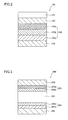
Fig. 2 is a sectional view of a thin-film photovoltaic element manufactured according to the present invention; and -
Fig. 3 is a sectional view showing a heterojunction photovoltaic element manufactured according to the present invention. - Embodiments of the present invention are now described with reference to the drawings.
- First, the structure of a catalytic wire CVD apparatus employed for manufacturing a semiconductor film according to a first embodiment of the present invention is described with reference to
Fig. 1 . - As shown in
Fig. 1 , the catalytic wire CVD apparatus comprises a reaction chamber 1, agas supply portion 2 for supplying source gas and pressure control gas into the reaction chamber 1, acatalytic wire 4 connected to aDC power source 3, anexhaust valve 5, aset portion 6 for setting anunderlayer 20 for forming asemiconductor film 10 and aheater 7 for heating theunderlayer 20 set on theset portion 6. - The
catalytic wire 4 is made of tungsten (W). Thiscatalytic wire 4 is heated by excitation with theDC power source 3. The reaction chamber 1 can be evacuated with a vacuum pump (not shown), and theexhaust valve 5 opens/closes an exhaust passage. - A method of manufacturing a semiconductor film according to the first embodiment of the present invention is described with reference to
Fig. 1 . According to the first embodiment, a hydrogenated amorphous silicon film is formed on theunderlayer 20 as thesemiconductor film 10. Table 1 shows exemplary conditions for manufacturing the amorphous silicon film.Table 1 Material for Catalytic Wire Tungsten Diameter of Catalytic Wire 0.5 mm Temperature of Catalytic Wire 1700 °C Temperature of Underlayer 200 ° C Pressure 3 Pa Flow Rate of SiH4 500 sccm Flow Rate of H2 1000 sccm - As shown in Table 1, the
catalytic wire 4 of tungsten having a diameter of about 0.5 mm is employed for forming the amorphous silicon film. Theunderlayer 20 is set on theset portion 6 of the catalytic wire CVD apparatus provided with thiscatalytic wire 4. Theunderlayer 20 is formed by an amorphous silicon film, a transparent conductive oxide film or a single-crystalline silicon substrate, for example. Formation of the amorphous silicon film is started in this state. Table 2 shows manufacturing process conditions for the amorphous silicon film according to the first embodiment.Table 2 Embodiment Step Introduction of Source Gas Pressure Control Heating of Catalytic Wire Film Formation Evacuation End Catalytic Wire ON ON ON OFF Source Gas ON ON ON ON OFF - In order to form the amorphous silicon film by the method of manufacturing a semiconductor film according to the first embodiment, the
underlayer 20 is heated to about 200°C with theheater 7 as shown in Table 1, and the source gas of SiH4 for forming the amorphous silicon film (semiconductor film 10) is introduced into the reaction chamber 1 from thegas supply portion 2, as shown in Table 2. The source gas of SiH4 is diluted with non-source gas of H2. As shown in Table 1, SiH4 and H2 are introduced at flow rates of about 500 sccm and about 1000 sccm respectively. Thereafter the pressure of the source gas is controlled according to the present invention. In other words, the pressure of the source gas is controlled to about 3 Pa (with partial pressures of about 1 Pa and about 2 Pa of SiH4 and H2 respectively), as shown in Table 1. Thereafter thecatalytic wire 4 is heated to about 1700°C by excitation with theDC power source 3, as shown in Table 2. - The
catalytic wire 4 heated to about 1700°C and the source gas of SiH4 present in the reaction chamber 1 come into contact with each other. Thus, thecatalytic wire 4 heated to about 1700°C decomposes SiH4, and the decomposed species is deposited on theunderlayer 20, for forming the hydrogenated amorphous silicon film (semiconductor film 10) on theunderlayer 20. - After the formation of the hydrogenated amorphous silicon film, the
exhaust valve 5 is opened for evacuating the reaction chamber 1 with the vacuum pump (not shown), as shown in Table 2. After the source gas (SiH4) is substantially exhausted from the reaction chamber 1, theDC power source 3 stops exciting thecatalytic wire 4. Thus, the temperature of thecatalytic wire 4 is reduced in the state where the source gas is substantially exhausted from the reaction chamber 1. The amorphous silicon film (semiconductor film 10) according to the first embodiment is formed in this manner. - According to the first embodiment, as hereinabove described, formation of the
semiconductor film 10 can be started in the state where the pressure of the atmosphere is stable by controlling the pressure of the atmosphere to about 3 Pa, thereafter heating thecatalytic wire 4 to about 1700°C and decomposing the source gas of SiH4 with the heatedcatalytic wire 4 thereby forming thesemiconductor film 10, whereby formation of thesemiconductor film 10 in a state where the pressure of the atmosphere is instable can be suppressed. Thus, the quality of thesemiconductor film 10 can be inhibited from destabilization. - The source gas of SiH4 is diluted with the non-source gas of H2, whereby the partial pressure of the source gas can be reduced to about 1 Pa when controlling the pressure of the atmosphere to about 3 Pa (total pressure of the source gas and the non-source gas). Thus, the pressure in the reaction chamber 1 can be controlled to about 3 Pa with a smaller quantity of the source gas as compared with a case of not diluting the source gas with the non-source gas. If heating of the
catalytic wire 4 is started in a state introducing the source gas of SiH4 into the reaction chamber 1, a constant time is required for heating thecatalytic wire 4 to about 1700°C, and hence thecatalytic wire 4 at a temperature of less than about 1700°C and the source gas of SiH4 come into contact with each other immediately after heating of thecatalytic wire 4 is started. At this time, the source gas of SiH4 easily remains on the insufficiently heated catalytic wire 4 (at the temperature of less than about 1700°C), and hence a compound (tungsten silicide) of thecatalytic wire 4 of tungsten (W) and the source gas of SiH4 may be formed on the surface of thecatalytic wire 4. According to the first embodiment, however, the pressure in the reaction chamber 1 is controlled to about 3 Pa with a relatively small quantity of the source gas of SiH4, whereby the surface of thecatalytic wire 4 can be prevented from formation of a silicide due to the small quantity of SiH4. Thus, the resistivity of thecatalytic wire 4 can be inhibited from variation resulting from formation of this compound, whereby difficulty in temperature control of thecatalytic wire 4 can be suppressed. - According to the first embodiment, as hereinabove described, the source gas is exhausted from the reaction chamber 1 after the formation of the
semiconductor film 10 and heating of thecatalytic wire 4 heated to about 1700°C is stopped after the source gas (SiH4) is substantially exhausted from the reaction chamber 1, whereby thecatalytic wire 4 and SiH4 can be prevented from coming into contact with each other in a state where the temperature of thecatalytic wire 4 is lower than about 1700°C. At the end of the manufacturing process for the amorphous silicon film (semiconductor film 10), therefore, formation of a compound (tungsten silicide) of thecatalytic wire 4 made of tungsten (W) and the source gas of SiH4 can be suppressed. Therefore, difficulty in temperature control of thecatalytic wire 4 can be suppressed similarly to the above. - According to a second embodiment of the present invention, a thin-film
photovoltaic element 100 is manufactured by the method of manufacturing a semiconductor film according to the aforementioned first embodiment. First, the structure of the thin-filmphotovoltaic element 100 manufactured by the method of manufacturing a semiconductor film according to the present invention is described with reference toFig. 2 . - As shown in
Fig. 2 , thephotovoltaic element 100 comprises asubstrate 101, asurface electrode layer 102, aphotoelectric conversion layer 103 and arear electrode layer 104. - The
substrate 101 has an insulating surface, and is made of glass having transparency. Thesurface electrode layer 102 is formed on the upper surface of thesubstrate 101. Thissurface electrode layer 102 is formed by a TCO (transparent conductive oxide) film of tin oxide (SnO2) or the like having conductivity and transparency. - The
photoelectric conversion layer 103 made of a p-in-type amorphous silicon-based semiconductor is formed on the upper surface of thesurface electrode layer 102. Thisphotoelectric conversion layer 103 of the p-i-n-type amorphous silicon-based semiconductor is constituted of a p-type hydrogenated amorphous silicon carbide (a-SiC:H)layer 103a (hereinafter referred to asa p layer 103a), an i-type hydrogenated amorphous silicon (a-Si:H)layer 103b (hereinafter referred to as ani layer 103b) and an n-type hydrogenated amorphous silicon (a-Si:H)layer 103c (hereinafter referred to as ann layer 103c). - The
rear electrode layer 104 is formed on the upper surface of thephotoelectric conversion layer 103. Therear electrode layer 104 is formed by holding the front and back surfaces of a silver (Ag) layer with a pair of ZnO layers. - A manufacturing process for the
photovoltaic element 100 shown inFig. 2 is now described. In the manufacturing process for thephotovoltaic element 100, thesurface electrode layer 102 of tin oxide is first formed on the upper surface of thesubstrate 101 having the insulating surface by thermal CVD (chemical vapor deposition). - Then, the p layer (p-type hydrogenated amorphous silicon carbide layer) 103a, the i layer (i-type hydrogenated amorphous silicon layer) 103b and the n layer (n-type hydrogenated amorphous silicon layer) 103c are successively formed on the upper surface of the
surface electrode layer 102 by catalytic wire CVD, thereby forming thephotoelectric conversion layer 103 of the amorphous silicon-based semiconductor. At this time, source gas diluted with hydrogen (H2) is introduced, the pressure of the atmosphere formed by the source gas is controlled and thereafter a catalytic wire 4 (seeFig. 1 ) is heated similarly to the aforementioned first embodiment, for forming the p layer (p-type hydrogenated amorphous silicon carbide layer) 103a on thesurface electrode layer 102 consisting of the transparent conductive oxide film, forming thei layer 103b on thep layer 103a and forming then layer 103c on thei layer 103b respectively. - Thereafter the
rear electrode layer 104 consisting of the metallic material layers (the ZnO layer (upper layer), the Ag layer (intermediate layer) and the ZnO layer (lower layer)) mainly composed of silver is formed on the upper surface of the photoelectric conversion layer 103 (n layer 103c) by sputtering. The thin-filmphotovoltaic element 100 is manufactured in this manner. - According to the second embodiment, as hereinabove described, the thin-film
photovoltaic element 100 is manufactured by forming thephotoelectric conversion layer 103 by the method of manufacturing a semiconductor film according to the aforementioned first embodiment, whereby the quality of thephotoelectric conversion layer 103 can be inhibited from destabilization. Thus, the thin-filmphotovoltaic element 100 can be manufactured with stable performance. - According to a third embodiment of the present invention, a heterojunction
photovoltaic element 200 is manufactured by the method of manufacturing a semiconductor film according to the aforementioned first embodiment. First, the structure of the heterojunctionphotovoltaic element 200 manufactured by the method of manufacturing a semiconductor film according to the present invention is described with reference toFig. 3 . - In the
photovoltaic element 200 according to the third embodiment, an amorphous silicon (a-Si)layer 202 functioning as a photoelectric conversion layer and asurface electrode layer 203 are successively formed on the upper surface of an n-type single-crystalline silicon (c-Si)substrate 201, as shown inFig. 3 . Thesurface electrode layer 203 is formed by a transparent conductive oxide film of ITO (indium tin oxide). Theamorphous silicon layer 202 is constituted of a substantially intrinsic i-typeamorphous silicon layer 202a formed on the upper surface of the n-type single-crystalline silicon substrate 201 and a p-typeamorphous silicon layer 202b doped with boron (B) formed on the i-typeamorphous silicon layer 202a. The i-typeamorphous silicon layer 202a has a small thickness, in order not to substantially contribute to power generation as an optical active layer. - An
amorphous silicon layer 204 functioning as a photoelectric conversion layer and arear electrode layer 205 are formed on the back surface of the n-type single-crystalline silicon substrate 201 successively from the side closer to the back surface of the n-type single-crystalline silicon substrate 201. Therear electrode layer 205 is formed by a transparent conductive oxide film of ITO. Theamorphous silicon layer 204 is constituted of a substantially intrinsic i-typeamorphous silicon layer 204a formed on the back surface of the n-type single-crystalline silicon substrate 201 and an n-type amorphous silicon layer 204b doped with phosphorus (P) formed on the back surface of the i-typeamorphous silicon layer 204a. The i-typeamorphous silicon layer 204a has a small thickness, in order not to substantially contribute to power generation. The i-typeamorphous silicon layer 204a, the n-type amorphous silicon layer 204b and therear electrode layer 205 constitute the so-called BSF (back surface field) structure. - A manufacturing process for the
photovoltaic element 200 is now described with reference toFig. 3 . - First, the n-type single-
crystalline silicon substrate 201 is cleaned and set in a vacuum chamber (not shown) and thereafter heated under a temperature condition of not more than 200°C, for removing moisture adhering to the surface of the n-type single-crystalline silicon substrate 201 to the utmost. Thus, oxygen contained in the moisture adhering to the surface of the n-type single-crystalline silicon substrate 201 is inhibited from binding to silicon and forming defects. - Then, hydrogen (H2) gas is introduced while keeping the substrate temperature at 170°C, for hydrogenating the upper surface of the n-type single-
crystalline silicon substrate 201. Thus, the upper surface of the n-type single-crystalline silicon substrate 201 is cleaned, and hydrogen atoms are adsorbed around the upper surface of the n-type single-crystalline silicon substrate 201. The adsorbed hydrogen atoms inactivate (terminate) defects on the upper surface of the n-type single-crystalline silicon substrate 201. - Thereafter the respective layers are formed on the front and back surfaces of the n-type single-
crystalline silicon substrate 201. - More specifically, the i-type
amorphous silicon layer 202a is formed on the upper surface of the n-type single-crystalline silicon substrate 201 by catalytic wire CVD. At this time, the i-typeamorphous silicon layer 202a is formed by introducing source gas diluted with hydrogen (H2), controlling the pressure of the atmosphere formed by the source gas and thereafter heating a catalytic wire 4 (seeFig. 1 ), similarly to the aforementioned first embodiment. - Then, the p-type
amorphous silicon layer 202b doped with boron (B) is formed on the i-typeamorphous silicon layer 202a by catalytic wire CVD. At this time, the p-typeamorphous silicon layer 202b is formed by introducing the source gas diluted with hydrogen (H2), controlling the pressure of the atmosphere formed by the source gas and thereafter heating the catalytic wire 4 (seeFig. 1 ), similarly to the aforementioned first embodiment. - Then, the
surface electrode layer 203 of ITO (indium tin oxide) is formed on the upper surface of the p-typeamorphous silicon layer 202b by sputtering. - Then, the i-type
amorphous silicon layer 204a is formed on the back surface of the n-type single-crystalline silicon substrate 201 by catalytic wire CVD. At this time, the i-typeamorphous silicon layer 204a is formed by introducing the source gas diluted with hydrogen (H2), controlling the pressure of the atmosphere formed by the source gas and thereafter heating the catalytic wire 4 (seeFig. 1 ), similarly to the aforementioned first embodiment. - Then, the n-type amorphous silicon layer 204b doped with phosphorus (P) is formed on the back surface of the i-type
amorphous silicon layer 204a by catalytic wire CVD. At this time, the n-type amorphous silicon layer 204b is formed by introducing source gas diluted with hydrogen (H2), controlling the pressure of the atmosphere formed by the source gas and thereafter heating the catalytic wire 4 (seeFig. 1 ), similarly to the aforementioned first embodiment. - Finally, the
rear electrode layer 205 of ITO is formed on the back surface of the n-type amorphous silicon layer 204b by sputtering. The heterojunctionphotovoltaic element 200 shown inFig. 3 is formed in this manner. - According to the third embodiment, as hereinabove described, the heterojunction
photovoltaic element 200 is manufactured by the method of manufacturing a semiconductor film according to the aforementioned first embodiment, whereby the qualities of the amorphous silicon layers 202 and 204 can be inhibited from destabilization when the heterojunctionphotovoltaic element 200 is manufactured by catalytic wire CVD. Thus, the heterojunctionphotovoltaic element 200 can be manufactured with stable performance, similarly to the aforementioned second embodiment. - Although the present invention has been described and illustrated in detail, it is clearly understood that the same is by way of illustration and example only and is not to be taken by way of limitation, the spirit and scope of the present invention being limited only by the terms of the appended claims.
- For example, while silane (SiH4) gas is employed as the source gas in the aforementioned first embodiment, the present invention is not restricted to this but another silane-based gas such as disilane (Si2H6) or trisilane (Si3H8) may alternatively be employed, or silicon fluoride-based gas such as SiF2 or SiH2F2 may be employed.
- While the
catalytic wire 4 is made of tungsten (W) in the aforementioned first embodiment, the present invention is not restricted to this but a catalytic wire made of another high-melting point material such as tantalum (Ta) may alternatively be employed. When the catalytic wire made of tantalum is employed, the surface of the catalytic wire can be more inhibited from formation of a silicide as compared with the case of employing thecatalytic wire 4 made of tungsten. - While the amorphous silicon film is formed on the
underlayer 20 as thesemiconductor film 10 under the film forming conditions shown in Table 1 in the aforementioned first embodiment, the present invention is not restricted to this but a semiconductor film of microcrystalline silicon or polycrystalline silicon may alternatively be formed on theunderlayer 20 as thesemiconductor film 10 by changing the film forming conditions. - While hydrogen (H2) gas is employed as the non-source gas diluting the source gas in the aforementioned first embodiment, the present invention is not restricted to this but rare gas such as argon (Ar) gas, fluorine (F2) gas, chlorine (Cl2) gas, nitrogen (N2) gas, carbon dioxide (CO2) gas or methane (CH4) gas may alternatively be employed as the non-source gas.
- While the pressure of the atmosphere is controlled to about 3 Pa in total with the partial pressures of about 1 Pa and about 2 Pa of the source gas and the non-source gas in the aforementioned first embodiment, the present invention is not restricted to this but the pressure of the atmosphere may not be controlled to about 3 Pa. The partial pressure of the source gas is preferably set to not more than about 1 Pa.
- While the reaction chamber 1 is evacuated with the vacuum pump in the aforementioned first embodiment, the present invention is not restricted to this but the reaction chamber 1 may alternatively be evacuated with supply of gas (H2 gas or Ar gas) containing no film forming species such as SiH4. Thus, the speed for exhausting SiH4 from the reaction chamber 1 can be increased. After film formation, the source gas (SiH4) may simply be exhausted, while the remaining gas (H2 gas or the like) may remain in the reaction chamber 1. When H2 gas remains in the reaction chamber 1, a compound (silicide) formed on the surface of the
catalytic wire 4 can be removed by etching. - While the thin-film
photovoltaic element 100 and the heterojunctionphotovoltaic element 200 are manufactured in the aforementioned second and third embodiments respectively, the present invention is not restricted to these but is generally applicable to a photoelectric element having a semiconductor film manufactured by catalytic wire CVD. Further, the present invention is not restricted to the photovoltaic element but is generally applicable to a semiconductor element having a semiconductor film manufactured by catalytic wire CVD.
Claims (18)
- A method of manufacturing a semiconductor film comprising steps of:introducing source gas for a semiconductor; controlling the pressure of an atmosphere formed by said source gas to a prescribed level;heating a catalytic wire (4) to at least a prescribed temperature after controlling the pressure of said atmosphere to said prescribed level; andforming a semiconductor film (10) by decomposing said source gas with heated said catalytic wire.
- The method of manufacturing a semiconductor film according to claim 1, wherein
said source gas is diluted with non-source gas. - The method of manufacturing a semiconductor film according to claim 2, wherein
said source gas includes silane-based gas, and
said non-source gas includes hydrogen gas. - The method of manufacturing a semiconductor film according to claim 1, further comprising steps of:exhausting said source gas after forming said semiconductor film, andstopping heating said catalytic wire heated to at least said prescribed temperature after substantially exhausting said source gas.
- The method of manufacturing a semiconductor film according to claim 1, wherein
said semiconductor film includes an amorphous silicon film. - The method of manufacturing a semiconductor film according to claim 1, wherein
said source gas includes silane gas, and
said prescribed temperature is at least 1700°C. - The method of manufacturing a semiconductor film according to claim 1, wherein
said catalytic wire is made of tungsten. - The method of manufacturing a semiconductor film according to claim 1, wherein
said step of forming said semiconductor film includes a step of depositing said decomposed source gas on an underlayer (20) thereby forming said semiconductor film on said underlayer. - The method of manufacturing a semiconductor film according to claim 8, wherein
said underlayer includes an amorphous silicon film (103a, 103b), a transparent conductive oxide film (102) or a single-crystalline silicon substrate (201). - A method of manufacturing a photovoltaic element comprising steps of:introducing source gas for a semiconductor; controlling the pressure of an atmosphere formed by said source gas to a prescribed level;heating a catalytic wire (4) to at least a prescribed temperature after controlling the pressure of said atmosphere to said prescribed level; and forming a semiconductor film (10) functioning as a photoelectric conversion layer by decomposing said source gas with heated said catalytic wire.
- The method of manufacturing a photovoltaic element according to claim 10, wherein
said source gas is diluted with non-source gas. - The method of manufacturing a photovoltaic element according to claim 11, wherein
said source gas includes silane-based gas, and
said non-source gas includes hydrogen gas. - The method of manufacturing a photovoltaic element according to claim 10, further comprising steps of:exhausting said source gas after forming said semiconductor film, andstopping heating said catalytic wire heated to at least said prescribed temperature after substantially exhausting said source gas.
- The method of manufacturing a photovoltaic element according to claim 10, wherein
said semiconductor film includes an amorphous silicon film. - The method of manufacturing a photovoltaic element according to claim 10, wherein
said source gas includes silane gas, and
said prescribed temperature is at least 1700°C. - The method of manufacturing a photovoltaic element according to claim 10, wherein
said catalytic wire is made of tungsten. - The method of manufacturing a photovoltaic element according to claim 10, wherein
said step of forming said semiconductor film includes a step of depositing said decomposed source gas on an underlayer (20) thereby forming said semiconductor film on said underlayer. - The method of manufacturing a photovoltaic element according to claim 17, wherein
said underlayer includes an amorphous silicon film (103a, 103b), a transparent conductive oxide film (102) or a single-crystalline silicon substrate (201).
Applications Claiming Priority (1)
| Application Number | Priority Date | Filing Date | Title |
|---|---|---|---|
| JP2007112333A JP2008270572A (en) | 2007-04-20 | 2007-04-20 | Photovoltaic element manufacturing method |
Publications (2)
| Publication Number | Publication Date |
|---|---|
| EP1983579A2 true EP1983579A2 (en) | 2008-10-22 |
| EP1983579A3 EP1983579A3 (en) | 2010-07-21 |
Family
ID=39677428
Family Applications (1)
| Application Number | Title | Priority Date | Filing Date |
|---|---|---|---|
| EP08251466A Ceased EP1983579A3 (en) | 2007-04-20 | 2008-04-18 | Method of manufacturing semiconductor film and method of manufacturing photovoltaic element |
Country Status (5)
| Country | Link |
|---|---|
| US (1) | US8043885B2 (en) |
| EP (1) | EP1983579A3 (en) |
| JP (1) | JP2008270572A (en) |
| KR (1) | KR20080094633A (en) |
| CN (1) | CN101290878A (en) |
Families Citing this family (3)
| Publication number | Priority date | Publication date | Assignee | Title |
|---|---|---|---|---|
| US20110086462A1 (en) * | 2009-10-08 | 2011-04-14 | Ovshinsky Stanford R | Process for Manufacturing Solar Cells including Ambient Pressure Plasma Torch Step |
| JP5891366B2 (en) * | 2011-03-24 | 2016-03-23 | パナソニックIpマネジメント株式会社 | Method for producing transparent conductive film and method for producing solar cell |
| DE102011018324A1 (en) * | 2011-04-20 | 2012-10-25 | Forschungszentrum Jülich GmbH | Hot wire method for depositing semiconductor material on a substrate and apparatus for carrying out the method |
Citations (5)
| Publication number | Priority date | Publication date | Assignee | Title |
|---|---|---|---|---|
| US6124186A (en) * | 1992-05-05 | 2000-09-26 | Midwest Research Institute | Deposition of device quality, low hydrogen content, hydrogenated amorphous silicon at high deposition rates with increased stability using the hot wire filament technique |
| JP2002069646A (en) * | 2000-09-01 | 2002-03-08 | Sony Corp | Thin film manufacturing method |
| JP3453214B2 (en) | 1995-03-15 | 2003-10-06 | 科学技術振興事業団 | Method of manufacturing thin film transistor by catalytic CVD method and thin film transistor |
| JP2005317670A (en) * | 2004-04-27 | 2005-11-10 | Japan Science & Technology Agency | (100) Method for producing oriented cubic silicon carbide crystal film |
| JP2007046135A (en) * | 2005-08-12 | 2007-02-22 | Seiko Instruments Inc | Thin film manufacturing method |
Family Cites Families (16)
| Publication number | Priority date | Publication date | Assignee | Title |
|---|---|---|---|---|
| US4409424A (en) * | 1982-06-21 | 1983-10-11 | Genevieve Devaud | Compensated amorphous silicon solar cell |
| EP0949688A1 (en) * | 1998-03-31 | 1999-10-13 | Phototronics Solartechnik GmbH | Thin film solar cell, method of manufacturing the same, and apparatus for carrying out the method of manufacturing |
| JP2000223419A (en) | 1998-06-30 | 2000-08-11 | Sony Corp | Method for forming single crystal silicon layer, method for manufacturing semiconductor device, and semiconductor device |
| JP2001168038A (en) * | 1999-12-10 | 2001-06-22 | Sony Corp | Single crystal silicon layer, its epitaxial growth method, and semiconductor device |
| JP4710187B2 (en) * | 2000-08-30 | 2011-06-29 | ソニー株式会社 | Method for growing polycrystalline silicon layer and method for epitaxial growth of single crystal silicon layer |
| US7122736B2 (en) * | 2001-08-16 | 2006-10-17 | Midwest Research Institute | Method and apparatus for fabricating a thin-film solar cell utilizing a hot wire chemical vapor deposition technique |
| JP2003193235A (en) | 2001-12-28 | 2003-07-09 | Nippon Steel Corp | Structure having curved surface shape, manufacturing apparatus and manufacturing method thereof |
| JP3748060B2 (en) | 2002-01-16 | 2006-02-22 | 京セラ株式会社 | Cleaning method for plasma CVD apparatus |
| JP2004064042A (en) | 2002-06-03 | 2004-02-26 | Hitachi Ltd | Solar cell device, method of manufacturing the same, metal plate for the solar cell device, and power generation plant |
| EP1369931A1 (en) | 2002-06-03 | 2003-12-10 | Hitachi, Ltd. | Solar cell and its manufacturing method, metal plate for the same |
| JP4405161B2 (en) | 2003-02-04 | 2010-01-27 | シャープ株式会社 | Polycrystalline silicon substrate processing method, polycrystalline silicon substrate processed by the method, and solar cell |
| JP2005179744A (en) * | 2003-12-19 | 2005-07-07 | Toshiba Corp | Catalytic CVD apparatus and catalytic CVD method |
| JP2005179743A (en) * | 2003-12-19 | 2005-07-07 | Toshiba Corp | Catalytic CVD apparatus and catalytic CVD method |
| JP2006024735A (en) * | 2004-07-08 | 2006-01-26 | Seiko Instruments Inc | Semiconductor film crystallization method and display device manufacturing method |
| JP2006176811A (en) | 2004-12-21 | 2006-07-06 | Rikogaku Shinkokai | Method for producing crystalline SiC film |
| JP4308281B2 (en) * | 2007-04-23 | 2009-08-05 | 三洋電機株式会社 | Photovoltaic element manufacturing method |
-
2007
- 2007-04-20 JP JP2007112333A patent/JP2008270572A/en active Pending
-
2008
- 2008-04-18 EP EP08251466A patent/EP1983579A3/en not_active Ceased
- 2008-04-18 CN CNA2008100925327A patent/CN101290878A/en active Pending
- 2008-04-18 US US12/105,469 patent/US8043885B2/en not_active Expired - Fee Related
- 2008-04-21 KR KR1020080036704A patent/KR20080094633A/en not_active Ceased
Patent Citations (5)
| Publication number | Priority date | Publication date | Assignee | Title |
|---|---|---|---|---|
| US6124186A (en) * | 1992-05-05 | 2000-09-26 | Midwest Research Institute | Deposition of device quality, low hydrogen content, hydrogenated amorphous silicon at high deposition rates with increased stability using the hot wire filament technique |
| JP3453214B2 (en) | 1995-03-15 | 2003-10-06 | 科学技術振興事業団 | Method of manufacturing thin film transistor by catalytic CVD method and thin film transistor |
| JP2002069646A (en) * | 2000-09-01 | 2002-03-08 | Sony Corp | Thin film manufacturing method |
| JP2005317670A (en) * | 2004-04-27 | 2005-11-10 | Japan Science & Technology Agency | (100) Method for producing oriented cubic silicon carbide crystal film |
| JP2007046135A (en) * | 2005-08-12 | 2007-02-22 | Seiko Instruments Inc | Thin film manufacturing method |
Also Published As
| Publication number | Publication date |
|---|---|
| US8043885B2 (en) | 2011-10-25 |
| JP2008270572A (en) | 2008-11-06 |
| EP1983579A3 (en) | 2010-07-21 |
| CN101290878A (en) | 2008-10-22 |
| US20080261347A1 (en) | 2008-10-23 |
| KR20080094633A (en) | 2008-10-23 |
Similar Documents
| Publication | Publication Date | Title |
|---|---|---|
| EP2624307B1 (en) | Method for manufacturing photoelectric conversion device | |
| CN101283455B (en) | Silicon-based thin-film photoelectric conversion device, and method and apparatus for manufacturing same | |
| US20050115504A1 (en) | Method and apparatus for forming thin films, method for manufacturing solar cell, and solar cell | |
| KR20090035471A (en) | Multi-junction Solar Cells and Methods and Apparatuses for Forming The Same | |
| US7638413B2 (en) | Method of fabricating semiconductor by nitrogen doping of silicon film | |
| EP1548848A1 (en) | Amorphous silicon solar cell | |
| JP6612359B2 (en) | Method for manufacturing photoelectric conversion device | |
| EP1986242B1 (en) | Method of manufacturing a photovoltaic element using hot wire CVD | |
| JP6609324B2 (en) | Method for manufacturing photoelectric conversion device | |
| US6531654B2 (en) | Semiconductor thin-film formation process, and amorphous silicon solar-cell device | |
| JP4709662B2 (en) | Method for forming transparent electrode film and method for manufacturing solar cell | |
| US8043885B2 (en) | Method of manufacturing semiconductor film and method of manufacturing photovoltaic element | |
| EP2330633A1 (en) | Photoelectric conversion device manufacturing method, photoelectric conversion device, and photoelectric conversion device manufacturing system | |
| US11069828B2 (en) | Method for manufacturing photoelectric conversion device | |
| JP4711851B2 (en) | Photovoltaic device | |
| JP3697199B2 (en) | Solar cell manufacturing method and solar cell | |
| JP3746711B2 (en) | Method for manufacturing microcrystalline silicon solar cell | |
| EP2336388B1 (en) | Method for deposition of a layer of a tin oxide onto a substrate | |
| JP2006083436A (en) | Method for producing transparent conductive film | |
| JP2011117082A (en) | Method for depositing transparent electrode film and method for producing solar battery | |
| KR20110068313A (en) | Texturing module and solar cell manufacturing apparatus having same and solar cell manufacturing method using same |
Legal Events
| Date | Code | Title | Description |
|---|---|---|---|
| PUAI | Public reference made under article 153(3) epc to a published international application that has entered the european phase |
Free format text: ORIGINAL CODE: 0009012 |
|
| AK | Designated contracting states |
Kind code of ref document: A2 Designated state(s): AT BE BG CH CY CZ DE DK EE ES FI FR GB GR HR HU IE IS IT LI LT LU LV MC MT NL NO PL PT RO SE SI SK TR |
|
| AX | Request for extension of the european patent |
Extension state: AL BA MK RS |
|
| PUAL | Search report despatched |
Free format text: ORIGINAL CODE: 0009013 |
|
| AK | Designated contracting states |
Kind code of ref document: A3 Designated state(s): AT BE BG CH CY CZ DE DK EE ES FI FR GB GR HR HU IE IS IT LI LT LU LV MC MT NL NO PL PT RO SE SI SK TR |
|
| AX | Request for extension of the european patent |
Extension state: AL BA MK RS |
|
| RIC1 | Information provided on ipc code assigned before grant |
Ipc: H01L 31/20 20060101ALI20100617BHEP Ipc: H01L 31/18 20060101ALI20100617BHEP Ipc: C23C 16/44 20060101ALI20100617BHEP Ipc: H01L 21/205 20060101ALI20100617BHEP Ipc: C23C 16/24 20060101AFI20100617BHEP |
|
| RAP1 | Party data changed (applicant data changed or rights of an application transferred) |
Owner name: SANYO ELECTRIC CO., LTD. |
|
| 17P | Request for examination filed |
Effective date: 20101216 |
|
| AKX | Designation fees paid |
Designated state(s): AT BE BG CH CY CZ DE DK EE ES FI FR GB GR HR HU IE IS IT LI LT LU LV MC MT NL NO PL PT RO SE SI SK TR |
|
| 17Q | First examination report despatched |
Effective date: 20130102 |
|
| RAP1 | Party data changed (applicant data changed or rights of an application transferred) |
Owner name: PANASONIC INTELLECTUAL PROPERTY MANAGEMENT CO., LT |
|
| 17Q | First examination report despatched |
Effective date: 20170317 |
|
| STAA | Information on the status of an ep patent application or granted ep patent |
Free format text: STATUS: THE APPLICATION HAS BEEN REFUSED |
|
| 18R | Application refused |
Effective date: 20181217 |