EP1982198B1 - Test system for a circuit carrier - Google Patents
Test system for a circuit carrier Download PDFInfo
- Publication number
- EP1982198B1 EP1982198B1 EP07702635A EP07702635A EP1982198B1 EP 1982198 B1 EP1982198 B1 EP 1982198B1 EP 07702635 A EP07702635 A EP 07702635A EP 07702635 A EP07702635 A EP 07702635A EP 1982198 B1 EP1982198 B1 EP 1982198B1
- Authority
- EP
- European Patent Office
- Prior art keywords
- signal
- test
- testing system
- circuit carrier
- frequency structure
- Prior art date
- Legal status (The legal status is an assumption and is not a legal conclusion. Google has not performed a legal analysis and makes no representation as to the accuracy of the status listed.)
- Active
Links
Images


Classifications
-
- G—PHYSICS
- G01—MEASURING; TESTING
- G01R—MEASURING ELECTRIC VARIABLES; MEASURING MAGNETIC VARIABLES
- G01R1/00—Details of instruments or arrangements of the types included in groups G01R5/00 - G01R13/00 and G01R31/00
- G01R1/02—General constructional details
- G01R1/06—Measuring leads; Measuring probes
- G01R1/067—Measuring probes
- G01R1/06772—High frequency probes
-
- G—PHYSICS
- G01—MEASURING; TESTING
- G01R—MEASURING ELECTRIC VARIABLES; MEASURING MAGNETIC VARIABLES
- G01R31/00—Arrangements for testing electric properties; Arrangements for locating electric faults; Arrangements for electrical testing characterised by what is being tested not provided for elsewhere
- G01R31/28—Testing of electronic circuits, e.g. by signal tracer
- G01R31/2801—Testing of printed circuits, backplanes, motherboards, hybrid circuits or carriers for multichip packages [MCP]
- G01R31/2806—Apparatus therefor, e.g. test stations, drivers, analysers, conveyors
-
- G—PHYSICS
- G01—MEASURING; TESTING
- G01R—MEASURING ELECTRIC VARIABLES; MEASURING MAGNETIC VARIABLES
- G01R1/00—Details of instruments or arrangements of the types included in groups G01R5/00 - G01R13/00 and G01R31/00
- G01R1/20—Modifications of basic electric elements for use in electric measuring instruments; Structural combinations of such elements with such instruments
- G01R1/24—Transmission-line, e.g. waveguide, measuring sections, e.g. slotted section
-
- G—PHYSICS
- G01—MEASURING; TESTING
- G01R—MEASURING ELECTRIC VARIABLES; MEASURING MAGNETIC VARIABLES
- G01R27/00—Arrangements for measuring resistance, reactance, impedance, or electric characteristics derived therefrom
- G01R27/28—Measuring attenuation, gain, phase shift or derived characteristics of electric four pole networks, i.e. two-port networks; Measuring transient response
Definitions
- the invention relates to a test system for analyzing a circuit carrier equipped with a high-frequency structure.
- circuit carrier for high-frequency applications, which is provided for the assembly of wired components and / or SMD components, it is common for cost reasons, perform a circuit carrier test to the circuit board before the assembly of the components for material and function-specific errors examine and, in the event that the circuit board is faulty, take it out of the production chain.
- test system With a standard test system, connections on the circuit board are checked for short circuits and open circuits by a continuity measurement.
- a test system with the designation "Polar” is known by the company Polar Instruments, which can be used for testing circuit carriers and can be used for short-circuit troubleshooting and for impedance analysis on the circuit board to be tested.
- the testing system of the company Polar Instruments operates by means of voltage-time reflectometry in the lower high-frequency range up to a maximum frequency of about 300 MHz. Due to the comparatively low maximum frequency, the test system is unsuitable for testing circuit carriers for high-frequency applications which can be operated in the frequency range up to 40 GHz.
- the measuring method of voltage-time reflectometry with the "Polar" test system can not be used for determining transmission and reflection parameters of a high frequency structure arranged on the circuit carrier, from which numerous material and function-specific parameters of the test object could be derived.
- the invention is based on the object of specifying a test system, with which material-specific and function-specific high-frequency characteristics and the functionality of a circuit carrier equipped with a high-frequency structure can be analyzed over a particularly large frequency range.
- the test system for analyzing a circuit carrier equipped with a high-frequency structure comprises a network analyzer and a contact device.
- the network analyzer has a signal generator for generating an excitation signal, which can be supplied to the circuit carrier via a signal line of the high-frequency structure.
- the network analyzer comprises an evaluation device, to which a measuring signal returning from the high-frequency structure can be fed for analysis and comparison with the excitation signal. The excitation signal and the returning measurement signal can be fed into the high-frequency structure via the signal line and the contact device which can be connected to it.
- the contact device is preferably equipped with a measuring tip, to which test probes are fastened, with which a direct contact between the high-frequency structure and the contact device can be produced.
- the test probes contact the circuit carrier, arranged for supplying the excitation signal and for feeding the measurement signal provided test points, which are signal-connectable to the high-frequency structure of the circuit substrate.
- the high-frequency structure is in particular a formed on the circuit carrier stripline, so for example, a high-frequency filter to understand.
- the circuit carrier equipped with the high-frequency structure can be analyzed over a comparatively large frequency range up to several gigahertz.
- the network analyzer which can be connected to the high-frequency structure of the circuit carrier via a contact device, a complete system analysis of the high-frequency structure can be carried out in addition to the determination of transmission and reflection parameters.
- the analysis of the high-frequency structure of the circuit carrier also allows a determination of the circuit substrate material and its dielectric properties as well as an investigation of the signal propagation times occurring in the high-frequency structure over the predetermined frequency range.
- test system according to the invention a particularly greatly reduced number of faulty and fully assembled, i. accessible with wired and SMD components, circuit carriers reachable.
- circuit board manufacturing costs of each individual fertigmont mandat and error-free circuit substrate can be reduced by a multiple, since the production process is stopped in faulty circuit carriers before the costly assembly with wired and SMD components.
- the circuit carrier equipped with the high-frequency structure it is expedient to provide a connection between the high-frequency structure and a surrounding circuit structure arranged on the circuit carrier or provide several bridgeable blank strips.
- the or the empty strips is or are optionally part of the circuit substrate material.
- the high frequency structure is electrically isolated from the surrounding circuit structure for analysis.
- the analysis of the high frequency structure is thus carried out trouble-free.
- the blank strip or strips can be bridged by means of a bridge in order to produce an electrically conductive connection between the high-frequency structure and the surrounding circuit structure of the circuit board and to be able to use the circuit board in an application-specific manner.
- the high-frequency structure provided for analyzing the circuit carrier is arranged on a useful edge connected to the circuit carrier, which optionally can be removed after carrying out the analysis and / or completion of the circuit carrier.
- the high-frequency structure arranged at the useful edge also serves, in particular, to analyze the high-frequency properties of the circuit carrier material and, in the case of a multilayer circuit carrier, the influence of the individual carrier layers on the high-frequency structure.
- the circuit carrier is mounted in a holding and positioning device in order to fix the circuit carrier and to bring the test point of the circuit carrier closer to the test probes of the measuring tip.
- the contact device can be fixed to the holding and positioning device in order to move the test probes arranged on the measuring tip for contacting the test point thereto.
- the test probes arranged on the measuring tip are designed such that for contacting one at the test site provided mass plate at least one Masseprüfnadel and for contacting a provided at the test point signal plate a Signalprüfnadel, whereby the excitation signal is fed into the high-frequency structure, are provided.
- a distance of about 500-1500 microns is provided between a contact surface of the signal plate, which is the coupling point of the Signalprüfnadel and the signal plate, and a contact surface of the ground plate.
- test needles In order to electrically isolate the test probes arranged on one and the same measuring tip from one another, it is further expedient to provide the test needles individually with a protective casing.
- the protective coating on the respective test needle is designed such that the test needle is sheath-free at the coupling point for contacting the test site.
- calibration structures are provided for the test system, whereby parasitic interference can be eliminated, which can arise at plug or adapter transitions and at the coupling points of the test probes.
- the circuit carrier is made of a material having dielectric properties, which is particularly suitable for use in the high-frequency range.
- the materials include in particular polytetrafluoroethylene, polyimides and glass and ceramic alloys.
- a multilayer design of the circuit carrier is expedient in that a comparatively large number of high-frequency structures, for example high-frequency filters, can be realized as strip lines on the circuit carrier.
- the multilayer design is a space-saving variant, why a provided on the circuit substrate for connection of the electronic components line structure is particularly easy to implement.
- the circuit carrier for mounting with wired components is designed such that for fixing the wired components on the circuit substrate and the electrical connection of the wired components are provided with provided on the circuit board connection lines on the circuit board through holes formed between opposite side surfaces of the circuit substrate are. Furthermore, the circuit carrier for mounting with surface-mountable SMD components is designed such that on the surfaces of the circuit substrate contact surfaces on the one hand for fixing and on the other hand for electrically contacting the SMD components are provided with provided on the circuit board connection lines.
- the signal generator provided on the network analyzer for generating the excitation signal can be controlled in such a way to traverse the excitation signal over a frequency range which can be predetermined (frequency sweep).
- the frequency sweep is used for a particularly comprehensive analysis of the circuit carrier over the predefinable frequency range with particularly exact frequency resolution.
- the excitation signal can be coupled out at the network analyzer and, for the analysis of the circuit carrier, can be compared as a reference signal with the returning measuring signal.
- Fig. 1 shows a schematic diagram of the test system 1 with a network analyzer 2 and with a first contact device 4 and a second contact device 6.
- the network analyzer 2 comprises a signal generator 8 for generating the excitation signal 10, which is fed via a signal line 12 a switching device 14.
- the network analyzer 2 further comprises a first measuring bridge 16 and a second measuring bridge 18, which are signal-connected to the switching device 14 via signal lines 20, 22.
- the contact devices 4, 6 are signal-connected via signal lines 24, 26 to the network analyzer 2.
- the excitation signal 10 can be fed to the contact devices 4, 6 via the signal lines 24, 26.
- the contact means 4,6 each comprise a measuring tip 32,34 and each as a signal probes 36,38 and as ground probes 40,42 formed contact pins.
- the signal probes 36, 38 contact signal plates 48, 50 arranged at test points 44, 46 provided on the circuit carrier 28.
- the mass probes 40,42 contact at the test sites 44,46 provided mass plates 52,54.
- the switching device 14 is caused to supply the excitation signal 10 to the first contact device 4 via the signal line 20 and the signal line 24 or the second contact device 6 via the signal line 22 and the signal line 26.
- the high-frequency structure 30 can also be viewed as a measurement object, the excitation signal 10 being supplied to the object to be analyzed either via the test point 44 serving as the input gate or via the test point 46 serving as the output port.
- s-parameters are determined.
- the excitation signal 10 at the test site 44 of FIG High frequency structure 30 supplied.
- a measuring signal 56 transmitted through the high-frequency structure 30 and returning to the signal line 26 is coupled to the second measuring bridge 18 for evaluation on a signal line 60 leading to an evaluation device 58.
- the "forward transmission factor s 21 " is thus from the returning measurement signal 56 and the excitation signal 10, which is coupled as a reference signal 62 to a leading to the evaluation device 58 signal line 64, determined.
- the excitation signal 10 is supplied to the high-frequency structure 30 via the second contact device 6.
- a measuring signal 66 transmitted to the first contact device 4 and transmitted back to the signal line 24 through the high-frequency structure 30 is coupled out at the first measuring bridge 16 to a signal line 67 leading to the evaluation device 58.
- the measurement signal 66 supplied to the evaluation device 58 is subsequently compared with the reference signal 62 coupled to the second measuring bridge 18 and supplied via a signal line 68 to the evaluation device 58 for determining the "reverse transmission factor s 12 ".
- properties of the high-frequency structures on the circuit carrier can be derived over a desired frequency range such as, for example, transmission and reflection attenuation, signal propagation times, signal rise times, impedance curves, step responses and phase information.
- parameters of the circuit substrate such as its material, the dielectric properties of the material and - in multi-layer circuit boards - the quality of their layer structure can be determined.
- the high-frequency structure 30 can be electrically isolated from the surrounding circuit structure 69 by means of one or more bridgeable empty strips 70.
- Fig. 2 shows a schematic structure of the test system 1, wherein the circuit substrate 28 is mounted in a holding and positioning device 71.
- the holding and positioning device 71 is mounted on a base plate 72, whereupon a lower fixed fixed plate 74 and an upper movable plate 76 are arranged.
- the circuit carrier 28 is positioned directly on the movable plate 76, which can be raised and lowered in the lifting direction 78 and is pivotable in displacement directions 80, 82.
- the contact devices 4, 6 are connected to the network analyzer 2 via the signal lines 24, 26, which are designed, for example, as coaxial cables.
- Fig. 3 shows a section 94 of the circuit substrate 28 with the contact devices 4,6 with connectors 96,98 formed, for example, as coaxial cable signal lines 24,26, about which the excitation signal 10 based on the test needles 36,38,40A, 40B, 42A, 42B at the test stations 44th , 46 can be fed in and the returning measuring signal 56, 66 can be fed out.
- the contact devices 4, 6 are connected via their rear parts 100, 102 to the in Fig. 2 shown retaining blocks 92 held.
- the test probes 36, 38, 40 A, 40 B, 42 A, 42 B carrying measuring tips 32, 34 are arranged on front parts 104, 106 of the contact devices 4, 6.
- each measuring tip 32, 34 carries a signal testing needle 36, 38 and in each case two mass testing needles 40 A, 40 B, 42 A, 42 B which are at a distance from and electrically insulated from the signal testing needle 36, 38.
- the test probes 36, 38, 40 A, 40 B, 42 A, 42 B contact the end points provided on the circuit board 28 Kirstellen 44.46.
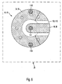
- the test centers are 44.46 in Fig. 3 embodiment shown formed horseshoe-shaped on the circuit substrate 28.
- the signal plate 48,50 is formed, which with the in Fig. 3 for simplicity, not shown high frequency structure 30 ( Fig. 2 ) is signal connectable.
- the signal pad 48, 50 is electrically isolated from the ground pad 52, 54 by a dummy dielectric strip 108, 110. Furthermore, also the mass plate 52, 54 with respect to a Fig. 3 not shown, the test site 44,46 surrounding circuit structure arranged electrically insulated by dummy strips 112,114.
- Fig. 4 the probe tip 32, 34 is shown in detail, which is arranged on the front part 104, 106 of the contact device 4, 6, and a signal test probe 36, 38, and two probe probes 36, 38 and electrically isolated from them, mass probes 40A, 40B, 42A, 42B wearing.
- Signalprüfnadel 36,38 between the two mass probes 40A, 40B, 42A, 42B arranged.
- FIGS. 5A, 5B, 5C is the measuring tip 32,34 with arranged on this test needles 36,38,40,42,40A, 40B, 42A, 42B shown in different arrangement variants and with a different number of probes.
- Fig. 5A are the test needles 36,38,40A, 40B, 42A, 42B at the measuring tip 32,34 in the same manner as in Fig. 4 arranged.
- the test probes 36, 38, 40A, 40B, 42A, 42B are according to the scheme mass-signal ground at a designated terminal end 115 of the probe tip 32,34 fixed to this.
- Fig. 6 shows the test site 44.46 according to Fig. 3 in detail.
- the test site 44,46 is disposed on a surface of the circuit substrate 28 and has the in accordance with the embodiment Fig. 6 horseshoe-shaped mass plates 54,56 and the signal plate 48,50, which with the in Fig. 6 not shown high frequency structure 30 is signal connectable.
- the signal plate 48.50 is electrically insulated from the ground plate 54, 56 by the horseshoe-shaped, dielectric empty strip 108, 110, which in the exemplary embodiment according to FIG Fig. 6 Part of the circuit carrier 28 indicated by a dashed line.
- the invention is not limited to the illustrated embodiments and is particularly designed differently than in the drawing Circuit carriers and test systems, in particular in a test system with a single contact device or more than two contact devices for n-gate measurement objects suitable.
- the present invention is also particularly suitable for differential measurements with differential test signals.
- a signal with 180 ° phase shift (differential mode) is generated at two gates of the network analyzer and fed into the high-frequency structure.
- the measurement signal is also differentially fed out, i.
- On the output side there are again two test ports of the network analyzer available and, in particular, compliance with the phase difference of 180 ° is checked by the high-frequency structure to be measured.
- the differential measurement has the advantage that it is insensitive to ambient common mode noise, which can be caused for example by the electrical supply network but also by other sources of interference.
- today high-frequency structures are increasingly being built with differential wiring.
Description
Die Erfindung bezieht sich auf ein Prüfsystem zur Analyse eines mit einer Hochfrequenzstruktur bestückten Schaltungsträgers.The invention relates to a test system for analyzing a circuit carrier equipped with a high-frequency structure.
Bei einem Schaltungsträger für Hochfrequenzanwendungen, welcher für die Bestückung mit bedrahteten Bauelementen und/oder SMD-Bauelementen vorgesehen ist, ist es vorwiegend aus Kostengründen üblich, eine Schaltungsträgerprüfung durchzuführen, um den Schaltungsträger bereits vor der Bestückung mit den Bauelementen nach material- und funktionsspezifischen Fehlern zu untersuchen und für den Fall, dass der Schaltungsträger fehlerbehaftet ist, diesen aus der Produktionskette herauszunehmen.In a circuit carrier for high-frequency applications, which is provided for the assembly of wired components and / or SMD components, it is common for cost reasons, perform a circuit carrier test to the circuit board before the assembly of the components for material and function-specific errors examine and, in the event that the circuit board is faulty, take it out of the production chain.
Mit einem gewöhnlichen Prüfsystem werden Verbindungen auf dem Schaltungsträger anhand einer Durchgangsmessung auf Kurzschlüsse sowie auf Leerläufe überprüft. Ein derartiges Prüfsystem mit der Bezeichnung "Polar" ist von der Firma Polar Instruments bekannt, welches zum Testen von Schaltungsträgern verwendbar und zur Kurzschluss-Fehlersuche sowie zur Impedanzanalyse am zu testenden Schaltungsträger einsetzbar ist. Im Wege der Impedanzanalyse arbeitet das Prüfsystem der Firma Polar Instruments mittels Spannungs-Zeitreflektometrie im unteren Hochfrequenzbereich bis zu einer maximalen Frequenz von etwa 300 MHz. Das Prüfsystem ist schon aufgrund der vergleichsweise niedrigen Maximalfrequenz zum Test von Schaltungsträgern für Hochfrequenzanwendungen, welche im Frequenzbereich bis zu 40 GHz betreibbar sind, ungeeignet. Des weiteren ist das Messverfahren der Spannungs-Zeitreflektometrie mit dem Prüfsystem "Polar" nicht zur Ermittlung von Transmissions- und Reflexionsparametern einer auf dem Schaltungsträger angeordneten Hochfrequenzstruktur einsetzbar, woraus zahlreiche material- und funktionsspezifische Parameter des Messobjekts ableitbar wären.With a standard test system, connections on the circuit board are checked for short circuits and open circuits by a continuity measurement. Such a test system with the designation "Polar" is known by the company Polar Instruments, which can be used for testing circuit carriers and can be used for short-circuit troubleshooting and for impedance analysis on the circuit board to be tested. By means of impedance analysis, the testing system of the company Polar Instruments operates by means of voltage-time reflectometry in the lower high-frequency range up to a maximum frequency of about 300 MHz. Due to the comparatively low maximum frequency, the test system is unsuitable for testing circuit carriers for high-frequency applications which can be operated in the frequency range up to 40 GHz. Furthermore, the measuring method of voltage-time reflectometry with the "Polar" test system can not be used for determining transmission and reflection parameters of a high frequency structure arranged on the circuit carrier, from which numerous material and function-specific parameters of the test object could be derived.
Der Erfindung liegt die Aufgabe zu Grunde, ein Prüfsystem anzugeben, womit materialspezifische und funktionsspezifische Hochfrequenzeigenschaften sowie die Funktionstüchtigkeit eines mit einer Hochfrequenzstruktur bestückten Schaltungsträgers über einen besonders großen Frequenzbereich analysierbar sind.The invention is based on the object of specifying a test system, with which material-specific and function-specific high-frequency characteristics and the functionality of a circuit carrier equipped with a high-frequency structure can be analyzed over a particularly large frequency range.
Diese Aufgabe wird erfindungsgemäß gelöst durch die Merkmale des Anspruchs 1. Vorteilhafte Weiterbildungen sind Gegenstand der hierauf bezogenen Unteransprüche.This object is achieved by the features of
So umfasst das Prüfsystem zur Analyse eines mit einer Hochfrequenzstruktur bestückten Schaltungsträgers einen Netzwerkanalysator und eine Kontakteinrichtung. Der Netzwerkanalysator weist einen Signalgenerator zur Erzeugung eines Anregungssignals auf, welches über eine Signalleitung der Hochfrequenzstruktur am Schaltungsträger zuführbar ist. Weiter umfasst der Netzwerkanalysator eine Auswerteeinrichtung, welcher ein von der Hochfrequenzstruktur rücklaufendes Messsignal zur Analyse und zum Vergleich mit dem Anregungssignal zuführbar ist. Das Anregungssignal und das rücklaufendes Messsignal sind über die Signalleitung und die an diese anschließbare Kontakteinrichtung in die Hochfrequenzstruktur einspeisbar.Thus, the test system for analyzing a circuit carrier equipped with a high-frequency structure comprises a network analyzer and a contact device. The network analyzer has a signal generator for generating an excitation signal, which can be supplied to the circuit carrier via a signal line of the high-frequency structure. Furthermore, the network analyzer comprises an evaluation device, to which a measuring signal returning from the high-frequency structure can be fed for analysis and comparison with the excitation signal. The excitation signal and the returning measurement signal can be fed into the high-frequency structure via the signal line and the contact device which can be connected to it.
Zur Einspeisung des Anregungssignals und zur Ausspeisung des rücklaufenden Messsignals ist die Kontakteinrichtung vorzugsweise mit einer Messspitze ausgestattet, woran Prüfnadeln befestigt sind, womit ein direkter Kontakt zwischen der Hochfrequenzstruktur und der Kontakteinrichtung herstellbar ist. Dazu kontaktieren die Prüfnadeln am Schaltungsträger angeordnete, zur Einspeisung des Anregungssignals sowie zur Ausspeisung des Messsignals vorgesehene Prüfstellen, welche mit der Hochfrequenzstruktur des Schaltungsträgers signalverbindbar sind.In order to feed the excitation signal and to emit the returning measuring signal, the contact device is preferably equipped with a measuring tip, to which test probes are fastened, with which a direct contact between the high-frequency structure and the contact device can be produced. For this purpose, the test probes contact the circuit carrier, arranged for supplying the excitation signal and for feeding the measurement signal provided test points, which are signal-connectable to the high-frequency structure of the circuit substrate.
Unter der Hochfrequenzstruktur ist insbesondere eine auf dem Schaltungsträger ausgebildete Streifenleitung, also beispielsweise ein Hochfrequenzfilter, zu verstehen.Under the high-frequency structure is in particular a formed on the circuit carrier stripline, so for example, a high-frequency filter to understand.
Die mit der Erfindung erzielten Vorteile bestehen insbesondere darin, dass mit dem erfindungsgemäßen, den Netzwerkanalysator umfassenden Prüfsystem der mit der Hochfrequenzstruktur bestückte Schaltungsträger über einen vergleichsweise großen Frequenzbereich bis zu mehreren Gigahertz analysierbar ist. Des weiteren ist anhand des über eine Kontakteinrichtung an die Hochfrequenzstruktur des Schaltungsträgers anschließbaren Netzwerkanalysators zusätzlich zur Ermittlung von Transmissions- und Reflexionsparametern eine vollständige Systemanalyse der Hochfrequenzstruktur durchführbar. Ferner lässt die Analyse der Hochfrequenzstruktur des Schaltungsträgers auch eine Bestimmung des Schaltungsträgermaterials und dessen dielektrischer Eigenschaften sowie eine Untersuchung der in der Hochfrequenzstruktur auftretenden Signallaufzeiten über den vorgegebenen Frequenzbereich zu.The advantages achieved by the invention are, in particular, that with the test system according to the invention comprising the network analyzer, the circuit carrier equipped with the high-frequency structure can be analyzed over a comparatively large frequency range up to several gigahertz. Furthermore, by means of the network analyzer which can be connected to the high-frequency structure of the circuit carrier via a contact device, a complete system analysis of the high-frequency structure can be carried out in addition to the determination of transmission and reflection parameters. Furthermore, the analysis of the high-frequency structure of the circuit carrier also allows a determination of the circuit substrate material and its dielectric properties as well as an investigation of the signal propagation times occurring in the high-frequency structure over the predetermined frequency range.
Zudem ist mit dem erfindungsgemäßen Prüfsystem eine besonders stark reduzierte Anzahl von fehlerbehafteten und fertigmontierten, d.h. mit bedrahteten und SMD-Bauelementen bestückten, Schaltungsträgern erreichbar. Durch das Aussortieren fehlerbehafteter, noch nicht mit bedrahteten und SMD-Bauelementen bestückter Schaltungsträger sind die Herstellungskosten jedes einzelnen fertigmontierten und fehlerfreien Schaltungsträgers um ein Vielfaches reduzierbar, da der Produktionsprozess bei fehlerbehafteten Schaltungsträgern bereits vor der kostenintensiven Bestückung mit bedrahteten und SMD-Bauelementen gestoppt wird.In addition, with the test system according to the invention a particularly greatly reduced number of faulty and fully assembled, i. accessible with wired and SMD components, circuit carriers reachable. By sorting faulty, not yet equipped with wired and SMD components circuit board manufacturing costs of each individual fertigmontierten and error-free circuit substrate can be reduced by a multiple, since the production process is stopped in faulty circuit carriers before the costly assembly with wired and SMD components.
Um eine besonders exakte Analyse des mit der Hochfrequenzstruktur bestückten Schaltungsträgers durchzuführen, ist es zweckmäßig, zwischen die Hochfrequenzstruktur und einer umliegenden auf dem Schaltungsträger angeordneten Schaltungsstruktur einen oder mehrere überbrückbare Leerstreifen vorzusehen. Der bzw. die Leerstreifen ist bzw. sind optional Bestandteil des Schaltungsträgermaterials. Damit ist die Hochfrequenzstruktur zur Analyse von der umliegenden Schaltungsstruktur elektrisch isoliert. Die Analyse der Hochfrequenzstruktur ist somit störungsfrei durchführbar. Nach Durchführung der Analyse ist bzw. sind der bzw. die Leerstreifen anhand einer Brücke überbrückbar, um eine elektrisch leitende Verbindung zwischen der Hochfrequenzstruktur und der umliegenden Schaltungsstruktur des Schaltungsträgers herzustellen und um den Schaltungsträger anwendungsspezifisch nutzen zu können.In order to carry out a particularly exact analysis of the circuit carrier equipped with the high-frequency structure, it is expedient to provide a connection between the high-frequency structure and a surrounding circuit structure arranged on the circuit carrier or provide several bridgeable blank strips. The or the empty strips is or are optionally part of the circuit substrate material. Thus, the high frequency structure is electrically isolated from the surrounding circuit structure for analysis. The analysis of the high frequency structure is thus carried out trouble-free. After carrying out the analysis, the blank strip or strips can be bridged by means of a bridge in order to produce an electrically conductive connection between the high-frequency structure and the surrounding circuit structure of the circuit board and to be able to use the circuit board in an application-specific manner.
Gemäß einer vorteilhaften Ausgestaltung ist die zur Analyse des Schaltungsträgers vorgesehene Hochfrequenzstruktur an einem mit dem Schaltungsträger verbundenen Nutzenrand angeordnet, welcher optional nach Durchführung der Analyse und/oder Fertigstellung des Schaltungsträgers entfernbar ist. Die am Nutzrand angeordnete Hochfrequenzstruktur dient insbesondere auch dazu, die Hochfrequenzeigenschaften des Schaltungsträgermaterials sowie, bei einem mehrschichtigen Schaltungsträger, den Einfluss der einzelnen Trägerschichten auf die Hochfrequenzstruktur zu analysieren.According to an advantageous embodiment, the high-frequency structure provided for analyzing the circuit carrier is arranged on a useful edge connected to the circuit carrier, which optionally can be removed after carrying out the analysis and / or completion of the circuit carrier. The high-frequency structure arranged at the useful edge also serves, in particular, to analyze the high-frequency properties of the circuit carrier material and, in the case of a multilayer circuit carrier, the influence of the individual carrier layers on the high-frequency structure.
In zweckmäßiger Weiterbildung ist der Schaltungsträger in einer Halte- und Positioniereinrichtung gelagert, um den Schaltungsträger zu fixieren und die Prüfstelle des Schaltungsträgers den Prüfnadeln der Messspitze anzunähern. Zusätzlich ist die Kontakteinrichtung an der Halte- und Positioniereinrichtung fixierbar, um die an der Messspitze angeordneten Prüfnadeln zur Kontaktierung der Prüfstelle an diese heran zu bewegen.In an expedient development, the circuit carrier is mounted in a holding and positioning device in order to fix the circuit carrier and to bring the test point of the circuit carrier closer to the test probes of the measuring tip. In addition, the contact device can be fixed to the holding and positioning device in order to move the test probes arranged on the measuring tip for contacting the test point thereto.
Gemäß einer vorteilhaften Ausgestaltung sind die an der Messspitze angeordneten Prüfnadeln derart ausgebildet, dass zur Kontaktierung eines an der Prüfstelle vorgesehenen Masseplättchens zumindest eine Masseprüfnadel und zur Kontaktierung eines an der Prüfstelle vorgesehenen Signalplättchens eine Signalprüfnadel, wodurch das Anregungssignal in die Hochfrequenzstruktur einspeisbar ist, vorgesehen sind.According to an advantageous embodiment, the test probes arranged on the measuring tip are designed such that for contacting one at the test site provided mass plate at least one Masseprüfnadel and for contacting a provided at the test point signal plate a Signalprüfnadel, whereby the excitation signal is fed into the high-frequency structure, are provided.
Zweckmäßigerweise ist zwischen einer Kontaktfläche des Signalplättchens, welche die Koppelstelle der Signalprüfnadel und des Signalplättchens darstellt, und einer Kontaktfläche des Masseplättchens ein Abstand von etwa 500 - 1500 Mikrometer vorgesehen.Conveniently, a distance of about 500-1500 microns is provided between a contact surface of the signal plate, which is the coupling point of the Signalprüfnadel and the signal plate, and a contact surface of the ground plate.
Um die an ein und desselben Messspitze angeordneten Prüfnadeln voneinander elektrisch zu isolieren, ist es weiter zweckmäßig, die Prüfnadeln jeweils einzeln mit einer Schutzummantelung zu versehen. Dabei ist die Schutzummantelung an der jeweiligen Prüfnadel derart ausgebildet, dass die Prüfnadel an der Koppelstelle zur Kontaktierung der Prüfstelle mantelfrei ist.In order to electrically isolate the test probes arranged on one and the same measuring tip from one another, it is further expedient to provide the test needles individually with a protective casing. In this case, the protective coating on the respective test needle is designed such that the test needle is sheath-free at the coupling point for contacting the test site.
Gemäß einer vorteilhaften Ausgestaltung sind für das Prüfsystem Kalibrierstrukturen vorgesehen, womit parasitäre Störeinflüsse eliminierbar sind, welche an Stecker- oder Adapterübergängen sowie an den Koppelstellen der Prüfnadeln entstehen können.According to an advantageous embodiment, calibration structures are provided for the test system, whereby parasitic interference can be eliminated, which can arise at plug or adapter transitions and at the coupling points of the test probes.
In zweckmäßiger Weiterbildung ist der Schaltungsträger aus einem Material mit dielektrischen Eigenschaften hergestellt, welches sich zur Anwendung für den Hochfrequenzbereich besonders eignet. Zu den Materialien zählen insbesondere Polytetrafluorethylen, Polyimide sowie Glas- und Keramiklegierungen.In an expedient development of the circuit carrier is made of a material having dielectric properties, which is particularly suitable for use in the high-frequency range. The materials include in particular polytetrafluoroethylene, polyimides and glass and ceramic alloys.
Eine mehrschichtige Ausführung des Schaltungsträgers ist dahingehend zweckmäßig, dass eine vergleichsweise große Anzahl von Hochfrequenzstrukturen, beispielsweise Hochfrequenzfilter, als Streifenleitungen auf dem Schaltungsträger realisierbar sind. Zudem ist die mehrschichtige Ausführung eine platzsparende Variante, weshalb eine auf dem Schaltungsträger zur Verbindung der elektronischen Bauelemente vorgesehene Leitungsstruktur besonders einfache realisierbar ist.A multilayer design of the circuit carrier is expedient in that a comparatively large number of high-frequency structures, for example high-frequency filters, can be realized as strip lines on the circuit carrier. In addition, the multilayer design is a space-saving variant, why a provided on the circuit substrate for connection of the electronic components line structure is particularly easy to implement.
Gemäß einer vorteilhaften Ausgestaltung ist der Schaltungsträger zur Bestückung mit bedrahteten Bauelementen derart ausgebildet, dass zur Fixierung der bedrahteten Bauelemente auf dem Schaltungsträger sowie zur elektrischen Verbindung der bedrahteten Bauelemente mit auf dem Schaltungsträger vorgesehenen Verbindungsleitungen am Schaltungsträger Durchgangsbohrungen vorgesehen sind, welche zwischen gegenüberliegenden Seitenflächen des Schaltungsträgers ausgebildet sind. Im weiteren ist der Schaltungsträger zur Bestückung mit oberflächenmontierbaren SMD-Bauelementen derart ausgebildet, dass auf den Oberflächen des Schaltungsträgers Kontaktflächen einerseits zur Fixierung und andererseits zur elektrischen Kontaktierung der SMD-Bauelemente mit am Schaltungsträger vorgesehenen Verbindungsleitungen angeordnet sind.According to an advantageous embodiment, the circuit carrier for mounting with wired components is designed such that for fixing the wired components on the circuit substrate and the electrical connection of the wired components are provided with provided on the circuit board connection lines on the circuit board through holes formed between opposite side surfaces of the circuit substrate are. Furthermore, the circuit carrier for mounting with surface-mountable SMD components is designed such that on the surfaces of the circuit substrate contact surfaces on the one hand for fixing and on the other hand for electrically contacting the SMD components are provided with provided on the circuit board connection lines.
Gemäß einer vorteilhaften Ausgestaltung ist der am Netzwerkanalysator vorgesehene Signalgenerator zur Erzeugung des Anregungssignals derart steuerbar, um das Anregungssignal über einen Frequenzbereich, welcher vorgebbar ist, zu durchfahren (Frequenz-Sweep). Der Frequenz-Sweep dient einer besonders umfassenden Analyse des Schaltungsträgers über den vorgebbaren Frequenzbereich mit besonders exakter Frequenzauflösung.According to an advantageous refinement, the signal generator provided on the network analyzer for generating the excitation signal can be controlled in such a way to traverse the excitation signal over a frequency range which can be predetermined (frequency sweep). The frequency sweep is used for a particularly comprehensive analysis of the circuit carrier over the predefinable frequency range with particularly exact frequency resolution.
Gemäß einer vorteilhaften Ausgestaltung ist das Anregungssignal am Netzwerkanalysator auskoppelbar und zur Analyse des Schaltungsträgers als Referenzsignal mit dem rücklaufenden Messsignal vergleichbar.According to an advantageous embodiment, the excitation signal can be coupled out at the network analyzer and, for the analysis of the circuit carrier, can be compared as a reference signal with the returning measuring signal.
Nachfolgend wird ein Ausführungsbeispiel anhand einer Zeichnung erläutert. Darin zeigen:
- Fig. 1
- ein Prinzipschaltbild eines Prüfsystems, woran ein mit einer Hochfrequenzstruktur bestückter Schaltungsträger angeschlossen ist,
- Fig. 2
- einen schematischen Aufbau des Prüfsystems gemäß
Fig. 1 , - Fig. 3
- Kontakteinrichtungen gemäß
Fig. 2 mit Messspitzen und Prüfnadeln, welche am Schaltungsträger angeordnete Prüfstellen kontaktieren, - Fig. 4
- eine Messspitze mit Prüfnadeln gemäß
Fig. 3 , - Fig. 5A,5B,5C
- jeweils eine Messspitze mit Prüfnadeln gemäß
Fig. 3 und - Fig. 6
- eine Prüfstelle gemäß
Fig. 3 .
- Fig. 1
- a schematic diagram of a test system, to which a circuit carrier equipped with a high-frequency structure is connected,
- Fig. 2
- a schematic structure of the test system according to
Fig. 1 . - Fig. 3
- Contact devices according to
Fig. 2 with measuring tips and test probes which contact test points arranged on the circuit carrier, - Fig. 4
- a measuring tip with test pins according to
Fig. 3 . - Figs. 5A, 5B, 5C
- one measuring tip with test pins according to
Fig. 3 and - Fig. 6
- a test center according to
Fig. 3 ,
Die Kontakteinrichtungen 4,6 sind über Signalleitungen 24,26 mit dem Netzwerkanalysator 2 signalverbunden. Das Anregungssignal 10 ist den Kontakteinrichtungen 4,6 über die Signalleitungen 24,26 zuführbar. Um das Anregungssignal 10 in eine auf dem Schaltungsträger 28 vorgesehene Hochfrequenzstruktur 30, welche im in
Zur Analyse des mit der Hochfrequenzstruktur 30 bestückten Schaltungsträgers 28 mit dem Prüfsystem 1 wird die Schalteinrichtung 14 veranlasst, das Anregungssignal 10 der ersten Kontakteinrichtung 4 über die Signalleitung 20 und die Signalleitung 24 oder der zweiten Kontakteinrichtung 6 über die Signalleitung 22 und die Signalleitung 26 zuzuführen. Die Hochfrequenzstruktur 30 ist auch als Messobjekt betrachtbar, wobei das Anregungssignal 10 zur Analyse des Messobjekts entweder über die als Eingangstor dienende Prüfstelle 44 oder über die als Ausgangstor dienende Prüfstelle 46 diesem zugeführt wird.To analyze the
Mit dem Netzwerkanalysator 2 werden beispielsweise s-Parameter ermittelt. Zur Ermittlung des s-Parameters "Vorwärtsübertragungsfaktor s21", welcher das Verhältnis einer durch das Messobjekt transmittierten und am Ausgangstor des Messobjekts rücklaufenden Welle b2 zu einer am Eingangstor einfallenden Welle a1 des Anregungssignals beschreibt, wird das Anregungssignal 10 an der Prüfstelle 44 der Hochfrequenzstruktur 30 zugeführt. Ein durch die Hochfrequenzstruktur 30 transmittiertes und auf der Signalleitung 26 rücklaufendes Messsignal 56 wird an der zweiten Messbrücke 18 zur Auswertung auf eine zu einer Auswerteeinrichtung 58 führenden Signalleitung 60 ausgekoppelt. Der "Vorwärtsübertragungsfaktor s21" wird somit aus dem rücklaufenden Messsignal 56 und dem Anregungssignal 10, welches als Referenzsignal 62 auf eine zu der Auswerteeinrichtung 58 führenden Signalleitung 64 ausgekoppelt wird, ermittelt.With the
Zur Bestimmung des s-Parameters "Rückwärtsübertragungsfaktor s12" wird das Anregungssignal 10 der Hochfrequenzstruktur 30 über die zweite Kontakteinrichtung 6 zugeführt. Ein durch die Hochfrequenzstruktur 30 zum Eingangstor transmittiertes, an der ersten Kontakteinrichtung 4 ausgespeistes und auf der Signalleitung 24 rücklaufendes Messsignal 66 wird an der ersten Messbrücke 16 auf eine zu der Auswerteeinrichtung 58 führenden Signalleitung 67 ausgekoppelt. Das der Auswerteeinrichtung 58 zugeführte Messsignal 66 wird darauffolgend mit dem an der zweiten Messbrücke 18 ausgekoppelten und über eine Signalleitung 68 der Auswerteeinrichtung 58 zugeführten Referenzsignal 62 zur Ermittlung des "Rückwärtsübertragungsfaktor s12" verglichen.In order to determine the s-parameter "backward transmission factor s 12 ", the
Aus der Ermittlung der s-Parameter sind Eigenschaften der Hochfrequenzstrukturen auf dem Schaltungsträger über einen gewünschten Frequenzbereich wie beispielsweise Transmissions- und Reflexionsdämpfung, Signallaufzeiten, Signalanstiegszeiten, Impedanzverläufe, Sprungantworten sowie Phaseninformationen ableitbar. Zudem sind Parameter des Schaltungsträgers wie beispielsweise dessen Material, die dielektrischen Eigenschaften des Materials sowie - bei mehrschichtigen Schaltungsträgern - die Qualität deren Schichtaufbaus bestimmbar.From the determination of the s-parameters, properties of the high-frequency structures on the circuit carrier can be derived over a desired frequency range such as, for example, transmission and reflection attenuation, signal propagation times, signal rise times, impedance curves, step responses and phase information. In addition, parameters of the circuit substrate such as its material, the dielectric properties of the material and - in multi-layer circuit boards - the quality of their layer structure can be determined.
Um die Analyse an der Hochfrequenzstruktur 30 weitgehend störfrei von umliegender Schaltungsstruktur 69, welche in
Des weiteren ist auf der Grundplatte 74 eine für die Kontakteinrichtungen 4,6 vorgesehene Trageinrichtung 84 mit auf Stützen 86 gelagerten Längsbalken 88 angeordnet. Die Längsbalken 88 tragen Querbalken 90, woran die Kontakteinrichtungen 4,6 über Halteblöcke 92 fixiert sind. Dabei sind die Halteblöcke 92 in Heberichtung 78 heb- und senkbar an den Querbalken 90 ausgebildet, um Endspitzen der in
Im in
In
In
Die in
Die Erfindung ist nicht auf die dargestellten Ausführungsbeispiele beschränkt und ist insbesondere auch bei anders als in der Zeichnung ausgestalteten Schaltungsträgern sowie Prüfsystemen, insbesondere bei einem Prüfsystem mit einer einzelnen Kontakteinrichtung oder mehr als zwei Kontakteinrichtungen für n-Tor-Messobjekte, geeignet.The invention is not limited to the illustrated embodiments and is particularly designed differently than in the drawing Circuit carriers and test systems, in particular in a test system with a single contact device or more than two contact devices for n-gate measurement objects suitable.
Die vorliegende Erfindung eignet sich insbesondere auch für differenzielle Messungen mit differenziellen Prüfsignalen. Dabei wird an zwei Toren des Netzwerkanalysators jeweils ein Signal mit 180° Phasenverschiebung (differential mode) erzeugt und in die Hochfrequenzstruktur eingespeist. Das Messsignal wird ebenfalls differenziell ausgespeist, d.h. es stehen ausgangsseitig wiederum zwei Messtore des Netzwerkanalysators zur Verfügung und es wird insbesondere die Einhaltung der Phasendifferenz von 180° durch die zur vermessende Hochfrequenzstruktur überprüft. Die differenzielle Messung hat den Vorteil, dass sie gegenüber umgebungsbedingten Gleichtaktstörungen, die beispielsweise durch das elektrische Versorgungsnetz aber auch durch andere Störquellen verursacht werden können, unempfindlich ist. Außerdem werden heute Hochfrequenzstrukturen zunehmend mit differenzieller Leitungsführung aufgebaut.The present invention is also particularly suitable for differential measurements with differential test signals. In each case, a signal with 180 ° phase shift (differential mode) is generated at two gates of the network analyzer and fed into the high-frequency structure. The measurement signal is also differentially fed out, i. On the output side, there are again two test ports of the network analyzer available and, in particular, compliance with the phase difference of 180 ° is checked by the high-frequency structure to be measured. The differential measurement has the advantage that it is insensitive to ambient common mode noise, which can be caused for example by the electrical supply network but also by other sources of interference. In addition, today high-frequency structures are increasingly being built with differential wiring.
Alle vorstehend beschriebenen und in der Zeichnung dargestellten Merkmale sind beliebig miteinander kombinierbar.All features described above and shown in the drawing can be combined with each other.
Claims (14)
- Testing system (1) for analysing a circuit carrier (28) fitted with a high-frequency structure (30) with
a network analyser (2) comprising a signal generator (8) for the generation of an excitation signal (10) capable of being supplied via a signal line (12, 20, 22, 24, 26) to the high-frequency structure (30) and an evaluation device (58) for the analysis of a test signal (56, 66) returning from the high-frequency structure (30), and a contacting device (4, 6) capable of being connected to the signal line (24, 26) for the supply of the excitation signal (10) to the high-frequency structure (30) and for the output of the test signal (56, 66),
characterised in that,
for an noise-free analysis, the high-frequency structure (30) can be isolated from the surrounding circuit structure (69) disposed on the circuit carrier (28) by at least one bridgeable blank strip (70). - Testing system according to claim 1,
characterised in that
the contacting device (4, 6) comprises a test probe (32, 34) for the accommodation of test needles (36, 38, 40, 42), with which a testing point (44, 46) disposed on the circuit carrier (28) and signal-connectable to the high-frequency structure (30) is contactable. - Testing system according to claim 1 or 2,
characterised in that
the high-frequency structure (30) is provided on a panel edge of the circuit carrier (28). - Testing system according to any one of claims 1 to 3,
characterised by
a holding and positioning device (71) for holding and aligning the circuit carrier (28) and the contacting device (4, 6). - Testing system according to claim 2,
characterised in that
the test probe (32, 34) provides a signal-test needle (36, 38) for contacting a signal plate (48, 50) provided on the testing point (44, 46) and at least one earth-test needle (40, 42) for contacting an earth plate (52, 54) disposed at a spacing distance from the signal plate (48, 50), electrically isolated from the latter and provided at the testing point (44, 46). - Testing system according to claim 5,
characterised in that,
between a contact surface (116) disposed on the signal plate (48, 50) and a contact surface (118A, 118B) disposed on the earth plate (52, 54), a spacing distance of approximately 500 µm to 1500 µm is provided. - Testing system according to any one of claims 2, 5 or 6,
characterised in that
the test needle (36, 38, 40, 42) is at least partially surrounded by a protective casing. - Testing system according to any one of claims 2 or 5 to 7,
characterised by
calibration structures provided for the test needles (36, 38, 40, 42). - Testing system according to any one of claims 1 to 8,
characterised in that
the circuit carrier (28) is formed from a dielectric material suitable for high-frequency applications, especially polytetrafluoroethylene, polyimide and/or from a glass-ceramic alloy. - Testing system according to any one of claims 1 to 9,
characterised in that
the circuit carrier (28) is designed in a multilayered manner. - Testing system according to any one of claims 1 to 10,
characterised in that
the circuit carrier (28) is designed for fitting with wired components. - Testing system according to any one of claims 1 to 11,
characterised in that
the circuit carrier (28) is designed for fitting with surface-mountable SMD components. - Testing system according to any one of claims 1 to 12,
characterised in that
the signal generator (8) generating the excitation signal (10) is designed for the passage of a specifiable frequency range of the excitation signal (10). - Testing system according to any one of claims 1 to 13,
characterised in that
the excitation signal (10) can be de-coupled as a reference signal (62) for the analysis of the test signal (56, 66) in the network analyser (2).
Applications Claiming Priority (3)
| Application Number | Priority Date | Filing Date | Title |
|---|---|---|---|
| DE102006006082 | 2006-02-09 | ||
| DE102006021569A DE102006021569A1 (en) | 2006-02-09 | 2006-05-09 | Test system for a circuit carrier |
| PCT/EP2007/000127 WO2007090490A1 (en) | 2006-02-09 | 2007-01-09 | Test system for a circuit carrier |
Publications (2)
| Publication Number | Publication Date |
|---|---|
| EP1982198A1 EP1982198A1 (en) | 2008-10-22 |
| EP1982198B1 true EP1982198B1 (en) | 2009-06-17 |
Family
ID=38266084
Family Applications (1)
| Application Number | Title | Priority Date | Filing Date |
|---|---|---|---|
| EP07702635A Active EP1982198B1 (en) | 2006-02-09 | 2007-01-09 | Test system for a circuit carrier |
Country Status (4)
| Country | Link |
|---|---|
| US (1) | US9075085B2 (en) |
| EP (1) | EP1982198B1 (en) |
| DE (2) | DE102006021569A1 (en) |
| WO (1) | WO2007090490A1 (en) |
Families Citing this family (1)
| Publication number | Priority date | Publication date | Assignee | Title |
|---|---|---|---|---|
| US10816631B2 (en) * | 2018-03-29 | 2020-10-27 | Rohde & Schwarz Gmbh & Co. Kg | Probe correction system and method |
Family Cites Families (19)
| Publication number | Priority date | Publication date | Assignee | Title |
|---|---|---|---|---|
| US4211911A (en) * | 1979-01-16 | 1980-07-08 | General Electric Company | Microwave directional coupler and detector module |
| JPH04330753A (en) * | 1991-01-16 | 1992-11-18 | Tokyo Electron Ltd | Semiconductor inspection device |
| US5402088A (en) * | 1992-12-03 | 1995-03-28 | Ail Systems, Inc. | Apparatus for the interconnection of radio frequency (RF) monolithic microwave integrated circuits |
| JPH0815348A (en) * | 1994-06-28 | 1996-01-19 | Fujitsu Ltd | Method, apparatus and jig for measuring s parameter of component to be protected against electromagnetic trouble |
| US5561378A (en) * | 1994-07-05 | 1996-10-01 | Motorola, Inc. | Circuit probe for measuring a differential circuit |
| US5506515A (en) * | 1994-07-20 | 1996-04-09 | Cascade Microtech, Inc. | High-frequency probe tip assembly |
| US5483169A (en) * | 1994-07-30 | 1996-01-09 | Mcdonnell Douglas Corporation | RF imaging of low observable coatings using a wire-over-ground-plane transmission line |
| DE19503329C2 (en) * | 1995-02-02 | 2000-05-18 | Ita Ingb Testaufgaben Gmbh | Test device for electronic printed circuit boards |
| US6281690B1 (en) * | 1996-07-19 | 2001-08-28 | Lockheed Martin Corporation | Coaxial radio frequency test probe |
| DE19641880A1 (en) * | 1996-10-10 | 1998-04-16 | Rosenberger Hochfrequenztech | Probe unit for contacting planar microwave circuits |
| US6366104B2 (en) * | 2000-02-15 | 2002-04-02 | Hughes Electronics Corp. | Microwave probe for surface mount and hybrid assemblies |
| US6798223B2 (en) | 2000-07-28 | 2004-09-28 | Hei, Inc. | Test methods, systems, and probes for high-frequency wireless-communications devices |
| DE10160041A1 (en) * | 2001-12-06 | 2003-09-25 | Marconi Comm Gmbh | Electronic circuit module and method for its assembly |
| DE10208693A1 (en) * | 2002-02-28 | 2003-09-25 | Rohde & Schwarz Messgeraetebau | High frequency assembly testing device, e.g. for a microwave network analyzer, has a clamping and contact arrangement for moving the test item circuit board against a support surface that improves contact of the testing device |
| US7034544B2 (en) * | 2003-06-30 | 2006-04-25 | Intel Corporation | Methods for minimizing the impedance discontinuity between a conductive trace and a component and structures formed thereby |
| US7098670B2 (en) * | 2004-03-02 | 2006-08-29 | Cole J Bradford | Method and system of characterizing a device under test |
| US7449899B2 (en) * | 2005-06-08 | 2008-11-11 | Cascade Microtech, Inc. | Probe for high frequency signals |
| US7876114B2 (en) * | 2007-08-08 | 2011-01-25 | Cascade Microtech, Inc. | Differential waveguide probe |
| US9270005B2 (en) * | 2011-02-21 | 2016-02-23 | Siklu Communication ltd. | Laminate structures having a hole surrounding a probe for propagating millimeter waves |
-
2006
- 2006-05-09 DE DE102006021569A patent/DE102006021569A1/en not_active Withdrawn
-
2007
- 2007-01-09 US US12/161,642 patent/US9075085B2/en active Active
- 2007-01-09 DE DE502007000898T patent/DE502007000898D1/en active Active
- 2007-01-09 EP EP07702635A patent/EP1982198B1/en active Active
- 2007-01-09 WO PCT/EP2007/000127 patent/WO2007090490A1/en active Application Filing
Also Published As
| Publication number | Publication date |
|---|---|
| US20100233964A1 (en) | 2010-09-16 |
| EP1982198A1 (en) | 2008-10-22 |
| DE502007000898D1 (en) | 2009-07-30 |
| US9075085B2 (en) | 2015-07-07 |
| WO2007090490A1 (en) | 2007-08-16 |
| DE102006021569A1 (en) | 2007-08-16 |
Similar Documents
| Publication | Publication Date | Title |
|---|---|---|
| DE60121064T2 (en) | ARRANGEMENT AND METHOD FOR CALIBRATING A SEMICONDUCTED PULSE TEST APPARATUS FOR INTEGRATED CIRCUITS | |
| DE60314824T2 (en) | Test head for RF device, and test probe installed in the test head | |
| DE2659976C2 (en) | Device for establishing an electrical connection between a component being subjected to a dynamic electrical test and a test device | |
| EP2174151B1 (en) | Contactless measuring system | |
| DE10002099A1 (en) | Probe tip arrangement in dense pad array, has aggressor conductor located in close proximity to the access transmission line, where redefined capacitance is created between conductor and transmission line | |
| DE19603802A1 (en) | Voltage probe with multiple connection lines | |
| EP3740767A1 (en) | Capacitive test needle for measuring electrically conductive layers in printed circuit board holes | |
| EP0838688B1 (en) | Device and procedure for testing printed circuit boards | |
| DE10143173A1 (en) | Wafer probe has contact finger array with impedance matching network suitable for wide band | |
| DE112010003907T5 (en) | Cavity Back Device Interface Card for Ultra-High Frequency Applications | |
| DE202008013687U1 (en) | Measuring arrangement with calibration substrate and electronic circuit | |
| EP1828785B1 (en) | Measuring tip for measuring high frequency | |
| DE112009005186B4 (en) | SIGNAL DETECTION DEVICES AND CIRCUIT BOARD | |
| DE102007013312A1 (en) | High bandwidth probe system | |
| DE10333101B4 (en) | Calibration means for calibrating a tester channel of a tester, tester system and method for calibrating a tester channel | |
| DE10260238B4 (en) | Adapter for testing one or more ladder arrangements and methods | |
| EP1982198B1 (en) | Test system for a circuit carrier | |
| DE102012205943B4 (en) | Arrangement for calibrating a measuring device | |
| AT507468B1 (en) | DETERMINATION OF CHARACTERISTICS OF AN ELECTRICAL DEVICE | |
| DE102011018650B4 (en) | Method for testing an electrical component and use | |
| DE102020107556A1 (en) | SURFACE-MOUNTED DEVICE FOR COUPLING A TESTING AND MEASURING INSTRUMENT TO A COMPONENT TO BE TESTED | |
| DE102021126425A1 (en) | TEST CARD | |
| DE202010002527U1 (en) | Measuring arrangement for measuring electronic components with contact arrangement and calibration substrate | |
| DE10002098A1 (en) | System for testing dense connection area arrays has probe tip arrangement with connection area in array and probe tip resistance coupled to connection area and access transfer line | |
| DE10201139B4 (en) | Impedance measuring arrangement |
Legal Events
| Date | Code | Title | Description |
|---|---|---|---|
| PUAI | Public reference made under article 153(3) epc to a published international application that has entered the european phase |
Free format text: ORIGINAL CODE: 0009012 |
|
| 17P | Request for examination filed |
Effective date: 20080606 |
|
| AK | Designated contracting states |
Kind code of ref document: A1 Designated state(s): DE FR GB |
|
| GRAP | Despatch of communication of intention to grant a patent |
Free format text: ORIGINAL CODE: EPIDOSNIGR1 |
|
| DAX | Request for extension of the european patent (deleted) | ||
| RBV | Designated contracting states (corrected) |
Designated state(s): DE FR GB |
|
| GRAS | Grant fee paid |
Free format text: ORIGINAL CODE: EPIDOSNIGR3 |
|
| GRAA | (expected) grant |
Free format text: ORIGINAL CODE: 0009210 |
|
| AK | Designated contracting states |
Kind code of ref document: B1 Designated state(s): DE FR GB |
|
| REG | Reference to a national code |
Ref country code: GB Ref legal event code: FG4D Free format text: NOT ENGLISH |
|
| REF | Corresponds to: |
Ref document number: 502007000898 Country of ref document: DE Date of ref document: 20090730 Kind code of ref document: P |
|
| PLBE | No opposition filed within time limit |
Free format text: ORIGINAL CODE: 0009261 |
|
| STAA | Information on the status of an ep patent application or granted ep patent |
Free format text: STATUS: NO OPPOSITION FILED WITHIN TIME LIMIT |
|
| 26N | No opposition filed |
Effective date: 20100318 |
|
| REG | Reference to a national code |
Ref country code: FR Ref legal event code: PLFP Year of fee payment: 10 |
|
| REG | Reference to a national code |
Ref country code: FR Ref legal event code: PLFP Year of fee payment: 11 |
|
| REG | Reference to a national code |
Ref country code: FR Ref legal event code: PLFP Year of fee payment: 12 |
|
| PGFP | Annual fee paid to national office [announced via postgrant information from national office to epo] |
Ref country code: FR Payment date: 20230123 Year of fee payment: 17 |
|
| PGFP | Annual fee paid to national office [announced via postgrant information from national office to epo] |
Ref country code: GB Payment date: 20230124 Year of fee payment: 17 Ref country code: DE Payment date: 20230119 Year of fee payment: 17 |
|
| P01 | Opt-out of the competence of the unified patent court (upc) registered |
Effective date: 20230525 |