EP1981098A2 - Piezoelectric element and film formation method for crystalline ceramic - Google Patents
Piezoelectric element and film formation method for crystalline ceramic Download PDFInfo
- Publication number
- EP1981098A2 EP1981098A2 EP20080006982 EP08006982A EP1981098A2 EP 1981098 A2 EP1981098 A2 EP 1981098A2 EP 20080006982 EP20080006982 EP 20080006982 EP 08006982 A EP08006982 A EP 08006982A EP 1981098 A2 EP1981098 A2 EP 1981098A2
- Authority
- EP
- European Patent Office
- Prior art keywords
- ceramic
- metal layer
- ionization tendency
- metal
- less
- Prior art date
- Legal status (The legal status is an assumption and is not a legal conclusion. Google has not performed a legal analysis and makes no representation as to the accuracy of the status listed.)
- Withdrawn
Links
- 238000000034 method Methods 0.000 title claims description 40
- 239000011222 crystalline ceramic Substances 0.000 title claims description 28
- 229910002106 crystalline ceramic Inorganic materials 0.000 title claims description 28
- 230000015572 biosynthetic process Effects 0.000 title claims description 20
- 229910052751 metal Inorganic materials 0.000 claims abstract description 156
- 239000002184 metal Substances 0.000 claims abstract description 156
- 239000000919 ceramic Substances 0.000 claims abstract description 65
- 239000000758 substrate Substances 0.000 claims abstract description 52
- 150000002739 metals Chemical class 0.000 claims abstract description 34
- 239000000956 alloy Substances 0.000 claims abstract description 22
- 229910045601 alloy Inorganic materials 0.000 claims abstract description 22
- 238000000151 deposition Methods 0.000 claims description 18
- 238000004544 sputter deposition Methods 0.000 claims description 14
- 239000000443 aerosol Substances 0.000 claims description 10
- 238000007650 screen-printing Methods 0.000 claims description 9
- 239000010410 layer Substances 0.000 description 69
- 239000010408 film Substances 0.000 description 56
- 239000013078 crystal Substances 0.000 description 14
- 230000010287 polarization Effects 0.000 description 11
- 229910052804 chromium Inorganic materials 0.000 description 10
- 230000005684 electric field Effects 0.000 description 10
- 239000010409 thin film Substances 0.000 description 10
- 229910052719 titanium Inorganic materials 0.000 description 10
- 229910052451 lead zirconate titanate Inorganic materials 0.000 description 9
- 238000010586 diagram Methods 0.000 description 8
- 239000002245 particle Substances 0.000 description 8
- 239000007789 gas Substances 0.000 description 7
- 229910052760 oxygen Inorganic materials 0.000 description 7
- 230000002269 spontaneous effect Effects 0.000 description 7
- 229910052746 lanthanum Inorganic materials 0.000 description 6
- 238000004519 manufacturing process Methods 0.000 description 6
- 239000000843 powder Substances 0.000 description 6
- 230000003647 oxidation Effects 0.000 description 5
- 238000007254 oxidation reaction Methods 0.000 description 5
- 239000001301 oxygen Substances 0.000 description 5
- 229910052726 zirconium Inorganic materials 0.000 description 5
- VYPSYNLAJGMNEJ-UHFFFAOYSA-N Silicium dioxide Chemical compound O=[Si]=O VYPSYNLAJGMNEJ-UHFFFAOYSA-N 0.000 description 4
- 229910003087 TiOx Inorganic materials 0.000 description 4
- 229910002113 barium titanate Inorganic materials 0.000 description 4
- 229910052735 hafnium Inorganic materials 0.000 description 4
- 229910052738 indium Inorganic materials 0.000 description 4
- 229910052750 molybdenum Inorganic materials 0.000 description 4
- 229910052758 niobium Inorganic materials 0.000 description 4
- 230000008569 process Effects 0.000 description 4
- 229910052715 tantalum Inorganic materials 0.000 description 4
- 229910052718 tin Inorganic materials 0.000 description 4
- HLLICFJUWSZHRJ-UHFFFAOYSA-N tioxidazole Chemical compound CCCOC1=CC=C2N=C(NC(=O)OC)SC2=C1 HLLICFJUWSZHRJ-UHFFFAOYSA-N 0.000 description 4
- 229910052721 tungsten Inorganic materials 0.000 description 4
- 239000012790 adhesive layer Substances 0.000 description 3
- JRPBQTZRNDNNOP-UHFFFAOYSA-N barium titanate Chemical compound [Ba+2].[Ba+2].[O-][Ti]([O-])([O-])[O-] JRPBQTZRNDNNOP-UHFFFAOYSA-N 0.000 description 3
- 229910052759 nickel Inorganic materials 0.000 description 3
- 229910052710 silicon Inorganic materials 0.000 description 3
- 239000002887 superconductor Substances 0.000 description 3
- GWEVSGVZZGPLCZ-UHFFFAOYSA-N Titan oxide Chemical compound O=[Ti]=O GWEVSGVZZGPLCZ-UHFFFAOYSA-N 0.000 description 2
- 229910052681 coesite Inorganic materials 0.000 description 2
- 229910052802 copper Inorganic materials 0.000 description 2
- 229910052906 cristobalite Inorganic materials 0.000 description 2
- 230000000694 effects Effects 0.000 description 2
- 230000006872 improvement Effects 0.000 description 2
- 239000011261 inert gas Substances 0.000 description 2
- 230000003287 optical effect Effects 0.000 description 2
- 239000000377 silicon dioxide Substances 0.000 description 2
- 229910052682 stishovite Inorganic materials 0.000 description 2
- 239000000126 substance Substances 0.000 description 2
- 229910052905 tridymite Inorganic materials 0.000 description 2
- 229910003781 PbTiO3 Inorganic materials 0.000 description 1
- RTAQQCXQSZGOHL-UHFFFAOYSA-N Titanium Chemical compound [Ti] RTAQQCXQSZGOHL-UHFFFAOYSA-N 0.000 description 1
- 229910052782 aluminium Inorganic materials 0.000 description 1
- QVGXLLKOCUKJST-UHFFFAOYSA-N atomic oxygen Chemical compound [O] QVGXLLKOCUKJST-UHFFFAOYSA-N 0.000 description 1
- 230000008901 benefit Effects 0.000 description 1
- 230000008859 change Effects 0.000 description 1
- NKZSPGSOXYXWQA-UHFFFAOYSA-N dioxido(oxo)titanium;lead(2+) Chemical compound [Pb+2].[O-][Ti]([O-])=O NKZSPGSOXYXWQA-UHFFFAOYSA-N 0.000 description 1
- 239000006185 dispersion Substances 0.000 description 1
- 238000006073 displacement reaction Methods 0.000 description 1
- 230000006870 function Effects 0.000 description 1
- 238000010438 heat treatment Methods 0.000 description 1
- 230000001788 irregular Effects 0.000 description 1
- 238000005304 joining Methods 0.000 description 1
- FZLIPJUXYLNCLC-UHFFFAOYSA-N lanthanum atom Chemical compound [La] FZLIPJUXYLNCLC-UHFFFAOYSA-N 0.000 description 1
- 238000000608 laser ablation Methods 0.000 description 1
- 229910052745 lead Inorganic materials 0.000 description 1
- HFGPZNIAWCZYJU-UHFFFAOYSA-N lead zirconate titanate Chemical compound [O-2].[O-2].[O-2].[O-2].[O-2].[Ti+4].[Zr+4].[Pb+2] HFGPZNIAWCZYJU-UHFFFAOYSA-N 0.000 description 1
- 238000001755 magnetron sputter deposition Methods 0.000 description 1
- 239000000463 material Substances 0.000 description 1
- 230000015654 memory Effects 0.000 description 1
- 239000000203 mixture Substances 0.000 description 1
- 230000004044 response Effects 0.000 description 1
- 239000004065 semiconductor Substances 0.000 description 1
- 238000005245 sintering Methods 0.000 description 1
- 239000007787 solid Substances 0.000 description 1
- 238000005478 sputtering type Methods 0.000 description 1
- 238000001771 vacuum deposition Methods 0.000 description 1
- 229910000859 α-Fe Inorganic materials 0.000 description 1
Images

Classifications
-
- H—ELECTRICITY
- H10—SEMICONDUCTOR DEVICES; ELECTRIC SOLID-STATE DEVICES NOT OTHERWISE PROVIDED FOR
- H10N—ELECTRIC SOLID-STATE DEVICES NOT OTHERWISE PROVIDED FOR
- H10N30/00—Piezoelectric or electrostrictive devices
- H10N30/80—Constructional details
- H10N30/87—Electrodes or interconnections, e.g. leads or terminals
- H10N30/877—Conductive materials
-
- H—ELECTRICITY
- H10—SEMICONDUCTOR DEVICES; ELECTRIC SOLID-STATE DEVICES NOT OTHERWISE PROVIDED FOR
- H10N—ELECTRIC SOLID-STATE DEVICES NOT OTHERWISE PROVIDED FOR
- H10N30/00—Piezoelectric or electrostrictive devices
- H10N30/01—Manufacture or treatment
- H10N30/06—Forming electrodes or interconnections, e.g. leads or terminals
-
- H—ELECTRICITY
- H10—SEMICONDUCTOR DEVICES; ELECTRIC SOLID-STATE DEVICES NOT OTHERWISE PROVIDED FOR
- H10N—ELECTRIC SOLID-STATE DEVICES NOT OTHERWISE PROVIDED FOR
- H10N30/00—Piezoelectric or electrostrictive devices
- H10N30/01—Manufacture or treatment
- H10N30/07—Forming of piezoelectric or electrostrictive parts or bodies on an electrical element or another base
- H10N30/074—Forming of piezoelectric or electrostrictive parts or bodies on an electrical element or another base by depositing piezoelectric or electrostrictive layers, e.g. aerosol or screen printing
-
- H—ELECTRICITY
- H10—SEMICONDUCTOR DEVICES; ELECTRIC SOLID-STATE DEVICES NOT OTHERWISE PROVIDED FOR
- H10N—ELECTRIC SOLID-STATE DEVICES NOT OTHERWISE PROVIDED FOR
- H10N30/00—Piezoelectric or electrostrictive devices
- H10N30/20—Piezoelectric or electrostrictive devices with electrical input and mechanical output, e.g. functioning as actuators or vibrators
- H10N30/204—Piezoelectric or electrostrictive devices with electrical input and mechanical output, e.g. functioning as actuators or vibrators using bending displacement, e.g. unimorph, bimorph or multimorph cantilever or membrane benders
-
- Y—GENERAL TAGGING OF NEW TECHNOLOGICAL DEVELOPMENTS; GENERAL TAGGING OF CROSS-SECTIONAL TECHNOLOGIES SPANNING OVER SEVERAL SECTIONS OF THE IPC; TECHNICAL SUBJECTS COVERED BY FORMER USPC CROSS-REFERENCE ART COLLECTIONS [XRACs] AND DIGESTS
- Y10—TECHNICAL SUBJECTS COVERED BY FORMER USPC
- Y10T—TECHNICAL SUBJECTS COVERED BY FORMER US CLASSIFICATION
- Y10T428/00—Stock material or miscellaneous articles
- Y10T428/12—All metal or with adjacent metals
- Y10T428/12493—Composite; i.e., plural, adjacent, spatially distinct metal components [e.g., layers, joint, etc.]
- Y10T428/12528—Semiconductor component
Definitions
- the present invention relates to a piezoelectric element having high adhesiveness and a film formation method for crystalline ceramic.
- piezoelectric actuators serving as a mechanical drive source utilizing the inverse piezoelectric phenomenon of piezoelectric ceramic, ceramic filters utilizing resonance, and transducers.
- piezoelectric ceramic a dielectric body having a perovskite crystal structure is used.
- piezoelectric actuators are excellent in terms of precision of displacement, generative force and speed of response, and multilayer piezoelectric actuators are used for X-Y tables in semiconductor manufacturing apparatuses, precision processing, printer heads and optical devices etc.
- Japanese Laid-Open Patent Publication No. 2002-185285 proposes a method according to which a piezoelectric thin film resonator having excellent adhesiveness to a substrate can be obtained by arranging an electrode film on a substrate via a TiO x (0 ⁇ X ⁇ 2) film which functions as an adhesive layer, and changing the value of X in sequence in the direction of the film thickness, toward the electrode film. Accordingly, the piezoelectric thin film resonator has a structure where a metal TiO x film is provided between a substrate and an electrode as an adhesive layer.
- the metal TiO x film is formed in accordance with any of a vacuum deposition method, a magnetron sputtering method and a laser ablation method, so that the metal TiO x film is changed in sequence in the direction of the film thickness by carrying out heat treatment in an oxygen atmosphere or in normal atmosphere after formation of a metal Ti film.
- Japanese Laid-Open Patent Publication No. 5 (1993)-214525 proposes a method for manufacturing a cathode target according to which the outer surface of a target holder in cylindrical form is processed to a rough surface, at least one layer from among layers made of a metal or an alloy having a coefficient of thermal expansion between that of a ceramic layer and that of a target, and layers made of a metal or an alloy having a coefficient of thermal expansion close to that of a ceramic layer is formed as an undercoating, and then a ceramic powder is plasma sprayed so that a ceramic layer is formed, and thus, a film of ceramic can be formed without requiring conventional equipment for manufacturing ceramic, and without a joining process.
- the ceramic powder is a powder containing at least one type from among Zr, Ti, Ta, Hf, Mo, W, Nb, Sn, La, In and Cr, and at least one type from among B, Si and O as main components, and the powder is amorphous ceramic.
- Japanese Laid-Open Patent Publication No. 5 (1993)-214526 proposes a method to obtain a ceramic powder containing at least one type from among metals M (Zr, Ti, Ta, Hf, Mo, W, Nb, Sn, La, In and Cr) and Si as main components, and containing predetermined ratios of metals M as a total and Si, by using a method for manufacturing a cathode target similar to that of above-mentioned Japanese Laid-Open Patent Publication No. 5 (1993)-214525 .
- Japanese Laid-Open Patent Publication No. 8 (1996) -157213 proposes a configuration where a metal substrate, a metal layer, a ceramic buffer layer, a crystalline ceramic layer and an oxide superconductor layer are layered in sequence, and the ceramic buffer layer is made up of a lower amorphous ceramic layer and an upper crystalline ceramic layer, in order to obtain an oxide superconductor having excellent orientation and crystallinity.
- the ceramic layer is made of a powder containing at least one type from among Zr, Ti, Ta, Hf, Mo, W, Nb, Sn, La, In and Cr, and at least one type from among B, Si and O as main components, and thus, the ceramic is amorphous, and there is no mention of crystalline ceramic.
- sputtering methods are not appropriate for formation of a thick film.
- the ceramic layer contains at least one type from among Zr, Ti, Ta, Hf, Mo, W, Nb, Sn, La, In and Cr, and Si as main components, and thus, the ceramic is amorphous.
- an object of the present invention is to provide a piezoelectric element where strong adhesiveness can be obtained between the piezoelectric ceramic and the substrate, irrespectively of whether the piezoelectric ceramic is a thin film or a thick film, as well as a film formation method for crystalline ceramic.
- the present invention provides a piezoelectric element having a substrate, a lower electrode layered on this substrate, a piezoelectric body made of ceramic layered on top of this lower electrode, and an upper electrode layered on this piezoelectric body, wherein a first metal layer is provided between the substrate and the lower electrode, a second metal layer is provided between the lower electrode and the piezoelectric body, and the first metal layer and the second metal layer are made of a metal selected from among metals of which the ionization tendency is not less than that of Cu, oxides of metals of which the ionization tendency is not less than that of Cu, and alloys of metals of which the ionization tendency is not less than that of Cu.
- the second metal layer is formed of a metal of which the ionization tendency is high, that is to say, a metal that is easily oxidized, for example Cu, Cr, A1 or Ti, between the lower electrode and the piezoelectric body, oxygen bonding accelerates between the second metal layer and the piezoelectric body made of ceramic, and thus, the lower electrode and the piezoelectric body adhere naturally and firmly.
- the first metal layer is provided between the lower electrode and the substrate, and thus the adhesion between the lower electrode and the substrate improves.
- the first metal layer and the second metal layer may be made of a metal selected from among Ni, metals of which the ionization tendency is not less than that of Cr, oxides of Ni, oxides of metals of which the ionization tendency is not less than that of Cr, alloys of Ni, and alloys of metals of which the ionization tendency is not less than that of Cr.
- the second metal layer since a metal having a particularly high ionization tendency, that is to say, a metal that is particularly easily oxidized, for example Ti, Cr or Ni, is used for the second metal layer, oxygen bonding accelerates between the secondmetal layer and the piezoelectric bodymade of ceramic, and thus, the lower electrode and the piezoelectric body adhere naturally and firmly.
- the first metal layer is provided between the lower electrode and the substrate, and thus the adhesion between the lower electrode and the substrate improves.
- the piezoelectric body it is preferable for the piezoelectric body to be formed as a film in accordance with any film forming method from among an aerosol deposition method, a gas deposition method, a screen printing method and a sputtering method.
- the aerosol depositionmethod and the gas depositionmethod are appropriate for forming a thick film.
- the adhesion between the substrate and the piezoelectric ceramic is strong owing to the second metal layer made of a metal which is easily oxidized, even when the piezoelectric ceramic is a thick film, and thus, there is less peeling of the piezoelectric body.
- the adhesion between the substrate and the piezoelectric ceramic is strong even when the piezoelectric body is formed as a film in accordance with a screen printing method or a sputtering method, and the yield can be increased.
- the film formation method for ceramic according to the present invention is a film formation method for crystalline ceramic according to which a metal layer is layered on a substrate and crystalline ceramic is layered on the metal layer, and the metal layer is made of a metal selected from among metals of which the ionization tendency is not less than that of Cu, oxides of metals of which the ionization tendency is not less than that of Cu, and alloys of metals of which the ionization tendency is not less than that of Cu.
- a metal layer is formed of a metal having a high ionization tendency, that is to say, a metal that is easily oxidized, for example Cu, Cr, Al or Ti, between the substrate and the crystalline ceramic, adhesion can be secured between the metal layer and the substrate, and oxygen bonding accelerates between the metal and the crystalline ceramic, and thus the substrate and the crystalline ceramic adhere naturally and firmly.
- the metal layer may be made of a metal selected from among Ni, metals of which the ionization tendency is not less than that of Cr, oxides of Ni, oxides of metals of which the ionization tendency is not less than that of Cr, alloys of Ni, and alloys of metals of which the ionization tendency is not less than that of Cr.
- a metal layer is formed of a metal having a particularly high ionization tendency, that is to say, a metal that is particularly easily oxidized, for example Ti, Cr or Ni, between the substrate and the crystalline ceramic, adhesion can be secured between the metal layer and the substrate, and oxygen bonding accelerates between the metal and the crystalline ceramic, and thus, the substrate and the crystalline ceramic adhere naturally and firmly.
- the crystalline ceramic in accordance with the film formation method for crystalline ceramic according to the present invention, it is preferable for the crystalline ceramic to be formed as a film in accordance with any film formation method from among an aerosol deposition method, a gas deposition method, a screen printing method and a sputtering method. Even when a thick film is formed in accordance with an aerosol deposition method or a gas deposition method, the adhesion between the substrate and the crystalline ceramic is strong, because the metal layer is formed of a metal having a high ionization tendency, that is to say, a metal which is easily oxidized, for example Ti, Cr or Ni.
- the crystalline ceramic may peel when a thin film is formed in accordance with a screen printing method or a sputtering method, the adhesion improves when a metal layer is formed of a metal which is easily oxidized, for example Ti or Cr, between the substrate and the crystalline ceramic, as described above.
- a piezoelectric element where the adhesion between the piezoelectric ceramic and the substrate is strong, irrespectively of whether the piezoelectric ceramic is a thin film or a thick film, as well as a film formation method for crystalline ceramic, can be obtained.
- a second metal layer 5 is provided between the lower electrode 4 and a piezoelectric body 6.
- the second metal layer 5 is also made of Ti. Since Ti has a high ionization tendency and is easily oxidized, bonding is accelerated between the second metal layer 5 and the piezoelectric body 6 through oxidation, and thus the secondmetal layer 5 and the piezoelectric body 6 adhere naturally and firmly.
- the metal used for the first metal layer 3 and the second metal layer 5 is a metal that is easily oxidized, that is to say, a metal having a high ionization tendency.
- this metal having a high ionization tendency is a metal of which the ionization tendency is not less than that of Cu, an oxide of a metal of which the ionization tendency is not less than that of Cu, or an alloy of a metal of which the ionization tendency is not less than that of Cu.
- Ni which is a metal having a higher ionization tendency
- an oxide of Ni or an alloy of Ni is desirable, and a metal of which the ionization tendency is not less than that of Cr, an oxide of a metal of which the ionization tendency is not less than that of Cr, or an alloy of a metal of which the ionization tendency is not less than that of Cr is more desirable.
- an upper electrode 7 is formed as a film in a layer above the piezoelectric body 6, so that the piezoelectric body 6 is sandwiched between the upper electrode 7 and the lower electrode 4.
- the piezoelectric body 6 has positive piezoelectric effects where charge is generated in the crystal by applying force or causing distortion, and inverse piezoelectric effects where force or distortion is generated when an electrical field is applied to the crystal. Therefore, the piezoelectric element 1 can be used as an actuator by applying a voltage across the electrodes 4 and 7 or, conversely, as a pressure sensor, by measuring the voltage across the electrodes 4 and 7.
- PZT lead zirconate titanate, Pb(Zi, Ti)O 3
- PZT is a ferroelectric substance having a perovskite crystal structure which can be represented by a general composition formula ABO 3 , and is widely used as a piezoelectric material for actuators and sensors etc.
- PZT isusedasathin film, it can also be used for nonvolatile memories, piezoelectric devices and optical devices.
- barium titanate (BaTiO 3 ) can be used.
- Barium titanate also has a perovskite crystal structure.
- lead titanate (PbTiO 3 ), PLZT (lead lanthanum zirconate titanate, (Pb, La) (Zr, Ti)O 3 ) where a small amount of La is added to PZT and the like can be used as piezoelectric ceramic having a perovskite crystal structure.
- A1 for example, is used for the electrodes i.e. the upper electrode 7 and the lower electrode 4. Since expensive Pt is not used for the upper electrode 7 and the lower electrode 4, the cost can be reduced.
- Cu for example, can be used. Since Cu is also less expensive than Pt, the cost can be reduced.
- the piezoelectric body 6 provides piezoelectric properties when a polarization process is carried out on a dielectric body.
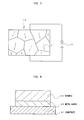
- Fig. 2 is a diagram showing spontaneous polarization of dielectric ceramic before application of an electrical field
- Fig. 3 is a diagram showing spontaneous polarization of dielectric ceramic after application of an electrical field.
- dielectric ceramic 10 having a perovskite crystal structure as shown in Fig. 2 , crystal grains 11 are spontaneously polarized in random directions, and even when a microscopic electrical field is applied in this state, distortion is offset between the crystal grains 11, and thus, no piezoelectric properties are exhibited.
- the dielectric ceramic 10 has piezoelectric properties after polarization, and when a microscopic electrical field is applied, distortion is not offset between the crystal grains 11 and the dielectric ceramic 10 is deformed.
- the microscopic electrical field does not change the directions of spontaneous polarization, and the state where the directions are uniform is maintained.
- PZT a piezoelectric constant varies depending on a direction of orientation of the dielectric ceramic film. Controlling the orientation of the PZT film is required in order to reduce a dispersion of the piezoelectric constant of the PZT film.
- the dielectric body 6 is formed as a film in accordance with an aerosol deposition method (AD method).
- the AD method is a method for film formation according to which ceramic microscopic particles are mixed with a gas and sprayed aobtainst the substrate 2 at high speed without application of heat, and thus, a strong ceramic film with high density can be fabricated, simply as a result of collision of ceramic particles.
- the ceramic particles are crushed into extremely small microscopic particles on a nano millimeter scale at the time of collision, and thus, the surface cracks at the time of collision, so that an active surface is created and bonding is caused between particles. Accordingly, the constitution of the crystal is created without sintering, and the risk of other films being negatively affected is low.
- the aerosol deposition method is appropriate for formation of a thick film.
- films of various thicknesses from thin films of several ⁇ m to thick films of several tens of ⁇ m, can be formed.
- a thick film can be formed as the piezoelectric body 6 in accordance with a gas deposition method instead of an aerosol deposition method.
- the piezoelectric body 4 may be formed as a film in accordance with various types of sputtering methods such as direct current sputtering and high-frequency sputtering, or screen printing, depending on the conditions of use.
- sputtering ceramic particles are used as a target, and an inert gas is ionized, so that the inert gas collides with the target in a vacuum, and ceramic particles separated from the target as a result of collision adhere to the substrate 2 (first metal layer 3) so that a thin film is formed.
- screen printing a screen made of a mesh and a mask is pressed against the substrate 2 (first metal layer 3) so that ceramic particles are applied to the substrate, and thus, a piezoelectric body 6 is formed.
- the film may be formed throughout the entirety on the surface of the substrate 2, as if painted solid, but appropriate changes can be made in the form, for example the pattern may be a grid or an irregular pattern, depending on the application and the state of use of the piezoelectric element 1.
- Films other than the piezoelectric body 6, such as electrodes, are formed through sputtering. Appropriate changes may be made in the form and the thickness of the film of the lower electrode 4 and the upper electrode 7, as with the piezoelectric body 6, depending on the application and the state of use of the piezoelectric element 1.
- the lower electrode 4 may lead out from an end portion of the piezoelectric element 1 or lead out from the center portion.
- the present embodiment there is a second metal layer 5 made of a metal that is easily oxidized between the piezoelectric body 6 and the lower electrode 4. Therefore, even in the case where the piezoelectric body 6 is a thick film, bonding accelerates between the piezoelectric body 6 and the lower electrode 4 through oxidation, so that the piezoelectric body 6 and the lower electrode 4 adhere naturally and firmly. Thus, there is less peeling of the piezoelectric element 1, thereby a piezoelectric element 1 having high performance can be obtained. Furthermore, because expensive Pt is not used for the lower electrode 4 and the upper electrode 7, the cost of the piezoelectric element 1 lowers.
- the metal used for the first metal layer 3 and the second metal layer 5 is a metal that is oxidized more easily (a metal having a higher ionization tendency) than the metal used for the lower electrode 4.
- a metal that is oxidized more easily (a metal having a higher ionization tendency) than the lower electrode 4 is used for the first metal layer 3 and the secondmetal layer 5
- bonds are created between the substrate 2 and the first metal layer 3, between the first metal layer 3 and the lower electrode 4, between the lower electrode 4 and the second metal layer 5, and between the second metal layer 5 and the piezoelectric body 6 through oxidation, so that the substrate 2 and the lower electrode 4, as well as the lower electrode 4 and the piezoelectric body 6, adhere firmly.
- Fig. 4 is a diagram showing a substrate on which crystalline ceramic is formed as a film according to a second embodiment of the present invention.
- a metal layer 22 is provided between a substrate 21 and ceramic 23.
- the substrate 21 is made of, for example, Si or SiO 2 , and as the ceramic 23, crystalline ceramic, for example PZT having a perovskite structure, as described above, barium titanate or a magnetic substance such as of ferrite, is used.
- Ti which is a metal that is easily oxidized
- Ti is used for the metal layer 22 between the substrate 21 and the ceramic 23. Since a metal that is easily oxidized, that is to say, a metal having a high ionization tendency, is formed as a film between the substrate 21 and the ceramic 23, adhesion can be secured between the substrate 21 and the metal layer 22, and also bonding accelerates between the metal layer 22 and the ceramic 23 through oxidation. Consequently, the metal layer 22 and the ceramic 23, thus the substrate 21 and the ceramic 23, adhere naturally and firmly.
- An oxide of Ti or an alloy of Ti can also be used for the metal layer 22.
- the metal used for the metal layer 22 may be any metal from among metals of which the ionization tendency is not less than that of Cu, oxides of metals of which the ionization tendency is not less than that of Cu, and alloys of metals of which the ionization tendency is not less than that of Cu.
- Ni which is a metal having higher ionization tendency
- an oxide of Ni or an alloy of Ni is desirable
- a metal of which the ionization tendency is not less than that of Cr, an oxide of metals of which the ionization tendency is not less than that of Cr, or an alloy of metals of which the ionization tendency is not less than that of Cr is more desirable.
- the ceramic 23 can be formed as a thick film in accordance with an aerosol deposition method or a gas deposition method, and strong adhesion in the present embodiment can be effectively used.
- the metal layer 22 is formed by sputtering.
- the ceramic 23 may be formed as a film in accordance with a screen printing method or a sputtering method. Appropriate changes can, of course, be made in the form and structure of the above-described ceramic and the like, depending on the conditions and the application etc.
Landscapes
- Engineering & Computer Science (AREA)
- Manufacturing & Machinery (AREA)
- Physical Vapour Deposition (AREA)
- Other Surface Treatments For Metallic Materials (AREA)
- Piezo-Electric Or Mechanical Vibrators, Or Delay Or Filter Circuits (AREA)
Abstract
Description
- The present invention relates to a piezoelectric element having high adhesiveness and a film formation method for crystalline ceramic.
- There are many products where piezoelectric ceramic is applied, such as piezoelectric actuators serving as a mechanical drive source utilizing the inverse piezoelectric phenomenon of piezoelectric ceramic, ceramic filters utilizing resonance, and transducers. In piezoelectric ceramic, a dielectric body having a perovskite crystal structure is used.
For example, piezoelectric actuators are excellent in terms of precision of displacement, generative force and speed of response, and multilayer piezoelectric actuators are used for X-Y tables in semiconductor manufacturing apparatuses, precision processing, printer heads and optical devices etc. - Japanese Laid-Open Patent Publication No.
2002-185285
The metal TiOx film is formed in accordance with any of a vacuum deposition method, a magnetron sputtering method and a laser ablation method, so that the metal TiOx film is changed in sequence in the direction of the film thickness by carrying out heat treatment in an oxygen atmosphere or in normal atmosphere after formation of a metal Ti film. - Japanese Laid-Open Patent Publication No.
5 (1993)-214525 - Japanese Laid-Open Patent Publication No.
5 (1993)-214526 5 (1993)-214525 - Japanese Laid-Open Patent Publication No.
8 (1996) -157213 - In the piezoelectric thin film resonator described in Japanese Laid-Open Patent Publication No.
2002-185285
In addition, though a piezoelectric thin film is formed between the electrodes, further increase in the adhesiveness is desired, in order to form a thick film. - In accordance with the method for manufacturing a cathode target described in Japanese Laid-Open Patent Publication No.
5 (1993)-214525 - In accordance with the method for manufacturing a cathode target described in Japanese Laid-Open Patent Publication No.
5 (1993)-214526 - In the oxide superconductor described in Japanese Laid-OpenPatentPublicationNo.
8 (1996)-157213 - In view of the above-described situation, an object of the present invention is to provide a piezoelectric element where strong adhesiveness can be obtained between the piezoelectric ceramic and the substrate, irrespectively of whether the piezoelectric ceramic is a thin film or a thick film, as well as a film formation method for crystalline ceramic.
- In order to achieve the above-described obj ect, the present invention provides the following technical means.
The present invention provides a piezoelectric element having a substrate, a lower electrode layered on this substrate, a piezoelectric body made of ceramic layered on top of this lower electrode, and an upper electrode layered on this piezoelectric body, wherein a first metal layer is provided between the substrate and the lower electrode, a second metal layer is provided between the lower electrode and the piezoelectric body, and the first metal layer and the second metal layer are made of a metal selected from among metals of which the ionization tendency is not less than that of Cu, oxides of metals of which the ionization tendency is not less than that of Cu, and alloys of metals of which the ionization tendency is not less than that of Cu.
In this configuration, since the second metal layer is formed of a metal of which the ionization tendency is high, that is to say, a metal that is easily oxidized, for example Cu, Cr, A1 or Ti, between the lower electrode and the piezoelectric body, oxygen bonding accelerates between the second metal layer and the piezoelectric body made of ceramic, and thus, the lower electrode and the piezoelectric body adhere naturally and firmly. Similarly, the first metal layer is provided between the lower electrode and the substrate, and thus the adhesion between the lower electrode and the substrate improves. - In the piezoelectric element according to the present invention, the first metal layer and the second metal layer may be made of a metal selected from among Ni, metals of which the ionization tendency is not less than that of Cr, oxides of Ni, oxides of metals of which the ionization tendency is not less than that of Cr, alloys of Ni, and alloys of metals of which the ionization tendency is not less than that of Cr.
In this configuration, since a metal having a particularly high ionization tendency, that is to say, a metal that is particularly easily oxidized, for example Ti, Cr or Ni, is used for the second metal layer, oxygen bonding accelerates between the secondmetal layer and the piezoelectric bodymade of ceramic, and thus, the lower electrode and the piezoelectric body adhere naturally and firmly. Similarly, the first metal layer is provided between the lower electrode and the substrate, and thus the adhesion between the lower electrode and the substrate improves. - In the piezoelectric element according to the present invention, it is preferable for the piezoelectric body to be formed as a film in accordance with any film forming method from among an aerosol deposition method, a gas deposition method, a screen printing method and a sputtering method.
The aerosol depositionmethod and the gas depositionmethod are appropriate for forming a thick film. In addition, the adhesion between the substrate and the piezoelectric ceramic is strong owing to the second metal layer made of a metal which is easily oxidized, even when the piezoelectric ceramic is a thick film, and thus, there is less peeling of the piezoelectric body. Furthermore, the adhesion between the substrate and the piezoelectric ceramic is strong even when the piezoelectric body is formed as a film in accordance with a screen printing method or a sputtering method, and the yield can be increased. - The film formation method for ceramic according to the present invention is a film formation method for crystalline ceramic according to which a metal layer is layered on a substrate and crystalline ceramic is layered on the metal layer, and the metal layer is made of a metal selected from among metals of which the ionization tendency is not less than that of Cu, oxides of metals of which the ionization tendency is not less than that of Cu, and alloys of metals of which the ionization tendency is not less than that of Cu.
According to this film formation method, since a metal layer is formed of a metal having a high ionization tendency, that is to say, a metal that is easily oxidized, for example Cu, Cr, Al or Ti, between the substrate and the crystalline ceramic, adhesion can be secured between the metal layer and the substrate, and oxygen bonding accelerates between the metal and the crystalline ceramic, and thus the substrate and the crystalline ceramic adhere naturally and firmly. - In accordance with the film formation method for crystalline ceramic according to the present invention, the metal layer may be made of a metal selected from among Ni, metals of which the ionization tendency is not less than that of Cr, oxides of Ni, oxides of metals of which the ionization tendency is not less than that of Cr, alloys of Ni, and alloys of metals of which the ionization tendency is not less than that of Cr.
In accordance with this film formation method, since a metal layer is formed of a metal having a particularly high ionization tendency, that is to say, a metal that is particularly easily oxidized, for example Ti, Cr or Ni, between the substrate and the crystalline ceramic, adhesion can be secured between the metal layer and the substrate, and oxygen bonding accelerates between the metal and the crystalline ceramic, and thus, the substrate and the crystalline ceramic adhere naturally and firmly. - In accordance with the film formation method for crystalline ceramic according to the present invention, it is preferable for the crystalline ceramic to be formed as a film in accordance with any film formation method from among an aerosol deposition method, a gas deposition method, a screen printing method and a sputtering method.
Even when a thick film is formed in accordance with an aerosol deposition method or a gas deposition method, the adhesion between the substrate and the crystalline ceramic is strong, because the metal layer is formed of a metal having a high ionization tendency, that is to say, a metal which is easily oxidized, for example Ti, Cr or Ni. In addition, though the crystalline ceramic may peel when a thin film is formed in accordance with a screen printing method or a sputtering method, the adhesion improves when a metal layer is formed of a metal which is easily oxidized, for example Ti or Cr, between the substrate and the crystalline ceramic, as described above. - According to the present invention, a piezoelectric element where the adhesion between the piezoelectric ceramic and the substrate is strong, irrespectively of whether the piezoelectric ceramic is a thin film or a thick film, as well as a film formation method for crystalline ceramic, can be obtained.
-
-
Fig. 1 is a diagram showing a piezoelectric element according to a first embodiment; -
Fig. 2 is a diagram showing spontaneous polarization in dielectric ceramic before application of an electrical field; -
Fig. 3 is a diagram showing spontaneous polarization in dielectric ceramic after application of an electrical field; and -
Fig. 4 is a diagram showing a substrate where ceramic is formed as a film according to a second embodiment. - In the following, embodiments of the present invention are described in reference to the drawings.
-
Fig. 1 is a diagram showing a piezoelectric element according to a first embodiment of the present invention. - Furthermore, a
second metal layer 5 is provided between thelower electrode 4 and apiezoelectric body 6. Thesecond metal layer 5 is also made of Ti. Since Ti has a high ionization tendency and is easily oxidized, bonding is accelerated between thesecond metal layer 5 and thepiezoelectric body 6 through oxidation, and thus thesecondmetal layer 5 and thepiezoelectric body 6 adhere naturally and firmly. - As described above, the metal used for the
first metal layer 3 and thesecond metal layer 5 is a metal that is easily oxidized, that is to say, a metal having a high ionization tendency. Concretely, this metal having a high ionization tendency is a metal of which the ionization tendency is not less than that of Cu, an oxide of a metal of which the ionization tendency is not less than that of Cu, or an alloy of a metal of which the ionization tendency is not less than that of Cu. In this case, Ni, which is a metal having a higher ionization tendency, an oxide of Ni or an alloy of Ni is desirable, and a metal of which the ionization tendency is not less than that of Cr, an oxide of a metal of which the ionization tendency is not less than that of Cr, or an alloy of a metal of which the ionization tendency is not less than that of Cr is more desirable. - Furthermore, an
upper electrode 7 is formed as a film in a layer above thepiezoelectric body 6, so that thepiezoelectric body 6 is sandwiched between theupper electrode 7 and thelower electrode 4.
Thepiezoelectric body 6 has positive piezoelectric effects where charge is generated in the crystal by applying force or causing distortion, and inverse piezoelectric effects where force or distortion is generated when an electrical field is applied to the crystal. Therefore, thepiezoelectric element 1 can be used as an actuator by applying a voltage across theelectrodes electrodes - As the
piezoelectric body 6, PZT (lead zirconate titanate, Pb(Zi, Ti)O3), for example, which is piezoelectric ceramic, is used. PZT is a ferroelectric substance having a perovskite crystal structure which can be represented by a general composition formula ABO3, and is widely used as a piezoelectric material for actuators and sensors etc. In addition, in the case where PZT isusedasathin film, it can also be used for nonvolatile memories, piezoelectric devices and optical devices. - As the
piezoelectric body 6, barium titanate (BaTiO3) can be used. Barium titanate also has a perovskite crystal structure.
In addition to the above, lead titanate (PbTiO3), PLZT (lead lanthanum zirconate titanate, (Pb, La) (Zr, Ti)O3) where a small amount of La is added to PZT and the like can be used as piezoelectric ceramic having a perovskite crystal structure. - A1, for example, is used for the electrodes i.e. the
upper electrode 7 and thelower electrode 4. Since expensive Pt is not used for theupper electrode 7 and thelower electrode 4, the cost can be reduced. In place of A1, Cu, for example, can be used. Since Cu is also less expensive than Pt, the cost can be reduced. - The
piezoelectric body 6 provides piezoelectric properties when a polarization process is carried out on a dielectric body.
Fig. 2 is a diagram showing spontaneous polarization of dielectric ceramic before application of an electrical field, andFig. 3 is a diagram showing spontaneous polarization of dielectric ceramic after application of an electrical field.
In general, in dielectric ceramic 10 having a perovskite crystal structure, as shown inFig. 2 , crystal grains 11 are spontaneously polarized in random directions, and even when a microscopic electrical field is applied in this state, distortion is offset between the crystal grains 11, and thus, no piezoelectric properties are exhibited. - As shown in
Fig. 3 , however, when a polarization process (poling) is carried out by applying an intense direct current electrical field 12 of several kv/mm, the directions of spontaneous polarization become uniform. Thus, even when the direct current electrical field 12 is removed from the polarized dielectric ceramic 10, the state where the directions of spontaneous polarization of crystal grains 11 are uniform is maintained. - The dielectric ceramic 10 has piezoelectric properties after polarization, and when a microscopic electrical field is applied, distortion is not offset between the crystal grains 11 and the dielectric ceramic 10 is deformed. Here, the microscopic electrical field does not change the directions of spontaneous polarization, and the state where the directions are uniform is maintained.
In PZT, a piezoelectric constant varies depending on a direction of orientation of the dielectric ceramic film. Controlling the orientation of the PZT film is required in order to reduce a dispersion of the piezoelectric constant of the PZT film. - Therefore, self-oriented Pt where the directions of the crystal easily become uniform is conventionally used for the
lower electrode 4 and theupper electrode 7. In the present embodiment, however, the directions of the crystal become sufficiently uniform and excellent piezoelectric properties can be obtained by carrying out a polarization process as described above, and thus the cost can be lowered by not using expensive Pt. - The
dielectric body 6 is formed as a film in accordance with an aerosol deposition method (AD method). The AD method is a method for film formation according to which ceramic microscopic particles are mixed with a gas and sprayed aobtainst thesubstrate 2 at high speed without application of heat, and thus, a strong ceramic film with high density can be fabricated, simply as a result of collision of ceramic particles.
The ceramic particles are crushed into extremely small microscopic particles on a nano millimeter scale at the time of collision, and thus, the surface cracks at the time of collision, so that an active surface is created and bonding is caused between particles.
Accordingly, the constitution of the crystal is created without sintering, and the risk of other films being negatively affected is low. - Furthermore, the aerosol deposition method is appropriate for formation of a thick film. As described above, according to the present embodiment, adhesion between the
substrate 2 and thelower electrode 4, as well as that between thelower electrode 4 and thepiezoelectric body 6, respectively increases. Thus, by using this advantage effectively, films of various thicknesses, from thin films of several µm to thick films of several tens of µm, can be formed.
Here, a thick film can be formed as thepiezoelectric body 6 in accordance with a gas deposition method instead of an aerosol deposition method. - In addition, the
piezoelectric body 4 may be formed as a film in accordance with various types of sputtering methods such as direct current sputtering and high-frequency sputtering, or screen printing, depending on the conditions of use.
In sputtering, ceramic particles are used as a target, and an inert gas is ionized, so that the inert gas collides with the target in a vacuum, and ceramic particles separated from the target as a result of collision adhere to the substrate 2 (first metal layer 3) so that a thin film is formed.
In screen printing, a screen made of a mesh and a mask is pressed against the substrate 2 (first metal layer 3) so that ceramic particles are applied to the substrate, and thus, apiezoelectric body 6 is formed. - As for the pattern of the
piezoelectric body 6 formed as a film, the film may be formed throughout the entirety on the surface of thesubstrate 2, as if painted solid, but appropriate changes can be made in the form, for example the pattern may be a grid or an irregular pattern, depending on the application and the state of use of thepiezoelectric element 1. - Films other than the
piezoelectric body 6, such as electrodes, are formed through sputtering.
Appropriate changes may be made in the form and the thickness of the film of thelower electrode 4 and theupper electrode 7, as with thepiezoelectric body 6, depending on the application and the state of use of thepiezoelectric element 1. Thelower electrode 4 may lead out from an end portion of thepiezoelectric element 1 or lead out from the center portion. - As described above, according to the present embodiment, there is a
second metal layer 5 made of a metal that is easily oxidized between thepiezoelectric body 6 and thelower electrode 4. Therefore, even in the case where thepiezoelectric body 6 is a thick film, bonding accelerates between thepiezoelectric body 6 and thelower electrode 4 through oxidation, so that thepiezoelectric body 6 and thelower electrode 4 adhere naturally and firmly. Thus, there is less peeling of thepiezoelectric element 1, thereby apiezoelectric element 1 having high performance can be obtained.
Furthermore, because expensive Pt is not used for thelower electrode 4 and theupper electrode 7, the cost of thepiezoelectric element 1 lowers. Here, the metal used for thefirst metal layer 3 and thesecond metal layer 5 is a metal that is oxidized more easily (a metal having a higher ionization tendency) than the metal used for thelower electrode 4. When a metal that is oxidized more easily (a metal having a higher ionization tendency) than thelower electrode 4 is used for thefirst metal layer 3 and thesecondmetal layer 5, bonds are created between thesubstrate 2 and thefirst metal layer 3, between thefirst metal layer 3 and thelower electrode 4, between thelower electrode 4 and thesecond metal layer 5, and between thesecond metal layer 5 and thepiezoelectric body 6 through oxidation, so that thesubstrate 2 and thelower electrode 4, as well as thelower electrode 4 and thepiezoelectric body 6, adhere firmly. -
Fig. 4 is a diagram showing a substrate on which crystalline ceramic is formed as a film according to a second embodiment of the present invention.
As shown inFig. 4 , in the second embodiment, ametal layer 22 is provided between asubstrate 21 andceramic 23.
Thesubstrate 21 is made of, for example, Si or SiO2, and as the ceramic 23, crystalline ceramic, for example PZT having a perovskite structure, as described above, barium titanate or a magnetic substance such as of ferrite, is used. - In addition, Ti, which is a metal that is easily oxidized, is used for the
metal layer 22 between thesubstrate 21 and the ceramic 23.
Since a metal that is easily oxidized, that is to say, a metal having a high ionization tendency, is formed as a film between thesubstrate 21 and the ceramic 23, adhesion can be secured between thesubstrate 21 and themetal layer 22, and also bonding accelerates between themetal layer 22 and the ceramic 23 through oxidation. Consequently, themetal layer 22 and the ceramic 23, thus thesubstrate 21 and the ceramic 23, adhere naturally and firmly.
An oxide of Ti or an alloy of Ti can also be used for themetal layer 22. When such a metal is used, bonding accelerates between themetal layer 22 and the ceramic 23 through oxidation, so that themetal layer 22 and the ceramic 23, thus thesubstrate 21 and the ceramic 23, adhere naturally and firmly. The metal used for themetal layer 22 may be any metal from among metals of which the ionization tendency is not less than that of Cu, oxides of metals of which the ionization tendency is not less than that of Cu, and alloys of metals of which the ionization tendency is not less than that of Cu. In this case, Ni, which is a metal having higher ionization tendency, an oxide of Ni or an alloy of Ni is desirable, and a metal of which the ionization tendency is not less than that of Cr, an oxide of metals of which the ionization tendency is not less than that of Cr, or an alloy of metals of which the ionization tendency is not less than that of Cr is more desirable. - The ceramic 23 can be formed as a thick film in accordance with an aerosol deposition method or a gas deposition method, and strong adhesion in the present embodiment can be effectively used. The
metal layer 22 is formed by sputtering. The ceramic 23 may be formed as a film in accordance with a screen printing method or a sputtering method.
Appropriate changes can, of course, be made in the form and structure of the above-described ceramic and the like, depending on the conditions and the application etc.
Claims (6)
- A piezoelectric element, comprising: a substrate; a lower electrode layered on said substrate; a piezoelectric body made of ceramic layered on top of said lower electrode; and an upper electrode layered on said piezoelectric body, whereina first metal layer is provided between said substrate and said lower electrode,a second metal layer is provided between said lower electrode and said piezoelectric body, andsaid first metal layer and said second metal layer are made of a metal selected from among metals of which the ionization tendency is not less than that of Cu, oxides of metals of which the ionization tendency is not less than that of Cu and alloys of metals of which the ionization tendency is not less than that of Cu.
- The piezoelectric element according to claim 1, whereinsaid first metal layer and said second metal layer are made of a metal selected from among Ni, metals of which the ionization tendency is not less than that of Cr, oxides of Ni, oxides of metals of which the ionization tendency is not less than that of Cr, alloys of Ni, and alloys of metals of which the ionization tendency is not less than that of Cr.
- The piezoelectric element according to claim 1 or 2, whereinsaid piezoelectric body is formed as a film in accordance with any film formation method from among an aerosol deposition method, a gas deposition method, a screen printing method and a sputtering method.
- A film formation method for crystalline ceramic according to which a metal layer is layered on a substrate and crystalline ceramic is layered on said metal layer, whereinsaid metal layer is made of a metal selected from among metals of which the ionization tendency is not less than that of Cu, oxides of metals of which the ionization tendency is not less than that of Cu, and alloys of metals of which the ionization tendency is not less than that of Cu.
- The film formation method for crystalline ceramic according to claim 4, whereinsaid metal layer is made of a metal selected from among Ni, metals of which the ionization tendency is not less than that of Cr, oxides of Ni, oxides of metals of which the ionization tendency is not less than that of Cr, alloys of Ni, and alloys of metals of which the ionization tendency is not less than that of Cr.
- The film formation method for crystalline ceramic according to claim 4 or 5, whereinsaid crystalline ceramic is formed as a film in accordance with any film formation method from among an aerosol deposition method, a gas deposition method, a screen printing method and a sputtering method.
Applications Claiming Priority (1)
| Application Number | Priority Date | Filing Date | Title |
|---|---|---|---|
| JP2007101405A JP2008258516A (en) | 2007-04-09 | 2007-04-09 | Piezoelectric element and crystalline ceramic film forming method |
Publications (2)
| Publication Number | Publication Date |
|---|---|
| EP1981098A2 true EP1981098A2 (en) | 2008-10-15 |
| EP1981098A3 EP1981098A3 (en) | 2012-08-08 |
Family
ID=39600970
Family Applications (1)
| Application Number | Title | Priority Date | Filing Date |
|---|---|---|---|
| EP20080006982 Withdrawn EP1981098A3 (en) | 2007-04-09 | 2008-04-08 | Piezoelectric element and film formation method for crystalline ceramic |
Country Status (3)
| Country | Link |
|---|---|
| US (1) | US7622854B2 (en) |
| EP (1) | EP1981098A3 (en) |
| JP (1) | JP2008258516A (en) |
Families Citing this family (5)
| Publication number | Priority date | Publication date | Assignee | Title |
|---|---|---|---|---|
| JP5729065B2 (en) * | 2011-03-23 | 2015-06-03 | コニカミノルタ株式会社 | Thin film piezoelectric device |
| US8981627B2 (en) | 2012-06-04 | 2015-03-17 | Tdk Corporation | Piezoelectric device with electrode films and electroconductive oxide film |
| US20130320813A1 (en) * | 2012-06-04 | 2013-12-05 | Tdk Corporation | Dielectric device |
| US9136820B2 (en) | 2012-07-31 | 2015-09-15 | Tdk Corporation | Piezoelectric device |
| US8994251B2 (en) | 2012-08-03 | 2015-03-31 | Tdk Corporation | Piezoelectric device having first and second non-metal electroconductive intermediate films |
Citations (1)
| Publication number | Priority date | Publication date | Assignee | Title |
|---|---|---|---|---|
| JP2002185285A (en) | 2000-12-08 | 2002-06-28 | Murata Mfg Co Ltd | Electrode structure of piezoelectric thin film resonator and method of forming the same |
Family Cites Families (17)
| Publication number | Priority date | Publication date | Assignee | Title |
|---|---|---|---|---|
| JPS5411173U (en) * | 1977-06-24 | 1979-01-24 | ||
| JP3651910B2 (en) | 1991-08-28 | 2005-05-25 | 旭硝子セラミックス株式会社 | Ceramic rotating cathode target and manufacturing method thereof |
| JP3651909B2 (en) | 1991-08-28 | 2005-05-25 | 旭硝子セラミックス株式会社 | Ceramic rotating cathode target and manufacturing method thereof |
| JP3195886B2 (en) | 1994-12-06 | 2001-08-06 | 三菱電機株式会社 | Oxide superconducting film and manufacturing method thereof |
| JPH09280947A (en) * | 1996-04-11 | 1997-10-31 | Matsushita Electric Ind Co Ltd | Ferroelectric element |
| JP4328854B2 (en) * | 2003-01-22 | 2009-09-09 | 独立行政法人産業技術総合研究所 | Piezoelectric element and manufacturing method thereof |
| US7262544B2 (en) * | 2004-01-09 | 2007-08-28 | Canon Kabushiki Kaisha | Dielectric element, piezoelectric element, ink jet head and method for producing the same head |
| JP4250593B2 (en) * | 2004-01-09 | 2009-04-08 | キヤノン株式会社 | Dielectric element, piezoelectric element, ink jet head, and manufacturing method thereof |
| US7265483B2 (en) * | 2004-03-29 | 2007-09-04 | Canon Kabushiki Kaisha | Dielectric member, piezoelectric member, ink jet head, ink jet recording apparatus and producing method for ink jet recording apparatus |
| US7235917B2 (en) * | 2004-08-10 | 2007-06-26 | Canon Kabushiki Kaisha | Piezoelectric member element and liquid discharge head comprising element thereof |
| JP4016983B2 (en) * | 2004-12-07 | 2007-12-05 | 株式会社村田製作所 | Piezoelectric thin film resonator and manufacturing method thereof |
| JP4697517B2 (en) * | 2004-12-16 | 2011-06-08 | 株式会社村田製作所 | Piezoelectric thin film resonator and manufacturing method thereof |
| JP4344942B2 (en) * | 2004-12-28 | 2009-10-14 | セイコーエプソン株式会社 | Inkjet recording head and piezoelectric actuator |
| JP2006245248A (en) * | 2005-03-02 | 2006-09-14 | Seiko Epson Corp | Piezoelectric element and manufacturing method thereof, liquid ejecting head and manufacturing method thereof, and liquid ejecting apparatus |
| CN101137596B (en) * | 2005-03-08 | 2011-05-25 | 日本碍子株式会社 | Piezoelectric/electrostrictive ceramic composition and manufacturing method thereof |
| JP5087824B2 (en) * | 2005-07-25 | 2012-12-05 | 富士ゼロックス株式会社 | Piezoelectric element, droplet discharge head, and droplet discharge apparatus |
| JP5241087B2 (en) * | 2005-08-23 | 2013-07-17 | キヤノン株式会社 | Piezoelectric body, piezoelectric element, liquid discharge head using the piezoelectric element, liquid discharge apparatus, and method for manufacturing the piezoelectric element |
-
2007
- 2007-04-09 JP JP2007101405A patent/JP2008258516A/en active Pending
-
2008
- 2008-04-08 US US12/099,519 patent/US7622854B2/en not_active Expired - Fee Related
- 2008-04-08 EP EP20080006982 patent/EP1981098A3/en not_active Withdrawn
Patent Citations (1)
| Publication number | Priority date | Publication date | Assignee | Title |
|---|---|---|---|---|
| JP2002185285A (en) | 2000-12-08 | 2002-06-28 | Murata Mfg Co Ltd | Electrode structure of piezoelectric thin film resonator and method of forming the same |
Also Published As
| Publication number | Publication date |
|---|---|
| US20080248324A1 (en) | 2008-10-09 |
| JP2008258516A (en) | 2008-10-23 |
| US7622854B2 (en) | 2009-11-24 |
| EP1981098A3 (en) | 2012-08-08 |
Similar Documents
| Publication | Publication Date | Title |
|---|---|---|
| JP5044902B2 (en) | Piezoelectric thin film element | |
| CN101355134B (en) | Piezoelectric element, inkjet head, angular velocity sensor and manufacturing method thereof, inkjet type recording device | |
| EP0667646B1 (en) | Piezoelectric/electrostrictive film element and method of producing the same | |
| EP0526048B1 (en) | Piezoelectric/electrostrictive element having ceramic substrate formed essentially of stabilized zirconia | |
| JP6091281B2 (en) | Piezoelectric thin film multilayer substrate | |
| CN112750941B (en) | Piezoelectric thin film element | |
| US7622854B2 (en) | Piezoelectric element and film formation method for crystalline ceramic | |
| JP7588007B2 (en) | Piezoelectric thin film, piezoelectric thin film element, and piezoelectric transducer | |
| JP6196797B2 (en) | Piezoelectric thin film multilayer substrate and piezoelectric thin film element | |
| EP4694657A1 (en) | Piezoelectric multilayer body, method for producing piezoelectric multilayer body, and piezoelectric element | |
| US7348711B2 (en) | Piezoelectric/electrostrictive element, method of manufacturing piezoelectric/electrostrictive element, piezoelectric/electrostrictive device, and method of manufacturing piezoelectric/electrostrictive device | |
| JP3282085B2 (en) | Method for manufacturing piezoelectric / electrostrictive film element | |
| JP3999473B2 (en) | Integral piezoelectric / electrostrictive membrane element having excellent durability and method for manufacturing the same | |
| JP3126212B2 (en) | Piezoelectric / electrostrictive film type element | |
| JP2010118447A (en) | Piezoelectric film type element | |
| US10388851B2 (en) | Piezoelectric element | |
| CN111384229B (en) | Film laminate, film element, and laminate substrate | |
| JP2001156351A (en) | Laminated electrode, method of forming the same, and piezoelectric actuator | |
| JP5121186B2 (en) | Piezoelectric body, piezoelectric element, liquid discharge head, and liquid discharge apparatus | |
| JP3272004B2 (en) | Piezoelectric / electrostrictive film type element | |
| JP6804615B2 (en) | A method for manufacturing a laminated substrate having a piezoelectric film, an element having a piezoelectric film, and a laminated substrate having a piezoelectric film. | |
| EP4694656A1 (en) | Piezoelectric multilayer body, method for producing piezoelectric multilayer body, and piezoelectric element | |
| JP7579109B2 (en) | Piezoelectric thin film, piezoelectric thin film element, and piezoelectric transducer | |
| JP2011129774A (en) | Method of manufacturing substrate with piezoelectric thin film | |
| CN120225032A (en) | Device having piezoelectric element, laminated substrate, and method for manufacturing the device |
Legal Events
| Date | Code | Title | Description |
|---|---|---|---|
| PUAI | Public reference made under article 153(3) epc to a published international application that has entered the european phase |
Free format text: ORIGINAL CODE: 0009012 |
|
| AK | Designated contracting states |
Kind code of ref document: A2 Designated state(s): AT BE BG CH CY CZ DE DK EE ES FI FR GB GR HR HU IE IS IT LI LT LU LV MC MT NL NO PL PT RO SE SI SK TR |
|
| AX | Request for extension of the european patent |
Extension state: AL BA MK RS |
|
| PUAL | Search report despatched |
Free format text: ORIGINAL CODE: 0009013 |
|
| AK | Designated contracting states |
Kind code of ref document: A3 Designated state(s): AT BE BG CH CY CZ DE DK EE ES FI FR GB GR HR HU IE IS IT LI LT LU LV MC MT NL NO PL PT RO SE SI SK TR |
|
| AX | Request for extension of the european patent |
Extension state: AL BA MK RS |
|
| RIC1 | Information provided on ipc code assigned before grant |
Ipc: H01L 41/24 20060101ALI20120704BHEP Ipc: H01L 41/09 20060101AFI20120704BHEP Ipc: H01L 41/047 20060101ALI20120704BHEP |
|
| AKY | No designation fees paid | ||
| REG | Reference to a national code |
Ref country code: DE Ref legal event code: R108 |
|
| REG | Reference to a national code |
Ref country code: DE Ref legal event code: R108 Effective date: 20130417 |
|
| STAA | Information on the status of an ep patent application or granted ep patent |
Free format text: STATUS: THE APPLICATION IS DEEMED TO BE WITHDRAWN |
|
| 18D | Application deemed to be withdrawn |
Effective date: 20130209 |