EP1976013A2 - Solid-state imaging device and driving method thereof - Google Patents
Solid-state imaging device and driving method thereof Download PDFInfo
- Publication number
- EP1976013A2 EP1976013A2 EP08005125A EP08005125A EP1976013A2 EP 1976013 A2 EP1976013 A2 EP 1976013A2 EP 08005125 A EP08005125 A EP 08005125A EP 08005125 A EP08005125 A EP 08005125A EP 1976013 A2 EP1976013 A2 EP 1976013A2
- Authority
- EP
- European Patent Office
- Prior art keywords
- pixel
- voltage
- state
- heat conduction
- semiconductor substrate
- Prior art date
- Legal status (The legal status is an assumption and is not a legal conclusion. Google has not performed a legal analysis and makes no representation as to the accuracy of the status listed.)
- Withdrawn
Links
Images







Classifications
-
- H—ELECTRICITY
- H10—SEMICONDUCTOR DEVICES; ELECTRIC SOLID-STATE DEVICES NOT OTHERWISE PROVIDED FOR
- H10F—INORGANIC SEMICONDUCTOR DEVICES SENSITIVE TO INFRARED RADIATION, LIGHT, ELECTROMAGNETIC RADIATION OF SHORTER WAVELENGTH OR CORPUSCULAR RADIATION
- H10F39/00—Integrated devices, or assemblies of multiple devices, comprising at least one element covered by group H10F30/00, e.g. radiation detectors comprising photodiode arrays
- H10F39/10—Integrated devices
- H10F39/12—Image sensors
- H10F39/18—Complementary metal-oxide-semiconductor [CMOS] image sensors; Photodiode array image sensors
- H10F39/184—Infrared image sensors
-
- G—PHYSICS
- G01—MEASURING; TESTING
- G01J—MEASUREMENT OF INTENSITY, VELOCITY, SPECTRAL CONTENT, POLARISATION, PHASE OR PULSE CHARACTERISTICS OF INFRARED, VISIBLE OR ULTRAVIOLET LIGHT; COLORIMETRY; RADIATION PYROMETRY
- G01J5/00—Radiation pyrometry, e.g. infrared or optical thermometry
- G01J5/02—Constructional details
- G01J5/0225—Shape of the cavity itself or of elements contained in or suspended over the cavity
- G01J5/0245—Shape of the cavity itself or of elements contained in or suspended over the cavity for performing thermal shunt
-
- G—PHYSICS
- G01—MEASURING; TESTING
- G01J—MEASUREMENT OF INTENSITY, VELOCITY, SPECTRAL CONTENT, POLARISATION, PHASE OR PULSE CHARACTERISTICS OF INFRARED, VISIBLE OR ULTRAVIOLET LIGHT; COLORIMETRY; RADIATION PYROMETRY
- G01J5/00—Radiation pyrometry, e.g. infrared or optical thermometry
- G01J5/10—Radiation pyrometry, e.g. infrared or optical thermometry using electric radiation detectors
- G01J5/20—Radiation pyrometry, e.g. infrared or optical thermometry using electric radiation detectors using resistors, thermistors or semiconductors sensitive to radiation, e.g. photoconductive devices
Definitions
- the present invention relates to a solid-state imaging device and driving a solid-state imaging device, for example, an uncooled-type solid-state imaging element detecting a light having a long wave length.
- An image sensor detecting a light ray in bands of wavelengths of 8 to 12 micrometers ( ⁇ m) including an infrared band, a terahertz band, a millimeter-wave band, and the like has high sensitivity to a light ray emitted from an object having a temperature near room temperature. Accordingly, such an image sensor has been applied to a security camera, an on-vehicle forward-looking camera or the like.
- MEMS Micro-Electro-Mechanical System
- the uncooled-type optical sensor irradiates a light ray condensed by, for example, a far-infrared lens (Ge lens) onto each of pixels and converts heat generated by the light ray into an electric signal.
- the uncooled-type optical sensor generates an image based on the generated electric signal.
- the uncooled-type optical sensor of this type needs to detect the light ray in a state in which the pixels are thermally separated from a semiconductor substrate. Because each of the pixels is continuously heated by the light ray, it is difficult for the conventional uncooled-type optical sensor to detect an electric signal in a dark state (a state in which light is not incident on each pixel).
- thermoelectric conversion A signal voltage obtained by the thermoelectric conversion is low as compared with a voltage of the electric signal (i.e., a bias component) in the dark state.
- a voltage of the electric signal i.e., a bias component
- bias components cannot be eliminated from the respective pixels for the above-stated reason. Due to this, at the time of starting the sensor with the lens covered with a lens cover, the signal in the dark state (a fixed pattern) output from each pixel is stored in a frame memory in advance. Thereafter, the fixed pattern is subtracted from the detected electric signal corresponding to each pixel, thereby outputting signal components corresponding to an incident light.
- JP-A 2004-085331 discloses a thermal-type infrared image pickup device provided with including a mechanical switch so as to be able to quickly respond to an infrared ray.
- This mechanical switch causes rapid thermal conduction between a cell part and a semiconductor substrate in a period in which no electric signals are detected from respective pixels, and thermally separates the cell part from the semiconductor substrate in a signal detection period.
- the thermal-type infrared imaging device disclosed therein can, therefore, pick up an image at high speed.
- the thermal-type infrared imaging device disclosed therein is unable to read signals output from the respective pixels in a state in which the cell part is shorted to the semiconductor substrate, that is, in a thermally reset state. As a result, 1/f noise and irregularities in fixed pattern among the pixels cannot be eliminated.
- An advantage of an aspect of the present invention is to provide a solid-state imaging device which can execute a thermal reset operation and which can eliminate 1/f noise and irregularities in fixed pattern.
- a solid-state imaging device comprises a semiconductor substrate; a pixel converting a heat energy generated by an incident light into an electric signal, the pixel being supported on a cavity formed in the semiconductor substrate and being thermally separated from the semiconductor substrate; a heat conduction switch having one end connected to the semiconductor substrate and other end capable of contacting to the semiconductor substrate or the pixel, the heat conduction switch changing over a state of the pixel to one of a first state and a second state, the first state being a state in which the pixel is thermally isolated from the semiconductor substrate by causing the other end of the heat conduction switch to contact with the semiconductor substrate, the second state being a state in which the pixel is thermally shorted to the semiconductor substrate by causing the other end of the heat conduction switch to contact with the pixel; and a signal detector detecting a difference between the signal voltage of the pixel in the first state and the signal voltage of the pixel in the second state.
- a method of driving a solid-state imaging device including a semiconductor substrate; a pixel converting a heat energy generated by an incident light into an electric signal, the pixel being supported on a cavity formed in the semiconductor substrate and thermally separated from the semiconductor substrate; a signal line transmitting a signal voltage output from the pixel; a heat conduction switch having one end connected to the semiconductor substrate and other end capable of contacting to the semiconductor substrate or the pixel; and a signal detector capacitively coupled to the signal line
- the method comprises detecting a difference between the signal voltage of the pixel in a first state and the signal voltage of the pixel in a second state, the first state being a state in which the pixel is thermally isolated from the semiconductor substrate by causing the other end of the heat conduction switch to contact with the semiconductor substrate, the second state being a state in which the pixel is thermally shorted to the semiconductor substrate by causing the other end of the heat conduction switch to contact with the pixel.
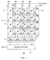
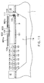
- a thermal-type sensor 100 (hereinafter, "sensor 100") shown in Fig. 1 is, for example, a long-wavelength sensor such as an infrared sensor, a terahertz sensor or a millimeter-wave sensor.
- the infrared sensor 100 is provided with an imaging region 10 that includes 16 pixels 3 arranged in a matrix (four rows by four columns) on a semiconductor substrate. Although the imaging region 10 generally includes more pixels, the number of pixels is set to 16 for the sake of convenience in the first embodiment.
- Each of the pixels 3 in the imaging region 10 includes a pn junction (diode) 4.
- Each pixel 3 converts heat energy generated by an incident light into an electric signal. More specifically, a signal is read by applying forward current to the pn junction 4 and reading a voltage according to an operating point that changes by a temperature of the pn junction 4.
- the temperature change of the pn junction 4 is about 5 ⁇ 10 -3 of that of an object. Namely, if the temperature of the object changes by 1 Kelvin (K), a pixel temperature changes by 5 millikelvins (mK). If eight silicon pn junctions are connected in series, thermoelectric conversion efficiency is about 10 mV/K. Therefore, if the temperature of the object changes by 1 K, a signal voltage of 50 microvolts ( ⁇ V) is generated in each pixel 3. Actually, it is often required to discriminate the temperature change of about 0.1 K of the object. To meet the requirement, the sensor 100 needs to read a signal voltage as low as, for example, 5 ⁇ V generated in each pixel 3.
- Row selection lines 5 are connected to the pixels 3 arranged in a row direction.
- Vertical signal lines (hereinafter, also “signal lines”) 6 are connected to the pixels 3 arranged in a column direction.
- Each of the row selection lines 5 is connected to one end (an anode side) of the pn junction 4 of each pixel 3 whereas each of the signal lines 6 is connected to the other end (a cathode side) thereof.
- the row selection lines 5 are connected to a vertical scanner 50.
- the vertical scanner 50 applies a pulse voltage to a selected row selection line 5.
- the signal lines 6 are provided to correspond to the respective pixel columns, and each of the signal lines 6 is connected between the pixels 3 arranged in the column direction and each of constant current sources 60.
- the constant current sources 60 are configured to apply a constant current to the respective pixels 3 in the imaging region 10.
- Heat conduction switches SW are provided to correspond to the respective pixels 3.
- the heat conduction switches SW are configured to be able to contact with either the semiconductor substrate or the corresponding pixels 3.
- the imaging region 10 turns into a first state in which the imaging region 10 is thermally isolated from the semiconductor substrate.
- the heat conduction switches SW can selectively change over the state of the imaging region 10 between the first state and the second state.
- Signal detectors 7 are provided to correspond to the respective signal lines 6.
- the signal detectors 7 have an input 70 for performing a clamping operation, and start the clamping operation in response to a clamp pulse.
- Each of the signal detectors 7 detects the column voltage Vsl transmitted from the corresponding signal line 6.
- Each of the signal lines 6 functions to transmit the signal voltage generated in the pixels 3 to the corresponding signal detector 7.
- the signal detectors 7 are connected to a horizontal read circuit 11.
- the horizontal read circuit 11 sequentially outputs signals detected by the signal detectors 7 to an outside of the sensor 100.
- Fig. 2 is a plan view of the pixel 3.
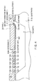
- Fig. 4 is a cross-sectional view taken along a line 4-4 of Fig. 2 .
- a cavity 4 is formed in a silicon substrate 1.
- the pixel 3 is supported on the cavity 14 by a support unit 12.
- the cavity 14 is formed by etching a surface of the silicon substrate 1.
- the pixel 3 is formed simultaneously with formation of the cavity 14 by protecting a surface region of the silicon substrate 1.
- the support unit 12 is formed likely to the pixel 3. Accordingly, the pixel 3 and the support unit 12 are made of silicon.
- the support unit 12 is formed on the same layer equal in height level as that on which the pixel 3 is formed based on the surface of the silicon substrate 1.
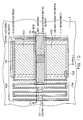
- One heat conduction switch SW is provided between the pixel 3 and the silicon substrate 1 (between the pixel 3 and a portion thermally shorted to the silicon substrate 1). As shown in Fig. 2 , the heat conduction switch SW is configured so that one end is connected to the silicon substrate 1 and the other end is connected to either the silicon substrate 1 or the pixel 3. Similarly to the pixel 3 and the support unit 12, the heat conduction switch SW is formed simultaneously with the formation of the cavity 14. Further, the heat conduction switch SW is formed on the same layer equal in height level as that on which the pixel 3 and the support unit 12 are formed based on the surface of the silicon substrate 1. The heat conduction switch SW is adjacent to the pixel 3 and formed into, for example, a cantilever made of silicon.
- An interconnect 111 is formed in the heat conduction switch SW.
- the interconnect 111 is made of, for example, metal or doped silicon.
- a first electrode 13 is provided near a portion of the pixel 3 with which portion the heat conduction switch SW contacts.
- a second electrode 113 is provided near a portion of the silicon substrate 1 with which portion the heat conduction switch SW contacts.
- the first electrode 13 is connected to one of the row selection lines 5 shown in Fig. 1 via a terminal 151 and an interconnect 12A.
- the second electrode 113 is connected to a circuit (not shown) formed on the silicon substrate 1.
- Fig. 2 shows a state in which the heat conduction switch SW is in contact with the pixel 3.
- the state shown in Fig. 2 corresponds to the second state.
- Fig. 3 shows a state in which the heat conduction switch SW is in contact with the portion thermally shorted to the silicon substrate 1.
- the state shown in Fig. 3 corresponds to the first state.
- the support unit 12 electrically connects the silicon substrate 1 to the pixel 3 and also mechanically supports the pixel 3. Normally, the sensor 100 is actuated in vacuum, so that the heat generated in the pixel 3 is diffused only from the support unit 12. Nevertheless, the support unit 12 is formed in zigzags so as to thermally separate the pixel 3 from the silicon substrate 1. By forming the support unit 12 longer and thinner, the pixel 3 can be further thermally isolated from the silicon substrate 1.
- the support unit 12 includes interconnects 12A and 12B.
- the pixel 3 includes a thermoelectric conversion element configured to include an anode 161 and a cathode 162 forming the pn junction 4 shown in Fig. 1 .
- the terminal 151 connected to the anode 161 is connected to one row selection line 5 shown in Fig. 1 via the interconnect 12A.
- the pulse voltage from the vertical scanner 50 can be thereby transmitted to the anode 161.
- the constant current from the vertical scanner 50 can be supplied to the anode 161.
- a terminal 153 connected to the cathode 162 is connected to one signal line 6 shown in Fig. 1 via the interconnect 12B.
- the corresponding constant-current source 60 can thereby carry the constant current to the cathode 162.
- the corresponding signal detector 7 can detect the signal voltage generated in the pixel 3 via the signal line 6.
- a bias voltage Vdd is applied to the first electrode 13 via the row selection line 5 or the like, and at the same time, a switch voltage Vsw of the interconnect 111 is set to be equal to the bias voltage Vdd.
- a potential of the second electrode 113 is set to a ground potential GND.
- a potential difference Vdd is generated between the interconnect 111 and the second electrode 113.
- a force F1 generated between the heat conduction switch SW and the silicon substrate 1 due to this potential difference Vdd is represented by the following Equation (1).
- Equation (1) if the interconnect 111 and the second electrode 113 are assumed as polar plates of a capacitor, respectively, symbols ⁇ , d, and S denote a dielectric constant of a material (including a vacuum) between the interconnect 111 and the second electrode 113, a distance between the interconnect 111 and the second electrode 113, and an area by which the interconnect 111 is opposed to the second electrode 113, respectively.
- the force F1 is an attraction force which attracts the interconnect 111 and the second electrode 113 to each other.
- the heat conduction switch SW is bent in the direction of the silicon substrate 1 side and contacts with the silicon substrate 1. As a result, the sensor 100 turns into the first state.
- the bias voltage Vdd is applied to the first electrode 13 and the potential Vsw of the interconnect 111 is set to the ground potential GND while the potential of the second electrode 113 is set to the ground potential GND.
- the potential difference Vdd is generated between the interconnect 111 and the first electrode 13.
- a force F2 generated between the heat conduction switch SW and the pixel 3 due to this potential difference Vdd is represented by the following Equation (2).
- the force F2 is an attraction force which attracts the interconnect 111 and the first electrode 13 to each other.
- the heat conduction switch SW is bent in the direction of the pixel 3 side and contacts with the pixel 3. As a result, the sensor 100 turns into the second state.
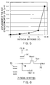
- the heat conduction switch SW is structured so that a silicon oxide film having a thickness of 0.1 ⁇ m is coated onto surroundings of polysilicon having a thickness of 0.5 ⁇ m and a width of 0.5 ⁇ m. It is also assumed that a gap between the heat conduction switch SW and a side surface of the pixel 3 is 0.7 ⁇ m. In this case, as obvious from Fig. 5 , the heat conduction switch SW contacts with the pixel 3 when the potential difference between the heat conduction switch SW and the pixel 3 is about 18 V.
- Fig. 6 is a circuit diagram of each of the signal detectors 7.
- the signal detector 7 is also referred to as "correlation double sampling circuit".
- the signal detector 7 includes a first node N, a coupling capacitor CC, a clamping transistor Tcl, a storage capacitor SC, and an output terminal OUT.
- a terminal 71 is connected to one signal line 6.
- the coupling capacitor CC capacitively couples the first node N to the signal line 6.
- a terminal 70 is connected to a clamping voltage source that supplies the constant voltage Vcl.
- the clamping transistor Tcl is connected between the first node N and the clamping voltage source.
- the transistor Tcl is controlled to be turned on or off according to a gate voltage Vgcl.
- the storage capacitor SC is connected between the first node N and the ground potential GND, and keeps a reference potential by storing therein charges during a clamping operation.
- the output terminal OUT outputs a voltage detected at the first node N.
- Fig. 7 is a circuit diagram of the horizontal read circuit 11.
- the horizontal read circuit 11 includes horizontal selection transistors 120, a read line 130, a horizontal shift register 140, a source follower circuit 150 serving as a buffer circuit, and a read reset switch 160.
- Each of the horizontal selection transistors 120 is connected between the read line 130 and each of the signal detectors 7.
- the horizontal shift register 140 is connected to gates of the respective horizontal selection transistors 120.
- the horizontal shift register 140 sequentially transmits signals output from the signal detectors 7 to the read line 130 by sequentially turning on the horizontal selection transistors 120.
- the output signals from the signal detectors 7 are output from the read line 130 to the outside of the sensor 100 via the source follower circuit 150.
- the read reset switch 160 is provided to reset the read line 130 to the bias voltage Vdd after the signal output from a certain signal line 6 is read.
- the source follower circuit 150 functions as a buffer circuit.
- An inverter amplifier circuit may be employed as the buffer circuit in place of the source follower circuit 150.
- the imaging region 10 absorbs an incident light and the temperature of the imaging region 10 rises.
- the bias voltage Vdd is applied to the pn junctions 4 of the pixels 3 via the row selection lines 5.
- the voltage Vsw of the interconnect 111 of each of the heat conduction switches SW is raised to Vdd.
- a voltage V13 of the first electrode 13 rises to Vdd.
- a voltage V113 of the second electrode 113 remains the ground potential GND.
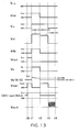
- the potential difference Vdd is generated between the interconnect 111 and the second electrode 113, thereby turning the sensor 100 into the first state. Namely, in the period between t1 and t2, each pixel 3 is in the state in which the pixel 3 is thermally isolated from the silicon substrate 1.
- the voltage Vsl of each signal line 6 is (Vdd-Vd0+dVsh+dV).
- Vd0 denotes a voltage applied to the pn junction 4 in the dark state.
- dVsh denotes a self-heating voltage component generated at the pn junction 4 by pulse voltages V13 to V43 (see Fig. 8 ) applied from the vertical scanner 50 shown in Fig. 1 .
- Symbol dV denotes a signal voltage component generated by the incident light. Namely, if the heat is not generated in each pixel 3 by the incident light (in case of the dark state), the voltage Vsl of each signal line 6 is (Vdd-Vd0+dVsh).
- the voltage Vsl is (Vdd-Vd0+dVsh+dV) obtained by adding bias components (Vdd-Vd0+dVsh) to the signal voltage component dV resulting from the incident light.
- a signal voltage ⁇ V resulting from the incident light is considered and represented as follows.
- the temperature of each pixel 3 is raised by ⁇ T, which is represented by the following Equation (3), by heat energy generated by the incident light.
- ⁇ ⁇ T P a G th 1 - exp ( - t ⁇ G th / C th
- Gth denotes a heat conductance of the support unit 12
- Pa denotes an energy amount of Joule heat generated in each pixel 3
- t denotes passing time since start of reception of electric signals
- Cth denotes a heat capacity of the pixel 3.
- the temperature rise (self-heating temperature component) ⁇ T of the pixel 3 nears a value represented by the following Equation (4) in a stationary state (t ⁇ ).
- ⁇ ⁇ T P a G th
- the temperature rise ⁇ T of the pixel 3 due to the incident light is decided only by the energy amount of the incident light and the heat conductance of the support unit 12 in the stationary state.
- the thermoelectric conversion efficiency is represented by dV/dT. Therefore, in the stationary state, the pixel 3 outputs a voltage dV represented by the Equation (5).
- the voltage dV corresponds to the signal voltage component resulting from the incident light.
- the self-heating voltage component dVsh is a voltage generated by self heating (a self-heating temperature component) ⁇ Tsh represented by the following Equation (6).
- ⁇ ⁇ Tsh Vd ⁇ 0 * If Gth ⁇ 1 - exp - tGth / Gth
- Equation (6) symbol "If” denotes a forward current carried across the diode (pn junction) 4 and t denotes passing time since a current starts to be applied to the diode (pn junction) 4.
- the self-heating temperature component ⁇ Tsh will be described later with reference to Fig. 9 .
- the charges stored in the storage capacitor SC are held during an operation in a next period from t2 to t3, whereby the potential Vn of the first node N is kept equal to the clamping voltage Vcl in the period between t2 and t3. Accordingly, in the period between t2 and t3, the clamping voltage Vcl serves as the reference potential.
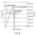
- the self-heating temperature component ⁇ Tsh and the signal temperature component ⁇ T resulting from the incident light change as shown in Fig. 9 .
- the self-heating temperature component ⁇ Tsh and the signal temperature component ⁇ T are temperature components for the pixel 3 based on the temperature of the silicon substrate 1, respectively.
- the signal temperature component ⁇ T In the period between t1 and t2 (in the first state), the signal temperature component ⁇ T is steady state shown in the Equation (4).
- the signal temperature component ⁇ T is almost constant to, for example, 8 ⁇ 10 -3 K.
- the self-heating temperature component ⁇ T rises because a current is carried across each pn junction 4 at the rise of the pulse voltage (e.g., V13).
- the voltage Vsl of each signal line 6 is (Vdd-Vd0+dVsh). This is because the heat generated by the incident light is diffused from each pixel 3 to the silicon substrate 1 since the pixel 3 is thermally shorted to the silicon substrate 1. In other words, the pixel 3 turns into the dark state.
- the self-heating temperature component ⁇ Tsh is not zero. That is, the self-heating voltage component dVsh is not zero.
- the heat conduction switch SW contacts with each pixel 3.
- the signal temperature component ⁇ T and the self-heating temperature component ⁇ Tsh are diffused to the silicon substrate 1 from each pixel 3 via the heat conduction switch SW. Accordingly, the signal temperature component ⁇ T is almost zero whereas the self-heating temperature component ⁇ Tsh is, for example, about 0.1 K for the following reason.
- the pulse voltage is not lowered yet. Due to this, the self-heating temperature component ⁇ Tsh continues to be generated while being diffused to the silicon substrate 1.
- the gate voltage Vgcl shown in Fig. 6 falls to the ground potential GND and the clamping transistor Tcl is turned off. Accordingly, the charges of the first node N are held, and the potential Vn of the first node N falls from the reference voltage Vcl by as much as a voltage (dV'+dVsh') proportional to the signal voltage component ⁇ V and the self-heating voltage component dVsh (dV+dVsh). Namely, the voltage Vn of the first node N is equal to a second voltage (Vcl-dV'-dVsh').
- the voltage (dV'+dVsh') is equal to 1/2*(dV+dVsh).
- the self-heating voltage component dVsh is a constant voltage and far lower than the bias component (Vdd-Vd0). Further, the self-heating voltage component dVsh has no change among frames and hardly has irregularities among the pixels 3.
- the voltage Vcl is a preset constant voltage, it is possible to easily extract the signal voltage component dV' of the incident light from the second voltage (Vcl-dV'-dVsh').
- the horizontal read circuit 11 serially reads voltages Vn in all columns. Therefore, as the voltage Vout shown in Fig. 8 , signals as many as columns appear in the period between t3 and t4.
- the signal voltage component dV' is obtained from (Vcl-dV') without consideration to the bias component (Vdd-Vd0) as already stated. Since the signal voltage component dV' does not depend on the bias component (Vdd-Vd0), the irregularities in fixed pattern among the pixels 3 and the influence of the 1/f noise can be eliminated.
- the sensor 100 according to the first embodiment can thereby improve an S/N ratio (signal-to-noise ratio). Moreover, since the irregularities in fixed pattern among the pixels 3 and the influence of the 1/f noise are not present, there is no need to provide an elimination circuit for eliminating them. Therefore, the sensor 100 according to the first embodiment can be advantageously made small in size and manufactured at low cost.
- the bias component (Vdd-Vd0) is irregular among the pixels 3. If a signal is a faint signal having the signal voltage component dV, for example, equal to or lower than 1 mV, the bias component (Vdd-Vd0) has often an irregularity of about several tens of millivolts among the pixels 3. In this case, the bias component (Vdd-Vd0) is output as a fixed pattern greater than the signal voltage component dV' by one digit. According to the first embodiment, the signal voltage component dV' can be detected without influence of the irregularities in bias component (Vdd-Vd0).
- signals in the bright state (t1 to t2) and signals in the dark state (t3 to t4) are chopped off at high frequency. It is, therefore, possible to greatly eliminate the 1/f noise.
- one pixel 3 includes one pn junction 4.
- one pixel 3 may be configured to include a diode string in which a plurality of pn junctions (diodes) is connected in series.
- a pixel 3 according to a second embodiment of the present invention includes an antenna 901 receiving an electromagnetic wave and converting the electromagnetic wave into an electric signal, and a resistance heating element 902 converting the electric signal generated in the antenna 901 into Joule heat and raising a temperature of the pixel 3.
- the remaining constituent elements of the second embodiment can be the same as those according to the first embodiment.
- the antenna 901 which is made of a metal film having a quite low electric resistance, receives an incident electric wave.
- the resistance of the antenna 901 is preferably as low as, for example, 10 ⁇ .
- a length of the antenna 901 is preferably about half the wavelength of the electric wave to be received. By so configuring, the antenna 901 can selectively receive the electric wave at a long wavelength as stated above.
- the antenna 901 is divided into, for example, a first antenna unit 901a and a second antenna unit 901b.
- the first antenna unit 901a and the second antenna unit 901b are electrically connected to the resistance heating element 902.
- the resistance heating element 902 has a resistance of, for example, about 200 ⁇ .
- the resistance heating element 902 and the antenna 901 are electrically separated from the thermoelectric conversion element (including the anode 161 and the cathode 162) provided on a lower layer, they are thermally integrated with the thermoelectric conversion element.
- the antenna 901 and the resistance heating element 902 are coated with an antenna protection film 903.
- the antenna protection film 903 functions to protect the antenna 901 and the resistance heating element 902 from an etching solution used during the formation of the cavity 14.
- An electromagnetic wave to be processed by a solid-state image pickup device 1 according to the second embodiment is present in a quite high frequency range from a gigahertz band to a terahertz band. It is difficult to convert the electromagnetic wave into an electric signal and to detect the electric signal. Considering these, each pixel 3 according to the second embodiment converts the Joule heat generated when a current produced by the electromagnetic wave passes through the resistance heating element 902 into an electric signal.
- the Joule heat Pa is represented by the following Equation (7).
- Pa I ⁇ a 2 * Ra
- Ia denotes the current generated by the electromagnetic wave and Ra denotes the resistance value of the resistance heating element 902.
- a faint signal output from each pixel 3 is amplified and a difference between a bright-state signal and a dark-state signal is output.
- a column amplifier including an amplifier transistor Tamp, nodes N10 to N12, a coupling capacitor CC, a feedback transistor Tfb, a storage capacitor SC, a selection transistor Tsel, and a reset transistor Trs is employed as a signal detector 7 according to the third embodiment, as shown in Fig. 12 .
- the node N11 is connected to a drain of the amplifier transistor Tamp.
- the node N10 is connected to a gate of the amplifier transistor Tamp.
- the coupling capacitor CC is connected between the node N10 and one signal line 6, and capacitively couples the gate of the amplifier transistor Tamp to the signal line 6.
- the feedback transistor Tfb is connected between the nodes N11 and N10, and connects the gate of the amplifier transistor Tamp to the drain thereof during a clamping operation. By doing so, the feedback transistor Tfb holds threshold voltage information on the amplifier transistor Tamp in the gate of the amplifier transistor Tamp.
- the selection transistor Tsel is connected between the nodes N11 and N12.
- the selection transistor Tsel transmits a reset voltage Vrs to the node N11 during the clamping operation, and transmits a potential of the node N11 to the node N12 during a read operation.
- the storage capacitor SC is connected between the node N12 and a reference voltage (ground), and stores therein charges carried across the amplifier transistor Tamp via the selection transistor Tsel. If the amplifier transistor Tamp is an N-MOSFET, the charges stored in the storage capacitor SC are electrons.
- the reset transistor Trs is connected between the node N12 and the reset voltage Vrs, and turned on during a reset operation for setting potentials of the nodes N12 and N11 to the reset voltage Vrs.
- the reset transistor Trs is turned on, the potential of the storage capacitor SC is reset to the reset voltage Vrs.
- the node N12 is present between the reset transistor Trs and the selection transistor Tsel, and serves as an output node CDS-out connected to the horizontal read circuit 11.
- the third embodiment differs from the first and second embodiments in the configuration of the signal detector 7.
- the remaining constituent elements of the third embodiment can be the same as those according to the first or second embodiment.
- Fig. 13 is a timing chart showing an operation performed by a sensor according to the third embodiment.
- the storage capacitor SC is reset. More specifically, a gate voltage Vrst of the reset transistor Trs and a gate voltage Vsel of the selection transistor Tsel are raised by a pulse voltage. A voltage of the storage capacitor SC and a drain voltage of the amplifier transistor Tamp are thereby set to the reset voltage Vrs. In other words, the potentials of the nodes N11 and N12 become equal to the reset voltage Vrs.
- the potential of the signal line 6 is (Vdd-V0+dVsh+dV) similarly to the first embodiment.
- the transistor Tamp is, therefore, turned on.
- a gate voltage Vfb of the feedback transistor Tfb is raised by the pulse voltage to thereby turn on the feedback transistor Tfb.
- a source potential Vs of the amplifier transistor Tamp is raised to satisfy Vs>0.
- the selection transistor Tsel is turned off.
- the source voltage Vs is connected to the node N10 via the transistors Tamp and Tfb. Accordingly, as shown in Fig.
- a potential Vg of the node N10 is closer to the drain voltage Vrs of the amplifier transistor Tamp in the initial period. Thereafter, however, current is carried from the node N10 to the node N11 via the feedback transistor Tfb. As a result, the gate voltage Vg of the amplifier transistor Tamp (the voltage Vg of the node N10) is closer to a clamping voltage (Vs+Vth).
- the gate voltage Vfb of the feedback transistor Tfb is set to zero V to thereby turn off the feedback transistor Tfb.
- the heat conduction switch SW changes over the state of the imaging region 10 to the second state. Due to this, a potential Vsl of the signal line 6 is changed to (Vdd-Vd0).
- the gate voltage Vg of the amplifier transistor Tamp (the voltage Vg of the node N10) is lower than the clamping voltage (Vs+Vth) by (dVsh+dV). As a result, current corresponding to the voltage (Vs+Vth-dVsh-dV) is carried from the storage capacitor SC toward the node N11.
- An amount of current carried at that moment corresponds to a voltage drop of the storage capacitor SC. Furthermore, the voltage (Vs+Vth-dVsh-dV) is output from the output node CDS-out to the horizontal read circuit 11 and read by the horizontal read circuit 11.
- the signal voltage resulting from the incident light can be amplified, integrated, and output without irregularities in fixed pattern among the pixels 3 and the influence of the 1/f noise.
- the heat conduction switch SW has a stacked structure long in the vertical direction to the surface of the silicon substrate 1. More specifically, the heat conduction switch SW includes a polysilicon layer 111a, and one or more metal layers are formed on the polysilicon layer 111a. In Fig. 15 , two metal layers 111c and 111e are deposited on the polysilicon layer 111a. To make potentials of the metal layers 111c and 111e and the polysilicon layer 111a equal, contacts 111b and 111d are connected to the metal layers 111c and 111e, respectively.
- the first electrode 13 includes a polysilicon layer 13a and one or more metal layers are formed on the polysilicon layer 13a.
- two metal layers 13c and 13e are deposited on the polysilicon layer 13a.
- contacts 13b and 13d are connected to the metal layers 13c and 13e, respectively.
- the second electrode 113 includes a polysilicon layer 113a, and one or more metal layers are formed on the polysilicon layer 113a.
- two metal layers 113c and 113e are deposited on the polysilicon layer 113a.
- contacts 113b and 113d are connected to the metal layers 113c and 113e, respectively.
- a root 115 of the heat conduction switch SW is preferably structured so that the polysilicon layer 111a of a single layer structure is covered with a silicon oxide film.
- a stacked portion 114 is assumed as a tip end of the heat conduction switch SW.
- Each of the first electrode 13 and the second electrode 113 includes a stacked structure long in the vertical direction to the surface of the silicon substrate 1 in a portion opposed to the stacked portion 114 of the heat conduction switch SW. It is thereby possible to increase an area S by which the heat conduction switch SW is opposed to the first electrode 13 and an area S by which the heat conduction switch SW is opposed to the second electrode 113.
- a force F3 acting on the stacked portion 114 per unit length is represented by the following Equation (8).
- F ⁇ 3 1 / 2 * ⁇ * ( VSw / d ) * 2 ⁇ 3 ⁇ S
- the force F3 is three times as high as that acting on the heat conduction switch SW constituted only by the polysilicon layer.
- the heat conduction switch SW according to the fourth embodiment can be driven at lower voltage by increasing the area of the portion of the heat conduction switch SW on which portion the electrostatic force acts.
- the fourth embodiment can be combined with any of the first to third embodiments. By such combinations, further, the fourth embodiment can obtain effects of the first to third embodiments.
Landscapes
- Physics & Mathematics (AREA)
- General Physics & Mathematics (AREA)
- Spectroscopy & Molecular Physics (AREA)
- Solid State Image Pick-Up Elements (AREA)
- Transforming Light Signals Into Electric Signals (AREA)
- Radiation Pyrometers (AREA)
Abstract
Description
- The present invention relates to a solid-state imaging device and driving a solid-state imaging device, for example, an uncooled-type solid-state imaging element detecting a light having a long wave length.
- An image sensor detecting a light ray in bands of wavelengths of 8 to 12 micrometers (µm) including an infrared band, a terahertz band, a millimeter-wave band, and the like has high sensitivity to a light ray emitted from an object having a temperature near room temperature. Accordingly, such an image sensor has been applied to a security camera, an on-vehicle forward-looking camera or the like. In recent years, following development of MEMS (Micro-Electro-Mechanical System) process, a thermal-type optical sensor (an uncooled-type optical sensor) sensing a light ray without cooling an element has become popular as an image sensor.
- The uncooled-type optical sensor irradiates a light ray condensed by, for example, a far-infrared lens (Ge lens) onto each of pixels and converts heat generated by the light ray into an electric signal. The uncooled-type optical sensor generates an image based on the generated electric signal. The uncooled-type optical sensor of this type needs to detect the light ray in a state in which the pixels are thermally separated from a semiconductor substrate. Because each of the pixels is continuously heated by the light ray, it is difficult for the conventional uncooled-type optical sensor to detect an electric signal in a dark state (a state in which light is not incident on each pixel). A signal voltage obtained by the thermoelectric conversion is low as compared with a voltage of the electric signal (i.e., a bias component) in the dark state. However, in the uncooled-type sensor, bias components cannot be eliminated from the respective pixels for the above-stated reason. Due to this, at the time of starting the sensor with the lens covered with a lens cover, the signal in the dark state (a fixed pattern) output from each pixel is stored in a frame memory in advance. Thereafter, the fixed pattern is subtracted from the detected electric signal corresponding to each pixel, thereby outputting signal components corresponding to an incident light.
- In this case, however, it is necessary to additionally provide a circuit for subtracting the fixed pattern from each electric signal, disadvantageously resulting in an increase in a size of the sensor. Furthermore, if the fixed pattern has temporal change, then an initial fixed pattern cannot be used and it is disadvantageously necessary to regularly update the fixed pattern.
-
JP-A 2004-085331 - An advantage of an aspect of the present invention is to provide a solid-state imaging device which can execute a thermal reset operation and which can eliminate 1/f noise and irregularities in fixed pattern.
- A solid-state imaging device according to an embodiment of the present invention comprises a semiconductor substrate; a pixel converting a heat energy generated by an incident light into an electric signal, the pixel being supported on a cavity formed in the semiconductor substrate and being thermally separated from the semiconductor substrate; a heat conduction switch having one end connected to the semiconductor substrate and other end capable of contacting to the semiconductor substrate or the pixel, the heat conduction switch changing over a state of the pixel to one of a first state and a second state, the first state being a state in which the pixel is thermally isolated from the semiconductor substrate by causing the other end of the heat conduction switch to contact with the semiconductor substrate, the second state being a state in which the pixel is thermally shorted to the semiconductor substrate by causing the other end of the heat conduction switch to contact with the pixel; and a signal detector detecting a difference between the signal voltage of the pixel in the first state and the signal voltage of the pixel in the second state.
- A method of driving a solid-state imaging device according to an embodiment of the present invention, the device including a semiconductor substrate; a pixel converting a heat energy generated by an incident light into an electric signal, the pixel being supported on a cavity formed in the semiconductor substrate and thermally separated from the semiconductor substrate; a signal line transmitting a signal voltage output from the pixel; a heat conduction switch having one end connected to the semiconductor substrate and other end capable of contacting to the semiconductor substrate or the pixel; and a signal detector capacitively coupled to the signal line,
the method comprises detecting a difference between the signal voltage of the pixel in a first state and the signal voltage of the pixel in a second state, the first state being a state in which the pixel is thermally isolated from the semiconductor substrate by causing the other end of the heat conduction switch to contact with the semiconductor substrate, the second state being a state in which the pixel is thermally shorted to the semiconductor substrate by causing the other end of the heat conduction switch to contact with the pixel. -
-
Fig. 1 is a schematic diagram of a thermal-type sensor 100 according to a first embodiment; -
Fig. 2 is a plane view of thepixel 3 in a first state; -
Fig. 3 is a plane view of thepixel 3 in a second state; -
Fig. 4 is a cross-sectional view taken along a line 4-4 ofFig. 2 ; , -
Fig. 5 is a graph showing a displacement of a heat conduction switch; -
Fig. 6 is a circuit diagram of thesignal detectors 7; -
Fig. 7 is a circuit diagram of thehorizontal read circuit 11; -
Fig. 8 is a timing chart showing an operation of thesensor 100; -
Fig. 9 is a graph showing the signal component ΔT and the self-heating temperature component ΔTsh; -
Fig. 10 is a plane view of the pixel according to a second embodiment; -
Fig. 11 is a cross-sectional view taken along a line 11-11 ofFig. 10 ; -
Fig. 12 is a circuit diagram of thecolumn amplifier 7; -
Fig. 13 is a timing chart showing an operation performed by a sensor according to the third embodiment; -
Fig. 14 is a plane view of thepixel 3 according to a fourth embodiment; and -
Fig. 15 is a cross-sectional view taken along a line 15-15 ofFig. 14 . - Embodiments of the present invention will be explained below with reference to the accompanying drawings. The present invention is not limited to the embodiments.
- A thermal-type sensor 100 (hereinafter, "
sensor 100") shown inFig. 1 is, for example, a long-wavelength sensor such as an infrared sensor, a terahertz sensor or a millimeter-wave sensor. Theinfrared sensor 100 is provided with animaging region 10 that includes 16pixels 3 arranged in a matrix (four rows by four columns) on a semiconductor substrate. Although theimaging region 10 generally includes more pixels, the number of pixels is set to 16 for the sake of convenience in the first embodiment. Each of thepixels 3 in theimaging region 10 includes a pn junction (diode) 4. Eachpixel 3 converts heat energy generated by an incident light into an electric signal. More specifically, a signal is read by applying forward current to thepn junction 4 and reading a voltage according to an operating point that changes by a temperature of thepn junction 4. - Generally, while the temperature change of the
pn junction 4 depends on absorptance of an infrared absorbing layer or an optical system, the temperature change of thepn junction 4 is about 5×10⁻³ of that of an object. Namely, if the temperature of the object changes by 1 Kelvin (K), a pixel temperature changes by 5 millikelvins (mK). If eight silicon pn junctions are connected in series, thermoelectric conversion efficiency is about 10 mV/K. Therefore, if the temperature of the object changes by 1 K, a signal voltage of 50 microvolts (µV) is generated in eachpixel 3. Actually, it is often required to discriminate the temperature change of about 0.1 K of the object. To meet the requirement, thesensor 100 needs to read a signal voltage as low as, for example, 5 µV generated in eachpixel 3. -
Row selection lines 5 are connected to thepixels 3 arranged in a row direction. Vertical signal lines (hereinafter, also "signal lines") 6 are connected to thepixels 3 arranged in a column direction. Each of therow selection lines 5 is connected to one end (an anode side) of thepn junction 4 of eachpixel 3 whereas each of thesignal lines 6 is connected to the other end (a cathode side) thereof. - The
row selection lines 5 are connected to avertical scanner 50. Thevertical scanner 50 applies a pulse voltage to a selectedrow selection line 5. Thesignal lines 6 are provided to correspond to the respective pixel columns, and each of thesignal lines 6 is connected between thepixels 3 arranged in the column direction and each of constantcurrent sources 60. The constantcurrent sources 60 are configured to apply a constant current to therespective pixels 3 in theimaging region 10. When thevertical scanner 50 applies a pulse voltage to thepn junctions 4 in a selected row, thepn junctions 4 in the selected row are biased in forward direction. As a result, a column voltage Vsl is generated on the signal lines 6. On the other hand, thepn junctions 4 in unselected rows are all biased in reverse direction, so that the unselectedrow selection lines 5 are separated from the signal lines 6. - Heat conduction switches SW are provided to correspond to the
respective pixels 3. The heat conduction switches SW are configured to be able to contact with either the semiconductor substrate or the correspondingpixels 3. By causing the heat conduction switches SW to contact with the semiconductor substrate, theimaging region 10 turns into a first state in which theimaging region 10 is thermally isolated from the semiconductor substrate. By causing the heat conduction switches SW to contact with thepn junctions 4, theimaging region 10 turns into a second state in which thepn junctions 4 are thermally shorted to the semiconductor substrate. The heat conduction switches SW can selectively change over the state of theimaging region 10 between the first state and the second state. -
Signal detectors 7 are provided to correspond to therespective signal lines 6. Thesignal detectors 7 have aninput 70 for performing a clamping operation, and start the clamping operation in response to a clamp pulse. Each of thesignal detectors 7 detects the column voltage Vsl transmitted from thecorresponding signal line 6. Each of thesignal lines 6 functions to transmit the signal voltage generated in thepixels 3 to thecorresponding signal detector 7. - The
signal detectors 7 are connected to ahorizontal read circuit 11. Thehorizontal read circuit 11 sequentially outputs signals detected by thesignal detectors 7 to an outside of thesensor 100. - A configuration of each of the
pixels 3 will be described.Fig. 2 is a plan view of thepixel 3.Fig. 4 is a cross-sectional view taken along a line 4-4 ofFig. 2 . As shown inFig. 4 , acavity 4 is formed in asilicon substrate 1. Thepixel 3 is supported on thecavity 14 by asupport unit 12. Thecavity 14 is formed by etching a surface of thesilicon substrate 1. Thepixel 3 is formed simultaneously with formation of thecavity 14 by protecting a surface region of thesilicon substrate 1. Thesupport unit 12 is formed likely to thepixel 3. Accordingly, thepixel 3 and thesupport unit 12 are made of silicon. Thesupport unit 12 is formed on the same layer equal in height level as that on which thepixel 3 is formed based on the surface of thesilicon substrate 1. - One heat conduction switch SW is provided between the
pixel 3 and the silicon substrate 1 (between thepixel 3 and a portion thermally shorted to the silicon substrate 1). As shown inFig. 2 , the heat conduction switch SW is configured so that one end is connected to thesilicon substrate 1 and the other end is connected to either thesilicon substrate 1 or thepixel 3. Similarly to thepixel 3 and thesupport unit 12, the heat conduction switch SW is formed simultaneously with the formation of thecavity 14. Further, the heat conduction switch SW is formed on the same layer equal in height level as that on which thepixel 3 and thesupport unit 12 are formed based on the surface of thesilicon substrate 1. The heat conduction switch SW is adjacent to thepixel 3 and formed into, for example, a cantilever made of silicon. - An
interconnect 111 is formed in the heat conduction switch SW. Theinterconnect 111 is made of, for example, metal or doped silicon. Afirst electrode 13 is provided near a portion of thepixel 3 with which portion the heat conduction switch SW contacts. Asecond electrode 113 is provided near a portion of thesilicon substrate 1 with which portion the heat conduction switch SW contacts. Thefirst electrode 13 is connected to one of therow selection lines 5 shown inFig. 1 via aterminal 151 and aninterconnect 12A. Thesecond electrode 113 is connected to a circuit (not shown) formed on thesilicon substrate 1. - By applying a potential to the
interconnect 111, thefirst electrode 13, and thesecond electrode 113, an attraction force is applied to the heat conduction switch SW to thereby bend the heat conduction switch SW in a direction of eitherpixel 3 side orsilicon substrate 1 side. By changing the potential of theinterconnect 111, thefirst electrode 13 or thesecond electrode 113, the heat conduction switch SW can change over the state of theimaging region 10 between the first state and the second state.Fig. 2 shows a state in which the heat conduction switch SW is in contact with thepixel 3. The state shown inFig. 2 corresponds to the second state.Fig. 3 shows a state in which the heat conduction switch SW is in contact with the portion thermally shorted to thesilicon substrate 1. The state shown inFig. 3 corresponds to the first state. - The
support unit 12 electrically connects thesilicon substrate 1 to thepixel 3 and also mechanically supports thepixel 3. Normally, thesensor 100 is actuated in vacuum, so that the heat generated in thepixel 3 is diffused only from thesupport unit 12. Nevertheless, thesupport unit 12 is formed in zigzags so as to thermally separate thepixel 3 from thesilicon substrate 1. By forming thesupport unit 12 longer and thinner, thepixel 3 can be further thermally isolated from thesilicon substrate 1. Thesupport unit 12 includesinterconnects silicon substrate 1 to thepixel 3 via theinterconnect pixel 3 to the circuit formed on thesilicon substrate 1 via theinterconnect - As shown in
Fig. 2 , thepixel 3 includes a thermoelectric conversion element configured to include ananode 161 and acathode 162 forming thepn junction 4 shown inFig. 1 . The terminal 151 connected to theanode 161 is connected to onerow selection line 5 shown inFig. 1 via theinterconnect 12A. The pulse voltage from thevertical scanner 50 can be thereby transmitted to theanode 161. Furthermore, the constant current from thevertical scanner 50 can be supplied to theanode 161. A terminal 153 connected to thecathode 162 is connected to onesignal line 6 shown inFig. 1 via theinterconnect 12B. The corresponding constant-current source 60 can thereby carry the constant current to thecathode 162. Furthermore, thecorresponding signal detector 7 can detect the signal voltage generated in thepixel 3 via thesignal line 6. - To turn the
sensor 100 into the first state, a bias voltage Vdd is applied to thefirst electrode 13 via therow selection line 5 or the like, and at the same time, a switch voltage Vsw of theinterconnect 111 is set to be equal to the bias voltage Vdd. At this time, a potential of thesecond electrode 113 is set to a ground potential GND. As a result, a potential difference Vdd is generated between theinterconnect 111 and thesecond electrode 113. A force F1 generated between the heat conduction switch SW and thesilicon substrate 1 due to this potential difference Vdd is represented by the following Equation (1).
In the Equation (1), if theinterconnect 111 and thesecond electrode 113 are assumed as polar plates of a capacitor, respectively, symbols ε, d, and S denote a dielectric constant of a material (including a vacuum) between theinterconnect 111 and thesecond electrode 113, a distance between theinterconnect 111 and thesecond electrode 113, and an area by which theinterconnect 111 is opposed to thesecond electrode 113, respectively. - The force F1 is an attraction force which attracts the
interconnect 111 and thesecond electrode 113 to each other. As shown inFig. 3 , the heat conduction switch SW is bent in the direction of thesilicon substrate 1 side and contacts with thesilicon substrate 1. As a result, thesensor 100 turns into the first state. - To turn the
sensor 100 into the second state, the bias voltage Vdd is applied to thefirst electrode 13 and the potential Vsw of theinterconnect 111 is set to the ground potential GND while the potential of thesecond electrode 113 is set to the ground potential GND. As a result, the potential difference Vdd is generated between theinterconnect 111 and thefirst electrode 13. A force F2 generated between the heat conduction switch SW and thepixel 3 due to this potential difference Vdd is represented by the following Equation (2).
In the Equation (2), if theinterconnect 111 and thefirst electrode 13 are assumed as polar plates of a capacitor, respectively, symbols ε', d', and S' denote a dielectric constant of a material (including a vacuum) between theinterconnect 111 and thefirst electrode 13, a distance between theinterconnect 111 and thefirst electrode 13, and an area by which theinterconnect 111 is opposed to thefirst electrode 13, respectively. - The force F2 is an attraction force which attracts the
interconnect 111 and thefirst electrode 13 to each other. As shown inFig. 3 , the heat conduction switch SW is bent in the direction of thepixel 3 side and contacts with thepixel 3. As a result, thesensor 100 turns into the second state. - It is assumed, for example, that the heat conduction switch SW is structured so that a silicon oxide film having a thickness of 0.1 µm is coated onto surroundings of polysilicon having a thickness of 0.5 µm and a width of 0.5 µm. It is also assumed that a gap between the heat conduction switch SW and a side surface of the
pixel 3 is 0.7 µm. In this case, as obvious fromFig. 5 , the heat conduction switch SW contacts with thepixel 3 when the potential difference between the heat conduction switch SW and thepixel 3 is about 18 V. -
Fig. 6 is a circuit diagram of each of thesignal detectors 7. Thesignal detector 7 is also referred to as "correlation double sampling circuit". Thesignal detector 7 includes a first node N, a coupling capacitor CC, a clamping transistor Tcl, a storage capacitor SC, and an output terminal OUT. A terminal 71 is connected to onesignal line 6. The coupling capacitor CC capacitively couples the first node N to thesignal line 6. A terminal 70 is connected to a clamping voltage source that supplies the constant voltage Vcl. The clamping transistor Tcl is connected between the first node N and the clamping voltage source. The transistor Tcl is controlled to be turned on or off according to a gate voltage Vgcl. The storage capacitor SC is connected between the first node N and the ground potential GND, and keeps a reference potential by storing therein charges during a clamping operation. The output terminal OUT outputs a voltage detected at the first node N. -
Fig. 7 is a circuit diagram of thehorizontal read circuit 11. Thehorizontal read circuit 11 includeshorizontal selection transistors 120, aread line 130, ahorizontal shift register 140, asource follower circuit 150 serving as a buffer circuit, and aread reset switch 160. Each of thehorizontal selection transistors 120 is connected between the readline 130 and each of thesignal detectors 7. Thehorizontal shift register 140 is connected to gates of the respectivehorizontal selection transistors 120. Thehorizontal shift register 140 sequentially transmits signals output from thesignal detectors 7 to the readline 130 by sequentially turning on thehorizontal selection transistors 120. The output signals from thesignal detectors 7 are output from the readline 130 to the outside of thesensor 100 via thesource follower circuit 150. The read resetswitch 160 is provided to reset the readline 130 to the bias voltage Vdd after the signal output from acertain signal line 6 is read. Thesource follower circuit 150 functions as a buffer circuit. An inverter amplifier circuit may be employed as the buffer circuit in place of thesource follower circuit 150. - With reference to
Fig. 8 , an operation performed by thesensor 100 according to the first embodiment will be described next. - Before t1, the
imaging region 10 absorbs an incident light and the temperature of theimaging region 10 rises. In a period between t1 and t2, the bias voltage Vdd is applied to thepn junctions 4 of thepixels 3 via the row selection lines 5. At the same time, the voltage Vsw of theinterconnect 111 of each of the heat conduction switches SW is raised to Vdd. By applying the bias voltage Vdd to therow selection lines 5, a voltage V13 of thefirst electrode 13 rises to Vdd. At this moment, a voltage V113 of thesecond electrode 113 remains the ground potential GND. As a result, the potential difference Vdd is generated between theinterconnect 111 and thesecond electrode 113, thereby turning thesensor 100 into the first state. Namely, in the period between t1 and t2, eachpixel 3 is in the state in which thepixel 3 is thermally isolated from thesilicon substrate 1. - At this time, the voltage Vsl of each
signal line 6 is (Vdd-Vd0+dVsh+dV). Symbol Vd0 denotes a voltage applied to thepn junction 4 in the dark state. Symbol dVsh denotes a self-heating voltage component generated at thepn junction 4 by pulse voltages V13 to V43 (seeFig. 8 ) applied from thevertical scanner 50 shown inFig. 1 . Symbol dV denotes a signal voltage component generated by the incident light. Namely, if the heat is not generated in eachpixel 3 by the incident light (in case of the dark state), the voltage Vsl of eachsignal line 6 is (Vdd-Vd0+dVsh). Accordingly, in the period between t1 and t2, i.e., in the first state, the voltage Vsl is (Vdd-Vd0+dVsh+dV) obtained by adding bias components (Vdd-Vd0+dVsh) to the signal voltage component dV resulting from the incident light. - A signal voltage ΔV resulting from the incident light is considered and represented as follows. The temperature of each
pixel 3 is raised by ΔT, which is represented by the following Equation (3), by heat energy generated by the incident light.
In the Equation (3), Gth denotes a heat conductance of thesupport unit 12, Pa denotes an energy amount of Joule heat generated in eachpixel 3, t denotes passing time since start of reception of electric signals, and Cth denotes a heat capacity of thepixel 3. - The temperature rise (self-heating temperature component) ΔT of the
pixel 3 nears a value represented by the following Equation (4) in a stationary state (t→∞).
- As obvious from the following Equation (4), the temperature rise ΔT of the
pixel 3 due to the incident light is decided only by the energy amount of the incident light and the heat conductance of thesupport unit 12 in the stationary state. For example, if the constant current is applied to thepn junction 4 and a change in voltages on both ends of thepn junction 4 is detected, the thermoelectric conversion efficiency is represented by dV/dT. Therefore, in the stationary state, thepixel 3 outputs a voltage dV represented by the Equation (5). The voltage dV corresponds to the signal voltage component resulting from the incident light.
- The self-heating voltage component dVsh is a voltage generated by self heating (a self-heating temperature component) ΔTsh represented by the following Equation (6).

- In the Equation (6), symbol "If" denotes a forward current carried across the diode (pn junction) 4 and t denotes passing time since a current starts to be applied to the diode (pn junction) 4. The self-heating temperature component ΔTsh will be described later with reference to
Fig. 9 . - In the period between t1 and t2, the gate voltage Vgcl shown in
Fig. 6 rises to high level potential Vrst, and the clamping transistor Tcl is turned on. Accordingly, a potential Vn of the first node N is kept equal to the clamping voltage Vcl serving as the reference voltage. At this moment, a voltage (Vcl-(Vdd-V0+dVsh+dv)) is applied to both ends of the coupling capacitor CC. Since the first node N is capacitively coupled to thesignal line 6, charges according to the Equation (5) are stored in the storage capacitor SC from the terminal 70. Such an operation between t1 and t2 is called "clamping operation". The charges stored in the storage capacitor SC are held during an operation in a next period from t2 to t3, whereby the potential Vn of the first node N is kept equal to the clamping voltage Vcl in the period between t2 and t3. Accordingly, in the period between t2 and t3, the clamping voltage Vcl serves as the reference potential. - With reference to
Fig. 9 , the self-heating temperature component ΔTsh and the signal temperature component ΔT resulting from the incident light in the period between t1 and t2 will be described below. It is assumed that the heat conductance between eachpixel 3 and thesilicon substrate 1 in the period between t1 and t2 (in the period in which the heat conduction switch SW is turned off) is Gth_leg=100 nW (nanoWatt)/K (Kelvin). Further, the heat conductance between eachpixel 3 and thesilicon substrate 1 in the period between t2 and t3 (in the period in which the heat conduction switch SW is turned on) is Gth_sw=50 µW/K. In this case, the self-heating temperature component ΔTsh and the signal temperature component ΔT resulting from the incident light change as shown inFig. 9 . The self-heating temperature component ΔTsh and the signal temperature component ΔT are temperature components for thepixel 3 based on the temperature of thesilicon substrate 1, respectively. - In the period between t1 and t2 (in the first state), the signal temperature component ΔT is steady state shown in the Equation (4). The signal temperature component ΔT is almost constant to, for example, 8×10⁻³ K. On the other hand, the self-heating temperature component ΔT rises because a current is carried across each
pn junction 4 at the rise of the pulse voltage (e.g., V13). - Referring back to
Fig. 8 , in the period between t2 and t3, while the bias voltage Vdd is kept applied to thepn junction 4, the voltage Vsw of theinterconnect 111 of each heat conduction switch SW is lowered to the ground potential GND. As a result, the potential difference Vdd is generated between theinterconnect 111 and thefirst electrode 13, thus turning thesensor 100 into the second state. Namely, in the period between t2 and t3, eachpixel 3 turns into a state in which thepixel 3 is thermally shorted to thesilicon substrate 1. - At this time, the voltage Vsl of each
signal line 6 is (Vdd-Vd0+dVsh). This is because the heat generated by the incident light is diffused from eachpixel 3 to thesilicon substrate 1 since thepixel 3 is thermally shorted to thesilicon substrate 1. In other words, thepixel 3 turns into the dark state. - As shown in
Fig. 9 , in the period between t2 and t3, the self-heating temperature component ΔTsh is not zero. That is, the self-heating voltage component dVsh is not zero. At t2, when the state of theimaging region 10 is changed from the first state to the second state, the heat conduction switch SW contacts with eachpixel 3. As a result, the signal temperature component ΔT and the self-heating temperature component ΔTsh are diffused to thesilicon substrate 1 from eachpixel 3 via the heat conduction switch SW. Accordingly, the signal temperature component ΔT is almost zero whereas the self-heating temperature component ΔTsh is, for example, about 0.1 K for the following reason. In the period between t2 and t3, the pulse voltage is not lowered yet. Due to this, the self-heating temperature component ΔTsh continues to be generated while being diffused to thesilicon substrate 1. - In the period between t2 and t3, the gate voltage Vgcl shown in
Fig. 6 falls to the ground potential GND and the clamping transistor Tcl is turned off. Accordingly, the charges of the first node N are held, and the potential Vn of the first node N falls from the reference voltage Vcl by as much as a voltage (dV'+dVsh') proportional to the signal voltage component ΔV and the self-heating voltage component dVsh (dV+dVsh). Namely, the voltage Vn of the first node N is equal to a second voltage (Vcl-dV'-dVsh'). If a capacity ratio of the coupling capacitor CC to the storage capacitor SC is, for example, 1:1, the voltage (dV'+dVsh') is equal to 1/2*(dV+dVsh). In this case, as shown inFig. 9 , the self-heating voltage component dVsh is a constant voltage and far lower than the bias component (Vdd-Vd0). Further, the self-heating voltage component dVsh has no change among frames and hardly has irregularities among thepixels 3. Moreover, because the voltage Vcl is a preset constant voltage, it is possible to easily extract the signal voltage component dV' of the incident light from the second voltage (Vcl-dV'-dVsh'). - In a period between t3 and t4, the
horizontal read circuit 11 selects onesignal detector 7 in order of columns, and output the voltage Vn=(Vcl-dV'-dVsh') of the first node N of the selectedsignal detector 7 as a voltage Vout. Thehorizontal read circuit 11 serially reads voltages Vn in all columns. Therefore, as the voltage Vout shown inFig. 8 , signals as many as columns appear in the period between t3 and t4. - After t4, the operation performed from t1 to t4 is repeated in the next pixel row. At this time, pulse voltages V23 to V43 shown in
Fig. 1 are used. As a result, signals from all thepixels 3 included in theimaging region 10 are output. - In the first embodiment, the signal voltage component dV' is obtained from (Vcl-dV') without consideration to the bias component (Vdd-Vd0) as already stated. Since the signal voltage component dV' does not depend on the bias component (Vdd-Vd0), the irregularities in fixed pattern among the
pixels 3 and the influence of the 1/f noise can be eliminated. Thesensor 100 according to the first embodiment can thereby improve an S/N ratio (signal-to-noise ratio). Moreover, since the irregularities in fixed pattern among thepixels 3 and the influence of the 1/f noise are not present, there is no need to provide an elimination circuit for eliminating them. Therefore, thesensor 100 according to the first embodiment can be advantageously made small in size and manufactured at low cost. - Note that the bias component (Vdd-Vd0) is irregular among the
pixels 3. If a signal is a faint signal having the signal voltage component dV, for example, equal to or lower than 1 mV, the bias component (Vdd-Vd0) has often an irregularity of about several tens of millivolts among thepixels 3. In this case, the bias component (Vdd-Vd0) is output as a fixed pattern greater than the signal voltage component dV' by one digit. According to the first embodiment, the signal voltage component dV' can be detected without influence of the irregularities in bias component (Vdd-Vd0). - Moreover, according to the first embodiment, signals in the bright state (t1 to t2) and signals in the dark state (t3 to t4) are chopped off at high frequency. It is, therefore, possible to greatly eliminate the 1/f noise.
- In the first embodiment, one
pixel 3 includes onepn junction 4. Alternatively, onepixel 3 may be configured to include a diode string in which a plurality of pn junctions (diodes) is connected in series. - As shown in
Fig. 11 , apixel 3 according to a second embodiment of the present invention includes anantenna 901 receiving an electromagnetic wave and converting the electromagnetic wave into an electric signal, and aresistance heating element 902 converting the electric signal generated in theantenna 901 into Joule heat and raising a temperature of thepixel 3. The remaining constituent elements of the second embodiment can be the same as those according to the first embodiment. - The
antenna 901, which is made of a metal film having a quite low electric resistance, receives an incident electric wave. The resistance of theantenna 901 is preferably as low as, for example, 10 Ω. A length of theantenna 901 is preferably about half the wavelength of the electric wave to be received. By so configuring, theantenna 901 can selectively receive the electric wave at a long wavelength as stated above. - As shown in
Fig. 11 , theantenna 901 is divided into, for example, a first antenna unit 901a and asecond antenna unit 901b. The first antenna unit 901a and thesecond antenna unit 901b are electrically connected to theresistance heating element 902. Theresistance heating element 902 has a resistance of, for example, about 200 Ω. - Although the
resistance heating element 902 and theantenna 901 are electrically separated from the thermoelectric conversion element (including theanode 161 and the cathode 162) provided on a lower layer, they are thermally integrated with the thermoelectric conversion element. Theantenna 901 and theresistance heating element 902 are coated with anantenna protection film 903. Theantenna protection film 903 functions to protect theantenna 901 and theresistance heating element 902 from an etching solution used during the formation of thecavity 14. - An electromagnetic wave to be processed by a solid-state
image pickup device 1 according to the second embodiment is present in a quite high frequency range from a gigahertz band to a terahertz band. It is difficult to convert the electromagnetic wave into an electric signal and to detect the electric signal. Considering these, eachpixel 3 according to the second embodiment converts the Joule heat generated when a current produced by the electromagnetic wave passes through theresistance heating element 902 into an electric signal. The Joule heat Pa is represented by the following Equation (7).
In the Equation (7), Ia denotes the current generated by the electromagnetic wave and Ra denotes the resistance value of theresistance heating element 902. - Subsequent processing is the same as that according to the first embodiment. In this manner, according to the second embodiment, only the signal voltage component dV resulting from reception of the electromagnetic wave can be extracted using the heat conduction switches SW. According to the second embodiment, not only the infrared light but also the electric wave in the terahertz band or the millimeter wave band can be read with high S/N. Moreover, the second embodiment can obtain the same advantages as those of the first embodiment.
- According to a third embodiment of the present invention, a faint signal output from each
pixel 3 is amplified and a difference between a bright-state signal and a dark-state signal is output. To realize such an operation, a column amplifier including an amplifier transistor Tamp, nodes N10 to N12, a coupling capacitor CC, a feedback transistor Tfb, a storage capacitor SC, a selection transistor Tsel, and a reset transistor Trs is employed as asignal detector 7 according to the third embodiment, as shown inFig. 12 . - The node N11 is connected to a drain of the amplifier transistor Tamp. The node N10 is connected to a gate of the amplifier transistor Tamp. The coupling capacitor CC is connected between the node N10 and one
signal line 6, and capacitively couples the gate of the amplifier transistor Tamp to thesignal line 6. The feedback transistor Tfb is connected between the nodes N11 and N10, and connects the gate of the amplifier transistor Tamp to the drain thereof during a clamping operation. By doing so, the feedback transistor Tfb holds threshold voltage information on the amplifier transistor Tamp in the gate of the amplifier transistor Tamp. - The selection transistor Tsel is connected between the nodes N11 and N12. The selection transistor Tsel transmits a reset voltage Vrs to the node N11 during the clamping operation, and transmits a potential of the node N11 to the node N12 during a read operation.
- The storage capacitor SC is connected between the node N12 and a reference voltage (ground), and stores therein charges carried across the amplifier transistor Tamp via the selection transistor Tsel. If the amplifier transistor Tamp is an N-MOSFET, the charges stored in the storage capacitor SC are electrons.
- The reset transistor Trs is connected between the node N12 and the reset voltage Vrs, and turned on during a reset operation for setting potentials of the nodes N12 and N11 to the reset voltage Vrs. When the reset transistor Trs is turned on, the potential of the storage capacitor SC is reset to the reset voltage Vrs.
- The node N12 is present between the reset transistor Trs and the selection transistor Tsel, and serves as an output node CDS-out connected to the
horizontal read circuit 11. - As can be understood, the third embodiment differs from the first and second embodiments in the configuration of the
signal detector 7. The remaining constituent elements of the third embodiment can be the same as those according to the first or second embodiment. -
Fig. 13 is a timing chart showing an operation performed by a sensor according to the third embodiment. In a period between t0 and t1, the storage capacitor SC is reset. More specifically, a gate voltage Vrst of the reset transistor Trs and a gate voltage Vsel of the selection transistor Tsel are raised by a pulse voltage. A voltage of the storage capacitor SC and a drain voltage of the amplifier transistor Tamp are thereby set to the reset voltage Vrs. In other words, the potentials of the nodes N11 and N12 become equal to the reset voltage Vrs. - In a period between t1 and t2, the potential of the
signal line 6 is (Vdd-V0+dVsh+dV) similarly to the first embodiment. The transistor Tamp is, therefore, turned on. At this moment, a gate voltage Vfb of the feedback transistor Tfb is raised by the pulse voltage to thereby turn on the feedback transistor Tfb. At the same time, a source potential Vs of the amplifier transistor Tamp is raised to satisfy Vs>0. At this time, the selection transistor Tsel is turned off. The source voltage Vs is connected to the node N10 via the transistors Tamp and Tfb. Accordingly, as shown inFig. 13 , a potential Vg of the node N10 is closer to the drain voltage Vrs of the amplifier transistor Tamp in the initial period. Thereafter, however, current is carried from the node N10 to the node N11 via the feedback transistor Tfb. As a result, the gate voltage Vg of the amplifier transistor Tamp (the voltage Vg of the node N10) is closer to a clamping voltage (Vs+Vth). - In a period between t2 and t3, the gate voltage Vfb of the feedback transistor Tfb is set to zero V to thereby turn off the feedback transistor Tfb. At this moment, the heat conduction switch SW changes over the state of the
imaging region 10 to the second state. Due to this, a potential Vsl of thesignal line 6 is changed to (Vdd-Vd0). Further, the gate voltage Vg of the amplifier transistor Tamp (the voltage Vg of the node N10) is lower than the clamping voltage (Vs+Vth) by (dVsh+dV). As a result, current corresponding to the voltage (Vs+Vth-dVsh-dV) is carried from the storage capacitor SC toward the node N11. An amount of current carried at that moment corresponds to a voltage drop of the storage capacitor SC. Furthermore, the voltage (Vs+Vth-dVsh-dV) is output from the output node CDS-out to thehorizontal read circuit 11 and read by thehorizontal read circuit 11. - Since an operation performed by the
horizontal read circuit 11 from t3 to t4 is the same as that according to the first embodiment, it will not be described herein. - According to the third embodiment, the signal voltage resulting from the incident light can be amplified, integrated, and output without irregularities in fixed pattern among the
pixels 3 and the influence of the 1/f noise. - As shown in
Fig. 15 , according to a fourth embodiment of the present invention, the heat conduction switch SW has a stacked structure long in the vertical direction to the surface of thesilicon substrate 1. More specifically, the heat conduction switch SW includes apolysilicon layer 111a, and one or more metal layers are formed on thepolysilicon layer 111a. InFig. 15 , twometal layers polysilicon layer 111a. To make potentials of the metal layers 111c and 111e and thepolysilicon layer 111a equal,contacts - The
first electrode 13 includes apolysilicon layer 13a and one or more metal layers are formed on thepolysilicon layer 13a. InFig. 15 , twometal layers polysilicon layer 13a. To make potentials of the metal layers 13c and 13e and thepolysilicon layer 13a equal,contacts second electrode 113 includes apolysilicon layer 113a, and one or more metal layers are formed on thepolysilicon layer 113a. InFig. 15 , twometal layers 113c and 113e are deposited on thepolysilicon layer 113a. To make potentials of the metal layers 113c and 113e and thepolysilicon layer 113a equal,contacts - To mechanically deform the heat conduction switch SW, a
root 115 of the heat conduction switch SW is preferably structured so that thepolysilicon layer 111a of a single layer structure is covered with a silicon oxide film. In the fourth embodiment, as shown inFig. 14 , astacked portion 114 is assumed as a tip end of the heat conduction switch SW. Each of thefirst electrode 13 and thesecond electrode 113 includes a stacked structure long in the vertical direction to the surface of thesilicon substrate 1 in a portion opposed to the stackedportion 114 of the heat conduction switch SW. It is thereby possible to increase an area S by which the heat conduction switch SW is opposed to thefirst electrode 13 and an area S by which the heat conduction switch SW is opposed to thesecond electrode 113. - If a thickness of the stacked
portion 114 is, for example, three times as large as that of the single layer portion, i.e., thesilicon layer 111a (that is, if the area S by which the stackedportion 114 is opposed to each of thefirst electrode 13 and thesecond electrode 14 is three times as large as that of the single layer portion), a force F3 acting on the stackedportion 114 per unit length is represented by the following Equation (8).
- The force F3 is three times as high as that acting on the heat conduction switch SW constituted only by the polysilicon layer. In this manner, the heat conduction switch SW according to the fourth embodiment can be driven at lower voltage by increasing the area of the portion of the heat conduction switch SW on which portion the electrostatic force acts.
- The fourth embodiment can be combined with any of the first to third embodiments. By such combinations, further, the fourth embodiment can obtain effects of the first to third embodiments.
- Additional advantages and modifications will readily occur to those skilled in the art. Therefore, the invention in its broader aspects is not limited to the specific details and representative embodiments shown and described herein. Accordingly, various modifications may be made without departing from the spirit or scope of the general inventive concept as defined by the appended claims and their equivalents.
Claims (18)
- A solid-state imaging device comprising:a semiconductor substrate;a pixel converting a heat energy generated by an incident light into an electric signal, the pixel being supported on a cavity formed in the semiconductor substrate and being thermally separated from the semiconductor substrate;a heat conduction switch having one end connected to the semiconductor substrate and other end selectively contacting to the semiconductor substrate or the pixel, the heat conduction switch changing over a state of the pixel to one of a first state and a second state, the first state being a state in which the pixel is thermally isolated from the semiconductor substrate by causing the other end of the heat conduction switch to contact with the semiconductor substrate, the second state being a state in which the pixel is thermally shorted to the semiconductor substrate by causing the other end of the heat conduction switch to contact with the pixel; anda signal detector detecting a difference between the signal voltage of the pixel in the first state and the signal voltage of the pixel in the second state.
- The device according to claim 1 further comprising:a signal line transmitting a signal voltage output from the pixel, whereinthe signal detector includes:a first node;a coupling capacitor capacitively coupling the first node to the signal line;a clamping transistor connected between the first node and a clamping voltage source supplying a constant voltage;a storage capacitor connected between the first node and a ground potential and holding a reference potential; andan output portion outputting a second voltage from the first node.
- The device according to claim 1, wherein the heat conduction switch is formed on a same layer as a layer on which the pixel is formed, and is a cantilever adjacent to the pixel.
- The device according to claim 2, wherein the heat conduction switch is formed on a same layer as a layer on which the pixel is formed, and is a cantilever adjacent to the pixel.
- The device according to claim 1, further comprising a support portion supporting the pixel and electrically connecting the pixel to the semiconductor substrate, wherein
the heat conduction switch is formed on a same layer as a layer on which the support portion is formed, and is a cantilever adjacent to the pixel. - The device according to claim 2, further comprising a support portion supporting the pixel and electrically connecting the pixel to the semiconductor substrate, wherein
the heat conduction switch is formed on a same layer as a layer on which the support portion is formed, and is a cantilever adjacent to the pixel. - The device according to claim 1, wherein
the pixel includes a first electrode in a portion in contact with the heat conduction switch,
the semiconductor substrate includes a second electrode in a portion in contact with the heat conduction switch, and
the heat conduction switch changes over the state of the pixel to the first state or the second state according to potentials of the first electrode and the second electrode. - The device according to claim 2, wherein
the pixel includes a first electrode in a portion in contact with the heat conduction switch,
the semiconductor substrate includes a second electrode in a portion in contact with the heat conduction switch, and
the heat conduction switch changes over the state of the pixel to the first state or the second state according to potentials of the first electrode and the second electrode. - The device according to claim 1, further comprising:an imaging region in which a plurality of the pixels is arranged in a matrix;a column selection line connected to the pixels arranged in a row direction; anda vertical scanner applying a voltage to the pixels via the row selection line, whereinthe signal line is provided to correspond to each of columns, and connected to the pixels arranged in a column direction, andthe signal detector is provided to correspond to each of the columns, and detects a voltage.
- The device according to claim 2, further comprising:an imaging region in which a plurality of the pixels is arranged in a matrix;a column selection line connected to the pixels arranged in a row direction; anda vertical scanner applying a voltage to the pixels via the row selection line, whereinthe signal line is provided to correspond to each of columns, and connected to the pixels arranged in a column direction, andthe signal detector is provided to correspond to each of the columns, and detects a voltage.
- The device according to claim 9, further comprising a horizontal read circuit reading the voltage detected by the signal detector corresponding to each of the columns.
- The device according to claim 1, wherein the incident light is a light in a terahertz band or in a millimeter-wave band.
- The device according to claim 1, further comprising:an antenna receiving an electromagnetic wave and converting the electromagnetic wave into an electric signal; anda resistance element converting the electric signal generated in the antenna into a Joule heat, whereinthe pixel generates the electric signal using the Joule heat generated in the resistance element.
- The device according to claim 1, wherein
a tip end of the heat conduction switch has a structure long in a direction vertical to a surface of the semiconductor substrate, and
each of the first electrode and the second electrode has a long structure in the direction vertical to the surface of the semiconductor substrate in a portion opposed to the tip end of the heat conduction switch. - A method of driving a solid-state imaging device including a semiconductor substrate; a pixel converting a heat energy generated by an incident light into an electric signal, the pixel being supported on a cavity formed in the semiconductor substrate and thermally separated from the semiconductor substrate; a signal line transmitting a signal voltage output from the pixel; a heat conduction switch having one end connected to the semiconductor substrate and other end selectively contacting to the semiconductor substrate or the pixel; and a signal detector capacitively coupled to the signal line, the method comprising:detecting a difference between the signal voltage of the pixel in a first state and the signal voltage of the pixel in a second state, the first state being a state in which the pixel is thermally isolated from the semiconductor substrate by causing the other end of the heat conduction switch to contact with the semiconductor substrate, the second state being a state in which the pixel is thermally shorted to the semiconductor substrate by causing the other end of the heat conduction switch to contact with the pixel.
- The method according to claim 15, further comprising:holding a first voltage in the signal detector, the first voltage being a voltage according to a signal on the signal line in the first state; anddetecting a second voltage in the signal detector, the second voltage being a voltage obtained by adding at least a voltage component corresponding to the incident light to the fist voltage or a voltage obtained by subtracting at least the voltage component corresponding to the incident light from the first voltage in the second state.
- The method according to claim 15, further comprising:applying a pulse voltage from the vertical scanner to one of the first electrode, the second electrode, and the heat conduction switch.
- The method according to claim 16, further comprising:applying a pulse voltage from the vertical scanner to one of the first electrode, the second electrode, and the heat conduction switch.
Applications Claiming Priority (1)
| Application Number | Priority Date | Filing Date | Title |
|---|---|---|---|
| JP2007082653A JP2008241465A (en) | 2007-03-27 | 2007-03-27 | Solid-state imaging device and driving method thereof |
Publications (1)
| Publication Number | Publication Date |
|---|---|
| EP1976013A2 true EP1976013A2 (en) | 2008-10-01 |
Family
ID=39469590
Family Applications (1)
| Application Number | Title | Priority Date | Filing Date |
|---|---|---|---|
| EP08005125A Withdrawn EP1976013A2 (en) | 2007-03-27 | 2008-03-19 | Solid-state imaging device and driving method thereof |
Country Status (4)
| Country | Link |
|---|---|
| US (1) | US7535003B2 (en) |
| EP (1) | EP1976013A2 (en) |
| JP (1) | JP2008241465A (en) |
| CN (1) | CN101277396A (en) |
Cited By (1)
| Publication number | Priority date | Publication date | Assignee | Title |
|---|---|---|---|---|
| DE102011076046A1 (en) * | 2011-05-18 | 2012-11-22 | Fraunhofer-Gesellschaft zur Förderung der angewandten Forschung e.V. | Diode sensor matrix and method for reading out a diode sensor matrix |
Families Citing this family (17)
| Publication number | Priority date | Publication date | Assignee | Title |
|---|---|---|---|---|
| DE102008002270A1 (en) * | 2008-06-06 | 2009-12-17 | Robert Bosch Gmbh | Multispectral sensor |
| JP4685949B2 (en) * | 2009-03-17 | 2011-05-18 | 三菱電機株式会社 | Infrared solid-state image sensor |
| US8193497B2 (en) | 2010-02-12 | 2012-06-05 | Samsung Electronics Co., Ltd. | Near-infrared photodetectors, image sensors employing the same, and methods of manufacturing the same |
| US9568367B2 (en) * | 2010-05-30 | 2017-02-14 | Technion Research And Development Foundation Ltd. | Sensing device having a thermal antenna and a method for sensing electromagnetic radiation |
| US8450690B2 (en) | 2010-10-04 | 2013-05-28 | Trustees Of Boston University | Thermal imager using metamaterials |
| JP2013200187A (en) | 2012-03-23 | 2013-10-03 | Toshiba Corp | Non-cooling infrared imaging device |
| JP2014150520A (en) * | 2013-01-11 | 2014-08-21 | V Technology Co Ltd | Optical interconnection device |
| JP6201465B2 (en) * | 2013-07-08 | 2017-09-27 | ソニー株式会社 | Display device, driving method of display device, and electronic apparatus |
| JP2015175728A (en) * | 2014-03-14 | 2015-10-05 | 株式会社リコー | Microdevice and image forming apparatus including the same |
| JP6026585B2 (en) * | 2015-03-26 | 2016-11-16 | 株式会社東芝 | Infrared imaging device |
| US10222265B2 (en) * | 2016-08-19 | 2019-03-05 | Obsidian Sensors, Inc. | Thermomechanical device for measuring electromagnetic radiation |
| FR3067167B1 (en) * | 2017-06-06 | 2019-06-28 | Office National D'etudes Et De Recherches Aerospatiales | SPECTRAL CONVERSION ELEMENT FOR ELECTROMAGNETIC RADIATION |
| CN107295275A (en) * | 2017-07-28 | 2017-10-24 | 合肥芯福传感器技术有限公司 | A dislocation-increasing thermal imaging sensor |
| EP3779379B1 (en) * | 2018-04-04 | 2025-02-12 | Mitsubishi Electric Corporation | Infrared solid-state imaging device |
| WO2021241088A1 (en) * | 2020-05-25 | 2021-12-02 | パナソニックIpマネジメント株式会社 | Infrared sensor and infrared sensor control method |
| CN113840051B (en) * | 2020-06-23 | 2025-03-11 | 格科微电子(上海)有限公司 | Optical image stabilization device, electronic device |
| CN116761049B (en) * | 2023-08-10 | 2023-11-03 | 箭牌智能科技(张家港)有限公司 | Household intelligent security monitoring method and system |
Family Cites Families (4)
| Publication number | Priority date | Publication date | Assignee | Title |
|---|---|---|---|---|
| JP2003106895A (en) * | 2001-10-01 | 2003-04-09 | Nec Corp | Thermal infrared detecting element and method of manufacturing the same |
| JP3616622B2 (en) | 2002-08-26 | 2005-02-02 | 株式会社東芝 | Infrared imaging device |
| JP4528720B2 (en) | 2005-12-28 | 2010-08-18 | 株式会社東芝 | Infrared detecting element, manufacturing method thereof and infrared camera |
| US7655909B2 (en) * | 2006-01-26 | 2010-02-02 | L-3 Communications Corporation | Infrared detector elements and methods of forming same |
-
2007
- 2007-03-27 JP JP2007082653A patent/JP2008241465A/en active Pending
-
2008
- 2008-03-07 CN CNA2008100821968A patent/CN101277396A/en active Pending
- 2008-03-18 US US12/050,572 patent/US7535003B2/en not_active Expired - Fee Related
- 2008-03-19 EP EP08005125A patent/EP1976013A2/en not_active Withdrawn
Cited By (2)
| Publication number | Priority date | Publication date | Assignee | Title |
|---|---|---|---|---|
| DE102011076046A1 (en) * | 2011-05-18 | 2012-11-22 | Fraunhofer-Gesellschaft zur Förderung der angewandten Forschung e.V. | Diode sensor matrix and method for reading out a diode sensor matrix |
| DE102011076046B4 (en) * | 2011-05-18 | 2014-10-30 | Fraunhofer-Gesellschaft zur Förderung der angewandten Forschung e.V. | Diode sensor matrix and method for reading out a diode sensor matrix |
Also Published As
| Publication number | Publication date |
|---|---|
| US7535003B2 (en) | 2009-05-19 |
| JP2008241465A (en) | 2008-10-09 |
| CN101277396A (en) | 2008-10-01 |
| US20080237468A1 (en) | 2008-10-02 |
Similar Documents
| Publication | Publication Date | Title |
|---|---|---|
| US7535003B2 (en) | Solid-state imaging device and driving method thereof | |
| US8067740B2 (en) | Image sensor and manufacturing method thereof | |
| US6809320B2 (en) | Solid-state infrared imager | |
| US6441372B1 (en) | Infrared focal plane array detector and method of producing the same | |
| US9170160B2 (en) | Imaging device | |
| CN102192790B (en) | Detection circuit for heat sensor, heat sensor device, and electronic device | |
| US11558567B2 (en) | Optical active pixel sensor using TFT pixel circuit | |
| US20070187724A1 (en) | Image sensor with large-area, high-sensitivity and high-speed pixels | |
| JP5685927B2 (en) | Infrared detection circuit, sensor device and electronic equipment | |
| US7145142B2 (en) | Sensor device which detects a physical change amount or a chemical change amount | |
| US7737400B2 (en) | Bolometer type uncooled infrared ray sensor and method for driving the same | |
| JPH10227689A (en) | Infrared detector and infrared focal plane array | |
| JP2009168611A (en) | Infrared solid-state image sensor | |
| KR20080085798A (en) | Stacked Thermal Image Sensor | |
| JP2004028723A (en) | Fusion type chemical / physical phenomenon detection device | |
| US4429330A (en) | Infrared matrix using transfer gates | |
| JP2015180876A (en) | infrared imaging device | |
| JP3657885B2 (en) | Infrared sensor device and driving method thereof | |
| JP2734226B2 (en) | Infrared sensor | |
| JP3648506B2 (en) | Infrared imaging device | |
| RU2671295C1 (en) | Cell of thermocouple ir image receiver | |
| JP4331160B2 (en) | Infrared sensor and driving method thereof | |
| JP2725494B2 (en) | Infrared detector | |
| JP2009168613A (en) | Infrared solid-state image sensor | |
| KR101045684B1 (en) | Semiconductor device for detecting infrared rays and its driving method |
Legal Events
| Date | Code | Title | Description |
|---|---|---|---|
| PUAI | Public reference made under article 153(3) epc to a published international application that has entered the european phase |
Free format text: ORIGINAL CODE: 0009012 |
|
| 17P | Request for examination filed |
Effective date: 20080319 |
|
| AK | Designated contracting states |
Kind code of ref document: A2 Designated state(s): AT BE BG CH CY CZ DE DK EE ES FI FR GB GR HR HU IE IS IT LI LT LU LV MC MT NL NO PL PT RO SE SI SK TR |
|
| AX | Request for extension of the european patent |
Extension state: AL BA MK RS |
|
| RIN1 | Information on inventor provided before grant (corrected) |
Inventor name: IKEDA, NARU,I.P.D. TOSHIBA CORPORATION Inventor name: FUJIWARA, IKUO,I.P.D. TOSHIBA CORPORATION Inventor name: FUJIWARA, YOSHINORI,C/O INTELLECTUAL PROP. DIVISIO Inventor name: HONDA, HIROTO,I.P.D. TOSHIBA CORPORATION |
|
| STAA | Information on the status of an ep patent application or granted ep patent |
Free format text: STATUS: THE APPLICATION HAS BEEN WITHDRAWN |
|
| 18W | Application withdrawn |
Effective date: 20121005 |