EP1975983A2 - Collector optical system, light source unit, illumination optical apparatus, and exposure apparatus - Google Patents
Collector optical system, light source unit, illumination optical apparatus, and exposure apparatus Download PDFInfo
- Publication number
- EP1975983A2 EP1975983A2 EP08007239A EP08007239A EP1975983A2 EP 1975983 A2 EP1975983 A2 EP 1975983A2 EP 08007239 A EP08007239 A EP 08007239A EP 08007239 A EP08007239 A EP 08007239A EP 1975983 A2 EP1975983 A2 EP 1975983A2
- Authority
- EP
- European Patent Office
- Prior art keywords
- light source
- mirror
- plasma
- optical system
- light
- Prior art date
- Legal status (The legal status is an assumption and is not a legal conclusion. Google has not performed a legal analysis and makes no representation as to the accuracy of the status listed.)
- Granted
Links
- 230000003287 optical effect Effects 0.000 title claims description 111
- 238000005286 illumination Methods 0.000 title claims description 36
- 239000007789 gas Substances 0.000 description 9
- 239000013256 coordination polymer Substances 0.000 description 4
- 238000004519 manufacturing process Methods 0.000 description 3
- 238000010521 absorption reaction Methods 0.000 description 2
- 230000000694 effects Effects 0.000 description 2
- 238000001900 extreme ultraviolet lithography Methods 0.000 description 2
- 230000004048 modification Effects 0.000 description 2
- 238000012986 modification Methods 0.000 description 2
- 238000005086 pumping Methods 0.000 description 2
- 239000004065 semiconductor Substances 0.000 description 2
- 230000005469 synchrotron radiation Effects 0.000 description 2
- 239000013076 target substance Substances 0.000 description 2
- 230000007704 transition Effects 0.000 description 2
- 230000003466 anti-cipated effect Effects 0.000 description 1
- 230000000903 blocking effect Effects 0.000 description 1
- 229910052734 helium Inorganic materials 0.000 description 1
- 239000001307 helium Substances 0.000 description 1
- SWQJXJOGLNCZEY-UHFFFAOYSA-N helium atom Chemical compound [He] SWQJXJOGLNCZEY-UHFFFAOYSA-N 0.000 description 1
- 238000003384 imaging method Methods 0.000 description 1
- 238000000034 method Methods 0.000 description 1
- 238000000206 photolithography Methods 0.000 description 1
- 239000007787 solid Substances 0.000 description 1
- 239000000758 substrate Substances 0.000 description 1
- 239000013077 target material Substances 0.000 description 1
- 230000004304 visual acuity Effects 0.000 description 1
- 229910052724 xenon Inorganic materials 0.000 description 1
- FHNFHKCVQCLJFQ-UHFFFAOYSA-N xenon atom Chemical compound [Xe] FHNFHKCVQCLJFQ-UHFFFAOYSA-N 0.000 description 1
Images


Classifications
-
- G—PHYSICS
- G03—PHOTOGRAPHY; CINEMATOGRAPHY; ANALOGOUS TECHNIQUES USING WAVES OTHER THAN OPTICAL WAVES; ELECTROGRAPHY; HOLOGRAPHY
- G03F—PHOTOMECHANICAL PRODUCTION OF TEXTURED OR PATTERNED SURFACES, e.g. FOR PRINTING, FOR PROCESSING OF SEMICONDUCTOR DEVICES; MATERIALS THEREFOR; ORIGINALS THEREFOR; APPARATUS SPECIALLY ADAPTED THEREFOR
- G03F7/00—Photomechanical, e.g. photolithographic, production of textured or patterned surfaces, e.g. printing surfaces; Materials therefor, e.g. comprising photoresists; Apparatus specially adapted therefor
- G03F7/70—Microphotolithographic exposure; Apparatus therefor
- G03F7/70058—Mask illumination systems
- G03F7/7015—Details of optical elements
- G03F7/70175—Lamphouse reflector arrangements or collector mirrors, i.e. collecting light from solid angle upstream of the light source
-
- G—PHYSICS
- G02—OPTICS
- G02B—OPTICAL ELEMENTS, SYSTEMS OR APPARATUS
- G02B19/00—Condensers, e.g. light collectors or similar non-imaging optics
- G02B19/0033—Condensers, e.g. light collectors or similar non-imaging optics characterised by the use
- G02B19/0047—Condensers, e.g. light collectors or similar non-imaging optics characterised by the use for use with a light source
-
- G—PHYSICS
- G03—PHOTOGRAPHY; CINEMATOGRAPHY; ANALOGOUS TECHNIQUES USING WAVES OTHER THAN OPTICAL WAVES; ELECTROGRAPHY; HOLOGRAPHY
- G03F—PHOTOMECHANICAL PRODUCTION OF TEXTURED OR PATTERNED SURFACES, e.g. FOR PRINTING, FOR PROCESSING OF SEMICONDUCTOR DEVICES; MATERIALS THEREFOR; ORIGINALS THEREFOR; APPARATUS SPECIALLY ADAPTED THEREFOR
- G03F7/00—Photomechanical, e.g. photolithographic, production of textured or patterned surfaces, e.g. printing surfaces; Materials therefor, e.g. comprising photoresists; Apparatus specially adapted therefor
- G03F7/70—Microphotolithographic exposure; Apparatus therefor
- G03F7/70008—Production of exposure light, i.e. light sources
- G03F7/70033—Production of exposure light, i.e. light sources by plasma extreme ultraviolet [EUV] sources
Definitions
- the present invention relates to a collector optical system, illumination optical apparatus, and exposure apparatus. More particularly, the present invention relates to a collector optical system suitably applicable to the exposure apparatus used in production of microdevices such as semiconductor elements by photolithography, using EUV light (Extreme Ultra Violet light) having the wavelength of approximately 5-50 nm.
- EUV light Extreme Ultra Violet light
- the exposure apparatus for production of semiconductor devices is arranged to project and transcribe a circuit pattern formed on a mask, onto a photosensitive substrate such as a wafer coated with a resist, through a projection optical system.
- EUVL Extreme UltraViolet Lithography
- the DPP light sources and LPP light sources will be generically referred to hereinafter as "plasma light sources.”
- the EUV light is isotropically radiated from a plasma light source.
- the plasma light source can be regarded as a point light source.
- the size (diameter) of the plasma light source is approximately from 50 to 500 ⁇ m.
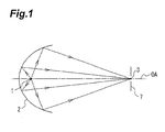
- Fig. 1 shows an example of a conventional collector optical system.
- a collective mirror 2 has a reflecting surface shaped in an ellipsoid of revolution, and, when the plasma light source 1 is positioned at the first focal point of the ellipsoid (hereinafter referred to as the first focal point), the EUV light reflected on the collective mirror 2 is collected at the second focal point of the ellipsoid (hereinafter referred to as the second focal point) to form a light source image 3 there.
- a stop 7 for blocking beams directly incident from the EUV light source 1 without being collected is located on a plane passing the second focal point of the collective mirror 2 and being perpendicular to the optical axis (hereinafter referred to as a second focal plane).
- An illumination optical system is located downstream of this stop 7.
- most of beams traveling from plasma light source 1 to the downstream area are not collected by the collective mirror 2 to be wasted.
- a conceivable means for collecting such beams traveling to the downstream area as well is the collector optical system as shown in Fig. 2 .
- Part of the EUV light diverging isotropically is also collected by collective mirror 2 having a reflecting surface shaped in an ellipsoid of revolution similar to the conventional collective mirror shown in Fig. 1 , to form a light source image 3 on the second focal plane.
- collective mirror 2 having a reflecting surface shaped in an ellipsoid of revolution similar to the conventional collective mirror shown in Fig. 1 , to form a light source image 3 on the second focal plane.
- other part of the EUV light is reflected by an auxiliary collective mirror 4 having a reflecting surface of spherical shape centered on the position of plasma light source 1, to be once collected at the same position as the plasma light source 1 is located. Thereafter, the light is reflected by the collective mirror 2 to be focused at the same position as the light source image 3 is formed.
- a real image of the plasma light source 1 by the collective mirror 2 and a real image by an optical system as a combination of auxiliary collective mirror 4 with collective mirror 2 are formed as superimposed at the position of light source image 3.
- collector optical system Since this collector optical system is able to guide the beams diverging from the plasma light source 1, over a wider range of solid angles to the light source image 3, the quantity of light guided to the illumination optical system increases.
- the collector optical systems based on this idea are already put in practical use as collector optical systems of projectors or the like (e.g., production information of Panasonic DLP projector Lightia TH-D9610J [browsed May 26, 2003], Internet ⁇ http://panasonic.bizlprojector/lightia/d9610/kido.html>).
- the plasma used as an EUV light source strongly absorbs the EUV light in general.
- the reason why the EUV light of a specific wavelength is generated from the plasma is that an electron transits between energy levels inherent to an atom. Light is generated upon a transition to a lower energy level, whereas light of the same wavelength is absorbed upon a transition to a higher energy level. Therefore, light generated from a plasma is essentially largely absorbed by the plasma.
- the present invention has been accomplished in light of the above problem and an object of the invention is to construct a collector optical system so that the plasma does not absorb the EUV light reflected by the auxiliary collective mirror, thereby increasing the sum of collected EUV light, and to apply this collector optical system to an EUV exposure apparatus, thereby achieving a large increase of throughput.
- the present invention adopts the following means.
- a collector optical system is a light source unit of EUV light comprising: a plasma light source for emitting EUV light; a collective mirror which has a reflecting surface of an ellipsoid of revolution and at a first focal point (a focal point of the ellipsoid) of which the plasma light source is located; and an auxiliary collective mirror which has a reflecting surface of a spherical surface and a center of the spherical surface of which is located as displaced from a position of the plasma light source.
- this configuration can prevent the plasma from absorbing the EUV light reflected by the auxiliary collective mirror.
- the center of the spherical surface of the auxiliary collective mirror is positioned in a plane passing the first focal point of the collective mirror and being perpendicular to the optical axis (agreeing with an axis of the ellipsoid) (the plane will be referred to as a first focal plane of the ellipsoidal mirror) and is displaced by a distance equal to or larger than a radius of the plasma light source from the optical axis.
- the center of the spherical surface of the auxiliary collective mirror is displaced by the distance equal to or larger than the radius of the plasma light source, the image of the plasma light source by the auxiliary collective mirror is positioned as displaced by the distance equal to or larger than the radius and is not formed at the position of the plasma light source. Therefore, It can more securely prevent the plasma from absorbing the EUV light reflected by the auxiliary collective mirror.
- the auxiliary collective mirror is comprised of a plurality of mirror elements having respective positions of spherical centers different from each other.
- the auxiliary collective mirror is comprised of the plurality of mirror elements having the respective positions of spherical centers different from each other and this configuration increases the number of light source images formed on an entrance plane of an optical integrator described hereinafter, which improves illuminance uniformity on a mask surface after passage through an illumination optical system.
- collector optical system is a collector optical system comprising a collective mirror having a reflecting surface of an ellipsoid of revolution; and an auxiliary collective mirror comprised of a spherical surface having a spherical center at a first focal point of the collective mirror, which satisfies R > (t ⁇ c)/2, where R is a radius of the auxiliary collective mirror, t a duration of pulsed light from a plasma light source, and c the speed of light.
- a round-trip distance between the plasma light source and the auxiliary collective mirror becomes longer than a distance (t ⁇ c) which is a product of the duration (t) of the pulsed light from the plasma light source and the speed of light (c). Therefore, when the EUV light reflected by the auxiliary collective mirror 2 comes back to the position of the plasma light source, the plasma is already extinct, so that the EUV light is not absorbed by the plasma.
- the plasma light source for emitting the EUV light it is also preferable to place the plasma light source for emitting the EUV light, at the first focal point of the collector optical system.
- the round-trip distance between the light source and the auxiliary collective mirror is longer than the distance (t ⁇ c) being the product of the duration (t) of pulsed light from the plasma light source and the speed of light (c). Therefore, when the EUV light reflected by the auxiliary collective mirror 2 comes back to the position of the plasma light source, the plasma is already extinct, so that the EUV light is not absorbed by the plasma.
- the EUV light can be collected while well suppressing loss of light quantity.
- the collective mirror is divided into a partial mirror located near and a partial mirror located away from the plasma light source and only the partial mirror located near the plasma light source is arranged to be replaceable.
- the reflecting surface is affected by radiant heat from the plasma light source and by heat from irradiation of the EUV light, and thus only the partial mirror heavily damaged thereby can be removed and readily replaced.
- An illumination optical apparatus comprises the light source unit as described above, and an illumination optical system for guiding the EUV light from the light source unit to a mask.
- the illumination optical apparatus is able to supply the EUV light from the light source unit without substantial loss of light quantity and to illuminate the mask with a predetermined pattern formed thereon, under a good illumination condition through the use of an optical integrator.
- An exposure apparatus is an exposure apparatus comprising an illumination optical apparatus for illuminating a reflective mask on which a predetermined pattern is formed; a mask stage for holding the mask placed on a surface to be illuminated by the illumination optical apparatus; a wafer stage for holding a wafer; a projection optical system for projecting the predetermined pattern formed on the mask, at a predetermined demagnification ratio onto the wafer; and a driving unit for relatively moving the mask stage and the wafer stage relative to the projection optical system at a speed according to the demagnification ratio in synchronism on the occasion of projecting the predetermined pattern formed on the mask, onto the wafer, wherein the illumination optical apparatus is the one as defined above.
- the position of the spherical center of the auxiliary collective mirror is a little displaced from the position of the plasma light source, whereby the EUV light reflected by the auxiliary collective mirror is not absorbed by the plasma.
- This enables much more EUV light than before to be efficiently collected.
- the round-trip distance between the plasma light source and the auxiliary collective mirror is set longer than the distance being the product of the duration of pulsed light from the plasma light source and the speed of light, whereby the plasma becomes extinct before the EUV light from the plasma light source comes back after reflected by the auxiliary collective mirror. Therefore, the EUV light reflected by the auxiliary collective mirror is not absorbed by the plasma. This enables much more EUV light than before to be efficiently collected.
- the light source unit with drastically increased efficiency of collection of light is applied to the exposure apparatus, it becomes feasible to achieve a significant increase of throughput.
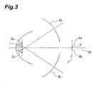
- Fig. 3 shows a light source unit being an embodiment of the present invention.
- a plasma light source 1 is located at the first focal point of collective mirror 2 having a reflecting surface shaped in an ellipsoid of revolution (i.e., at a focal point of the ellipsoid).
- Auxiliary collective mirror elements 4a, 4b are arranged as inclined so that respective spherical centers Ca, Cb thereof are displaced by ⁇ 0.25 mm, respectively, in the direction perpendicular to the optical axis OA from the position of the plasma light source 1.
- Part of the EUV light emitted from the plasma light source 1 is reflected by the collective mirror 2 to form a light source image 3 on the second focal plane of the ellipsoid.
- the size (diameter) of the plasma light source 1 is about 500 ⁇ m, and therefore the light source images 5a, 5b do not overlap with the plasma position, so as to be able to avoid absorption by the plasma.
- the light source images 5a, 5b are reflected by the collective mirror 2 to form light source images 6a, 6b on the second focal plane of the ellipsoid.
- a stop 7 for removing stray light is located on the second focal plane of the ellipsoid, and the light source images 3, 6a, 6b are formed as juxtaposed on an aperture provided in this stop 7.
- An illumination optical system (described later) is provided downstream the stop 7 and beams diverging from the light source images 3, 6a, 6b are guided thereto.
- the stop 7 can also serve as a vacuum bulkhead for differential pumping between the light source unit and the part where the illumination optical system and others are located.
- the illumination optical system in the exposure apparatus is constructed using an optical integrator for dividing a beam diverging from a light source to form a plurality of light source images, for implementing Köhler illumination.
- the use of the optical integrator can uniform an intensity distribution of illumination light projected onto a mask.
- the collector optical system of the light source unit according to the present invention is arranged to form a plurality of light source images 3, 6a, 6b, it can be used as a part of functionality of the optical integrator.
- Fig. 3 provides a side view, and, when the collector optical system is viewed from the direction of the optical axis OA, the auxiliary collective mirror is divided into four elements 4a-4d in fact, as shown in Fig. 4(a) , and thus five light source images 3, 6a-6d are formed on the focal plane, as shown in Fig. 4(b) . Since the number of light source images formed on the entrance plane of the optical integrator is increased, the illuminance uniformity is improved on the exit plane of the optical integrator.
- the auxiliary collective mirror may be divided into eight elements 4a-4h, as shown in Fig. 5(a) .
- nine light source images 3, 6a-6h are formed on the focal plane, as shown in Fig. 5(b) . It is noted that how to divide the auxiliary collective mirror is not limited to the above examples.
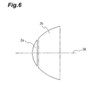
- Fig. 6 is a side view of a modification example of collective mirror 2 shown in Fig. 1 .
- the collective mirror can also be divided into two elements, a partial mirror 2a located near the plasma and a partial mirror 2b located away from the plasma.
- the reflecting surface is affected by radiant heat from the plasma light source 1 and by heat from irradiation of EUV light and it is thus anticipated that there arises a need for removing and replacing only the partial mirror 2a heavily damaged. Therefore, it is desirable to adopt such a readily replaceable configuration.
- Fig. 7 shows a light source unit being an embodiment of the present invention.
- the plasma light source 1 is arranged to collect light emitted from a laser light source LS (non-EUV light), through a lens 12 and a through-hole of collective mirror 2.
- the plasma light source 1 is located at the first focal point of collective mirror 2 having a reflecting surface shaped in an ellipsoid of revolution.
- the EUV light emitted from the plasma light source 1 is reflected by the auxiliary collective mirror 4 to form a light source image 3 at the same position as the plasma light source 1 is located.
- the distance from the plasma light source 1 to the auxiliary collective mirror 2 is 40 cm.
- the plasma light source used herein is a laser produced plasma light source (LPP) and the duration of pulsed light from the plasma light source is 2 ns.
- LPP laser produced plasma light source
- the EUV light emitted from the plasma light source 1 travels through the distance of 80 cm before it comes back to the position of the plasma light source 1 after reflected by the auxiliary collective mirror 2, and it thus takes the time of 2.7 ns.
- the plasma Since the duration of pulsed light from the plasma light source is 2 ns, the plasma is already extinct when even the light generated in the initial part of a pulse comes back to the position of the plasma light source 1 after reflected by the auxiliary collective mirror 2. Therefore, the EUV light is not absorbed by the plasma. Beams traveling from this light source image are reflected by the collective mirror 2 to form a light source image 3 on the second focal plane of the ellipsoid. Namely, a real image of the plasma light source 1 by the collective mirror 2 and a real image by the optical system as a combination of the auxiliary collective mirror 4 with the collective mirror 2 are formed at the same position of the light source image 3 but at different times.
- a stop 7 for removing stray light is provided on the focal plane of the ellipsoid and the light source image 3 is formed on an aperture provided in this stop 7.
- An illumination optical system (not shown) is provided downstream the stop and beams diverging from the light source image 3 are guided thereto.
- the stop 7 can also serve as a vacuum bulkhead for differential pumping between the light source part and the part where the illumination optical system and others are located.
- Fig. 8 shows an embodiment of an EUV exposure apparatus incorporating an illumination optical system using the light source unit being the first embodiment of the present invention, and a rod type optical integrator proposed by Applicant of the present application et al. (Japanese Patent Application No. 2000-068114 ).
- Fig. 8 is an illustration showing a schematic configuration of a first projection exposure apparatus according to the present embodiment, and the projection exposure apparatus is roughly composed of a light source unit LU, an illumination optical system IU, and a projection optical system PL. These are located in a vacuum state in a chamber, or in a chamber filled with a gas (e.g., helium) demonstrating little absorption to at least a wavelength to be used.
- a gas e.g., helium
- the plasma light source 1 is arranged so that light emitted from a laser light source LS (non-EUV light) is collected through a lens 12 and a through-hole of collective mirror 2 onto a gas target 13.
- a laser light source LS non-EUV light
- the laser light source LS is desirably arranged as a little inclined relative to the optical axis OA so as to prevent the laser light (non-EUV light) from directly entering the illumination optical system IU downstream the second focal point CP of the collective mirror 2.
- the gas target 13 is formed from a gas ejected from a gas nozzle 14, e.g., a high-pressure gas of xenon (Xe).
- the gas target 13 turns into a plasma by energy from the collected laser light to emit EUV light.
- the gas target 13 is positioned at the first focal point of collective mirror 2. Therefore, the EUV light emitted from the plasma light source 1 is collected at the second focal point CP of the collective mirror 2.
- the auxiliary collective mirror 4 is comprised of two mirror elements and the two mirror elements are arranged as inclined so that their respective spherical centers are displaced by ⁇ 0.25 mm, respectively, in the direction perpendicular to the optical axis OA from the position of the plasma light source 1.
- the illumination optical system IU is composed of an optical integrator 10 and an imaging system composed of a concave mirror M2 and a convex mirror M3.
- the optical integrator 10 is arranged so that its entrance end face 10F is located near the second focal point CP of the collective mirror 2, and light reflected on the internal wall surface of the optical integrator 10 and passing therethrough is emitted from an exit end face 10B.
- the light emerging from the exit end face 10B of the optical integrator 10 is reflected by the concave mirror M2, reflected by the convex mirror M3, and further reflected by the concave mirror M2 to illuminate a reflective mask R.
- a device pattern surface of the mask R is arranged in the conjugate relation with the exit end face 10B of the optical integrator 10. As described with Fig. 2 , the exit end face 10B is illuminated with good uniformity in plane, and thus the surface of the mask R is also uniformly illuminated.
- the projection optical system PL is comprised of a concave mirror M4, a convex mirror M5, a concave mirror M6, and a concave mirror M7 arranged in the order named from the mask R side.
- the concave mirror M4, concave mirror M6, and concave mirror M7 are formed in an aspherical shape. This configuration is disclosed, for example, in Japanese Patent Application Laid-Open No. 9-251097 .
- the light reflected by the reflective mask R travels via the projection optical system PL to form a device pattern on a wafer W coated with a resist. Since an illuminated area on the mask R is smaller than the area of the device pattern of the mask, the mask R and the wafer W are scanned in synchronism, as indicated by arrows in Fig. 6 , to effect exposure of the entire device pattern. After completion of the exposure of the entire device pattern, the wafer is stepped to a next exposure area. By repeating this operation, i.e., by the step-and-scan method, a plurality of device patterns are formed on the entire wafer.
- the present embodiment described the example using the rod type optical integrator, but it is also possible to use a reflection type optical integrator, as described in Japanese Patent Application Laid-Open No. ( JP-A) 11-312638 .
- JP-A Japanese Patent Application Laid-Open No.
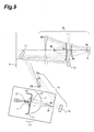
- An example of an EUV exposure apparatus using a reflective optical integrator will be described with reference to Fig. 9 .
- the light source unit in the present embodiment has the same configuration as the light source unit of Embodiment 3 shown in Fig. 8 , and thus description of redundant part is omitted herein.
- the EUV light collected at the second focal point CP of the collective mirror 2 is guided via a collimator mirror 15 to an integrator 16 consisting of a pair of fly's eye mirrors 16a and 16b.
- An example of the pair of fly's eye mirrors 16a and 16b is the fly's eye mirrors disclosed, for example, in JP-A 11-312638 by Applicant of the present application. Concerning the further detailed configuration and action of the fly's eye mirrors, reference can be made, for example, to the related description in JP-A 11-312638 .
- a substantial surface illuminant having a predetermined shape is formed near the reflecting surface of the second fly's eye mirror 16b, i.e., near the exit plane of optical integrator 16.
- Light from the substantial surface illuminant is deflected by a plane mirror 17 and thereafter travels via a field stop (not shown) to form an illumination area of an arcuate shape elongated on the mask R.
- Light from the pattern on the mask R thus illuminated travels via the projection optical system PL to form an image of the mask pattern on the wafer W.
- the projection optical system PL is composed of six mirrors arranged in order from the mask R side. For example, this configuration is disclosed in JP-A 11-312638 .
- the plasma light source 1 as a collector optical system is arranged at the first focal point of the collective mirror 2 having the reflecting surface of the shape of the ellipsoid of revolution (i.e., at the focal point of the ellipsoid) and the auxiliary collective mirror elements 4a, 4b are arranged as inclined so that their respective spherical centers are displaced by ⁇ 0.25 mm, respectively, in the direction perpendicular to the optical axis OA from the position of the plasma light source 1.
- the collector optical system can be a collector optical system comprising a collective mirror having a reflecting surface of an ellipsoid of revolution, and an auxiliary collective mirror consisting of a spherical surface with its spherical center at the first focal point of the collective mirror, which is arranged to satisfy R > (t ⁇ c)/2, where R is a radius of the auxiliary collective mirror, t a duration of pulsed light from the plasma light source, and c the speed of light.
- the foregoing embodiment uses the light source of the LPP type as a plasma light source, but, without having to be limited to this, it is also possible to use a light source of the DPP type.
- the position of the spherical center of the auxiliary collective mirror is a little displaced from the position of the plasma light source, whereby the EUV light reflected by the auxiliary collective mirror is not absorbed by the plasma.
- This enables much more EUV light than before to be efficiently collected.
- the round-trip distance between the plasma light source and the auxiliary collective mirror is set longer than the distance being the product of the duration of the pulsed light from the plasma light source and the speed of light, whereby the plasma becomes extinct before the EUV light from the plasma light source comes back after reflected by the auxiliary collective mirror. Therefore, the EUV light reflected by the auxiliary collective mirror is not absorbed by the plasma. This enables much more EUV light than before to be efficiently collected.
- the light source unit with drastically increased efficiency of collection of light is applied to the exposure apparatus, it becomes feasible to achieve a significant increase of throughput.
Abstract
Description
- The present invention relates to a collector optical system, illumination optical apparatus, and exposure apparatus. More particularly, the present invention relates to a collector optical system suitably applicable to the exposure apparatus used in production of microdevices such as semiconductor elements by photolithography, using EUV light (Extreme Ultra Violet light) having the wavelength of approximately 5-50 nm.
- The exposure apparatus for production of semiconductor devices is arranged to project and transcribe a circuit pattern formed on a mask, onto a photosensitive substrate such as a wafer coated with a resist, through a projection optical system.
- With the exposure apparatus of this type, there are desires for a further improvement in resolving power as the circuit pattern to be transcribed becomes finer and finer, and light of a shorter wavelength is being used as exposure light. In recent years, the exposure apparatus using the EUV (Extreme Ultra Violet) light with the wavelength of approximately 5 to 50 nm (hereinafter referred to as "EUVL (Extreme UltraViolet Lithography) exposure apparatus") has been proposed as next-generation equipment.
- At present, there are the following three types of light sources proposed heretofore, as light sources for supplying the EUV light:
- (1) Light sources for supplying SR (synchrotron radiation);
- (2) LPP (Laser Produced Plasma) light sources for obtaining the EUV light by focusing a laser beam on a target to turn the target into a plasma;
- (3) DPP (Discharge Produced Plasma) light sources for obtaining the EUV light by applying a voltage on an electrode of a target substance, or between electrodes in a state in which a target substance is present between the electrodes, to turn the target material into a plasma.
- The DPP light sources and LPP light sources will be generically referred to hereinafter as "plasma light sources."
- The EUV light is isotropically radiated from a plasma light source. Namely, the plasma light source can be regarded as a point light source. The size (diameter) of the plasma light source is approximately from 50 to 500 µm.
-
Fig. 1 shows an example of a conventional collector optical system. Acollective mirror 2 has a reflecting surface shaped in an ellipsoid of revolution, and, when the plasma light source 1 is positioned at the first focal point of the ellipsoid (hereinafter referred to as the first focal point), the EUV light reflected on thecollective mirror 2 is collected at the second focal point of the ellipsoid (hereinafter referred to as the second focal point) to form alight source image 3 there. Astop 7 for blocking beams directly incident from the EUV light source 1 without being collected is located on a plane passing the second focal point of thecollective mirror 2 and being perpendicular to the optical axis (hereinafter referred to as a second focal plane). An illumination optical system is located downstream of thisstop 7.
In the above-described collector optical system as shown inFig. 1 , most of beams traveling from plasma light source 1 to the downstream area (to the right inFig. 1 ) are not collected by thecollective mirror 2 to be wasted. A conceivable means for collecting such beams traveling to the downstream area as well is the collector optical system as shown inFig. 2 . - Part of the EUV light diverging isotropically is also collected by
collective mirror 2 having a reflecting surface shaped in an ellipsoid of revolution similar to the conventional collective mirror shown inFig. 1 , to form alight source image 3 on the second focal plane. On the other hand, other part of the EUV light is reflected by an auxiliarycollective mirror 4 having a reflecting surface of spherical shape centered on the position of plasma light source 1, to be once collected at the same position as the plasma light source 1 is located. Thereafter, the light is reflected by thecollective mirror 2 to be focused at the same position as thelight source image 3 is formed. - Namely, a real image of the plasma light source 1 by the
collective mirror 2 and a real image by an optical system as a combination of auxiliarycollective mirror 4 withcollective mirror 2 are formed as superimposed at the position oflight source image 3. - Since this collector optical system is able to guide the beams diverging from the plasma light source 1, over a wider range of solid angles to the
light source image 3, the quantity of light guided to the illumination optical system increases. The collector optical systems based on this idea are already put in practical use as collector optical systems of projectors or the like (e.g., production information of Panasonic DLP projector Lightia TH-D9610J [browsed May 26, 2003], Internet <http://panasonic.bizlprojector/lightia/d9610/kido.html>). - The plasma used as an EUV light source strongly absorbs the EUV light in general. The reason why the EUV light of a specific wavelength is generated from the plasma is that an electron transits between energy levels inherent to an atom. Light is generated upon a transition to a lower energy level, whereas light of the same wavelength is absorbed upon a transition to a higher energy level. Therefore, light generated from a plasma is essentially largely absorbed by the plasma.
- Therefore, the collector optical system of
Fig. 2 cannot be applied directly to the EUV exposure apparatus. - The reason is that in the collector optical system of
Fig. 2 the EUV light reflected by auxiliarycollective mirror 4 and returning to the position of EUV light source 1 is absorbed by the plasma and thus cannot reach the position of thelight source image 3 in fact. Accordingly, there is no increase in the total quantity of the collected EUV light. - The present invention has been accomplished in light of the above problem and an object of the invention is to construct a collector optical system so that the plasma does not absorb the EUV light reflected by the auxiliary collective mirror, thereby increasing the sum of collected EUV light, and to apply this collector optical system to an EUV exposure apparatus, thereby achieving a large increase of throughput.
- In order to solve the above problem, the present invention adopts the following means.
- A collector optical system according to the present invention is a light source unit of EUV light comprising: a plasma light source for emitting EUV light; a collective mirror which has a reflecting surface of an ellipsoid of revolution and at a first focal point (a focal point of the ellipsoid) of which the plasma light source is located; and an auxiliary collective mirror which has a reflecting surface of a spherical surface and a center of the spherical surface of which is located as displaced from a position of the plasma light source.
- Since in the light source unit the center of the spherical surface of the auxiliary collective mirror is displaced from the position of the plasma light source, an image of the plasma light source by the auxiliary collective mirror is not formed at the position of the plasma light source. Therefore, this configuration can prevent the plasma from absorbing the EUV light reflected by the auxiliary collective mirror.
- Furthermore, in the above collector optical system, preferably, the center of the spherical surface of the auxiliary collective mirror is positioned in a plane passing the first focal point of the collective mirror and being perpendicular to the optical axis (agreeing with an axis of the ellipsoid) (the plane will be referred to as a first focal plane of the ellipsoidal mirror) and is displaced by a distance equal to or larger than a radius of the plasma light source from the optical axis.
- Since in the above collector optical system the center of the spherical surface of the auxiliary collective mirror is displaced by the distance equal to or larger than the radius of the plasma light source, the image of the plasma light source by the auxiliary collective mirror is positioned as displaced by the distance equal to or larger than the radius and is not formed at the position of the plasma light source. Therefore, It can more securely prevent the plasma from absorbing the EUV light reflected by the auxiliary collective mirror.
- In the light source unit, preferably, the auxiliary collective mirror is comprised of a plurality of mirror elements having respective positions of spherical centers different from each other.
- In the above light source unit, the auxiliary collective mirror is comprised of the plurality of mirror elements having the respective positions of spherical centers different from each other and this configuration increases the number of light source images formed on an entrance plane of an optical integrator described hereinafter, which improves illuminance uniformity on a mask surface after passage through an illumination optical system.
- Another preferred configuration of the collector optical system is a collector optical system comprising a collective mirror having a reflecting surface of an ellipsoid of revolution; and an auxiliary collective mirror comprised of a spherical surface having a spherical center at a first focal point of the collective mirror, which satisfies R > (t×c)/2, where R is a radius of the auxiliary collective mirror, t a duration of pulsed light from a plasma light source, and c the speed of light.
- In the collector optical system, when the plasma light source is placed at the position of the first focal point, a round-trip distance between the plasma light source and the auxiliary collective mirror becomes longer than a distance (t×c) which is a product of the duration (t) of the pulsed light from the plasma light source and the speed of light (c). Therefore, when the EUV light reflected by the auxiliary
collective mirror 2 comes back to the position of the plasma light source, the plasma is already extinct, so that the EUV light is not absorbed by the plasma. - In the foregoing light source unit, it is also preferable to place the plasma light source for emitting the EUV light, at the first focal point of the collector optical system.
In the above light source mit, the round-trip distance between the light source and the auxiliary collective mirror is longer than the distance (t×c) being the product of the duration (t) of pulsed light from the plasma light source and the speed of light (c). Therefore, when the EUV light reflected by the auxiliarycollective mirror 2 comes back to the position of the plasma light source, the plasma is already extinct, so that the EUV light is not absorbed by the plasma. In addition, the EUV light can be collected while well suppressing loss of light quantity. - In the above light source unit, preferably, the collective mirror is divided into a partial mirror located near and a partial mirror located away from the plasma light source and only the partial mirror located near the plasma light source is arranged to be replaceable.
- In the above light source unit, the reflecting surface is affected by radiant heat from the plasma light source and by heat from irradiation of the EUV light, and thus only the partial mirror heavily damaged thereby can be removed and readily replaced.
- An illumination optical apparatus according to the present invention comprises the light source unit as described above, and an illumination optical system for guiding the EUV light from the light source unit to a mask.
The illumination optical apparatus is able to supply the EUV light from the light source unit without substantial loss of light quantity and to illuminate the mask with a predetermined pattern formed thereon, under a good illumination condition through the use of an optical integrator. - An exposure apparatus according to the present invention is an exposure apparatus comprising an illumination optical apparatus for illuminating a reflective mask on which a predetermined pattern is formed; a mask stage for holding the mask placed on a surface to be illuminated by the illumination optical apparatus; a wafer stage for holding a wafer; a projection optical system for projecting the predetermined pattern formed on the mask, at a predetermined demagnification ratio onto the wafer; and a driving unit for relatively moving the mask stage and the wafer stage relative to the projection optical system at a speed according to the demagnification ratio in synchronism on the occasion of projecting the predetermined pattern formed on the mask, onto the wafer, wherein the illumination optical apparatus is the one as defined above.
- According to the present invention, as described above, the position of the spherical center of the auxiliary collective mirror is a little displaced from the position of the plasma light source, whereby the EUV light reflected by the auxiliary collective mirror is not absorbed by the plasma. This enables much more EUV light than before to be efficiently collected. By applying the light source unit with drastically increased efficiency of collection of light as described above, to the exposure apparatus, it becomes feasible to achieve a significant increase of throughput.
- In the present invention, the round-trip distance between the plasma light source and the auxiliary collective mirror is set longer than the distance being the product of the duration of pulsed light from the plasma light source and the speed of light, whereby the plasma becomes extinct before the EUV light from the plasma light source comes back after reflected by the auxiliary collective mirror. Therefore, the EUV light reflected by the auxiliary collective mirror is not absorbed by the plasma. This enables much more EUV light than before to be efficiently collected. When the light source unit with drastically increased efficiency of collection of light is applied to the exposure apparatus, it becomes feasible to achieve a significant increase of throughput.
-
-
Fig. 1 is an illustration showing a conventional collector optical system. -
Fig. 2 is an illustration showing a collector optical system using a conventional auxiliary collective mirror. -
Fig. 3 is an illustration showing a collector optical system being an embodiment of the present invention. -
Fig. 4 is an illustration showing an example of an auxiliary collective mirror. -
Fig. 5 is an illustration showing an example of an auxiliary collective mirror. -
Fig. 6 is an illustration showing a modification example of a collective mirror according to the present invention. -
Fig. 7 is an illustration showing a collector optical system using an auxiliary collective mirror according to the present invention. -
Fig. 8 is an illustration showing an example of an EUV exposure apparatus using a collector optical system according to the present invention. -
Fig. 9 is an illustration showing an example of an EUV exposure apparatus using a collector optical system according to the present invention. - Embodiments of the present invention will be described on the basis of the accompanying drawings.
-
Fig. 3 shows a light source unit being an embodiment of the present invention. - A plasma light source 1 is located at the first focal point of
collective mirror 2 having a reflecting surface shaped in an ellipsoid of revolution (i.e., at a focal point of the ellipsoid). Auxiliarycollective mirror elements collective mirror 2 to form alight source image 3 on the second focal plane of the ellipsoid. - Other part of the EUV light emitted from the plasma light source 1 is reflected by the auxiliary
collective mirror elements light source images light source images
Thelight source images collective mirror 2 to formlight source images stop 7 for removing stray light is located on the second focal plane of the ellipsoid, and thelight source images stop 7. An illumination optical system (described later) is provided downstream thestop 7 and beams diverging from thelight source images stop 7 can also serve as a vacuum bulkhead for differential pumping between the light source unit and the part where the illumination optical system and others are located. - In general, the illumination optical system in the exposure apparatus is constructed using an optical integrator for dividing a beam diverging from a light source to form a plurality of light source images, for implementing Köhler illumination. The use of the optical integrator can uniform an intensity distribution of illumination light projected onto a mask.
- Since the collector optical system of the light source unit according to the present invention is arranged to form a plurality of
light source images -
Fig. 3 provides a side view, and, when the collector optical system is viewed from the direction of the optical axis OA, the auxiliary collective mirror is divided into fourelements 4a-4d in fact, as shown inFig. 4(a) , and thus fivelight source images Fig. 4(b) . Since the number of light source images formed on the entrance plane of the optical integrator is increased, the illuminance uniformity is improved on the exit plane of the optical integrator. - The auxiliary collective mirror may be divided into eight
elements 4a-4h, as shown inFig. 5(a) . In this case, ninelight source images Fig. 5(b) . It is noted that how to divide the auxiliary collective mirror is not limited to the above examples. -
Fig. 6 is a side view of a modification example ofcollective mirror 2 shown inFig. 1 . As shown inFig. 6 , the collective mirror can also be divided into two elements, apartial mirror 2a located near the plasma and apartial mirror 2b located away from the plasma. Particularly, the reflecting surface is affected by radiant heat from the plasma light source 1 and by heat from irradiation of EUV light and it is thus anticipated that there arises a need for removing and replacing only thepartial mirror 2a heavily damaged. Therefore, it is desirable to adopt such a readily replaceable configuration. -
Fig. 7 shows a light source unit being an embodiment of the present invention. Referring toFig. 7 , the plasma light source 1 is arranged to collect light emitted from a laser light source LS (non-EUV light), through alens 12 and a through-hole ofcollective mirror 2. The plasma light source 1 is located at the first focal point ofcollective mirror 2 having a reflecting surface shaped in an ellipsoid of revolution. There is an auxiliarycollective mirror 4 having a reflecting surface of a spherical shape centered on the position of the first focal point. Part of the EUV light emitted from the plasma light source 1 is reflected by thecollective mirror 2 to form alight source image 3 on the second focal plane of the ellipsoid. Other part of the EUV light emitted from the plasma light source 1 is reflected by the auxiliarycollective mirror 4 to form alight source image 3 at the same position as the plasma light source 1 is located. The distance from the plasma light source 1 to the auxiliarycollective mirror 2 is 40 cm. The plasma light source used herein is a laser produced plasma light source (LPP) and the duration of pulsed light from the plasma light source is 2 ns. The EUV light emitted from the plasma light source 1 travels through the distance of 80 cm before it comes back to the position of the plasma light source 1 after reflected by the auxiliarycollective mirror 2, and it thus takes the time of 2.7 ns. Since the duration of pulsed light from the plasma light source is 2 ns, the plasma is already extinct when even the light generated in the initial part of a pulse comes back to the position of the plasma light source 1 after reflected by the auxiliarycollective mirror 2. Therefore, the EUV light is not absorbed by the plasma. Beams traveling from this light source image are reflected by thecollective mirror 2 to form alight source image 3 on the second focal plane of the ellipsoid. Namely, a real image of the plasma light source 1 by thecollective mirror 2 and a real image by the optical system as a combination of the auxiliarycollective mirror 4 with thecollective mirror 2 are formed at the same position of thelight source image 3 but at different times. Astop 7 for removing stray light is provided on the focal plane of the ellipsoid and thelight source image 3 is formed on an aperture provided in thisstop 7. An illumination optical system (not shown) is provided downstream the stop and beams diverging from thelight source image 3 are guided thereto. Thestop 7 can also serve as a vacuum bulkhead for differential pumping between the light source part and the part where the illumination optical system and others are located. -
Fig. 8 shows an embodiment of an EUV exposure apparatus incorporating an illumination optical system using the light source unit being the first embodiment of the present invention, and a rod type optical integrator proposed by Applicant of the present application et al. (Japanese Patent Application No.2000-068114 -
Fig. 8 is an illustration showing a schematic configuration of a first projection exposure apparatus according to the present embodiment, and the projection exposure apparatus is roughly composed of a light source unit LU, an illumination optical system IU, and a projection optical system PL. These are located in a vacuum state in a chamber, or in a chamber filled with a gas (e.g., helium) demonstrating little absorption to at least a wavelength to be used. - With reference to
Fig. 8 , the plasma light source 1 is arranged so that light emitted from a laser light source LS (non-EUV light) is collected through alens 12 and a through-hole ofcollective mirror 2 onto agas target 13. - The laser light source LS is desirably arranged as a little inclined relative to the optical axis OA so as to prevent the laser light (non-EUV light) from directly entering the illumination optical system IU downstream the second focal point CP of the
collective mirror 2. Here thegas target 13 is formed from a gas ejected from agas nozzle 14, e.g., a high-pressure gas of xenon (Xe). Thegas target 13 turns into a plasma by energy from the collected laser light to emit EUV light. Thegas target 13 is positioned at the first focal point ofcollective mirror 2. Therefore, the EUV light emitted from the plasma light source 1 is collected at the second focal point CP of thecollective mirror 2. On the other hand, the gas after completion of light emission is drawn through acollector 11 to be guided to the outside. The auxiliarycollective mirror 4 is comprised of two mirror elements and the two mirror elements are arranged as inclined so that their respective spherical centers are displaced by ±0.25 mm, respectively, in the direction perpendicular to the optical axis OA from the position of the plasma light source 1. - The illumination optical system IU is composed of an
optical integrator 10 and an imaging system composed of a concave mirror M2 and a convex mirror M3. Theoptical integrator 10 is arranged so that its entrance end face 10F is located near the second focal point CP of thecollective mirror 2, and light reflected on the internal wall surface of theoptical integrator 10 and passing therethrough is emitted from an exit end face 10B. - The light emerging from the
exit end face 10B of theoptical integrator 10 is reflected by the concave mirror M2, reflected by the convex mirror M3, and further reflected by the concave mirror M2 to illuminate a reflective mask R. A device pattern surface of the mask R is arranged in the conjugate relation with theexit end face 10B of theoptical integrator 10. As described withFig. 2 , theexit end face 10B is illuminated with good uniformity in plane, and thus the surface of the mask R is also uniformly illuminated. - The projection optical system PL is comprised of a concave mirror M4, a convex mirror M5, a concave mirror M6, and a concave mirror M7 arranged in the order named from the mask R side. The concave mirror M4, concave mirror M6, and concave mirror M7 are formed in an aspherical shape. This configuration is disclosed, for example, in Japanese Patent Application Laid-Open No.
9-251097 - The light reflected by the reflective mask R travels via the projection optical system PL to form a device pattern on a wafer W coated with a resist. Since an illuminated area on the mask R is smaller than the area of the device pattern of the mask, the mask R and the wafer W are scanned in synchronism, as indicated by arrows in
Fig. 6 , to effect exposure of the entire device pattern. After completion of the exposure of the entire device pattern, the wafer is stepped to a next exposure area. By repeating this operation, i.e., by the step-and-scan method, a plurality of device patterns are formed on the entire wafer. - The present embodiment described the example using the rod type optical integrator, but it is also possible to use a reflection type optical integrator, as described in Japanese Patent Application Laid-Open No. (
JP-A) 11-312638 Fig. 9 . - The light source unit in the present embodiment has the same configuration as the light source unit of
Embodiment 3 shown inFig. 8 , and thus description of redundant part is omitted herein. The EUV light collected at the second focal point CP of thecollective mirror 2 is guided via acollimator mirror 15 to an integrator 16 consisting of a pair of fly's eye mirrors 16a and 16b. An example of the pair of fly's eye mirrors 16a and 16b is the fly's eye mirrors disclosed, for example, inJP-A 11-312638 JP-A 11-312638 - In this manner, a substantial surface illuminant having a predetermined shape is formed near the reflecting surface of the second fly's
eye mirror 16b, i.e., near the exit plane of optical integrator 16. Light from the substantial surface illuminant is deflected by aplane mirror 17 and thereafter travels via a field stop (not shown) to form an illumination area of an arcuate shape elongated on the mask R. Light from the pattern on the mask R thus illuminated travels via the projection optical system PL to form an image of the mask pattern on the wafer W. - The projection optical system PL is composed of six mirrors arranged in order from the mask R side. For example, this configuration is disclosed in
JP-A 11-312638 - In the above-described embodiment, the plasma light source 1 as a collector optical system is arranged at the first focal point of the
collective mirror 2 having the reflecting surface of the shape of the ellipsoid of revolution (i.e., at the focal point of the ellipsoid) and the auxiliarycollective mirror elements
Without having to be limited to this, however, the collector optical system can be a collector optical system comprising a collective mirror having a reflecting surface of an ellipsoid of revolution, and an auxiliary collective mirror consisting of a spherical surface with its spherical center at the first focal point of the collective mirror, which is arranged to satisfy R > (t×c)/2, where R is a radius of the auxiliary collective mirror, t a duration of pulsed light from the plasma light source, and c the speed of light. - The foregoing embodiment uses the light source of the LPP type as a plasma light source, but, without having to be limited to this, it is also possible to use a light source of the DPP type.
- According to the present invention, as described above, the position of the spherical center of the auxiliary collective mirror is a little displaced from the position of the plasma light source, whereby the EUV light reflected by the auxiliary collective mirror is not absorbed by the plasma. This enables much more EUV light than before to be efficiently collected. When the light source unit with drastically increased efficiency of collection of light as described above is applied to the exposure apparatus, it becomes feasible to achieve a significant increase of throughput.
- In the present invention, the round-trip distance between the plasma light source and the auxiliary collective mirror is set longer than the distance being the product of the duration of the pulsed light from the plasma light source and the speed of light, whereby the plasma becomes extinct before the EUV light from the plasma light source comes back after reflected by the auxiliary collective mirror. Therefore, the EUV light reflected by the auxiliary collective mirror is not absorbed by the plasma. This enables much more EUV light than before to be efficiently collected. When the light source unit with drastically increased efficiency of collection of light is applied to the exposure apparatus, it becomes feasible to achieve a significant increase of throughput.
- Example 1 describes a light source unit of EUV light comprising: a plasma light source for emitting EUV light; a collective mirror which has a reflecting surface of an ellipsoid of revolution and at a first focal point of which the plasma light source is located; and an auxiliary collective mirror which has a reflecting surface of a spherical surface and a center of the spherical surface of which is located as displaced from a position of the plasma light source.
- Example 2 describes the light source according to example 1 wherein the center of the spherical surface of the auxiliary collective mirror is located in a plane passing the first focal point of the collective mirror and being perpendicular to the optical axis, and is displaced by a distance equal to or larger than a radius of the plasma light source from the optical axis.
- Example 3 describes the light source unit according to example 1 or example 2, wherein the auxiliary collective mirror is comprised of a plurality of mirror elements having respective positions of spherical centers different from each other.
- Example 4 describes the light source unit according to example 3, wherein the auxiliary collective mirror is comprised of at least four mirror elements.
- Example 5 describes a collector optical system comprising a collective mirror having a reflecting surface of an ellipsoid of revolution, and an auxiliary collective mirror consisting of a spherical surface having a spherical center at a first focal point of the collective mirror; and arranged to collect pulsed light emitted from a plasma light source, the collector optical system satisfying R>(txc)/2, where R is a radius of the auxiliary collective mirror, t a duration of the pulsed light from the plasma light source, and c the speed of light.
- Example 6 describes the collector optical system according to example 5, wherein the radius of the auxiliary collective mirror is set to not less than 30 cm.
- Example 7 describes a light source unit wherein the plasma light source for emitting EUV light is placed at the first focal point of the collective mirror as defined in example 5 or example 6.
- Example 8 describes the light source unit according to any one of examples 1 to 4 or example 7, wherein the collective mirror is divided into a partial mirror located near and a partial mirror located away from the plasma light source, and wherein only the partial mirror located near the plasma light source is arranged so as to be replaceable.
- Example 9 describes an illumination optical apparatus comprising the light source unit as defined in any one of examples 1 to 4 or examples 7 and 8, and an illumination optical system for guiding the EUV light from the light source unit to a mask.
- Example 10 describes an exposure apparatus comprising: an illumination optical apparatus for illuminating a reflective mask on which a predetermined pattern is formed; a mask stage for holding a mask on a surface to be illuminated by the illumination optical apparatus; a wafer stage for holding a wafer; a projection optical system for projecting the predetermined pattern formed on the mask, at a predetermined demagnification ratio onto the wafer; and a driving unit for relatively moving the mask stage and the wafer stage relative to the projection optical system at a speed according to the demagnification ratio in synchronism on the occasion of projecting the predetermined pattern formed on the mask, onto the wafer, wherein the illumination optical apparatus is the illumination optical apparatus as defined in example 9.
Claims (6)
- A collector optical system comprising a collective mirror having a reflecting surface of an ellipsoid of revolution, and an auxiliary collective mirror consisting of a spherical surface having a spherical center at a first focal point of the collective mirror; and arranged to collect pulsed light emitted from a plasma light source,
the collector optical system satisfying R>(t×c)/2,
where R is a radius of the auxiliary collective mirror, t a duration of the pulsed light from the plasma light source, and c the speed of light. - The collector optical system according to claim 1, wherein the radius of the auxiliary collective mirror is set to not less than 30 cm.
- A light source unit wherein the plasma light source for emitting EUV light is placed at the first focal point of the collective mirror as defined in claim 1 or claim 2.
- The light source unit according to claim 3, wherein the collective mirror is divided into a partial mirror located near and a partial mirror located away from the plasma light source, and wherein only the partial mirror located near the plasma light source is arranged so as to be replaceable.
- An illumination optical apparatus comprising the light source unit as defined in any one of claim 3 or claim 4, and an illumination optical system for guiding the EUV light from the light source unit to a mask.
- An exposure apparatus comprising:an illumination optical apparatus for illuminating a reflective mask on which a predetermined pattern is formed;a mask stage for holding a mask on a surface to be illuminated by the illumination optical apparatus;a wafer stage for holding a wafer;a projection optical system for projecting the predetermined pattern formed on the mask, at a predetermined demagnification ratio onto the wafer; anda driving unit for relatively moving the mask stage and the wafer stage relative to the projection optical system at a speed according to the demagnification ratio in synchronism on the occasion of projecting the predetermined pattern formed on the mask, onto the wafer,wherein the illumination optical apparatus is the illumination optical apparatus as defined in claim 5.
Applications Claiming Priority (2)
| Application Number | Priority Date | Filing Date | Title |
|---|---|---|---|
| JP2003196194A JP4120502B2 (en) | 2003-07-14 | 2003-07-14 | Condensing optical system, light source unit, illumination optical apparatus, and exposure apparatus |
| EP04747519A EP1650786B1 (en) | 2003-07-14 | 2004-07-14 | Light source unit, illumination optical apparatus and exposure apparatus |
Related Parent Applications (2)
| Application Number | Title | Priority Date | Filing Date |
|---|---|---|---|
| EP04747519.9 Division | 2004-07-14 | ||
| EP04747519A Division EP1650786B1 (en) | 2003-07-14 | 2004-07-14 | Light source unit, illumination optical apparatus and exposure apparatus |
Publications (3)
| Publication Number | Publication Date |
|---|---|
| EP1975983A2 true EP1975983A2 (en) | 2008-10-01 |
| EP1975983A3 EP1975983A3 (en) | 2008-10-08 |
| EP1975983B1 EP1975983B1 (en) | 2012-02-08 |
Family
ID=34055778
Family Applications (2)
| Application Number | Title | Priority Date | Filing Date |
|---|---|---|---|
| EP08007239A Active EP1975983B1 (en) | 2003-07-14 | 2004-07-14 | Collector optical system, light source unit, illumination optical apparatus, and exposure apparatus |
| EP04747519A Active EP1650786B1 (en) | 2003-07-14 | 2004-07-14 | Light source unit, illumination optical apparatus and exposure apparatus |
Family Applications After (1)
| Application Number | Title | Priority Date | Filing Date |
|---|---|---|---|
| EP04747519A Active EP1650786B1 (en) | 2003-07-14 | 2004-07-14 | Light source unit, illumination optical apparatus and exposure apparatus |
Country Status (7)
| Country | Link |
|---|---|
| US (1) | US7385212B2 (en) |
| EP (2) | EP1975983B1 (en) |
| JP (1) | JP4120502B2 (en) |
| KR (1) | KR101139051B1 (en) |
| AT (2) | ATE448565T1 (en) |
| DE (1) | DE602004024073D1 (en) |
| WO (1) | WO2005006414A1 (en) |
Cited By (1)
| Publication number | Priority date | Publication date | Assignee | Title |
|---|---|---|---|---|
| CN103388792A (en) * | 2013-07-09 | 2013-11-13 | 南宁燎旺车灯有限责任公司 | Vehicle dipped headlight |
Families Citing this family (29)
| Publication number | Priority date | Publication date | Assignee | Title |
|---|---|---|---|---|
| US7329884B2 (en) * | 2004-11-08 | 2008-02-12 | Nikon Corporation | Exposure apparatus and exposure method |
| JP4842084B2 (en) * | 2006-10-19 | 2011-12-21 | 株式会社小松製作所 | Extreme ultraviolet light source device and collector mirror |
| JP4842088B2 (en) * | 2006-10-24 | 2011-12-21 | 株式会社小松製作所 | Extreme ultraviolet light source device and collector mirror device |
| DE102006056035A1 (en) * | 2006-11-28 | 2008-05-29 | Carl Zeiss Smt Ag | Illumination optics for EUV projection microlithography, illumination system with such illumination optics, projection exposure apparatus with such an illumination system, method for producing a microstructured component and microstructured component produced by the method |
| US7728988B2 (en) * | 2008-01-24 | 2010-06-01 | Raytheon Company | Method and apparatus for testing conic optical surfaces |
| US7872245B2 (en) * | 2008-03-17 | 2011-01-18 | Cymer, Inc. | Systems and methods for target material delivery in a laser produced plasma EUV light source |
| NL2003430A (en) * | 2008-10-17 | 2010-04-20 | Asml Netherlands Bv | Collector assembly, radiation source, lithographic apparatus, and device manufacturing method. |
| JP5670174B2 (en) * | 2010-03-18 | 2015-02-18 | ギガフォトン株式会社 | Chamber apparatus and extreme ultraviolet light generation apparatus |
| JP5841655B2 (en) * | 2010-03-18 | 2016-01-13 | ギガフォトン株式会社 | Chamber apparatus and extreme ultraviolet light generation apparatus |
| US8587768B2 (en) | 2010-04-05 | 2013-11-19 | Media Lario S.R.L. | EUV collector system with enhanced EUV radiation collection |
| DE102010028655A1 (en) | 2010-05-06 | 2011-11-10 | Carl Zeiss Smt Gmbh | EUV collector |
| DE102011084266A1 (en) | 2011-10-11 | 2013-04-11 | Carl Zeiss Smt Gmbh | collector |
| KR101877468B1 (en) * | 2011-12-29 | 2018-07-12 | 삼성전자주식회사 | System for broadband illumination and method of generating the broadband illumination |
| JP2013211517A (en) * | 2012-03-01 | 2013-10-10 | Gigaphoton Inc | Euv light condensing device |
| DE102012204142A1 (en) | 2012-03-16 | 2013-03-21 | Carl Zeiss Smt Gmbh | Collector for microlithography projection exposure apparatus used during manufacture of micro-or nano-structured component, has movable portion that is moved to adjust spatial extent of radiation in region of intermediate focus |
| DE102012220465A1 (en) | 2012-11-09 | 2014-05-15 | Carl Zeiss Smt Gmbh | EUV collector |
| DE102013204441A1 (en) | 2013-03-14 | 2014-04-03 | Carl Zeiss Smt Gmbh | Collector for converting advantage mission of radiation source in far-field, has far-field portions that are arranged separately from each other, so that far-field portions give non-contiguous, total far field |
| DE102013218132A1 (en) | 2013-09-11 | 2015-03-12 | Carl Zeiss Smt Gmbh | collector |
| DE102013218128A1 (en) | 2013-09-11 | 2015-03-12 | Carl Zeiss Smt Gmbh | lighting system |
| JP6381346B2 (en) * | 2014-08-05 | 2018-08-29 | キヤノン株式会社 | Light source device, illumination device, exposure device, and article manufacturing method |
| KR102313345B1 (en) * | 2014-10-02 | 2021-10-15 | 삼성전자주식회사 | Broadband light source and optical inspector having the same |
| CN105511231B (en) * | 2014-10-16 | 2019-03-29 | 中芯国际集成电路制造(上海)有限公司 | EUV light source and exposure device |
| KR102345537B1 (en) | 2014-12-11 | 2021-12-30 | 삼성전자주식회사 | Plasma light source, and inspection apparatus comprising the same light source |
| US10887974B2 (en) | 2015-06-22 | 2021-01-05 | Kla Corporation | High efficiency laser-sustained plasma light source |
| CN105022235B (en) * | 2015-07-15 | 2017-04-05 | 中国科学院长春光学精密机械与物理研究所 | The manufacture method that EUV light source with half-wave band structure collects mirror |
| WO2016131069A2 (en) | 2015-12-11 | 2016-08-18 | Johnson Kenneth Carlisle | Euv light source with spectral purity filter and power recycling |
| US10811158B1 (en) * | 2019-07-19 | 2020-10-20 | Kla Corporation | Multi-mirror laser sustained plasma light source |
| EP3940446A1 (en) | 2020-07-15 | 2022-01-19 | Datalogic IP Tech S.r.l. | Optical tube for an optoelectronic device, and optoelectronic devices comprising it |
| KR102591666B1 (en) * | 2021-03-08 | 2023-10-19 | 주식회사 이솔 | Scanning Type EUV mask pattern image measuring device |
Citations (4)
| Publication number | Priority date | Publication date | Assignee | Title |
|---|---|---|---|---|
| DE19532341A1 (en) | 1994-10-28 | 1996-05-02 | Samsung Electronics Co Ltd | Light-source device with parallel output beam |
| US20010055364A1 (en) | 2000-06-23 | 2001-12-27 | Nikon Corporation | High-intensity sources of short-wavelength electromagnetic radiation for microlithography and other uses |
| EP1255136A2 (en) | 2001-04-30 | 2002-11-06 | Agilent Technologies, Inc. | Phototonic crystal waveguide tunable by a resonant stub |
| WO2004092693A2 (en) | 2003-04-08 | 2004-10-28 | Cymer, Inc. | Collector for euv light source |
Family Cites Families (17)
| Publication number | Priority date | Publication date | Assignee | Title |
|---|---|---|---|---|
| JPS5455177A (en) * | 1977-10-11 | 1979-05-02 | Nippon Telegr & Teleph Corp <Ntt> | Soft x-ray condensing apparatus for soft x-ray exposure |
| US4525853A (en) * | 1983-10-17 | 1985-06-25 | Energy Conversion Devices, Inc. | Point source X-ray focusing device |
| JPH0540223A (en) | 1991-08-07 | 1993-02-19 | Canon Inc | Lighting device |
| JP3311126B2 (en) * | 1993-12-20 | 2002-08-05 | キヤノン株式会社 | Mirror unit and exposure apparatus having the mirror unit |
| JPH09251097A (en) | 1996-03-15 | 1997-09-22 | Nikon Corp | Reflection reduction image-forming optical system for x-ray lithography |
| GB9615852D0 (en) * | 1996-07-29 | 1996-09-11 | Allied Colloids Ltd | Production of amino acids and enzymes used therefor |
| JP4238390B2 (en) | 1998-02-27 | 2009-03-18 | 株式会社ニコン | LIGHTING APPARATUS, EXPOSURE APPARATUS PROVIDED WITH THE ILLUMINATION APPARATUS, AND METHOD FOR MANUFACTURING SEMICONDUCTOR DEVICE USING THE EXPOSURE APPARATUS |
| JP2000068114A (en) | 1998-08-26 | 2000-03-03 | Taiyo Yuden Co Ltd | Laminar member storage method |
| JP2000089000A (en) * | 1998-09-14 | 2000-03-31 | Nikon Corp | X-ray generator |
| US6285743B1 (en) * | 1998-09-14 | 2001-09-04 | Nikon Corporation | Method and apparatus for soft X-ray generation |
| US6312144B1 (en) * | 2000-03-21 | 2001-11-06 | Cogent Light Technologies, Inc. | Optical system having retro-reflectors |
| JP2002311200A (en) * | 2001-04-18 | 2002-10-23 | Nikon Corp | X-ray generator and exposure device |
| US6633048B2 (en) | 2001-05-03 | 2003-10-14 | Northrop Grumman Corporation | High output extreme ultraviolet source |
| US6652155B2 (en) * | 2001-06-21 | 2003-11-25 | Fitel Usa Corp. | Optical connector plug |
| JP4362999B2 (en) * | 2001-11-12 | 2009-11-11 | 株式会社ニコン | Exposure apparatus, exposure method, and device manufacturing method |
| US20030218726A1 (en) * | 2002-05-23 | 2003-11-27 | Huibers Andrew G. | Light recapture projection system |
| US7075713B2 (en) * | 2003-05-05 | 2006-07-11 | University Of Central Florida Research Foundation | High efficiency collector for laser plasma EUV source |
-
2003
- 2003-07-14 JP JP2003196194A patent/JP4120502B2/en not_active Expired - Lifetime
-
2004
- 2004-07-14 DE DE602004024073T patent/DE602004024073D1/en active Active
- 2004-07-14 EP EP08007239A patent/EP1975983B1/en active Active
- 2004-07-14 AT AT04747519T patent/ATE448565T1/en not_active IP Right Cessation
- 2004-07-14 EP EP04747519A patent/EP1650786B1/en active Active
- 2004-07-14 KR KR1020067000854A patent/KR101139051B1/en active IP Right Grant
- 2004-07-14 WO PCT/JP2004/010053 patent/WO2005006414A1/en active Application Filing
- 2004-07-14 AT AT08007239T patent/ATE545150T1/en active
-
2006
- 2006-01-09 US US11/327,339 patent/US7385212B2/en active Active
Patent Citations (4)
| Publication number | Priority date | Publication date | Assignee | Title |
|---|---|---|---|---|
| DE19532341A1 (en) | 1994-10-28 | 1996-05-02 | Samsung Electronics Co Ltd | Light-source device with parallel output beam |
| US20010055364A1 (en) | 2000-06-23 | 2001-12-27 | Nikon Corporation | High-intensity sources of short-wavelength electromagnetic radiation for microlithography and other uses |
| EP1255136A2 (en) | 2001-04-30 | 2002-11-06 | Agilent Technologies, Inc. | Phototonic crystal waveguide tunable by a resonant stub |
| WO2004092693A2 (en) | 2003-04-08 | 2004-10-28 | Cymer, Inc. | Collector for euv light source |
Non-Patent Citations (1)
| Title |
|---|
| PANASONIC DLP PROJECTOR LIGHTIA TH-D9610J, 26 May 2003 (2003-05-26), Retrieved from the Internet <URL:http://panasonic.biz/projector/lightia/d9610/kido.html> |
Cited By (1)
| Publication number | Priority date | Publication date | Assignee | Title |
|---|---|---|---|---|
| CN103388792A (en) * | 2013-07-09 | 2013-11-13 | 南宁燎旺车灯有限责任公司 | Vehicle dipped headlight |
Also Published As
| Publication number | Publication date |
|---|---|
| EP1975983B1 (en) | 2012-02-08 |
| WO2005006414A1 (en) | 2005-01-20 |
| ATE545150T1 (en) | 2012-02-15 |
| EP1975983A3 (en) | 2008-10-08 |
| EP1650786A4 (en) | 2007-09-05 |
| KR101139051B1 (en) | 2012-04-30 |
| KR20060058678A (en) | 2006-05-30 |
| US20060120429A1 (en) | 2006-06-08 |
| ATE448565T1 (en) | 2009-11-15 |
| DE602004024073D1 (en) | 2009-12-24 |
| EP1650786B1 (en) | 2009-11-11 |
| EP1650786A1 (en) | 2006-04-26 |
| JP2005032972A (en) | 2005-02-03 |
| US7385212B2 (en) | 2008-06-10 |
| JP4120502B2 (en) | 2008-07-16 |
Similar Documents
| Publication | Publication Date | Title |
|---|---|---|
| US7385212B2 (en) | Collector optical system, light source unit, illumination optical apparatus, and exposure apparatus | |
| JP4077619B2 (en) | Illumination system capable of changing illumination settings, method for adjusting illumination using the illumination system, EUV projection exposure apparatus, and method for manufacturing a microelectronic component | |
| US7501641B2 (en) | Dual hemispherical collectors | |
| TWI287236B (en) | Soft X-ray light source apparatus, EUV exposure apparatus, and illumination method | |
| JP2003506881A (en) | Control of illumination distribution at exit pupil of EUV illumination optical system | |
| KR102051267B1 (en) | Illumination optical system, exposure method and device manufacturing method | |
| US7372048B2 (en) | Source multiplexing in lithography | |
| KR20090013746A (en) | Illuminating optical apparatus, exposure apparatus, and device manufacturing method | |
| US8330938B2 (en) | Solid-state array for lithography illumination | |
| KR20010006764A (en) | Illumination system for extreme ultraviolet radiation and its application in lithographic projection apparatus | |
| JP2002198309A (en) | Illumination system with less heat load | |
| KR100738992B1 (en) | Control of distribution of lighting in the exit pupil of an euv-lighting system | |
| US7098466B2 (en) | Adjustable illumination source | |
| US8891062B2 (en) | Illumination optical system, exposure apparatus, and method of manufacturing device | |
| US5912725A (en) | Illumination optical system to be used in an exposure apparatus and a method of manufacturing a semiconductor structure using the exposure apparatus | |
| US6859263B2 (en) | Apparatus for generating partially coherent radiation | |
| JP2006140470A (en) | Radiation system, lithography device, manufacturing method for device, and device manufactured by them | |
| JP2004140390A (en) | Illumination optical system, exposure device and device manufacturing method | |
| JP2006019510A (en) | Aligner and fabrication process of microdevice |
Legal Events
| Date | Code | Title | Description |
|---|---|---|---|
| PUAI | Public reference made under article 153(3) epc to a published international application that has entered the european phase |
Free format text: ORIGINAL CODE: 0009012 |
|
| PUAL | Search report despatched |
Free format text: ORIGINAL CODE: 0009013 |
|
| AC | Divisional application: reference to earlier application |
Ref document number: 1650786 Country of ref document: EP Kind code of ref document: P |
|
| AK | Designated contracting states |
Kind code of ref document: A2 Designated state(s): AT BE BG CH CY CZ DE DK EE ES FI FR GB GR HU IE IT LI LU MC NL PL PT RO SE SI SK TR |
|
| AK | Designated contracting states |
Kind code of ref document: A3 Designated state(s): AT BE BG CH CY CZ DE DK EE ES FI FR GB GR HU IE IT LI LU MC NL PL PT RO SE SI SK TR |
|
| 17P | Request for examination filed |
Effective date: 20081127 |
|
| 17Q | First examination report despatched |
Effective date: 20090202 |
|
| AKX | Designation fees paid |
Designated state(s): AT BE BG CH CY CZ DE DK EE ES FI FR GB GR HU IE IT LI LU MC NL PL PT RO SE SI SK TR |
|
| RAP1 | Party data changed (applicant data changed or rights of an application transferred) |
Owner name: NIKON CORPORATION |
|
| GRAP | Despatch of communication of intention to grant a patent |
Free format text: ORIGINAL CODE: EPIDOSNIGR1 |
|
| GRAS | Grant fee paid |
Free format text: ORIGINAL CODE: EPIDOSNIGR3 |
|
| GRAA | (expected) grant |
Free format text: ORIGINAL CODE: 0009210 |
|
| AC | Divisional application: reference to earlier application |
Ref document number: 1650786 Country of ref document: EP Kind code of ref document: P |
|
| AK | Designated contracting states |
Kind code of ref document: B1 Designated state(s): AT BE BG CH CY CZ DE DK EE ES FI FR GB GR HU IE IT LI LU MC NL PL PT RO SE SI SK TR |
|
| REG | Reference to a national code |
Ref country code: GB Ref legal event code: FG4D |
|
| REG | Reference to a national code |
Ref country code: AT Ref legal event code: REF Ref document number: 545150 Country of ref document: AT Kind code of ref document: T Effective date: 20120215 Ref country code: CH Ref legal event code: EP |
|
| REG | Reference to a national code |
Ref country code: DE Ref legal event code: R096 Ref document number: 602004036477 Country of ref document: DE Effective date: 20120405 |
|
| REG | Reference to a national code |
Ref country code: NL Ref legal event code: T3 |
|
| PG25 | Lapsed in a contracting state [announced via postgrant information from national office to epo] |
Ref country code: GR Free format text: LAPSE BECAUSE OF FAILURE TO SUBMIT A TRANSLATION OF THE DESCRIPTION OR TO PAY THE FEE WITHIN THE PRESCRIBED TIME-LIMIT Effective date: 20120509 Ref country code: FI Free format text: LAPSE BECAUSE OF FAILURE TO SUBMIT A TRANSLATION OF THE DESCRIPTION OR TO PAY THE FEE WITHIN THE PRESCRIBED TIME-LIMIT Effective date: 20120208 Ref country code: PT Free format text: LAPSE BECAUSE OF FAILURE TO SUBMIT A TRANSLATION OF THE DESCRIPTION OR TO PAY THE FEE WITHIN THE PRESCRIBED TIME-LIMIT Effective date: 20120608 Ref country code: BE Free format text: LAPSE BECAUSE OF FAILURE TO SUBMIT A TRANSLATION OF THE DESCRIPTION OR TO PAY THE FEE WITHIN THE PRESCRIBED TIME-LIMIT Effective date: 20120208 Ref country code: PL Free format text: LAPSE BECAUSE OF FAILURE TO SUBMIT A TRANSLATION OF THE DESCRIPTION OR TO PAY THE FEE WITHIN THE PRESCRIBED TIME-LIMIT Effective date: 20120208 |
|
| REG | Reference to a national code |
Ref country code: AT Ref legal event code: MK05 Ref document number: 545150 Country of ref document: AT Kind code of ref document: T Effective date: 20120208 |
|
| PG25 | Lapsed in a contracting state [announced via postgrant information from national office to epo] |
Ref country code: CY Free format text: LAPSE BECAUSE OF FAILURE TO SUBMIT A TRANSLATION OF THE DESCRIPTION OR TO PAY THE FEE WITHIN THE PRESCRIBED TIME-LIMIT Effective date: 20120208 |
|
| PG25 | Lapsed in a contracting state [announced via postgrant information from national office to epo] |
Ref country code: CZ Free format text: LAPSE BECAUSE OF FAILURE TO SUBMIT A TRANSLATION OF THE DESCRIPTION OR TO PAY THE FEE WITHIN THE PRESCRIBED TIME-LIMIT Effective date: 20120208 Ref country code: SE Free format text: LAPSE BECAUSE OF FAILURE TO SUBMIT A TRANSLATION OF THE DESCRIPTION OR TO PAY THE FEE WITHIN THE PRESCRIBED TIME-LIMIT Effective date: 20120208 Ref country code: DK Free format text: LAPSE BECAUSE OF FAILURE TO SUBMIT A TRANSLATION OF THE DESCRIPTION OR TO PAY THE FEE WITHIN THE PRESCRIBED TIME-LIMIT Effective date: 20120208 Ref country code: SI Free format text: LAPSE BECAUSE OF FAILURE TO SUBMIT A TRANSLATION OF THE DESCRIPTION OR TO PAY THE FEE WITHIN THE PRESCRIBED TIME-LIMIT Effective date: 20120208 Ref country code: RO Free format text: LAPSE BECAUSE OF FAILURE TO SUBMIT A TRANSLATION OF THE DESCRIPTION OR TO PAY THE FEE WITHIN THE PRESCRIBED TIME-LIMIT Effective date: 20120208 Ref country code: EE Free format text: LAPSE BECAUSE OF FAILURE TO SUBMIT A TRANSLATION OF THE DESCRIPTION OR TO PAY THE FEE WITHIN THE PRESCRIBED TIME-LIMIT Effective date: 20120208 |
|
| PG25 | Lapsed in a contracting state [announced via postgrant information from national office to epo] |
Ref country code: SK Free format text: LAPSE BECAUSE OF FAILURE TO SUBMIT A TRANSLATION OF THE DESCRIPTION OR TO PAY THE FEE WITHIN THE PRESCRIBED TIME-LIMIT Effective date: 20120208 Ref country code: IT Free format text: LAPSE BECAUSE OF FAILURE TO SUBMIT A TRANSLATION OF THE DESCRIPTION OR TO PAY THE FEE WITHIN THE PRESCRIBED TIME-LIMIT Effective date: 20120208 |
|
| PLBE | No opposition filed within time limit |
Free format text: ORIGINAL CODE: 0009261 |
|
| STAA | Information on the status of an ep patent application or granted ep patent |
Free format text: STATUS: NO OPPOSITION FILED WITHIN TIME LIMIT |
|
| 26N | No opposition filed |
Effective date: 20121109 |
|
| PG25 | Lapsed in a contracting state [announced via postgrant information from national office to epo] |
Ref country code: AT Free format text: LAPSE BECAUSE OF FAILURE TO SUBMIT A TRANSLATION OF THE DESCRIPTION OR TO PAY THE FEE WITHIN THE PRESCRIBED TIME-LIMIT Effective date: 20120208 |
|
| PG25 | Lapsed in a contracting state [announced via postgrant information from national office to epo] |
Ref country code: MC Free format text: LAPSE BECAUSE OF NON-PAYMENT OF DUE FEES Effective date: 20120731 |
|
| REG | Reference to a national code |
Ref country code: CH Ref legal event code: PL |
|
| REG | Reference to a national code |
Ref country code: DE Ref legal event code: R097 Ref document number: 602004036477 Country of ref document: DE Effective date: 20121109 |
|
| GBPC | Gb: european patent ceased through non-payment of renewal fee |
Effective date: 20120714 |
|
| REG | Reference to a national code |
Ref country code: FR Ref legal event code: ST Effective date: 20130329 |
|
| PG25 | Lapsed in a contracting state [announced via postgrant information from national office to epo] |
Ref country code: LI Free format text: LAPSE BECAUSE OF NON-PAYMENT OF DUE FEES Effective date: 20120731 Ref country code: GB Free format text: LAPSE BECAUSE OF NON-PAYMENT OF DUE FEES Effective date: 20120714 Ref country code: FR Free format text: LAPSE BECAUSE OF NON-PAYMENT OF DUE FEES Effective date: 20120731 Ref country code: ES Free format text: LAPSE BECAUSE OF FAILURE TO SUBMIT A TRANSLATION OF THE DESCRIPTION OR TO PAY THE FEE WITHIN THE PRESCRIBED TIME-LIMIT Effective date: 20120519 Ref country code: CH Free format text: LAPSE BECAUSE OF NON-PAYMENT OF DUE FEES Effective date: 20120731 |
|
| REG | Reference to a national code |
Ref country code: IE Ref legal event code: MM4A |
|
| PG25 | Lapsed in a contracting state [announced via postgrant information from national office to epo] |
Ref country code: BG Free format text: LAPSE BECAUSE OF FAILURE TO SUBMIT A TRANSLATION OF THE DESCRIPTION OR TO PAY THE FEE WITHIN THE PRESCRIBED TIME-LIMIT Effective date: 20120508 Ref country code: IE Free format text: LAPSE BECAUSE OF NON-PAYMENT OF DUE FEES Effective date: 20120714 |
|
| PG25 | Lapsed in a contracting state [announced via postgrant information from national office to epo] |
Ref country code: TR Free format text: LAPSE BECAUSE OF FAILURE TO SUBMIT A TRANSLATION OF THE DESCRIPTION OR TO PAY THE FEE WITHIN THE PRESCRIBED TIME-LIMIT Effective date: 20120208 |
|
| PG25 | Lapsed in a contracting state [announced via postgrant information from national office to epo] |
Ref country code: LU Free format text: LAPSE BECAUSE OF NON-PAYMENT OF DUE FEES Effective date: 20120714 |
|
| PG25 | Lapsed in a contracting state [announced via postgrant information from national office to epo] |
Ref country code: HU Free format text: LAPSE BECAUSE OF FAILURE TO SUBMIT A TRANSLATION OF THE DESCRIPTION OR TO PAY THE FEE WITHIN THE PRESCRIBED TIME-LIMIT Effective date: 20040714 |
|
| P01 | Opt-out of the competence of the unified patent court (upc) registered |
Effective date: 20230517 |
|
| PGFP | Annual fee paid to national office [announced via postgrant information from national office to epo] |
Ref country code: NL Payment date: 20230614 Year of fee payment: 20 |
|
| PGFP | Annual fee paid to national office [announced via postgrant information from national office to epo] |
Ref country code: DE Payment date: 20230531 Year of fee payment: 20 |