EP1972966A2 - Antireflection film, optical element and optical system - Google Patents
Antireflection film, optical element and optical system Download PDFInfo
- Publication number
- EP1972966A2 EP1972966A2 EP08002220A EP08002220A EP1972966A2 EP 1972966 A2 EP1972966 A2 EP 1972966A2 EP 08002220 A EP08002220 A EP 08002220A EP 08002220 A EP08002220 A EP 08002220A EP 1972966 A2 EP1972966 A2 EP 1972966A2
- Authority
- EP
- European Patent Office
- Prior art keywords
- refractive index
- layers
- antireflection film
- optical
- layer
- Prior art date
- Legal status (The legal status is an assumption and is not a legal conclusion. Google has not performed a legal analysis and makes no representation as to the accuracy of the status listed.)
- Withdrawn
Links
- 230000003287 optical effect Effects 0.000 title claims abstract description 102
- 239000010410 layer Substances 0.000 claims description 142
- 239000000463 material Substances 0.000 claims description 34
- 230000014509 gene expression Effects 0.000 claims description 10
- VYPSYNLAJGMNEJ-UHFFFAOYSA-N Silicium dioxide Chemical compound O=[Si]=O VYPSYNLAJGMNEJ-UHFFFAOYSA-N 0.000 claims description 8
- KLZUFWVZNOTSEM-UHFFFAOYSA-K Aluminium flouride Chemical compound F[Al](F)F KLZUFWVZNOTSEM-UHFFFAOYSA-K 0.000 claims description 4
- GWEVSGVZZGPLCZ-UHFFFAOYSA-N Titan oxide Chemical compound O=[Ti]=O GWEVSGVZZGPLCZ-UHFFFAOYSA-N 0.000 claims description 4
- YBMRDBCBODYGJE-UHFFFAOYSA-N germanium dioxide Chemical compound O=[Ge]=O YBMRDBCBODYGJE-UHFFFAOYSA-N 0.000 claims description 4
- 239000000377 silicon dioxide Substances 0.000 claims description 4
- 239000012790 adhesive layer Substances 0.000 claims description 2
- CJNBYAVZURUTKZ-UHFFFAOYSA-N hafnium(IV) oxide Inorganic materials O=[Hf]=O CJNBYAVZURUTKZ-UHFFFAOYSA-N 0.000 claims description 2
- 229910001635 magnesium fluoride Inorganic materials 0.000 claims description 2
- MCMNRKCIXSYSNV-UHFFFAOYSA-N Zirconium dioxide Chemical compound O=[Zr]=O MCMNRKCIXSYSNV-UHFFFAOYSA-N 0.000 claims 2
- ZKATWMILCYLAPD-UHFFFAOYSA-N niobium pentoxide Chemical compound O=[Nb](=O)O[Nb](=O)=O ZKATWMILCYLAPD-UHFFFAOYSA-N 0.000 claims 2
- PNEYBMLMFCGWSK-UHFFFAOYSA-N aluminium oxide Inorganic materials [O-2].[O-2].[O-2].[Al+3].[Al+3] PNEYBMLMFCGWSK-UHFFFAOYSA-N 0.000 claims 1
- CETPSERCERDGAM-UHFFFAOYSA-N ceric oxide Chemical compound O=[Ce]=O CETPSERCERDGAM-UHFFFAOYSA-N 0.000 claims 1
- 229910000422 cerium(IV) oxide Inorganic materials 0.000 claims 1
- 229910052681 coesite Inorganic materials 0.000 claims 1
- 229910052593 corundum Inorganic materials 0.000 claims 1
- 229910052906 cristobalite Inorganic materials 0.000 claims 1
- 229910052682 stishovite Inorganic materials 0.000 claims 1
- PBCFLUZVCVVTBY-UHFFFAOYSA-N tantalum pentoxide Inorganic materials O=[Ta](=O)O[Ta](=O)=O PBCFLUZVCVVTBY-UHFFFAOYSA-N 0.000 claims 1
- 229910052905 tridymite Inorganic materials 0.000 claims 1
- 229910001845 yogo sapphire Inorganic materials 0.000 claims 1
- RUDFQVOCFDJEEF-UHFFFAOYSA-N yttrium(III) oxide Inorganic materials [O-2].[O-2].[O-2].[Y+3].[Y+3] RUDFQVOCFDJEEF-UHFFFAOYSA-N 0.000 claims 1
- 239000000758 substrate Substances 0.000 abstract description 22
- 238000002310 reflectometry Methods 0.000 description 51
- 238000009826 distribution Methods 0.000 description 29
- 230000000052 comparative effect Effects 0.000 description 16
- 238000003384 imaging method Methods 0.000 description 7
- 239000000470 constituent Substances 0.000 description 5
- MKYBYDHXWVHEJW-UHFFFAOYSA-N N-[1-oxo-1-(2,4,6,7-tetrahydrotriazolo[4,5-c]pyridin-5-yl)propan-2-yl]-2-[[3-(trifluoromethoxy)phenyl]methylamino]pyrimidine-5-carboxamide Chemical compound O=C(C(C)NC(=O)C=1C=NC(=NC=1)NCC1=CC(=CC=C1)OC(F)(F)F)N1CC2=C(CC1)NN=N2 MKYBYDHXWVHEJW-UHFFFAOYSA-N 0.000 description 4
- 238000010586 diagram Methods 0.000 description 4
- 230000000694 effects Effects 0.000 description 4
- 239000011521 glass Substances 0.000 description 4
- TWNQGVIAIRXVLR-UHFFFAOYSA-N oxo(oxoalumanyloxy)alumane Chemical compound O=[Al]O[Al]=O TWNQGVIAIRXVLR-UHFFFAOYSA-N 0.000 description 4
- AFCARXCZXQIEQB-UHFFFAOYSA-N N-[3-oxo-3-(2,4,6,7-tetrahydrotriazolo[4,5-c]pyridin-5-yl)propyl]-2-[[3-(trifluoromethoxy)phenyl]methylamino]pyrimidine-5-carboxamide Chemical compound O=C(CCNC(=O)C=1C=NC(=NC=1)NCC1=CC(=CC=C1)OC(F)(F)F)N1CC2=C(CC1)NN=N2 AFCARXCZXQIEQB-UHFFFAOYSA-N 0.000 description 3
- 229910000420 cerium oxide Inorganic materials 0.000 description 3
- 150000001875 compounds Chemical class 0.000 description 3
- 229910052746 lanthanum Inorganic materials 0.000 description 3
- 239000000203 mixture Substances 0.000 description 3
- BMMGVYCKOGBVEV-UHFFFAOYSA-N oxo(oxoceriooxy)cerium Chemical compound [Ce]=O.O=[Ce]=O BMMGVYCKOGBVEV-UHFFFAOYSA-N 0.000 description 3
- SIWVEOZUMHYXCS-UHFFFAOYSA-N oxo(oxoyttriooxy)yttrium Chemical compound O=[Y]O[Y]=O SIWVEOZUMHYXCS-UHFFFAOYSA-N 0.000 description 3
- RVTZCBVAJQQJTK-UHFFFAOYSA-N oxygen(2-);zirconium(4+) Chemical compound [O-2].[O-2].[Zr+4] RVTZCBVAJQQJTK-UHFFFAOYSA-N 0.000 description 3
- -1 praseodymium aluminate Chemical class 0.000 description 3
- 229920005989 resin Polymers 0.000 description 3
- 239000011347 resin Substances 0.000 description 3
- 229910001928 zirconium oxide Inorganic materials 0.000 description 3
- VZSRBBMJRBPUNF-UHFFFAOYSA-N 2-(2,3-dihydro-1H-inden-2-ylamino)-N-[3-oxo-3-(2,4,6,7-tetrahydrotriazolo[4,5-c]pyridin-5-yl)propyl]pyrimidine-5-carboxamide Chemical compound C1C(CC2=CC=CC=C12)NC1=NC=C(C=N1)C(=O)NCCC(N1CC2=C(CC1)NN=N2)=O VZSRBBMJRBPUNF-UHFFFAOYSA-N 0.000 description 2
- 229910018293 LaTiO3 Inorganic materials 0.000 description 2
- NIPNSKYNPDTRPC-UHFFFAOYSA-N N-[2-oxo-2-(2,4,6,7-tetrahydrotriazolo[4,5-c]pyridin-5-yl)ethyl]-2-[[3-(trifluoromethoxy)phenyl]methylamino]pyrimidine-5-carboxamide Chemical compound O=C(CNC(=O)C=1C=NC(=NC=1)NCC1=CC(=CC=C1)OC(F)(F)F)N1CC2=C(CC1)NN=N2 NIPNSKYNPDTRPC-UHFFFAOYSA-N 0.000 description 2
- 230000015572 biosynthetic process Effects 0.000 description 2
- ORUIBWPALBXDOA-UHFFFAOYSA-L magnesium fluoride Chemical compound [F-].[F-].[Mg+2] ORUIBWPALBXDOA-UHFFFAOYSA-L 0.000 description 2
- BPUBBGLMJRNUCC-UHFFFAOYSA-N oxygen(2-);tantalum(5+) Chemical compound [O-2].[O-2].[O-2].[O-2].[O-2].[Ta+5].[Ta+5] BPUBBGLMJRNUCC-UHFFFAOYSA-N 0.000 description 2
- 238000000926 separation method Methods 0.000 description 2
- 239000000126 substance Substances 0.000 description 2
- 238000002834 transmittance Methods 0.000 description 2
- IRPGOXJVTQTAAN-UHFFFAOYSA-N 2,2,3,3,3-pentafluoropropanal Chemical compound FC(F)(F)C(F)(F)C=O IRPGOXJVTQTAAN-UHFFFAOYSA-N 0.000 description 1
- YLZOPXRUQYQQID-UHFFFAOYSA-N 3-(2,4,6,7-tetrahydrotriazolo[4,5-c]pyridin-5-yl)-1-[4-[2-[[3-(trifluoromethoxy)phenyl]methylamino]pyrimidin-5-yl]piperazin-1-yl]propan-1-one Chemical compound N1N=NC=2CN(CCC=21)CCC(=O)N1CCN(CC1)C=1C=NC(=NC=1)NCC1=CC(=CC=C1)OC(F)(F)F YLZOPXRUQYQQID-UHFFFAOYSA-N 0.000 description 1
- DEXFNLNNUZKHNO-UHFFFAOYSA-N 6-[3-[4-[2-(2,3-dihydro-1H-inden-2-ylamino)pyrimidin-5-yl]piperidin-1-yl]-3-oxopropyl]-3H-1,3-benzoxazol-2-one Chemical compound C1C(CC2=CC=CC=C12)NC1=NC=C(C=N1)C1CCN(CC1)C(CCC1=CC2=C(NC(O2)=O)C=C1)=O DEXFNLNNUZKHNO-UHFFFAOYSA-N 0.000 description 1
- 229910052777 Praseodymium Inorganic materials 0.000 description 1
- RTAQQCXQSZGOHL-UHFFFAOYSA-N Titanium Chemical compound [Ti] RTAQQCXQSZGOHL-UHFFFAOYSA-N 0.000 description 1
- 239000000853 adhesive Substances 0.000 description 1
- 230000001070 adhesive effect Effects 0.000 description 1
- 238000005452 bending Methods 0.000 description 1
- 239000006059 cover glass Substances 0.000 description 1
- 239000002178 crystalline material Substances 0.000 description 1
- 239000003822 epoxy resin Substances 0.000 description 1
- 229910000449 hafnium oxide Inorganic materials 0.000 description 1
- 238000010030 laminating Methods 0.000 description 1
- FZLIPJUXYLNCLC-UHFFFAOYSA-N lanthanum atom Chemical compound [La] FZLIPJUXYLNCLC-UHFFFAOYSA-N 0.000 description 1
- MRELNEQAGSRDBK-UHFFFAOYSA-N lanthanum oxide Inorganic materials [O-2].[O-2].[O-2].[La+3].[La+3] MRELNEQAGSRDBK-UHFFFAOYSA-N 0.000 description 1
- 238000005259 measurement Methods 0.000 description 1
- 238000000034 method Methods 0.000 description 1
- 238000012986 modification Methods 0.000 description 1
- 230000004048 modification Effects 0.000 description 1
- 229910000484 niobium oxide Inorganic materials 0.000 description 1
- URLJKFSTXLNXLG-UHFFFAOYSA-N niobium(5+);oxygen(2-) Chemical compound [O-2].[O-2].[O-2].[O-2].[O-2].[Nb+5].[Nb+5] URLJKFSTXLNXLG-UHFFFAOYSA-N 0.000 description 1
- KTUFCUMIWABKDW-UHFFFAOYSA-N oxo(oxolanthaniooxy)lanthanum Chemical compound O=[La]O[La]=O KTUFCUMIWABKDW-UHFFFAOYSA-N 0.000 description 1
- 229920000647 polyepoxide Polymers 0.000 description 1
- 235000012239 silicon dioxide Nutrition 0.000 description 1
- 239000002356 single layer Substances 0.000 description 1
- 229910001936 tantalum oxide Inorganic materials 0.000 description 1
- OGIDPMRJRNCKJF-UHFFFAOYSA-N titanium oxide Inorganic materials [Ti]=O OGIDPMRJRNCKJF-UHFFFAOYSA-N 0.000 description 1
- 239000012780 transparent material Substances 0.000 description 1
Images
















Classifications
-
- G—PHYSICS
- G02—OPTICS
- G02B—OPTICAL ELEMENTS, SYSTEMS OR APPARATUS
- G02B1/00—Optical elements characterised by the material of which they are made; Optical coatings for optical elements
- G02B1/10—Optical coatings produced by application to, or surface treatment of, optical elements
- G02B1/11—Anti-reflection coatings
- G02B1/113—Anti-reflection coatings using inorganic layer materials only
- G02B1/115—Multilayers
-
- G—PHYSICS
- G02—OPTICS
- G02B—OPTICAL ELEMENTS, SYSTEMS OR APPARATUS
- G02B5/00—Optical elements other than lenses
- G02B5/30—Polarising elements
- G02B5/3025—Polarisers, i.e. arrangements capable of producing a definite output polarisation state from an unpolarised input state
- G02B5/3033—Polarisers, i.e. arrangements capable of producing a definite output polarisation state from an unpolarised input state in the form of a thin sheet or foil, e.g. Polaroid
- G02B5/3041—Polarisers, i.e. arrangements capable of producing a definite output polarisation state from an unpolarised input state in the form of a thin sheet or foil, e.g. Polaroid comprising multiple thin layers, e.g. multilayer stacks
Definitions
- the invention relates to an antireflection film that is formed on a bonded surface between optical members such as a lens and a filter and exerts an antireflection effect with respect to light in a predetermined band; an optical element; and an optical system including the same.
- an imaging apparatus such as a photographing camera and a broadcasting camera has a plurality of optical members, such as lenses, prisms, and filters, disposed on its light path.
- optical members such as lenses, prisms, and filters
- the optical members are bonded to each other through an adhesion layer made of a transparent resin, a part of incident light may be reflected at the adhesion interface between the adhesion layer and the optical members, thereby causing flare or ghost appearing on an image.
- reflectivity at the adhesion interface has distribution depending on the wavelength of the incident light, and also shows different wavelength dependency in accordance with constituent materials of the respective optical members. Therefore, chromaticity balance is degraded, and it is necessary to adjust the white balance of the entire imaging apparatus.
- an antireflection film is provided between the optical members and the adhesion layer.
- the antireflection film is a multilayer film in which a plurality of dielectric films having different refractive indices from each other are combined.
- JP 2001-74903 A and JP 2006-284656 A disclose antireflection films.
- the invention has been made in view of the above circumstances, and provides an antireflection film that has lower reflectivity in a sufficiently wide band even if optical members having higher refractive indices are bonded and provides an optical element and an optical system including the antireflection film.
- an antireflection film is provided between an optical member and an adhesion layer and includes a multilayer film having at least first to sixth layers that are laminated in order from the adhesion-layer side.
- An equivalent refractive index of the multilayer film as a whole is lower than that of the optical member and higher than that of the adhesion layer.
- refractive indices of the second, fourth and sixth layers are higher than those of the first and third layers and lower than that of the fifth layer.
- an optical member having a refractive index of 1.75 to 2.10 at d line and another optical member are bonded to each other through an adhesion layer.
- the above antireflection film is provided between the optical member and the adhesion layer.
- an optical system includes the above optical element.
- the multilayer film having the at least first to sixth layers in order from the one side of the adhesion layer has an intermediate refractive index between that of the optical member and that of the adhesion layer.
- Refractive indices of the second, fourth and sixth layers are higher than those of the first and third layers and lower than that of the fifth layer. Therefore, even if a refractive index Nd of the substrate exceeds 2.0, a reflectivity distribution can be sufficiently reduced in a wider band.
- the optical element an d optical system
- the following conditional expressions (1) to (6) may be satisfied: 0.06 ⁇ ⁇ ⁇ 0 ⁇ N ⁇ 1 ⁇ d ⁇ 1 ⁇ 0.11 ⁇ ⁇ ⁇ 0 0.07 ⁇ ⁇ ⁇ 0 ⁇ N ⁇ 2 ⁇ d ⁇ 2 ⁇ 0.13 ⁇ ⁇ ⁇ 0 0.06 ⁇ ⁇ ⁇ 0 ⁇ N ⁇ 3 ⁇ d ⁇ 3 ⁇ 0.18 ⁇ ⁇ ⁇ 0 0.31 ⁇ ⁇ ⁇ 0 ⁇ N ⁇ 4 ⁇ d ⁇ 4 ⁇ 0.43 ⁇ ⁇ 0 0.04 ⁇ ⁇ ⁇ 0 ⁇ N ⁇ 5 ⁇ d ⁇ 5 ⁇ 0.09 ⁇ ⁇ ⁇ 0 0.06 ⁇ ⁇ ⁇ 0 ⁇ N ⁇ 6 ⁇ d ⁇ 6 ⁇ 0.18 ⁇ ⁇ ⁇ 0
- ⁇ 0 denotes a center wavelength
- the multilayer film may further include seventh and eighth layers that are laminated on an optical-member side of the sixth layer.
- a refractive index of the seventh layer is higher than those of the first to fourth and sixth layers.
- a refractive index of the eighth layer is higher than those of the first and third layers and is lower than those of the fifth and seventh layers.
- conditional expressions (7) and (8) may be satisfied: 0.05 ⁇ ⁇ ⁇ 0 ⁇ N ⁇ 7 ⁇ d ⁇ 7 ⁇ 0.14 ⁇ ⁇ ⁇ 0 0.04 ⁇ ⁇ ⁇ 0 ⁇ N ⁇ 8 ⁇ d ⁇ 8 ⁇ 0.07 ⁇ ⁇ ⁇ 0
- ⁇ 0 denotes the center wavelength
- N7 and N8 denote refractive indices of the seventh and eighth layers at the center wavelength ⁇ 0
- d7 and d8 denote physical thicknesses of the seventh and eighth layers.
- the first and third layers may be made of a low refractive index material having refractive index of 1.35 to 1.50 at d line.
- the second, fourth, sixth, and eighth layers may be made of a middle refractive index material having a refractive index of 1.55 to 1.85 at the d line.
- the fifth and seventh layers may be made of a high refractive index material having a refractive index, at the d line, that is in a range of 1.70 to 2.50 and that is higher than that of the middle refractive index material.
- the low refractive index material may include at least one of MgF 2 , SiO 2 and AlF 3 .
- the middle refractive index material may include at least one of PrAlO 3 , La 2X Al 2Y O 3(X+Y) , Al 2 O 3 , GeO 2 and Y 2 O 3 .
- the high refractive index material may include at least one of LaTi 2 , ZrO 2 , TiO 2 , Ta 2 O 5 , Nb 2 O 5 , HfO 2 , and CeO 2 .
- the other optical member may have a refractive index of 1.75 to 2.10 at the d line.
- Another antireflection film may be provided between the other optical member and the adhesion layer.
- the other antireflection film may include a multilayer film having at least ninth to fourteenth layers that are disposed between the other optical member and the adhesion layer. The ninth to fourteenth layers are laminated in order from the other side of the adhesion layer.
- An equivalent refractive index of the entire multilayer film of the other antireflection film may be lower than that of the other optical member and higher than that of the adhesion layer. Refractive indices of the tenth, twelfth and fourteenth layers may be higher than those of the ninth and eleventh layers and lower than that of the thirteenth layer.
- the antireflection film has the intermediate refractive index between that of the optical member and that of the adhesion layer and includes the multilayer film having the first to sixth layers.
- the refractive indices of the second, fourth, and sixth layers are set to be higher than those of the first and third layers and lower than that of the fifth layer. Therefore, even if the refractive index of the optical member is around 2.0, low reflectivity can be exhibited in a sufficiently wide band. Accordingly, when an optical element (such as cemented lens or the like) using the antireflection film is applied to an optical system mounted on photographing cameras or broadcasting cameras, it is possible to suppress the occurrence of flare or ghost and to obtain more excellent chromaticity balance.
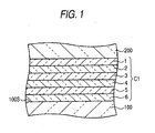
- Fig. 1 is a schematic cross-section view of an antireflection film C1 according to a first embodiment of the invention.
- the antireflection film C1 of Fig. 1 corresponds to first numerical examples ( Figs. 4 to 10 ) which will be described later.
- the antireflection film C1 is provided between an optical substrate 100 and an adhesion layer 200 and includes a multilayer film having first to sixth layers 1 to 6 which are laminated in order from one side of the adhesion layer 200.
- An equivalent refractive index of the entire antireflection film C1 is set to be lower than a refractive index of the optical substrate 100 and higher than that of the adhesive layer 200.
- a top surface 100S of the optical substrate 100 having the antireflection film C1 provided thereon is made of a planar surface.
- the top surface 100S may be made of a curved surface. That is, a lens having a spherical surface or an aspherical surface may be used as the optical substrate 100, and the antireflection film C1 may be provided on the spherical surface or aspherical surface of the lens.
- the adhesion layer 200 is made of an epoxy resin-based adhesive, for example, and has a refractive index of 1.45 to 1.60 at the d line.
- the first and third layers 1 and 3 are low refractive index layers made of a low refractive index material having a refractive index of 1.35 to 1.50 at the d line.
- the second, fourth, and sixth layers 2, 4, and 6 are middle refractive index layers made of a middle refractive index material having a refractive index of 1.55 to 1.85 at the d line.
- the fifth layer 5 is a high refractive index layer made of a high refractive index material having a refractive index, at the d line, that is a range of 1.70 to 2.50 and that is higher than that of the middle refractive index material.
- magnesium fluoride (MgF 2 ), silicon dioxide (SiO 2 ), aluminum fluoride (AlF 3 ), a mixture of them and a compound of them may be used.
- middle refractive index material praseodymium aluminate (PrAlO 3 ), lanthanum aluminate (La 2X Al 2Y O 3(X+Y) ), aluminum oxide (Al 2 O 3 ), germanium oxide (GeO 2 ), yttrium oxide (Y 2 O 3 ), a mixture of them and a compound of them may be used.
- lanthanum titanate LaTiO 3
- zirconium oxide ZrO 2
- titanium oxide TiO 2
- tantalum oxide Ti 2 O 5
- niobium oxide Nb 2 O 5
- hafnium oxide HfO 2
- cerium oxide CeO 2
- a mixture of them and a compound of them may be used.
- the first to sixth layers 1 to 6 are formed to satisfy the following conditional expressions (1) to (6).
- ⁇ 0 denotes a center wavelength (unit: nm)
- N1 to N6 denotes refractive indices of the first to sixth layers 1 to 6 at the center wavelength
- d1 to d6 denote physical thicknesses (unit: nm) of the first to sixth layers 1 to 6.
- the multilayer film including the first to sixth layers 1 to 6, which are laminated in order from the one side of the adhesion layer 200, has an intermediate refractive index between those of the optical substrate 100 and the adhesion layer 200, as a whole.
- the refractive indices of the second, fourth, and sixth layers 2, 4, and 6 are higher than those of the first and third layers 1 and 3 and lower than that of the fifth layer 5. Therefore, even if the refractive index Nd of the optical substrate 100 is around 2.0, reflectivity is sufficiently reduced in a wider band. Further, an optical thickness N ⁇ d is optimized by making the first to sixth layers 1 to 6 satisfy the respective conditional expressions (1) to (6),. Therefore, the above-described effect can be further increased.
- the antireflection film C1 when the antireflection film C1 is provided between the optical substrate 100 having the refractive index of 2.00 at the d line and the adhesion layer 200 having the refractive index of 1.50 to 1.60 at the d line, a reflectivity for normal incident light in at least a band of 400 to 700 nm can be reduced to less than 0.02%. Therefore, when the antireflection film C1 is applied to an optical system used in photographing cameras or broadcasting cameras, the occurrence of flare or ghost can be suppressed by reducing the reflection of incident light, and more excellent color chromaticity balance can be obtained.
- the reflectivity distribution of an antireflection film tends to be shifted in a short-wavelength side, as an incident angle increases. Therefore, according to the antireflection film C1 of this embodiment, the reflectivity can be reduced in a wider band than in the conventional antireflection film. Accordingly, the antireflection film can cope with incident light having a larger incident angle.
- the thickness of the multilayer film tends to easily decrease in a region where the curvature of the curved surface is relatively large, compared with the other regions where the curvature is relatively small.
- the antireflection film C1 of this embodiment sufficiently-low reflectivity is achieved in the wider band than in the conventional antireflection film. Therefore, even if a slight variation in the thickness occurs as described above, its excellent optical characteristic can be maintained.
- Fig. 2 is a schematic cross-section view of an antireflection film C2 according to a second embodiment of the invention.
- the antireflection film C2 of Fig. 2 corresponds to second numerical examples (shown in Figs. 10 to 16 ) which will be described later.
- the antireflection film C2 has the same configuration as that of the antireflection film C1 according to the first embodiment, except that the antireflection film C2 includes a multilayer film having eight layers in total. That is, the antireflection film C2 further includes seventh and eight layers 7 and 8 which are additionally laminated on the optical-substrate side of the sixth layer 6 in the reflection preventing layer C1. Therefore, the following descriptions will be mainly focused on the seventh and eight layers 7 and 8, and the descriptions of the other components will be omitted appropriately.
- the eighth layer 8 is a middle refractive index layer made of a middle refractive index material having a refractive index of 1.55 to 1.85 at the d line, like the second, fourth, and sixth layers.
- the seventh layer 7 is a high refractive index layer having a refractive index at the d line that is in a range of 1.70 to 2.50 and that is higher than that of the middle refractive index layer, like the fifth layer.
- the seventh and eighth layers 7 and 8 are formed to satisfy the following conditional expressions (7) and (8).
- the multilayer film including the first to eighth layers 1 to 8, which are laminated in order from the one side of the adhesion layer 200 has an intermediate refractive index between those of the optical substrate 100 and the adhesion layer 200, as a whole.
- the refractive indices of the second, fourth, sixth, and eighth layers 2, 4, 6, and 8 are higher than those of the first and third layers 1 and 3 and lower than those of the fifth and seventh layers 5 and 7. Therefore, even if the refractive index Nd of the optical substrate 100 is around 2.0, reflectivity is further sufficiently reduced in a wider band than in the antireflection film C1 according to the first embodiment.
- an optical thickness N ⁇ d is optimized by making the first to eighth layers 1 to 8 satisfy the respective conditional expressions (1) to (8). Therefore, the above-described effect can be further increased. Specifically, when the antireflection film C2 is provided between the optical substrate 100 having a refractive index Nd of 2.0 at the d line and the adhesion layer 200 having a refractive index of 1.50 to 1.60 at the d line, reflectivity of normal incidence light in at least a band of 400 to 950 nm can be reduced to less than 0.02%.
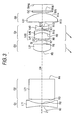
- Fig. 3 is a diagram showing the configuration of a zoom lens according to a third embodiment of the invention.
- the zoom lens includes the antireflection film C1 according to the first embodiment or the antireflection film C2 according to the second embodiment.
- a surface of a constituent element on the most object side being set as a first surface, and reference numerals are assigned to the respective constituent elements with sequentially increasing toward the image side (image formation side).
- a reference numeral Ri represents a curvature radius of an i-th surface.
- Reference numeral Di represents a surface separation between the i-th surface and the (i+1) th surface, on an optical axis Z1. Reference numeral Di is assigned only to surface separations which are changed in accordance with variation of power. Further, Fig. 3 shows lens arrangement at a wide-angle end.
- This zoom lens is mounted on an imaging apparatus such as a digital still camera, and first to fifth lens groups G1 to G5 are arranged in order from the object side along the optical axis Z1.
- the first and fourth lens groups G1 and G4 have a negative refractive power
- the third and fifth lens groups G3 and G5 have a positive refractive power.
- the second lens group G2 includes a prism L21 for bending a light path and does not have a refractive power.
- the third lens group G3 has an aperture stop St.
- an imaging element (not shown) is disposed on an image formation surface (imaging surface) Simg of the zoom lens.
- various optical components GC are disposed in accordance with the configuration of the camera having the lens mounted thereon.
- the optical components GC plane-shaped members such as a cover glass for protecting the imaging surface and various optical filters are disposed.
- the first, second, and fifth lens groups G1, G2, and G5 are always fixed during a zoom operation, while the third and fourth lens groups G3 and G4 are separately moved on the optical axis Z1 during the zoom operation.
- the third and fourth lens groups G3 and G4 are moved on the optical axis Z1 toward the object side, as indicated by arrows of Fig. 3 .
- the fourth lens group G4 has a cemented lens L40 composed of two lenses L41 and L42 and a negative lens L43.
- the lenses L41 and L42 are made of a glass material having a refractive index of 1.75 to 2.10.
- the antireflection film C1 shown in Fig. 1 (or the antireflection film C2 shown in Fig. 2 ) and the adhesion layer 200 are provided on an adhesion interface between the lenses L41 and L42.
- the antireflection films C1 (or the antireflection film C2) are provided on the image-side surface of the lens L41 and the object-side surface of the lens L42, respectively, and are bonded by the adhesion layer 200.
- the antireflection film C1 (or the antireflection film C2) is provided on the adhesion interface of the cemented lens L40, lower reflectivity can be obtained than in the conventional zoom lens even if the refractive indices Nd of the lenses L41 and L42 are around 2.0. Therefore, in the zoom lens of this embodiment including the cemented lens L40, the reflection of incident light is reduced, which makes it possible to suppress the occurrence of flare or ghost. Further, more excellent chromaticity balance can be obtained.
- the antireflection film C1 (or the antireflection film C2) is provided in the zoom lens, ghost in an infrared region can be suppressed while transmittance in a band from a near-infrared region to a visible region can be enhanced.
- the antireflection film C1 (or the antireflection film C2) may be provided only on the image-side surface of the lens L41 or the object-side surface of the lens L42. When the antireflection film is provided on both the surfaces, it is easy to obtain the above-described effect.
- Figs. 4 to 9 show first numerical examples (Examples 1-1 to 1-6).
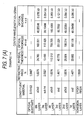
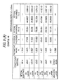
- Figs. 4(A) , 5(A) , 6(A) , 7(A) , 8(A) and 9(A) are tables' showing basic data of First Numerical Examples 1-1 to 1-6 corresponding to the antireflection film C1 shown in Fig. 1 .
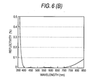
- Figs. 4(B) , 5(B) , 6(B) , 7(B) , 8(B) and 9(B) show the reflectivity distribution of Examples 1-1 to 1-6.
- Figs. 4 (A) , 5 (A) , 6 (A) , 7 (A) , 8 (A) and 9(A) show constituent materials, refractive indices N at the d line, physical thicknesses d (nm), and optical thicknesses (nm) of the respective layers.
- "sub-h4" indicates a substance H4 (made by Merck & Co., Inc., Germany) which mainly consists of LaTiO 3 .
- a center wavelength ⁇ 0 shown in the column of optical thickness N ⁇ d is set to 520 nm.
- the refractive indices N and the optical thicknesses N ⁇ d of the respective layers satisfy the conditional expressions (1) to (8).
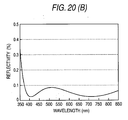
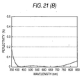
- Figs. 4(B) , 5(B) , 6(B) , 7(B) , 8(B) and 9(B) the vertical axis indicates reflectivity (%), and the horizontal axis indicates a wavelength ⁇ (nm) at the time of measurement.
- Figs. 4(B) , 5(B) , 6(B) , 7(B) , 8(B) and 9(B) show wavelength dependency of reflectivity (%) in the respective examples.
- Fig. 10 collectively shows the graphs of Figs. 4(B) , 5(B) , 6(B) , 7(B) , 8(B) and 9(B) .
- the reflectivity in a band of 400 to 650 nm is less than 0.02%.
- the refractive index N of the optical substrate 100 is equal to or more than 1.80
- the reflectivity in a band of 400 to 700 nm is less than 0.01%.
- Figs. 11 to 16 show second numerical examples (Examples 2-1 to 2-6).
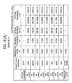
- Figs. 11(A) , 12(A) , 13(A) , 14(A) , 15(A) and 16(A) are tables showing basic data of Examples 2-1 to 2-6 corresponding to the antireflection film C2 shown in Fig. 2 .
- the center wavelength ⁇ 0 shown in the column of optical thickness N ⁇ d is set to 520 nm.
- the refractive indices N and the optical thicknesses N ⁇ d of the respective layers satisfy the conditional expressions (1) to (8).
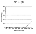
- Figs. 11(B) , 12(B) , 13(B) , 14(B) , 15 (B) and 16(B) show reflectivity distribution of Examples 2-1 to 2-6.
- Fig. 17 collectively shows the graphs of Figs. 11(B) , 12(B) , 13(B) , 14(B) , 15(B) and 16(B) .
- the reflectivity in a band of 400 to 900 nm is less than 0.02%.
- Example 2-6 that is, when the refractive index N of the optical substrate 100 is equal to or more than 1.80, the reflectivity in a band of 400 to 850 nm is less than 0.01%.
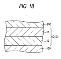
- Figs. 19 to 23 show Comparative Examples 1-1 to 1-5, which have an antireflection film C101 shown in Fig. 18 , as comparative examples with respect to the first and second numerical examples.
- the antireflection film C101 including first and second layers 11 and 12 has an intermediate refractive index between those of the optical substrate 100 and the adhesion layer 200, as a whole.
- Both of the first and second layers 11 and 12 are middle refractive index layers made of a middle refractive index material having a refractive index of 1.55 to 1.85 at the d line.
- the second layer 12 has a higher refractive index than that of the first layer 11.
- the first layer 11 is made of Al 2 O 3
- the second layer 12 is made of a substance M2 (made by Merck & Co., Inc., Germany), indicated by 'sub-m2', which mainly consists of lanthanum aluminate (La 2 O 3 ⁇ 3.3Al 2 O 3 ).
- the center wavelength ⁇ 0 shown in the column of optical thickness N ⁇ d is set to 520 nm.
- Figs. 19(B) , 20(B) , 21(B) , 22(B) and 23(B) show the reflectivity distribution of Comparative Examples 1-1 to 1-5.
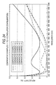
- Fig. 24 collectively shows the graphs of Figs. 19(B) , 20(B) , 21(B) , 22(B) and 23(B) .
- the reflectivity in a band of 400 to 650 nm largely exceeds 0.02% in any of the comparative examples, except Comparative Example 1-4 in which the refractive index of the optical substrate 100 is equal to 1.85. Even in Comparative Example 1-4, the reflectivity at a wavelength of 400 nm exceeds 0.03%, and the reflectivity at a wavelength of 700 nm exceeds 0.01%.
- the reflectivity distribution in the examples is significantly improved in comparison with that in the comparative examples having the two-layer structure. That is, according to the antireflection film of the embodiments of the invention, it is possible to sufficiently reduce the reflectivity in a wider band than in the conventional antireflection film. Furthermore, the reflectivity distribution can be sufficiently flattened.
- the invention has been described by exemplifying the embodiments and examples, the invention is not limited thereto. Various modifications may be made.
- the reflective indices and the optical thicknesses of the respective layers and the respective substrates are not limited to those of the numerical examples, but other values may be used.
- the materials composing the respective layers and the respective substrates are not limited to those of the numerical examples, but other materials may be used.
- each layer may be composed of a plurality of films, based on an equivalent film theory. That is, by laminating two kinds of refractive index films symmetrically, they may optically behave as a single layer.
Landscapes
- Physics & Mathematics (AREA)
- General Physics & Mathematics (AREA)
- Optics & Photonics (AREA)
- Chemical & Material Sciences (AREA)
- Inorganic Chemistry (AREA)
- Surface Treatment Of Optical Elements (AREA)
- Laminated Bodies (AREA)
- Lenses (AREA)
Abstract
Description
- The invention relates to an antireflection film that is formed on a bonded surface between optical members such as a lens and a filter and exerts an antireflection effect with respect to light in a predetermined band; an optical element; and an optical system including the same.
- In general, an imaging apparatus such as a photographing camera and a broadcasting camera has a plurality of optical members, such as lenses, prisms, and filters, disposed on its light path. When the optical members are bonded to each other through an adhesion layer made of a transparent resin, a part of incident light may be reflected at the adhesion interface between the adhesion layer and the optical members, thereby causing flare or ghost appearing on an image. Further, reflectivity at the adhesion interface has distribution depending on the wavelength of the incident light, and also shows different wavelength dependency in accordance with constituent materials of the respective optical members. Therefore, chromaticity balance is degraded, and it is necessary to adjust the white balance of the entire imaging apparatus.
- Accordingly, an antireflection film is provided between the optical members and the adhesion layer.
- The antireflection film is a multilayer film in which a plurality of dielectric films having different refractive indices from each other are combined.
JP 2001-74903 A JP 2006-284656 A - Recently, however, an optical system in which a glass having a high refractive index Nd of around 2.0 with respect to d line (wavelength λ = 587.56 nm) is frequently used. In the antireflection films disclosed in
JP 2001-74903 A JP 2006-284656 A - The invention has been made in view of the above circumstances, and provides an antireflection film that has lower reflectivity in a sufficiently wide band even if optical members having higher refractive indices are bonded and provides an optical element and an optical system including the antireflection film.
- According to an aspect of the invention, an antireflection film is provided between an optical member and an adhesion layer and includes a multilayer film having at least first to sixth layers that are laminated in order from the adhesion-layer side. An equivalent refractive index of the multilayer film as a whole is lower than that of the optical member and higher than that of the adhesion layer. Also, refractive indices of the second, fourth and sixth layers are higher than those of the first and third layers and lower than that of the fifth layer. Furthermore, according to another aspect of the invention, in an optical element, an optical member having a refractive index of 1.75 to 2.10 at d line and another optical member are bonded to each other through an adhesion layer. The above antireflection film is provided between the optical member and the adhesion layer. According to further another aspect of the invention, an optical system includes the above optical element.
- In the antireflection film, the optical element and the optical system, the multilayer film having the at least first to sixth layers in order from the one side of the adhesion layer has an intermediate refractive index between that of the optical member and that of the adhesion layer. Refractive indices of the second, fourth and sixth layers are higher than those of the first and third layers and lower than that of the fifth layer. Therefore, even if a refractive index Nd of the substrate exceeds 2.0, a reflectivity distribution can be sufficiently reduced in a wider band.
- Also, in the antireflection film, the optical element an d optical system, the following conditional expressions (1) to (6) may be satisfied:


where λ0 denotes a center wavelength, N1 to N6 denote refractive indices of the first to sixth layers at the center wavelength λ0, and d1 to d6 denote physical thicknesses of the first to sixth layers. - In the antireflection film, the optical element and optical system, the multilayer film may further include seventh and eighth layers that are laminated on an optical-member side of the sixth layer. A refractive index of the seventh layer is higher than those of the first to fourth and sixth layers. A refractive index of the eighth layer is higher than those of the first and third layers and is lower than those of the fifth and seventh layers. In this case, the following conditional expressions (7) and (8) may be satisfied:


where λ0 denotes the center wavelength, N7 and N8 denote refractive indices of the seventh and eighth layers at the center wavelength λ0, and d7 and d8 denote physical thicknesses of the seventh and eighth layers. - In the antireflection film, the optical element and optical system, the first and third layers may be made of a low refractive index material having refractive index of 1.35 to 1.50 at d line. The second, fourth, sixth, and eighth layers may be made of a middle refractive index material having a refractive index of 1.55 to 1.85 at the d line. The fifth and seventh layers may be made of a high refractive index material having a refractive index, at the d line, that is in a range of 1.70 to 2.50 and that is higher than that of the middle refractive index material.
- In the antireflection film, the optical element and the optical system, the low refractive index material may include at least one of MgF2, SiO2 and AlF3. The middle refractive index material may include at least one of PrAlO3, La2XAl2YO3(X+Y), Al2O3, GeO2 and Y2O3. The high refractive index material may include at least one of LaTi2, ZrO2, TiO2, Ta2O5, Nb2O5, HfO2, and CeO2.
- In the antireflection film, the optical element and the optical system, the other optical member may have a refractive index of 1.75 to 2.10 at the d line. Another antireflection film may be provided between the other optical member and the adhesion layer. The other antireflection film may include a multilayer film having at least ninth to fourteenth layers that are disposed between the other optical member and the adhesion layer. The ninth to fourteenth layers are laminated in order from the other side of the adhesion layer. An equivalent refractive index of the entire multilayer film of the other antireflection film may be lower than that of the other optical member and higher than that of the adhesion layer. Refractive indices of the tenth, twelfth and fourteenth layers may be higher than those of the ninth and eleventh layers and lower than that of the thirteenth layer.
- With the above antireflection film, the antireflection film has the intermediate refractive index between that of the optical member and that of the adhesion layer and includes the multilayer film having the first to sixth layers. In the multilayer film, the refractive indices of the second, fourth, and sixth layers are set to be higher than those of the first and third layers and lower than that of the fifth layer. Therefore, even if the refractive index of the optical member is around 2.0, low reflectivity can be exhibited in a sufficiently wide band. Accordingly, when an optical element (such as cemented lens or the like) using the antireflection film is applied to an optical system mounted on photographing cameras or broadcasting cameras, it is possible to suppress the occurrence of flare or ghost and to obtain more excellent chromaticity balance.
-
-
Fig. 1 is a schematic cross-section view of an antireflection film according to a first embodiment of the invention. -
Fig. 2 is a schematic cross-section view of an antireflection film according to a second embodiment of the invention. -
Fig. 3 is a cross-section view of a zoom lens according to a third embodiment of the invention. -
Figs. 4A and4B show basic data and reflectivity distribution of Example 1-1 corresponding to the antireflection film shown inFig. 1 . -
Figs. 5A and5B show basic data and reflectivity distribution of Example 1-2 corresponding to the antireflection film shown inFig. 1 . -
Figs. 6A and6B show basic data and reflectivity distribution of Example 1-3 corresponding to the antireflection film shown inFig. 1 . -
Figs. 7A and7B show basic data and reflectivity distribution of Example 1-4 corresponding to the antireflection film shown inFig. 1 . -
Figs. 8A and8B show basic data and reflectivity distribution of Example 1-5 corresponding to the antireflection film shown inFig. 1 . -
Figs. 9A and9B show basic data and reflectivity distribution of Example 1-2 corresponding to the antireflection film shown inFig. 1 . -
Fig. 10 is a characteristic diagram collectively showing all the reflectivity distributions of Examples 1-1 to 1-6 shown inFigs. 5 to 9 . -
Figs. 11A and11B show basic data and reflectivity distribution of Example 2-1 corresponding to the antireflection film shown inFig. 2 . -
Figs. 12A and12B show basic data and reflectivity distribution of Example 2-2 corresponding to the antireflection film shown inFig. 2 . -
Figs. 13A and13B show basic data and reflectivity distribution of Example 2-3 corresponding to the antireflection film shown inFig. 2 . -
Figs. 14A and14B show basic data and reflectivity distribution of Example 2-4 corresponding to the antireflection film shown inFig. 2 . -
Figs. 15A and15B show basic data and reflectivity distribution of Example 2-5 corresponding to the antireflection film shown inFig. 2 . -
Figs. 16A and16B show basic data and reflectivity distribution of Example 2-6 corresponding to the antireflection film shown inFig. 2 . -
Fig. 17 is a characteristic diagram collectively showing reflectivity distribution of Examples 2-1 to 2-6 shown inFigs. 11 to 16 . -
Fig. 18 is a cross-section view of an antireflection film as a comparative example. -
Figs. 19A and19B show basic data and reflectivity distribution of Comparative Example 1-1 corresponding to the antireflection film shown inFig. 18 . -
Figs. 20A and20B show basic data and reflectivity distribution of Comparative Example 1-2 corresponding to the antireflection film shown inFig. 18 . -
Figs. 21A and21B show basic data and reflectivity distribution of Comparative Example 1-3 corresponding to the antireflection film shown inFig. 18 . -
Figs. 22A and22B show basic data and reflectivity distribution of Comparative Example 1-4 corresponding to the antireflection film shown inFig. 18 . -
Figs. 23A and23B show basic data and reflectivity distribution of Comparative Example 1-5 corresponding to the antireflection film shown inFig. 18 . -
Figs. 24A and 24B are characteristic diagrams collectively showing all the reflectivity distributions of Comparative Examples 1-1 to 1-5 shown inFigs. 19 to 23 . - Hereinafter, embodiments of the invention will be described in detail with reference to the accompanying drawings.
-
Fig. 1 is a schematic cross-section view of an antireflection film C1 according to a first embodiment of the invention. The antireflection film C1 ofFig. 1 corresponds to first numerical examples (Figs. 4 to 10 ) which will be described later. - The antireflection film C1 is provided between an
optical substrate 100 and anadhesion layer 200 and includes a multilayer film having first tosixth layers 1 to 6 which are laminated in order from one side of theadhesion layer 200. An equivalent refractive index of the entire antireflection film C1 is set to be lower than a refractive index of theoptical substrate 100 and higher than that of theadhesive layer 200. InFig. 1 , atop surface 100S of theoptical substrate 100 having the antireflection film C1 provided thereon is made of a planar surface. However, the invention is not limited thereto. Thetop surface 100S may be made of a curved surface. That is, a lens having a spherical surface or an aspherical surface may be used as theoptical substrate 100, and the antireflection film C1 may be provided on the spherical surface or aspherical surface of the lens. - The
optical substrate 100 is made of a transparent material such as glass or a crystalline material. Specifically, it is preferable that theoptical substrate 100 is made of SF-14, SF6 (made by Schott AG, Germany), LASF-N17, S-NPH2, S-TIH53, or S-LAH79 (made by OHARA Inc.), which has a refractive index less of 1.75 to 2.10 at d line (wavelength λ = 587.56 nm). - The
adhesion layer 200 is made of an epoxy resin-based adhesive, for example, and has a refractive index of 1.45 to 1.60 at the d line. - The first and
third layers sixth layers fifth layer 5 is a high refractive index layer made of a high refractive index material having a refractive index, at the d line, that is a range of 1.70 to 2.50 and that is higher than that of the middle refractive index material. - As the low refractive index material, magnesium fluoride (MgF2), silicon dioxide (SiO2), aluminum fluoride (AlF3), a mixture of them and a compound of them may be used. As the middle refractive index material, praseodymium aluminate (PrAlO3), lanthanum aluminate (La2XAl2YO3(X+Y)), aluminum oxide (Al2O3), germanium oxide (GeO2), yttrium oxide (Y2O3), a mixture of them and a compound of them may be used. As the high refractive index material, lanthanum titanate (LaTiO3), zirconium oxide (ZrO2), titanium oxide (TiO2), tantalum oxide (Ta2O5), niobium oxide (Nb2O5), hafnium oxide (HfO2), cerium oxide (CeO2), a mixture of them and a compound of them may be used.
- Preferably, the first to
sixth layers 1 to 6 are formed to satisfy the following conditional expressions (1) to (6). Here, λ0 denotes a center wavelength (unit: nm), N1 to N6 denotes refractive indices of the first tosixth layers 1 to 6 at the center wavelength, and d1 to d6 denote physical thicknesses (unit: nm) of the first tosixth layers 1 to 6.




- With the antireflection film C1 according to this embodiment, the multilayer film including the first to
sixth layers 1 to 6, which are laminated in order from the one side of theadhesion layer 200, has an intermediate refractive index between those of theoptical substrate 100 and theadhesion layer 200, as a whole. The refractive indices of the second, fourth, andsixth layers third layers fifth layer 5. Therefore, even if the refractive index Nd of theoptical substrate 100 is around 2.0, reflectivity is sufficiently reduced in a wider band. Further, an optical thickness N·d is optimized by making the first tosixth layers 1 to 6 satisfy the respective conditional expressions (1) to (6),. Therefore, the above-described effect can be further increased. Specifically, when the antireflection film C1 is provided between theoptical substrate 100 having the refractive index of 2.00 at the d line and theadhesion layer 200 having the refractive index of 1.50 to 1.60 at the d line, a reflectivity for normal incident light in at least a band of 400 to 700 nm can be reduced to less than 0.02%. Therefore, when the antireflection film C1 is applied to an optical system used in photographing cameras or broadcasting cameras, the occurrence of flare or ghost can be suppressed by reducing the reflection of incident light, and more excellent color chromaticity balance can be obtained. - In general, the reflectivity distribution of an antireflection film tends to be shifted in a short-wavelength side, as an incident angle increases. Therefore, according to the antireflection film C1 of this embodiment, the reflectivity can be reduced in a wider band than in the conventional antireflection film. Accordingly, the antireflection film can cope with incident light having a larger incident angle.
- Further, when the multilayer film is formed on a curved surface such as a lens surface, the thickness of the multilayer film tends to easily decrease in a region where the curvature of the curved surface is relatively large, compared with the other regions where the curvature is relatively small. According to the antireflection film C1 of this embodiment, however, sufficiently-low reflectivity is achieved in the wider band than in the conventional antireflection film. Therefore, even if a slight variation in the thickness occurs as described above, its excellent optical characteristic can be maintained.
-
Fig. 2 is a schematic cross-section view of an antireflection film C2 according to a second embodiment of the invention. The antireflection film C2 ofFig. 2 corresponds to second numerical examples (shown inFigs. 10 to 16 ) which will be described later. - The antireflection film C2 has the same configuration as that of the antireflection film C1 according to the first embodiment, except that the antireflection film C2 includes a multilayer film having eight layers in total. That is, the antireflection film C2 further includes seventh and eight
layers sixth layer 6 in the reflection preventing layer C1. Therefore, the following descriptions will be mainly focused on the seventh and eightlayers - The
eighth layer 8 is a middle refractive index layer made of a middle refractive index material having a refractive index of 1.55 to 1.85 at the d line, like the second, fourth, and sixth layers. On the contrary, theseventh layer 7 is a high refractive index layer having a refractive index at the d line that is in a range of 1.70 to 2.50 and that is higher than that of the middle refractive index layer, like the fifth layer. - Preferably, the seventh and
eighth layers 

- According to the antireflection film C2 of this embodiment, the multilayer film including the first to
eighth layers 1 to 8, which are laminated in order from the one side of theadhesion layer 200, has an intermediate refractive index between those of theoptical substrate 100 and theadhesion layer 200, as a whole. Further, the refractive indices of the second, fourth, sixth, andeighth layers third layers seventh layers optical substrate 100 is around 2.0, reflectivity is further sufficiently reduced in a wider band than in the antireflection film C1 according to the first embodiment. Furthermore, an optical thickness N·d is optimized by making the first toeighth layers 1 to 8 satisfy the respective conditional expressions (1) to (8). Therefore, the above-described effect can be further increased. Specifically, when the antireflection film C2 is provided between theoptical substrate 100 having a refractive index Nd of 2.0 at the d line and theadhesion layer 200 having a refractive index of 1.50 to 1.60 at the d line, reflectivity of normal incidence light in at least a band of 400 to 950 nm can be reduced to less than 0.02%. -
Fig. 3 is a diagram showing the configuration of a zoom lens according to a third embodiment of the invention. The zoom lens includes the antireflection film C1 according to the first embodiment or the antireflection film C2 according to the second embodiment. - In
Fig. 3 , a surface of a constituent element on the most object side being set as a first surface, and reference numerals are assigned to the respective constituent elements with sequentially increasing toward the image side (image formation side). A reference numeral Ri represents a curvature radius of an i-th surface. Reference numeral Di represents a surface separation between the i-th surface and the (i+1) th surface, on an optical axis Z1. Reference numeral Di is assigned only to surface separations which are changed in accordance with variation of power. Further,Fig. 3 shows lens arrangement at a wide-angle end. - This zoom lens is mounted on an imaging apparatus such as a digital still camera, and first to fifth lens groups G1 to G5 are arranged in order from the object side along the optical axis Z1. The first and fourth lens groups G1 and G4 have a negative refractive power, and the third and fifth lens groups G3 and G5 have a positive refractive power. The second lens group G2 includes a prism L21 for bending a light path and does not have a refractive power. Further, the third lens group G3 has an aperture stop St.
- On an image formation surface (imaging surface) Simg of the zoom lens, an imaging element (not shown) is disposed. Between the fifth lens group G5 and the imaging surface Simg, various optical components GC are disposed in accordance with the configuration of the camera having the lens mounted thereon. As the optical components GC, plane-shaped members such as a cover glass for protecting the imaging surface and various optical filters are disposed.
- In this zoom lens, the first, second, and fifth lens groups G1, G2, and G5 are always fixed during a zoom operation, while the third and fourth lens groups G3 and G4 are separately moved on the optical axis Z1 during the zoom operation. As power is varied from the wide-angle end to the telephoto end, the third and fourth lens groups G3 and G4 are moved on the optical axis Z1 toward the object side, as indicated by arrows of
Fig. 3 . - The fourth lens group G4 has a cemented lens L40 composed of two lenses L41 and L42 and a negative lens L43. The lenses L41 and L42 are made of a glass material having a refractive index of 1.75 to 2.10. Although not shown in
Fig. 3 , the antireflection film C1 shown inFig. 1 (or the antireflection film C2 shown inFig. 2 ) and theadhesion layer 200 are provided on an adhesion interface between the lenses L41 and L42. Specifically, the antireflection films C1 (or the antireflection film C2) are provided on the image-side surface of the lens L41 and the object-side surface of the lens L42, respectively, and are bonded by theadhesion layer 200. - Since the antireflection film C1 (or the antireflection film C2) is provided on the adhesion interface of the cemented lens L40, lower reflectivity can be obtained than in the conventional zoom lens even if the refractive indices Nd of the lenses L41 and L42 are around 2.0. Therefore, in the zoom lens of this embodiment including the cemented lens L40, the reflection of incident light is reduced, which makes it possible to suppress the occurrence of flare or ghost. Further, more excellent chromaticity balance can be obtained.
- Furthermore, since the antireflection film C1 (or the antireflection film C2) is provided in the zoom lens, ghost in an infrared region can be suppressed while transmittance in a band from a near-infrared region to a visible region can be enhanced.
- The antireflection film C1 (or the antireflection film C2) may be provided only on the image-side surface of the lens L41 or the object-side surface of the lens L42. When the antireflection film is provided on both the surfaces, it is easy to obtain the above-described effect.
- Next, specific numerical examples of the antireflection film according to the embodiments of the invention will be described. Further, the reflectivities in these examples indicate values when light is vertically incident.
-
Figs. 4 to 9 show first numerical examples (Examples 1-1 to 1-6).Figs. 4(A) ,5(A) ,6(A) ,7(A) ,8(A) and9(A) are tables' showing basic data of First Numerical Examples 1-1 to 1-6 corresponding to the antireflection film C1 shown inFig. 1 . Also,Figs. 4(B) ,5(B) ,6(B) ,7(B) ,8(B) and9(B) show the reflectivity distribution of Examples 1-1 to 1-6. -
Figs. 4 (A) ,5 (A) ,6 (A) ,7 (A) ,8 (A) and9(A) show constituent materials, refractive indices N at the d line, physical thicknesses d (nm), and optical thicknesses (nm) of the respective layers. In the column of constituent material, "sub-h4" indicates a substance H4 (made by Merck & Co., Inc., Germany) which mainly consists of LaTiO3. Also, a center wavelength λ0 shown in the column of optical thickness N·d is set to 520 nm. As is clear from the respective figures, the refractive indices N and the optical thicknesses N·d of the respective layers satisfy the conditional expressions (1) to (8). Meanwhile, inFigs. 4(B) ,5(B) ,6(B) ,7(B) ,8(B) and9(B) , the vertical axis indicates reflectivity (%), and the horizontal axis indicates a wavelength λ (nm) at the time of measurement.Figs. 4(B) ,5(B) ,6(B) ,7(B) ,8(B) and9(B) show wavelength dependency of reflectivity (%) in the respective examples.Fig. 10 collectively shows the graphs ofFigs. 4(B) ,5(B) ,6(B) ,7(B) ,8(B) and9(B) . As shown in the respective figures, the reflectivity in a band of 400 to 650 nm is less than 0.02%. Particularly, except Example 1-6, that is, if the refractive index N of theoptical substrate 100 is equal to or more than 1.80, the reflectivity in a band of 400 to 700 nm is less than 0.01%. -
Figs. 11 to 16 show second numerical examples (Examples 2-1 to 2-6). -
Figs. 11(A) ,12(A) ,13(A) ,14(A) ,15(A) and16(A) are tables showing basic data of Examples 2-1 to 2-6 corresponding to the antireflection film C2 shown inFig. 2 . The center wavelength λ0 shown in the column of optical thickness N·d is set to 520 nm. As shown in the respective figures, the refractive indices N and the optical thicknesses N·d of the respective layers satisfy the conditional expressions (1) to (8). - Meanwhile,
Figs. 11(B) ,12(B) ,13(B) ,14(B) ,15 (B) and16(B) show reflectivity distribution of Examples 2-1 to 2-6.Fig. 17 collectively shows the graphs ofFigs. 11(B) ,12(B) ,13(B) ,14(B) ,15(B) and16(B) . As shown in the respective figures, the reflectivity in a band of 400 to 900 nm is less than 0.02%. Particularly, except Example 2-6, that is, when the refractive index N of theoptical substrate 100 is equal to or more than 1.80, the reflectivity in a band of 400 to 850 nm is less than 0.01%. -
Figs. 19 to 23 show Comparative Examples 1-1 to 1-5, which have an antireflection film C101 shown inFig. 18 , as comparative examples with respect to the first and second numerical examples. InFig. 18 , the antireflection film C101 including first andsecond layers optical substrate 100 and theadhesion layer 200, as a whole. Both of the first andsecond layers second layer 12 has a higher refractive index than that of thefirst layer 11.Figs. 19(A) ,20(A) ,21(A) ,22(A) and23(A) are tables showing specific basic data of Comparative Examples 1-1 to 1-5. Thefirst layer 11 is made of Al2O3, and thesecond layer 12 is made of a substance M2 (made by Merck & Co., Inc., Germany), indicated by 'sub-m2', which mainly consists of lanthanum aluminate (La2O3·3.3Al2O3). Further, the center wavelength λ0 shown in the column of optical thickness N·d is set to 520 nm. - Meanwhile,
Figs. 19(B) ,20(B) ,21(B) ,22(B) and23(B) show the reflectivity distribution of Comparative Examples 1-1 to 1-5.Fig. 24 collectively shows the graphs ofFigs. 19(B) ,20(B) ,21(B) ,22(B) and23(B) . - As is clear from the respective figures, the reflectivity in a band of 400 to 650 nm largely exceeds 0.02% in any of the comparative examples, except Comparative Example 1-4 in which the refractive index of the
optical substrate 100 is equal to 1.85. Even in Comparative Example 1-4, the reflectivity at a wavelength of 400 nm exceeds 0.03%, and the reflectivity at a wavelength of 700 nm exceeds 0.01%. - Through the above-described basic data and the respective reflectivity distribution figures, it can be found that the reflectivity distribution in the examples is significantly improved in comparison with that in the comparative examples having the two-layer structure. That is, according to the antireflection film of the embodiments of the invention, it is possible to sufficiently reduce the reflectivity in a wider band than in the conventional antireflection film. Furthermore, the reflectivity distribution can be sufficiently flattened.
- Although the invention has been described by exemplifying the embodiments and examples, the invention is not limited thereto. Various modifications may be made. For example, the reflective indices and the optical thicknesses of the respective layers and the respective substrates are not limited to those of the numerical examples, but other values may be used. Further, the materials composing the respective layers and the respective substrates are not limited to those of the numerical examples, but other materials may be used.
- Furthermore, each layer may be composed of a plurality of films, based on an equivalent film theory. That is, by laminating two kinds of refractive index films symmetrically, they may optically behave as a single layer.
Claims (10)
- An optical element comprising:an optical member;another optical member;an adhesion layer, wherein the optical member and the other optical member are bonded to each other through the adhesive layer; andan antireflection film including a multilayer film having at least first to sixth layers that are disposed between the optical member and the adhesion layer, the first to sixth layers being laminated in order from one side of the adhesion layer, whereinan equivalent refractive index of the entire multilayer film is lower than that of the optical member and higher than that of the adhesion layer, andrefractive indices of the second, fourth and sixth layers are higher than those of the first and third layers and lower than that of the fifth layer.
- The optical element to claim 1, wherein
the following conditional expressions (1) to (6) are satisfied:


where λ0 denotes a center wavelength, N1 to N6 denote refractive indices of the first to sixth layers at the center wavelength λ0, and d1 to d6 denote physical thicknesses of the first to sixth layers. - The optical element according to any one of claims 1 to 2, wherein
the first and third layers are made of a low refractive index material having refractive index of 1.35 to 1.50 at d line,
the second, fourth, and sixth layers are made of a middle refractive index material having a refractive index of 1.55 to 1.85 at the d line, and
the fifth layer is made of a high refractive index material having a refractive index, at the d line, that is in a range of 1.70 to 2.50 and that is higher than that of the middle refractive index material. - The optical element according to claim 1, wherein
the multilayer film further comprises seventh and eighth layers that are laminated on an optical-member side of the sixth layer,
a refractive index of the seventh layer is higher than those of the first to fourth and sixth layers, and
a refractive index of the eighth layer is higher than those of the first and third layers and is lower than those of the fifth and seventh layers. - The optical element according to claim 4, wherein
the following conditional expressions (7) and (8) are satisfied:

where λ0 denotes the center wavelength, N7 and N8 denote refractive indices of the seventh and eighth layers at the center wavelength λ0, and d7 and d8 denote physical thicknesses of the seventh and eighth layers. - The optical element according to any one of claims 4 to 5, wherein
the first and third layers are made of a low refractive index material having a refractive index of 1.35 to 1.50 at d line,
the second, fourth, sixth, and eighth layers are made of a middle refractive index material having a refractive index of 1.55 to 1.85 at the d line, and
the fifth and seventh layers are made of a high refractive index material having a refractive index, at the d line, that is in a range of 1.70 to 2.50 and that is higher than that of the middle refractive index material - The optical element according to any one of claims 3 and 6, wherein
the low refractive index material includes at least one of MgF2, SiO2 and AlF3,
the middle refractive index material includes at least one of PrAlO3, La2XAl2YO3(X+Y), Al2O3, GeO2 and Y2O3, and
the high refractive index material includes at least one of LaTi2, ZrO2, TiO2, Ta2O5, Nb2O5, HfO2, and CeO2. - The optical element according to any one of claims 1 to 7, wherein
the optical member has a refractive index of 1.75 to 2.10 at the d line, and
the adhesion layer has a refractive index of 1.45 to 1.60 at the d line. - The optical element according to any one of claims 1 to 7, wherein
the other optical member has a refractive index of 1.75 to 2.10 at the d line, and
the optical element further comprising:another antireflection film between the other optical member and the adhesion layer, whereinthe other antireflection film includes a multilayer film having at least ninth to fourteenth layers that are disposed between the other optical member and the adhesion layer, the ninth to fourteenth layers being laminated in order from the other side of the adhesion layer, whereinan equivalent refractive index of the entire multilayer film of the other antireflection film is lower than that of the other optical member and higher than that of the adhesion layer, andrefractive indices of the tenth, twelfth and fourteenth layers are higher than those of the ninth and eleventh layers and lower than that of the thirteenth layer. - An optical system comprising the optical element according to any one of claims 1 to 9.
Applications Claiming Priority (1)
| Application Number | Priority Date | Filing Date | Title |
|---|---|---|---|
| JP2007074530A JP4958594B2 (en) | 2007-03-22 | 2007-03-22 | Antireflection film, optical element and optical system |
Publications (2)
| Publication Number | Publication Date |
|---|---|
| EP1972966A2 true EP1972966A2 (en) | 2008-09-24 |
| EP1972966A3 EP1972966A3 (en) | 2008-10-22 |
Family
ID=39535718
Family Applications (1)
| Application Number | Title | Priority Date | Filing Date |
|---|---|---|---|
| EP08002220A Withdrawn EP1972966A3 (en) | 2007-03-22 | 2008-02-06 | Antireflection film, optical element and optical system |
Country Status (5)
| Country | Link |
|---|---|
| US (1) | US7791803B2 (en) |
| EP (1) | EP1972966A3 (en) |
| JP (1) | JP4958594B2 (en) |
| KR (1) | KR100972569B1 (en) |
| CN (1) | CN101271166B (en) |
Cited By (3)
| Publication number | Priority date | Publication date | Assignee | Title |
|---|---|---|---|---|
| TWI395971B (en) * | 2009-01-09 | 2013-05-11 | Hon Hai Prec Ind Co Ltd | Anti-reflection film and optical element with same |
| WO2022090228A1 (en) * | 2020-10-27 | 2022-05-05 | Essilor International | Optical article to provide vision correction for devices using eye tracking device |
| EP3974876A4 (en) * | 2020-05-21 | 2022-11-16 | Dexerials Corporation | ANTI-REFLECTIVE FILM |
Families Citing this family (32)
| Publication number | Priority date | Publication date | Assignee | Title |
|---|---|---|---|---|
| JP5096253B2 (en) * | 2008-07-28 | 2012-12-12 | 富士フイルム株式会社 | Zoom lens, imaging device, and mobile phone |
| JP5197274B2 (en) * | 2008-09-26 | 2013-05-15 | 日東光学株式会社 | Optical member manufacturing method and optical member |
| JP5455387B2 (en) * | 2009-01-30 | 2014-03-26 | キヤノン株式会社 | Film and optical lens formed on outer peripheral surface of lens |
| JP2010198735A (en) * | 2009-02-20 | 2010-09-09 | Fujifilm Corp | Optical member and organic electroluminescent display device equipped with the same |
| JP5373514B2 (en) * | 2009-09-11 | 2013-12-18 | 富士フイルム株式会社 | Zoom lens and imaging device |
| JP5529475B2 (en) * | 2009-09-11 | 2014-06-25 | 富士フイルム株式会社 | Zoom lens and imaging device |
| JP5373515B2 (en) * | 2009-09-11 | 2013-12-18 | 富士フイルム株式会社 | Zoom lens and imaging device |
| CN101806927B (en) * | 2010-02-25 | 2013-09-11 | 海洋王照明科技股份有限公司 | High-reflecting film and preparation method thereof |
| DE102010048088A1 (en) * | 2010-10-01 | 2012-04-05 | Carl Zeiss Vision Gmbh | Optical lens with scratch-resistant anti-reflection coating |
| CN102029739A (en) * | 2010-10-09 | 2011-04-27 | 杭州科汀光学技术有限公司 | Optical multi-layer film with high heat conduction and low strain |
| JP5893271B2 (en) * | 2011-06-10 | 2016-03-23 | オリンパス株式会社 | Antireflection film, optical system, and optical apparatus |
| TWI509292B (en) | 2011-09-07 | 2015-11-21 | Hon Hai Prec Ind Co Ltd | Lens and lens module having lens |
| CN102999196B (en) * | 2011-09-09 | 2016-04-06 | 宸鸿科技(厦门)有限公司 | Touch-control stacked structure |
| CN102998724B (en) * | 2011-09-13 | 2016-05-11 | 鸿富锦精密工业(深圳)有限公司 | Eyeglass and there is the camera lens module of this eyeglass |
| CN103176225A (en) * | 2011-12-22 | 2013-06-26 | 凤凰光学(上海)有限公司 | High-strength antireflection film system structure |
| JP2013174787A (en) * | 2012-02-27 | 2013-09-05 | Panasonic Corp | Optical member |
| JP6202785B2 (en) * | 2012-05-30 | 2017-09-27 | オリンパス株式会社 | Antireflection film, optical system, optical apparatus, and method for forming antireflection film |
| JP6116337B2 (en) * | 2013-04-24 | 2017-04-19 | 株式会社大真空 | Optical device |
| CN104297887A (en) * | 2013-07-17 | 2015-01-21 | 玉晶光电(厦门)有限公司 | Photographic lens and gasket for same |
| JP6385117B2 (en) * | 2014-04-11 | 2018-09-05 | キヤノン株式会社 | Optical element and optical system having the same |
| JP6314627B2 (en) * | 2014-04-21 | 2018-04-25 | リコーイメージング株式会社 | Antireflection film and optical component having the same |
| WO2016035710A1 (en) * | 2014-09-02 | 2016-03-10 | コニカミノルタ株式会社 | Prism unit and projector |
| DE102015100091A1 (en) * | 2015-01-07 | 2016-07-07 | Rodenstock Gmbh | Layer system and optical element with a layer system |
| JP6582465B2 (en) * | 2015-03-17 | 2019-10-02 | コニカミノルタ株式会社 | Projection lens and projector |
| US9960199B2 (en) | 2015-12-29 | 2018-05-01 | Viavi Solutions Inc. | Dielectric mirror based multispectral filter array |
| US9923007B2 (en) | 2015-12-29 | 2018-03-20 | Viavi Solutions Inc. | Metal mirror based multispectral filter array |
| JP2019117311A (en) * | 2017-12-27 | 2019-07-18 | マルミ光機株式会社 | Nd filter and manufacturing method therefor |
| US10705273B2 (en) * | 2018-03-26 | 2020-07-07 | Raytheon Company | Multispectral interference coating with diamond-like carbon (DLC) film |
| CN108957608A (en) * | 2018-07-06 | 2018-12-07 | 福建福晶科技股份有限公司 | A kind of design and its preparation of wide angle near-infrared hot mirror |
| CN112612113B (en) * | 2020-12-29 | 2023-09-19 | 福建福光天瞳光学有限公司 | Day and night confocal lens with large aperture of 3.9mm and imaging method thereof |
| TWI835646B (en) * | 2023-05-10 | 2024-03-11 | 澤米科技股份有限公司 | Optical component structure with a lanthanide compound layer |
| CN119065115B (en) * | 2024-11-05 | 2025-09-23 | 理湃光晶(苏州)科技有限公司 | Eyepieces for near-eye display devices |
Citations (2)
| Publication number | Priority date | Publication date | Assignee | Title |
|---|---|---|---|---|
| JP2001074903A (en) | 1999-09-03 | 2001-03-23 | Nikon Corp | Antireflection film and optical element |
| JP2006284656A (en) | 2005-03-31 | 2006-10-19 | Fujinon Corp | Light antireflection optical system and imaging optical system |
Family Cites Families (17)
| Publication number | Priority date | Publication date | Assignee | Title |
|---|---|---|---|---|
| DE1936091A1 (en) * | 1969-07-16 | 1971-01-28 | Rodenstock Optik G | Cemented optical assembly eg compound lens |
| US3809459A (en) * | 1972-10-13 | 1974-05-07 | Asahi Optical Co Ltd | Antireflection coating for an inner surface of cemented lenses |
| JPS5390316A (en) | 1977-01-20 | 1978-08-09 | Nippon Chemical Ind | Reflectionnproof film |
| JPS62124503A (en) * | 1985-11-25 | 1987-06-05 | Minolta Camera Co Ltd | Multi-layered antireflection film |
| JPH05100104A (en) * | 1991-10-04 | 1993-04-23 | Olympus Optical Co Ltd | Composite type optical parts |
| JPH05215906A (en) * | 1992-01-31 | 1993-08-27 | Asahi Optical Co Ltd | Multilayer polarization separation film |
| JP3113371B2 (en) * | 1992-01-31 | 2000-11-27 | 旭光学工業株式会社 | Multi-layer anti-reflective coating |
| US5532871A (en) * | 1992-11-25 | 1996-07-02 | Canon Kabushiki Kaisha | Two-wavelength antireflection film |
| JP3391500B2 (en) * | 1993-03-05 | 2003-03-31 | 日本板硝子株式会社 | Conductive anti-reflective coating and conductive anti-reflective glass |
| US5935723A (en) | 1997-06-06 | 1999-08-10 | Raytheon Company | Environmentally resistant, infrared-transparent window structure |
| JP3624082B2 (en) * | 1997-11-13 | 2005-02-23 | キヤノン株式会社 | Antireflection film and method for manufacturing the same |
| JP2000347002A (en) * | 1999-06-09 | 2000-12-15 | Canon Inc | Anti-reflective coating |
| JP3509804B2 (en) * | 1999-09-30 | 2004-03-22 | 株式会社ニコン | Optical element with multilayer thin film and exposure apparatus having the same |
| JP2002311206A (en) | 2001-04-17 | 2002-10-23 | Nikon Corp | Antireflection film, optical element, and exposure apparatus equipped with the same |
| JP4786154B2 (en) * | 2004-08-09 | 2011-10-05 | オリンパス株式会社 | Microscope provided with optical element provided with antireflection film |
| JP2004302113A (en) * | 2003-03-31 | 2004-10-28 | Nikon Corp | Antireflection film, optical member, optical system, projection exposure apparatus, and method of manufacturing antireflection film |
| JP2005038583A (en) * | 2003-06-30 | 2005-02-10 | Konica Minolta Opto Inc | Optical element and optical pickup device |
-
2007
- 2007-03-22 JP JP2007074530A patent/JP4958594B2/en not_active Expired - Fee Related
-
2008
- 2008-02-05 KR KR1020080011621A patent/KR100972569B1/en not_active Expired - Fee Related
- 2008-02-06 EP EP08002220A patent/EP1972966A3/en not_active Withdrawn
- 2008-02-13 CN CN2008100742025A patent/CN101271166B/en not_active Expired - Fee Related
- 2008-02-20 US US12/034,474 patent/US7791803B2/en not_active Expired - Fee Related
Patent Citations (2)
| Publication number | Priority date | Publication date | Assignee | Title |
|---|---|---|---|---|
| JP2001074903A (en) | 1999-09-03 | 2001-03-23 | Nikon Corp | Antireflection film and optical element |
| JP2006284656A (en) | 2005-03-31 | 2006-10-19 | Fujinon Corp | Light antireflection optical system and imaging optical system |
Cited By (4)
| Publication number | Priority date | Publication date | Assignee | Title |
|---|---|---|---|---|
| TWI395971B (en) * | 2009-01-09 | 2013-05-11 | Hon Hai Prec Ind Co Ltd | Anti-reflection film and optical element with same |
| EP3974876A4 (en) * | 2020-05-21 | 2022-11-16 | Dexerials Corporation | ANTI-REFLECTIVE FILM |
| US12541041B2 (en) | 2020-05-21 | 2026-02-03 | Dexerials Corporation | Antireflection film |
| WO2022090228A1 (en) * | 2020-10-27 | 2022-05-05 | Essilor International | Optical article to provide vision correction for devices using eye tracking device |
Also Published As
| Publication number | Publication date |
|---|---|
| KR100972569B1 (en) | 2010-07-28 |
| CN101271166A (en) | 2008-09-24 |
| US7791803B2 (en) | 2010-09-07 |
| US20080231957A1 (en) | 2008-09-25 |
| KR20080086343A (en) | 2008-09-25 |
| JP2008233622A (en) | 2008-10-02 |
| JP4958594B2 (en) | 2012-06-20 |
| EP1972966A3 (en) | 2008-10-22 |
| CN101271166B (en) | 2011-06-08 |
Similar Documents
| Publication | Publication Date | Title |
|---|---|---|
| US7791803B2 (en) | Antireflection film, optical element and optical system | |
| JP4630915B2 (en) | Antireflection film, optical member, optical system | |
| JP4958536B2 (en) | Anti-reflection coating | |
| EP2708922B1 (en) | Anti-reflection coating, optical member having it, and optical equipment comprising such optical member | |
| US8248699B2 (en) | Reflection reducing film, optical member and optical system | |
| JP6051710B2 (en) | Antireflection film, optical member using the same, and optical instrument | |
| JP4079551B2 (en) | Imaging apparatus and imaging optical system | |
| JP6241102B2 (en) | Antireflection film, optical member using the same, and optical instrument | |
| JP4687218B2 (en) | Zoom lens | |
| US11846754B2 (en) | Optical lens with antireflective film, projection lens, and projection lens optical system | |
| US20140307326A1 (en) | Eyepiece lens, viewfinder optical system and optical apparatus equipped with the same, and method for manufacturing eyepiece lens | |
| JP4630916B2 (en) | Antireflection film, optical member, optical system | |
| TW202326182A (en) | Optical lens assembly, imaging apparatus and electronic device | |
| JP4687223B2 (en) | Zoom lens | |
| JP2007333806A (en) | Antireflection film and optical member | |
| JP2002267801A (en) | Antireflection film and optical member using the same | |
| JP6236776B2 (en) | Antireflection film, optical member using the same, and optical instrument | |
| JP2017040946A (en) | Antireflection film, optical member using the same, and optical apparatus | |
| US20230168413A1 (en) | Optical system and image capturing apparatus including the same | |
| JP6361095B2 (en) | Antireflection film, optical member using the same, and optical instrument | |
| JP2024157359A (en) | Optical system and imaging device including the same | |
| KR20250021826A (en) | Optical system and camera module | |
| CN120871322A (en) | Optical waveguide and near-to-eye display module | |
| JP2000147248A (en) | Multilayer low-pass filter and optical component using the same | |
| JPH04254802A (en) | Optical element |
Legal Events
| Date | Code | Title | Description |
|---|---|---|---|
| PUAI | Public reference made under article 153(3) epc to a published international application that has entered the european phase |
Free format text: ORIGINAL CODE: 0009012 |
|
| PUAL | Search report despatched |
Free format text: ORIGINAL CODE: 0009013 |
|
| 17P | Request for examination filed |
Effective date: 20080206 |
|
| AK | Designated contracting states |
Kind code of ref document: A2 Designated state(s): AT BE BG CH CY CZ DE DK EE ES FI FR GB GR HR HU IE IS IT LI LT LU LV MC MT NL NO PL PT RO SE SI SK TR |
|
| AX | Request for extension of the european patent |
Extension state: AL BA MK RS |
|
| AK | Designated contracting states |
Kind code of ref document: A3 Designated state(s): AT BE BG CH CY CZ DE DK EE ES FI FR GB GR HR HU IE IS IT LI LT LU LV MC MT NL NO PL PT RO SE SI SK TR |
|
| AX | Request for extension of the european patent |
Extension state: AL BA MK RS |
|
| AKX | Designation fees paid |
Designated state(s): AT BE BG CH CY CZ DE DK EE ES FI FR GB GR HR HU IE IS IT LI LT LU LV MC MT NL NO PL PT RO SE SI SK TR |
|
| RAP1 | Party data changed (applicant data changed or rights of an application transferred) |
Owner name: FUJIFILM CORPORATION |
|
| STAA | Information on the status of an ep patent application or granted ep patent |
Free format text: STATUS: THE APPLICATION IS DEEMED TO BE WITHDRAWN |
|
| 18D | Application deemed to be withdrawn |
Effective date: 20140902 |