EP1972002B1 - Simplified method of producing an epitaxially grown structure - Google Patents
Simplified method of producing an epitaxially grown structure Download PDFInfo
- Publication number
- EP1972002B1 EP1972002B1 EP06830329A EP06830329A EP1972002B1 EP 1972002 B1 EP1972002 B1 EP 1972002B1 EP 06830329 A EP06830329 A EP 06830329A EP 06830329 A EP06830329 A EP 06830329A EP 1972002 B1 EP1972002 B1 EP 1972002B1
- Authority
- EP
- European Patent Office
- Prior art keywords
- crystalline
- substrate
- array
- elements
- network
- Prior art date
- Legal status (The legal status is an assumption and is not a legal conclusion. Google has not performed a legal analysis and makes no representation as to the accuracy of the status listed.)
- Not-in-force
Links
Images


Classifications
-
- H—ELECTRICITY
- H01—ELECTRIC ELEMENTS
- H01L—SEMICONDUCTOR DEVICES NOT COVERED BY CLASS H10
- H01L21/00—Processes or apparatus adapted for the manufacture or treatment of semiconductor or solid state devices or of parts thereof
- H01L21/02—Manufacture or treatment of semiconductor devices or of parts thereof
- H01L21/04—Manufacture or treatment of semiconductor devices or of parts thereof the devices having at least one potential-jump barrier or surface barrier, e.g. PN junction, depletion layer or carrier concentration layer
- H01L21/18—Manufacture or treatment of semiconductor devices or of parts thereof the devices having at least one potential-jump barrier or surface barrier, e.g. PN junction, depletion layer or carrier concentration layer the devices having semiconductor bodies comprising elements of Group IV of the Periodic System or AIIIBV compounds with or without impurities, e.g. doping materials
- H01L21/185—Joining of semiconductor bodies for junction formation
- H01L21/187—Joining of semiconductor bodies for junction formation by direct bonding
-
- C—CHEMISTRY; METALLURGY
- C30—CRYSTAL GROWTH
- C30B—SINGLE-CRYSTAL GROWTH; UNIDIRECTIONAL SOLIDIFICATION OF EUTECTIC MATERIAL OR UNIDIRECTIONAL DEMIXING OF EUTECTOID MATERIAL; REFINING BY ZONE-MELTING OF MATERIAL; PRODUCTION OF A HOMOGENEOUS POLYCRYSTALLINE MATERIAL WITH DEFINED STRUCTURE; SINGLE CRYSTALS OR HOMOGENEOUS POLYCRYSTALLINE MATERIAL WITH DEFINED STRUCTURE; AFTER-TREATMENT OF SINGLE CRYSTALS OR A HOMOGENEOUS POLYCRYSTALLINE MATERIAL WITH DEFINED STRUCTURE; APPARATUS THEREFOR
- C30B25/00—Single-crystal growth by chemical reaction of reactive gases, e.g. chemical vapour-deposition growth
- C30B25/02—Epitaxial-layer growth
- C30B25/18—Epitaxial-layer growth characterised by the substrate
-
- C—CHEMISTRY; METALLURGY
- C30—CRYSTAL GROWTH
- C30B—SINGLE-CRYSTAL GROWTH; UNIDIRECTIONAL SOLIDIFICATION OF EUTECTIC MATERIAL OR UNIDIRECTIONAL DEMIXING OF EUTECTOID MATERIAL; REFINING BY ZONE-MELTING OF MATERIAL; PRODUCTION OF A HOMOGENEOUS POLYCRYSTALLINE MATERIAL WITH DEFINED STRUCTURE; SINGLE CRYSTALS OR HOMOGENEOUS POLYCRYSTALLINE MATERIAL WITH DEFINED STRUCTURE; AFTER-TREATMENT OF SINGLE CRYSTALS OR A HOMOGENEOUS POLYCRYSTALLINE MATERIAL WITH DEFINED STRUCTURE; APPARATUS THEREFOR
- C30B33/00—After-treatment of single crystals or homogeneous polycrystalline material with defined structure
-
- H—ELECTRICITY
- H01—ELECTRIC ELEMENTS
- H01L—SEMICONDUCTOR DEVICES NOT COVERED BY CLASS H10
- H01L21/00—Processes or apparatus adapted for the manufacture or treatment of semiconductor or solid state devices or of parts thereof
- H01L21/02—Manufacture or treatment of semiconductor devices or of parts thereof
- H01L21/02104—Forming layers
- H01L21/02365—Forming inorganic semiconducting materials on a substrate
- H01L21/02367—Substrates
- H01L21/0237—Materials
- H01L21/02373—Group 14 semiconducting materials
- H01L21/02381—Silicon, silicon germanium, germanium
-
- H—ELECTRICITY
- H01—ELECTRIC ELEMENTS
- H01L—SEMICONDUCTOR DEVICES NOT COVERED BY CLASS H10
- H01L21/00—Processes or apparatus adapted for the manufacture or treatment of semiconductor or solid state devices or of parts thereof
- H01L21/02—Manufacture or treatment of semiconductor devices or of parts thereof
- H01L21/02104—Forming layers
- H01L21/02365—Forming inorganic semiconducting materials on a substrate
- H01L21/02367—Substrates
- H01L21/02428—Structure
- H01L21/0243—Surface structure
-
- H—ELECTRICITY
- H01—ELECTRIC ELEMENTS
- H01L—SEMICONDUCTOR DEVICES NOT COVERED BY CLASS H10
- H01L21/00—Processes or apparatus adapted for the manufacture or treatment of semiconductor or solid state devices or of parts thereof
- H01L21/02—Manufacture or treatment of semiconductor devices or of parts thereof
- H01L21/02104—Forming layers
- H01L21/02365—Forming inorganic semiconducting materials on a substrate
- H01L21/02518—Deposited layers
- H01L21/02521—Materials
-
- H—ELECTRICITY
- H01—ELECTRIC ELEMENTS
- H01L—SEMICONDUCTOR DEVICES NOT COVERED BY CLASS H10
- H01L21/00—Processes or apparatus adapted for the manufacture or treatment of semiconductor or solid state devices or of parts thereof
- H01L21/02—Manufacture or treatment of semiconductor devices or of parts thereof
- H01L21/02104—Forming layers
- H01L21/02365—Forming inorganic semiconducting materials on a substrate
- H01L21/02612—Formation types
- H01L21/02617—Deposition types
- H01L21/02636—Selective deposition, e.g. simultaneous growth of mono- and non-monocrystalline semiconductor materials
- H01L21/02639—Preparation of substrate for selective deposition
-
- H—ELECTRICITY
- H01—ELECTRIC ELEMENTS
- H01L—SEMICONDUCTOR DEVICES NOT COVERED BY CLASS H10
- H01L21/00—Processes or apparatus adapted for the manufacture or treatment of semiconductor or solid state devices or of parts thereof
- H01L21/02—Manufacture or treatment of semiconductor devices or of parts thereof
- H01L21/02104—Forming layers
- H01L21/02365—Forming inorganic semiconducting materials on a substrate
- H01L21/02612—Formation types
- H01L21/02617—Deposition types
- H01L21/02636—Selective deposition, e.g. simultaneous growth of mono- and non-monocrystalline semiconductor materials
- H01L21/02647—Lateral overgrowth
- H01L21/0265—Pendeoepitaxy
-
- H—ELECTRICITY
- H01—ELECTRIC ELEMENTS
- H01L—SEMICONDUCTOR DEVICES NOT COVERED BY CLASS H10
- H01L21/00—Processes or apparatus adapted for the manufacture or treatment of semiconductor or solid state devices or of parts thereof
- H01L21/02—Manufacture or treatment of semiconductor devices or of parts thereof
- H01L21/02104—Forming layers
- H01L21/02365—Forming inorganic semiconducting materials on a substrate
- H01L21/02656—Special treatments
- H01L21/02664—Aftertreatments
-
- H—ELECTRICITY
- H01—ELECTRIC ELEMENTS
- H01L—SEMICONDUCTOR DEVICES NOT COVERED BY CLASS H10
- H01L21/00—Processes or apparatus adapted for the manufacture or treatment of semiconductor or solid state devices or of parts thereof
- H01L21/02—Manufacture or treatment of semiconductor devices or of parts thereof
- H01L21/04—Manufacture or treatment of semiconductor devices or of parts thereof the devices having at least one potential-jump barrier or surface barrier, e.g. PN junction, depletion layer or carrier concentration layer
- H01L21/18—Manufacture or treatment of semiconductor devices or of parts thereof the devices having at least one potential-jump barrier or surface barrier, e.g. PN junction, depletion layer or carrier concentration layer the devices having semiconductor bodies comprising elements of Group IV of the Periodic System or AIIIBV compounds with or without impurities, e.g. doping materials
- H01L21/30—Treatment of semiconductor bodies using processes or apparatus not provided for in groups H01L21/20 - H01L21/26
- H01L21/302—Treatment of semiconductor bodies using processes or apparatus not provided for in groups H01L21/20 - H01L21/26 to change their surface-physical characteristics or shape, e.g. etching, polishing, cutting
- H01L21/306—Chemical or electrical treatment, e.g. electrolytic etching
- H01L21/30604—Chemical etching
Definitions
- the present invention relates to a method for producing an epitaxial structure.
- epitaxy is a crystal growth technique used to form, on the surface of a crystalline host substrate, layers whose crystalline axes are in relation to the crystalline axes of the host substrate. Heteroepitaxy is called if the deposited material is of a different chemical species than that of the host substrate. Substrates thus coated are of great interest for the manufacture of semiconductor, optical or optoelectronic devices. The optimization of the crystalline growth of the layers makes it possible to improve the performance of these devices.
- the production of a heteroepitaxy deposit on a substrate gives rise to dislocations of mesh cleavage (known by the Anglo-Saxon name of misfit) from a certain thickness of deposited layer called critical thickness. This thickness depends on the difference in the mesh parameters between the epitaxial material and that of the host substrate. We can refer for example to the article of JW Matthews and AE Blakeslee, "Defects in epitaxial multilayers" Journal of Crystal Growth No. 27, pp. 118-125, 1974 .
- the mesh parameters are the lateral dimensions of the elementary cell describing the crystalline material.
- one method consists in first having epitaxially grown columns (sometimes called islands in the literature) spaced apart from one another on the host substrate.
- the advantage is that the epitaxial material growing in the form of columns can relax its stress on the free surface of the host substrate. For example, in the case of growth in compression of a column on a substrate, the column will gradually flake out, its diameter increasing to relax the stress within the deposited material. Conversely, in the case of growth in extension of a column, it will gradually shrink, its diameter tending to decrease to relax its stress. Simultaneously with stress relaxation, there is a lateral growth which tends to permanently increase the diameter of the columns. Thus, by dashing, the columns eventually meet to form a continuous layer.
- the deposition conditions can be modified to promote lateral growth and coalescence, i.e., welding of the contacting columns. If the spacing of the columns is appropriate, as the columns meet, the epitaxial material will have relaxed all or part of its stress and will have found all the part of its natural mesh parameter.
- the level of relaxation can be quantified by the rate of relaxation corresponding to the ratio between the level of stress of departure and that obtained after epitaxy in the absence of appearance of defects.
- One technique used to obtain the columns consists in delimiting on the surface of the host substrate localized growth germs, these growth seeds having a suitable surface which corresponds to that of the base of the columns. For this we can have on the substrate of the substrate a growth mask, this mask having openings exposing the host substrate. The bare substrate at the bottom of the openings forms the seeds of growth.
- a growth mask for this we can have on the substrate of the substrate a growth mask, this mask having openings exposing the host substrate. The bare substrate at the bottom of the openings forms the seeds of growth.
- the thin layer is etched by lithography and ion etching (known by the acronym RIE for reactive ionic etching) to locally expose the substrate and thus delimit in the thin layer of the cells forming the growth seeds.
- RIE reactive ionic etching
- Epitaxy can then be started to grow the epitaxial material from the seeds. Since the material to be epitaxially deposited only at the level of the growth germs, the growth takes the form of columns.
- the problems caused by this method are that it requires a lithography step to engrave the mask or the crystalline layer and thus define the growth seeds.
- these growth seeds must be made at the nanoscale, their typical size being between one and a few tens of nanometers, and must be distributed very evenly over the surface of the host substrate, the distance between these seeds being from the order of ten to a few hundred nanometers.
- the present invention aims at providing a method for producing a structure grown by nanoscale growth of columns without having to resort to a nanoscale lithography step.
- This substrate is economically obtained and can have a large surface area.
- the position and geometry of the columns are obtained with great precision.
- the present invention is a process for producing an epitaxial structure consisting of depositing a material by columnar epitaxial growth on a crystalline face of a substrate, to continue the deposition until the columns meet and lead to a continuous layer. It consists in providing the face of the substrate with a periodic network of nanoscale protrusions, each protrusion having a bearing zone for a column, and being obtained directly or indirectly from a lattice of crystalline defects and / or constraint fields created within a crystalline zone located in the vicinity of a bonding interface between two elements comprising crystalline material and having crystal lattices offset in rotation and / or in flexion and / or having a disagreement of parameters mesh at the interface, able to condition the period of the network of projections, the period of the network, the height of the projections and the size of their support zone being adjusted so that the continuous layer has a critical thickness greater than that obtained during an epitaxy performed in the absence of projections.
- the period of the grating, the height of the protrusions and the size of their support zone are adjusted so that the epitaxially deposited material has found its natural mesh parameter at the moment when the columns meet.
- the substrate the face of which is provided with the network of projections, can be made from the two bonded elements, by thinning one of the elements until a surface relief corresponding to the network of crystalline defects and / or stress fields appears, this relief then forming the network of projections, this network of projections being supported by the other element.
- Thinning may comprise at least one step selected from mechanical abrasion, chemical abrasion, rectification, sacrificial treatment.
- the method may further comprise a step of processing the array of projections so as to adjust the height and / or the size of the bearing area of the projections and / or to modify the mesh parameter of the material constituting the projections.
- the step of processing the network of projections may comprise an implantation step.
- the step of thinning and / or treatment of the network of projections may comprise at least one etching step and / or electrochemical etching and / or mechanical etching and / or ion etching and / or photochemical attack and / or depot.
- the step of thinning and / or treatment of the network of projections may include the provision of a thermal budget, in various atmospheres, oxidizing or reducing.
- At least two crystalline structures can be parts, these two parts contributing to the formation of the bonding interface.
- the two parts preferably have their crystal lattices offset in rotation and / or in flexion by a predetermined angle.
- the crystalline structure preferably has registration marks which are reported in both parts during sampling, these registration marks being used to adjust the offset angle.
- At least one of the elements is a composite substrate formed of a stack of a support, a stop layer at the thinning of the support and at least one crystalline layer.
- the thinning step preferably relates to the composite substrate.
- the composite substrate may be an SOI substrate.
- the portion taken from the composite substrate comprises at least the crystalline layer.
- the bonding can be done by molecular adhesion.
- the substrate whose face is provided with the network of projections may be made by duplication of a mother substrate whose one face comprises a network of projections at the nanometric scale, the mother substrate being obtained from the two bonded elements and by at least one step of thinning one of the elements leading directly or indirectly to a revelation of the network of crystalline defects and / or stress fields, this network of crystalline defects and / or stress fields forming the network of projections.
- Duplication can be done by nanoimprinting from a complementary mold of the parent substrate.
- the mold it can be obtained by nanoimpression from the mother substrate.
- the present invention also relates to an epitaxial structure comprising columns (4) of epitaxial material flaring so as to meet and form a continuous layer.
- Each column rests on a support zone of a protrusion of a periodic network of protrusions at the nanoscale which is provided with a face of a substrate, these protrusions coming directly or indirectly from a lattice of crystalline defects and / or stress fields, the protrusions of the grating having a period, a height and a size of support zone adjusted so that the continuous layer has a critical thickness greater than that obtained during an epitaxy performed in the absence of projections.
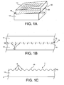
- FIGS. 1A to 1G show different steps of a first example of a process for producing an epitaxial structure according to the invention.
- the method which is the subject of the invention consists in producing the epitaxial structure by starting the deposition of the material to be epitaxially grown by columnar growth on a crystalline free surface 1 of a substrate 2 provided with a network of projections 3 on a nanometric scale such as illustrated on the figure 1D .
- These protrusions have a size of the order of 1 to a few tens of nanometers, typically 20 nanometers.
- This substrate 2 may be called a nanostructured substrate.
- the columns 4 are supported on these projections 3 and more precisely on an end zone 35 of the protrusions further called thereafter bearing zone.
- bearing zones 35 form the base of the columns 4. This deposition continues, as in the prior art, until the columns 4 join together and form a uniform continuous layer 5.
- the projections have dimensions and the network of projections a period adapted so that the material that is deposited has a desired relaxation rate of its constraints, for example the largest possible, at the time of coalescence, that is to say say at the time of the welding of the columns 4 between them.
- dimension is meant their height 36 and the size of the bearing zone 35.
- the uniform continuous layer 5 which is formed when the epitaxial deposition is continued will therefore also have some or all of the stresses relaxed. It will have a critical thickness greater than that of the layer that would have been obtained by conventional epitaxy without prior columnar growth.
- the projections 3 are obtained at the nanoscale. It may be for example substantially parallelepipedal volumes whose dimensions are of the order of a few tens of nanometers.
- This angle of rotation offset ⁇ is known as the Anglo-Saxon angle of "twist", this name will be used thereafter.
- the Figure 1A shows the contacting of the two elements 11, 12 and illustrates the "twist" angle ⁇ and the crystal lattices of the two elements 11, 12. This molecular bonding is done so that interatomic bonds are established between the two elements 11, 12 and cause, due to the angular offset, the formation of a periodic lattice of crystalline defects and / or stress fields 14 within a crystalline zone 16 located at near the bonding interface 15.
- the Figure 1B illustrates in section the structure obtained after the bonding and illustrates the network of crystalline defects and / or stress fields 14 obtained.
- the collage is done hot or cold.
- the seal will preferably be reinforced by a heat treatment to obtain this network of crystalline defects and / or stress fields 14. These crystalline defects may be dislocations.
- the crystalline zone 16 has a small thickness (a few tens of nanometers) and is located around the interface 15. This network 14 of crystalline defects and / or stress fields is at the origin of the network of projections at the nanoscale .
- the period of the lattice of crystalline defects and / or of stress fields depends on the "twist" angle ⁇ of the crystal lattices of the two elements 11, 12. It is possible to refer to the Figure 1A .
- one of the two assembled elements 11 12 is thinned, for example by rectification, by mechanical or chemical abrasion, so that the presence of the lattice 14 of crystalline defects and / or stress fields causes the level of the freed surface of protruding reliefs and recesses.
- the depressions may correspond to the crystalline defects and the projections to the crystalline material of the crystalline zone 16 or vice versa. It is on these projections 3 and more particularly on their end zone or support 35 that we will grow the columns.
- the figure 1C which shows the network of projections that has been induced.
- the structured surface obtained can be located in the first element 11, straddling the two elements 11, 12 as illustrated in FIG. figure 1C or in the second element 12 if the element 11 has been completely eliminated.
- An optional surface treatment may then be performed to further accentuate the surface relief as illustrated in the figure 1D and adjust the height 36 of the protrusions 3 and the size of their bearing zone 35.
- a chemical bath can be used to selectively attack the crystalline defects 14, without attacking their vicinity.
- a nanostructured substrate is thus obtained, that is to say provided with a network of projections 3 separated by recesses 6, these recesses and these projections being dimensioned on the nanometric scale.
- the "twist" angle between the two elements 11, 12 conditions the period of the lattice of crystalline defects and / or of the stress field as previously seen and thus also the period 38 between the projections 3.
- this period 38 With silicon as crystalline material, it is possible to modulate and control very finely this period 38, for example between a few nanometers and a few hundred nanometers with a precision of the order of a few tenths of nanometers if the adjustment of the "twist" angle takes place with a precision of the order of a hundredth of a degree.
- This accuracy can be obtained as taught in the patent application FR-A1-2 819 099 by taking the two elements 11, 12 in the same initial structure and providing this structure beforehand with one or more registration marks before the separation of the two elements. It is then sufficient to precisely control the relative angular positions of the two elements before assembling them and this is done through the registration marks. This method will be described later in figures 2 .
- This period 38 is one of the elements which makes it possible to control the moment when the columns will meet according to the thickness of the epitaxial material. It depends on the angle of "twist".
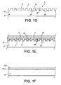
- the element which is not thinned, in the example element 12 could be formed of a stack with a film 12.1 of crystalline material covering a stop layer etching 12.2 as shown in FIG. figure 1F .
- the assembly of this element with the other can be done as described above.
- the barrier layer 12.2 may be made for example of silicon oxide, silicon nitride or amorphous silicon.
- the film 12.1 may be chosen from one of the materials mentioned below as a crystalline host material, for example made of silicon.
- the advantage of using an element 12 as illustrated in FIG. figure 1F is that during the treatment, we will locally expose the barrier layer 12.2, at the level of the recesses 6 and that thus will obtain two different materials on the surface, advantageously only one will allow the epitaxial growth.
- a second advantage is that it can independently control the height and the lateral dimensions of the projections.
- the stop layer 12.2 may be only partially attacked or not attacked.
- the attack may be a dry or wet attack, chemical, ionic, electrochemical, photochemical, thermal, under reducing or oxidizing atmosphere.
- the attack can for example have a very fast speed low in the stop layer 12.2 compared to that which exists in the crystalline material to adjust the lateral dimensions of the projections 7. It can be referred to the figure 1G .
- the barrier layer may be etched selectively vis-à-vis the material of the film 12.1 as well as the underlying layer.
- the epitaxial growth is in columnar form on the bearing zone 35 of the protrusions 3, but of course also in the depressions. It is sought by adjusting the dimensions of the projections so that the hollows are not completely filled with material. With projections 3 sufficiently high and close, for example with a height 36 of the order of 10 nanometers and a spacing 37 of the order of 3 nanometers, the columnar growth is sufficiently decoupled from the growth in the recesses 6 to allow the relaxation of the material forming the columns 4 and the formation of the uniform continuous layer whose stresses are relaxed.
- a continuous layer 5 of thickness and crystalline quality required can be obtained.
- the critical thickness 39 for this layer 5 is always greater than that which would have been obtained with a host substrate that would not be structured. If we exceed this critical thickness 39, the defect rate in the layer will be lower than that which would have been obtained for a layer of the same thickness without structuring the host substrate.
- the crystalline host material may be chosen from silicon Si, germanium Ge and gallium arsenide GaAs. , silicon carbide SiC, indium phosphide InP, sapphire, diamond, zirconia, magnesium oxide MgO, these materials being taken alone or in combination.
- the epitaxially deposited material may be chosen from silicon Si, germanium Ge, gallium nitride GaN, diamond, silicon carbide SiC, indium phosphide InP, gallium arsenide GaAs, arsenide d indium InAs, silicon-germanium Si x Ge 1-x , III-V compounds for example of InGaAs type or compounds II-VI for example of CdTe type, these materials being taken alone or in combination.
- the material of the epitaxial layer in its continuous part is in general different from that of the receiving substrate 2.
- the variation may or may not be linear.
- the epitaxial growth can be continued by germanium. AT equivalent critical thickness for the germanium layer, it will require a much smaller thickness for the epitaxial layer of Si x Ge 1-x with variable x on the bearing zones 35, than if the epitaxy of Si x Ge 1-x (with x variable) was done on a substrate that was not structured.
- An advantage of the method according to the invention over the prior art is that there is no longer need for a lithography step or mask in which it was difficult to engrave openings with a density and dimensions such as that these openings lead to an epitaxial layer whose stresses are well relaxed.
- the method of the invention since it is possible to obtain a greater density of protrusions than the density of openings etched in the mask, and this with a controlled period very precisely and since it is possible to obtain projections having a zone of support that is smaller than that of the openings of the mask, it will be easier to obtain a better relaxation of the stresses of the epitaxial layer.
- the epitaxial layer 5 formed may have constraints as minimized as possible and therefore a relaxation rate of its constraints as large as possible.
- this layer can be done without plastic relaxation and thus avoiding the formation of defects that appear traditionally because of this plastic relaxation. Nevertheless, it will be possible to choose if it is desired to exceed the critical thickness: a layer having defects will then be obtained but in a smaller quantity than a layer that would have been obtained without the invention. It is possible that the The material of the epitaxial layer has a very different mesh parameter, for example different from several percent, of the mesh parameter of the substrate material 12 having the network of projections.
- Another advantage of the method of the invention is that the formation of projections is collectively with very small dimensions, very accurately and with great regularity, regardless of the size of the assembled elements. This process applies with the same constraints both to substrates of 100 millimeters in diameter and to larger substrates, for example 150, 200 or 300 millimeters in diameter. These dimensions are standard industrial sizes of silicon substrates. With the method of the prior art, mask etching used lithographic techniques which are longer and more expensive with large substrates than with smaller ones and which are not always available for small substrates. for example less than 50 millimeters.
- one of the elements is included in a composite substrate formed of a support, a stop layer at the thinning of the support and at least the crystalline layer forming the element to be assembled.
- It may be for example a semiconductor on insulator substrate, known under the name SOI.
- An SOI substrate may comprise two layers of semiconductor material located on either side of an insulating layer. One of the layers of semiconductor material is thinner than the other. The thicker layer corresponds to the support of the composite substrate, the layer of insulation to the stop layer to the thinning of the support, the layer less thick to the element to be assembled. It is by the thinnest layer that the semiconductor on insulator substrate will be assembled to the other element.
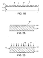
- a base substrate 100 of crystalline semiconductor material for example silicon, having a free face 101 oriented in the ⁇ 001> direction.
- This substrate may have a diameter of 100 millimeters, but a smaller or larger substrate of 150, 200 or even 300 millimeters in diameter could be used.
- the choice of this orientation ⁇ 001> makes it possible to obtain a network of projections having a symmetry of order of 4. It is of course possible to use a base substrate whose surface would have another crystalline orientation, for example for example, the crystal orientation ⁇ 111> which would give the network of projections a symmetry of order 3.
- This substrate 100 will be treated so as to be able to take two parts having crystalline surfaces which will be glued to each other thereafter.
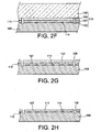
- This oxide layer 102 may have a thickness of about 400 nanometers. This step is illustrated on the Figure 2A .
- the oxide layer 102 will subsequently serve as a stop layer for thinning.
- the base substrate 100 will then be weakened by means of implanted ions, for example hydrogen ions or any other gaseous species, capable of generating a buried embrittlement zone and capable of subsequently inducing a fracture at this zone. fragilization.
- This weakening zone 104 will take the form of a plane located in the silicon of the base substrate 100, under the oxide layer 102 at a distance of the order of the implantation depth.
- the implantation is made from the free surface 101 of the oxide layer 102.
- the implantation energy may be, for example, for a silicon substrate, about 76 keV and the hydrogen ion dose is about 6.10. 16 atoms / cm 2 . Under these conditions, for an oxide layer 102 of 400 nanometers, the embrittlement zone 104 is about 760 nanometers from the free surface of the oxide layer 102. Reference is made to FIG. Figure 2B .
- One or more registration marks 105 are then produced, for example by photolithography and chemical, ionic or other etching in the oxide layer 102 and in the underlying semiconductor of the base substrate 100, these locating marks 105 encroaching in the base substrate 100 beyond the embrittlement zone 104 with respect to the oxide layer 102. Other methods of etching these registration marks could be used, for example by means of a laser .
- the registration marks 105 could pass completely through the base substrate 100. Reference can be made to the Figure 2C which illustrates these registration marks 105.
- These registration marks 105 can be configured as explained in the patent application. FR-A-2,819,099 and take the form of graduated scales such as rapporteurs. The graduations can indicate for example the degrees, the tenths of degrees, the hundredths of degrees or the thousandths of degrees. When there are two registration marks, they can be diametrically opposed on the base substrate 100.
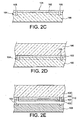
- auxiliary substrate 106 for example silicon. This assembly is done by the face carrying the oxide layer 102.
- the assembly method can be a hydrophilic molecular bonding.
- a fracture is then caused along the plane of the weakened zone 104, for example by a heat treatment, for example at 500 ° C. for one hour.
- This heat treatment also has the advantage to strengthen molecular membership.
- one of the elements 110 is a semiconductor-on-insulator substrate and in this case silicon-on-insulator, it is formed of the stack of the auxiliary substrate 106, the oxide layer 102 and the a crystalline silicon thin film 107 taken from the base substrate 100 by virtue of the fracture.
- the other element 108 corresponds to what remains of the base substrate 100.
- the two elements 108, 110 are both provided with registration marks 105 and have a crystalline portion 107, 108 which comes from the base substrate 100.
- the element 110 which is in the example is of the SOI substrate type, can be subjected to an annealing, oxidation and polishing treatment on the side of the thin film 107 which has the registration marks 105 without of course making disappear the marking marks 105. It is arranged that at the end of treatment, the thin silicon film 107 retains a thickness for example of the order of 100 nanometers.
- the other element 108 which, in the example, is solid can be subjected to a polishing of its face bearing the registration marks 105 so as to obtain a polished surface compatible with the subsequent bonding, without, of course, removing the marks of 105.
- the element 110 formed by the semiconductor-on-insulator substrate will be thinned. It is of course possible, alternatively, especially when the starting substrate is composite as described in figures 4 to thin the substrate 200 from the support 201 to the stop layer 202 as shown in FIG. figure 4D .
- the thinning of the element 110 consists in keeping all or part of the thin film 107 taken from the base substrate 100 at the 2D figure .
- the auxiliary substrate 106 which formed the thickest silicon part of the SOI substrate 110, will initially be eliminated. This elimination may be carried out, for example, by a mechanical method known to the man of the invention. art then by a chemical method using for example TMAH (trimethylammonium hydroxide).
- TMAH trimethylammonium hydroxide
- the oxide layer 102 is then removed by etching, for example by means of an aqueous solution of hydrofluoric acid HF.
- the hydrofluoric acid concentration can be 10%.
- the thin film 107 is then thinned, its thickness may, for example, be reduced to less than 20 nanometers.
- This thinning may consist of chemical etching and / or thermal oxidation followed by etching, the etching being possible for example by means of an aqueous solution of hydrofluoric acid.
- the sequence of the thermal oxidation followed by the chemical attack corresponds to a sacrificial treatment.
- the free surface 111 of the thinned film 107 does not reveal the presence of the lattice of crystalline defects and / or stress fields 114.
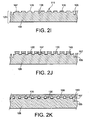
- the structure represented in FIG. figure 2H The next step, illustrated in figure 2I is to treat the thinned film 107 so that its free face 111 reveals the presence of the lattice of crystalline defects and / or stress fields 114 around the bonding interface 115.
- This treatment can be a chemical attack that preferentially attacks the areas of stress.
- a surface is obtained with a network of projections 130 at the nanoscale.
- This chemical attack can be carried out using aqueous chemical solutions based on hydrofluoric acid and chromium trioxide CrO 3 / HF; hydrofluoric acid and nitric acid HNO 3 / HF; of dichromate ions and hydrofluoric acid Cr 2 O 7-- / HF. It is possible to add to these solutions acetic acid and / or an alcohol such as ethanol or propanol and / or ammonia.
- the revelation step can be completed by other surface treatment steps such as other chemical etchings, ion etches (RIE). , oxidation and deoxidation, electrochemical attacks, photochemical, deposits of material etc ........ It may for example deposit germanium, typically the equivalent of a film of 1 nanometer.
- the deposit will be mainly on the support zones 135 which are silicon in our example. It will then be possible to increase the height of the projections 130 by selectively etching the silicon with respect to the germanium.
- the germanium thin film located on the bearing zones 135 may optionally be removed before the columnar epitaxy step.
- protrusions 130 of about 10 nanometers in height, two adjacent protrusions 130 being spaced apart by about 4 nanometers and the period of the grating being about 20 nanometers. It is specified that the period corresponds to the interval formed by a support zone and the spacing that follows or precedes it.
- the revelation step may consist of a thermal budget contribution.
- This thermal budget can be provided in the form of at least one annealing, possibly in the presence of a particular gas or under vacuum.
- This thermal budget is intended to cause a change in the topology of the free surface 111 of the thin film 107 by revealing projections 130 and hollows which depend on the topology of the lattice of crystalline defects and / or stress fields 114 which is in the vicinity of the interface 115, that is to say which is buried with respect to the free surface 111 of the thin film 107.
- Other methods can be used to reveal the lattice of crystal defects and / or stress fields 114 such as the introduction of chemical species into the thin film 107 or into the other element 108, for example by diffusion or ion implantation.
- the introduction of chemical species can coexist with the contribution of the thermal budget, this introduction can take place before and / or after and / or during the contribution of the thermal budget.
- the introduced chemical species may be gold, copper, titanium, aluminum, or a dopant, for example boron for silicon.
- the chemical species introduced are located at the level of defects and / or zones of maximum stress. It is then possible to reveal the network of projections to use for example a selective etching step.
- the revelation can also be done by etching and / or electrochemical and / or ionic and / or photochemical and / or mechanical thinned element (thin film 107 or 108 element). In the same way this attack can coexist with the contribution of the thermal budget, it can take place before and / or after and / or during the contribution of the thermal budget.
- the attack step (s) can be carried out under various oxidizing or reducing atmospheres.
- the epitaxy may be for example a gas phase epitaxy or a molecular epitaxy (known by the acronym MBE for molecular beam epitaxy).
- MBE molecular beam epitaxy
- columns 140 are formed on the support zone 135 of the projections as illustrated in FIG. figure 2J .
- the deposit continues and the columns 140 widen, increase their diameter and eventually meet.
- the continuous layer 150 then takes shape as on the figure 2K .
- the material which is deposited on the projections 130 will relax its stress by modifying the diameter of the columns 140.
- the measurement of the mesh parameters indicates the stress relaxation rate of the deposited material.
- the geometric parameters of the columns 140 that is to say their base section, will be very precisely controlled. their spacing and from the size of the bearing zone 135 of the projections 130, their height 136 and their spacing 137.
- the continuous epitaxial layer 150 obtained may be transferred to another substrate with or without a crystallographic relationship with it.
- the other substrate that will receive the epitaxial continuous layer may be for example plastic, glass, another crystalline material, for example, semiconductor such as silicon, oxide of a material such as silica or even carbide of a semiconductor material such as silicon carbide.
- This transfer can be done by implantation of gaseous species capable of providing a buried fragile zone and then fracture at this zone, for example by thermal and / or mechanical treatment as described in the patent application.
- FR-A-2,681,472 are examples of gaseous species capable of providing a buried fragile zone and then fracture at this zone, for example by thermal and / or mechanical treatment as described in the patent application.
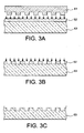
- NIL nanoimprint lithography
- This technique consists in molding the network of protrusions of the substrate 61 (called the parent substrate) by a layer, for example, of resin 62 carried by a substrate 63 as illustrated on FIG. figure 3A .
- This postponement can be done, for example, by hot embossing or ultraviolet exposure ( figure 3B ).
- the substrate 63 which is for example made of silicon, is then etched using the openwork resin layer 62 as a mask.
- the etching can be an ion etching (RIE).
- RIE ion etching
- a crystalline substrate 64 is then covered with a layer of, for example, polymeric resin 65.
- the mold cavity 63 is left in the polymer layer 65, for example, by hot embossing or ultraviolet exposure, as shown on FIG. the 3D and 3E figures .
- the crystalline substrate 64 is then etched through the imprint left in the polymer resin layer 65 as shown in FIG. figure 3F .
- a replica of the mother substrate 61 having a network of projections substantially identical to that of the parent substrate is then obtained. This technique of nanoimprint lithography is described for example in the article Replication of sub-40nm gap nanoelectrodes over an 8-in. Substrate by nanoimprint lithography Tallal J. et al, Microelectronic engineering, 2005, vol.78-79 pages 676 to 681 .
Abstract
Description
La présente invention est relative à un procédé de réalisation d'une structure épitaxiée. On rappelle que l'épitaxie est une technique de croissance de cristaux utilisée pour former, à la surface d'un substrat cristallin d'accueil des couches dont les axes cristallins sont en relation avec les axes cristallins du substrat d'accueil. On parle d'hétéroépitaxie si le matériau déposé est d'une autre espèce chimique que celle du substrat d'accueil. Des substrats ainsi revêtus ont un grand intérêt pour la fabrication de dispositifs semi-conducteurs, optiques ou optoélectroniques. L'optimisation de la croissance cristalline des couches permet d'améliorer la performance de ces dispositifs.The present invention relates to a method for producing an epitaxial structure. It is recalled that epitaxy is a crystal growth technique used to form, on the surface of a crystalline host substrate, layers whose crystalline axes are in relation to the crystalline axes of the host substrate. Heteroepitaxy is called if the deposited material is of a different chemical species than that of the host substrate. Substrates thus coated are of great interest for the manufacture of semiconductor, optical or optoelectronic devices. The optimization of the crystalline growth of the layers makes it possible to improve the performance of these devices.
La réalisation d'un dépôt par hétéroépitaxie sur un substrat engendre des dislocations de désaccord de maille (connu sous la dénomination anglo-saxonne de misfit) à partir d'une certaine épaisseur de couche déposée dite épaisseur critique. Cette épaisseur dépend de la différence des paramètres de maille entre le matériau épitaxié et celle du substrat d'accueil. On peut se référer par exemple à l'article de
De nombreuses méthodes existent pour atténuer cet inconvénient. Parmi celles-ci une méthode consiste au préalable à faire d'abord croître par épitaxie des colonnes (quelquefois appelés îlots dans la littérature) espacées les unes des autres sur le substrat d'accueil. L'avantage en est que le matériau épitaxié en poussant sous forme de colonnes peut relaxer sa contrainte sur la surface libre du substrat d'accueil. Par exemple dans le cas d'une croissance en compression d'une colonne sur un substrat, la colonne va progressivement s'évaser, son diamètre augmentant pour relaxer la contrainte au sein du matériau déposé. Inversement dans le cas d'une croissance en extension d'une colonne, celle-ci va progressivement se rétrécir, son diamètre tendant à diminuer pour relaxer sa contrainte. Simultanément à la relaxation de contrainte, il se produit une croissance latérale qui tend à augmenter en permanence le diamètre des colonnes. Ainsi, à force de s'évaser, les colonnes finissent par se rejoindre pour former une couche continue. On peut modifier les conditions de dépôt pour favoriser la croissance latérale et la coalescence, c'est-à-dire la soudure des colonnes venant en contact. Si l'espacement des colonnes est approprié, au moment où les colonnes se rejoignent, le matériau épitaxié aura relaxé tout ou partie de sa contrainte et aura ainsi retrouvé tout au partie de son paramètre de maille naturel. Le niveau de relaxation peut être quantifié par le taux de relaxation correspondant au rapport entre le niveau de contrainte de départ et celui obtenu après l'épitaxie en l'absence d'apparition de défauts. En continuant le dépôt par épitaxie, on obtient une couche de matière qui ne possède que peu voire pas de dislocations puisqu'on s'est affranchi de tout ou partie des contraintes de désaccord de paramètres de maille. L'épaisseur critique que l'on peut obtenir pour cette couche est supérieure à celle que l'on aurait obtenu par épitaxie standard ou conventionnelle sur toute la surface du substrat d'accueil.Many methods exist to mitigate this disadvantage. Among these, one method consists in first having epitaxially grown columns (sometimes called islands in the literature) spaced apart from one another on the host substrate. The advantage is that the epitaxial material growing in the form of columns can relax its stress on the free surface of the host substrate. For example, in the case of growth in compression of a column on a substrate, the column will gradually flake out, its diameter increasing to relax the stress within the deposited material. Conversely, in the case of growth in extension of a column, it will gradually shrink, its diameter tending to decrease to relax its stress. Simultaneously with stress relaxation, there is a lateral growth which tends to permanently increase the diameter of the columns. Thus, by dashing, the columns eventually meet to form a continuous layer. The deposition conditions can be modified to promote lateral growth and coalescence, i.e., welding of the contacting columns. If the spacing of the columns is appropriate, as the columns meet, the epitaxial material will have relaxed all or part of its stress and will have found all the part of its natural mesh parameter. The level of relaxation can be quantified by the rate of relaxation corresponding to the ratio between the level of stress of departure and that obtained after epitaxy in the absence of appearance of defects. By continuing the epitaxial deposition, a layer of material is obtained which possesses little or no dislocations since all or some of the mesh parameter mismatch constraints have been overcome. The critical thickness that can be obtained for this layer is greater than that obtained by standard or conventional epitaxy over the entire surface of the host substrate.
Une technique employée pour obtenir les colonnes consiste à délimiter à la surface du substrat d'accueil des germes de croissance localisés, ces germes de croissance ayant une surface appropriée qui correspond à celle de la base des colonnes. Pour cela on peut disposer sur la surface d'accueil du substrat un masque de croissance, ce masque étant doté d'ouvertures mettant à nu le substrat d'accueil. Le substrat à nu au fond des ouvertures forme les germes de croissance. En variante, il est possible comme décrit dans l'article
Les problèmes engendrés par cette méthode sont qu'elle nécessite une étape de lithographie pour graver le masque ou la couche cristalline et ainsi définir les germes de croissance. Or ces germes de croissance doivent être réalisés à l'échelle nanométrique, leur taille typique étant comprise entre un et quelques dizaines de nanomètres, et doivent être répartis de manière très régulière à la surface du substrat d'accueil, la distance entre ces germes étant de l'ordre de la dizaine à quelques centaines de nanomètres. Actuellement, il n'est pas connu de méthode satisfaisante pour réaliser de manière collective et ordonnée de tels germes de croissance à l'échelle d'un substrat de diamètre pouvant aller jusqu'à 300 millimètres et plus.The problems caused by this method are that it requires a lithography step to engrave the mask or the crystalline layer and thus define the growth seeds. However, these growth seeds must be made at the nanoscale, their typical size being between one and a few tens of nanometers, and must be distributed very evenly over the surface of the host substrate, the distance between these seeds being from the order of ten to a few hundred nanometers. Currently, it is not known satisfactory method to achieve collectively and ordinarily such growth seeds on a scale of a substrate diameter of up to 300 millimeters and more.
La présente invention vise à proposer un procédé de réalisation d'une structure épitaxiée par croissance de colonnes à l'échelle nanométrique sans à avoir recours à une étape de lithographie à l'échelle nanométrique. Ce substrat est obtenu de manière économique et peut posséder une grande surface. La position et la géométrie des colonnes sont obtenues avec grande précision.The present invention aims at providing a method for producing a structure grown by nanoscale growth of columns without having to resort to a nanoscale lithography step. This substrate is economically obtained and can have a large surface area. The position and geometry of the columns are obtained with great precision.
Plus précisément, la présente invention est un procédé de réalisation d'une structure épitaxiée consistant à déposer un matériau par croissance épitaxiale colonnaire sur une face cristalline d'un substrat, à poursuivre le dépôt jusqu'à ce que les colonnes se rejoignent et conduisent à une couche continue. Il consiste à pourvoir la face du substrat d'un réseau périodique de saillies à l'échelle nanométrique, chaque saillie présentant une zone d'appui pour une colonne, et étant obtenue directement ou indirectement à partir d'un réseau de défauts cristallins et/ou de champs de contraintes créé au sein d'une zone cristalline située au voisinage d'une interface de collage entre deux éléments comprenant du matériau cristallin et ayant des réseaux cristallins décalés en rotation et/ou en flexion et/ou présentant un désaccord de paramètres de maille à l'interface, aptes à conditionner la période du réseau de saillies, la période du réseau, la hauteur des saillies et la taille de leur zone d'appui étant ajustées de manière que la couche continue ait une épaisseur critique supérieure à celle obtenue lors d'une épitaxie réalisée en l'absence des saillies.More specifically, the present invention is a process for producing an epitaxial structure consisting of depositing a material by columnar epitaxial growth on a crystalline face of a substrate, to continue the deposition until the columns meet and lead to a continuous layer. It consists in providing the face of the substrate with a periodic network of nanoscale protrusions, each protrusion having a bearing zone for a column, and being obtained directly or indirectly from a lattice of crystalline defects and / or constraint fields created within a crystalline zone located in the vicinity of a bonding interface between two elements comprising crystalline material and having crystal lattices offset in rotation and / or in flexion and / or having a disagreement of parameters mesh at the interface, able to condition the period of the network of projections, the period of the network, the height of the projections and the size of their support zone being adjusted so that the continuous layer has a critical thickness greater than that obtained during an epitaxy performed in the absence of projections.
Il est préférable que la période du réseau, la hauteur des saillies et la taille de leur zone d'appui soient ajustées de manière que le matériau déposé par épitaxie ait retrouvé son paramètre de maille naturel au moment où les colonnes se rejoignent.It is preferable that the period of the grating, the height of the protrusions and the size of their support zone are adjusted so that the epitaxially deposited material has found its natural mesh parameter at the moment when the columns meet.
Le substrat dont la face est dotée du réseau de saillies peut être réalisé à partir des deux éléments collés, en amincissant l'un des éléments jusqu'à faire apparaître un relief de surface correspondant réseau de défauts cristallins et/ou de champs de contraintes, ce relief formant alors le réseau de saillies, ce réseau de saillies étant supporté par l'autre élément.The substrate, the face of which is provided with the network of projections, can be made from the two bonded elements, by thinning one of the elements until a surface relief corresponding to the network of crystalline defects and / or stress fields appears, this relief then forming the network of projections, this network of projections being supported by the other element.
L'amincissement peut comprendre au moins une étape choisie parmi une abrasion mécanique, une abrasion chimique, une rectification, un traitement sacrificiel.Thinning may comprise at least one step selected from mechanical abrasion, chemical abrasion, rectification, sacrificial treatment.
Le procédé peut comprendre en outre une étape de traitement du réseau de saillies de manière à ajuster la hauteur et/ou la taille de la zone d'appui des saillies et/ou à modifier le paramètre de maille du matériau constitutif des saillies.The method may further comprise a step of processing the array of projections so as to adjust the height and / or the size of the bearing area of the projections and / or to modify the mesh parameter of the material constituting the projections.
L'étape de traitement du réseau de saillies peut comprendre une étape d'implantation.The step of processing the network of projections may comprise an implantation step.
L'étape d'amincissement et/ou de traitement du réseau de saillies peut comprendre au moins une étape d'attaque chimique et/ou d'attaque électrochimique et/ou d'attaque mécanique et/ou d'attaque ionique et/ou d'attaque photochimique et/ou un dépôt.The step of thinning and / or treatment of the network of projections may comprise at least one etching step and / or electrochemical etching and / or mechanical etching and / or ion etching and / or photochemical attack and / or depot.
L'étape d'amincissement et/ou de traitement du réseau de saillies peut comprendre l'apport d'un budget thermique, sous des atmosphères diverses, oxydantes ou réductrices.The step of thinning and / or treatment of the network of projections may include the provision of a thermal budget, in various atmospheres, oxidizing or reducing.
Pour former les éléments, on peut prélever dans une même structure cristalline au moins deux parties, ces deux parties contribuant à la formation de l'interface de collage.To form the elements, at least two crystalline structures can be parts, these two parts contributing to the formation of the bonding interface.
Lors du collage les deux parties ont de préférence leurs réseaux cristallins décalés en rotation et/ou en flexion d'un angle prédéterminé.During gluing, the two parts preferably have their crystal lattices offset in rotation and / or in flexion by a predetermined angle.
La structure cristalline comporte de préférence des marques de repérage qui sont reportées dans les deux parties lors du prélèvement, ces marques de repérage étant utilisées pour ajuster l'angle de décalage.The crystalline structure preferably has registration marks which are reported in both parts during sampling, these registration marks being used to adjust the offset angle.
Au moins un des éléments est un substrat composite formé d'un empilement d'un support, d'une couche d'arrêt à l'amincissement du support et d'au moins une couche cristalline.At least one of the elements is a composite substrate formed of a stack of a support, a stop layer at the thinning of the support and at least one crystalline layer.
L'étape d'amincissement concerne de préférence le substrat composite.The thinning step preferably relates to the composite substrate.
Le substrat composite peut être un substrat SOI.The composite substrate may be an SOI substrate.
La partie prélevée dans le substrat composite comprend au moins la couche cristalline.The portion taken from the composite substrate comprises at least the crystalline layer.
Le collage peut se faire par adhésion moléculaire.The bonding can be done by molecular adhesion.
Il est possible de faire varier la composition du matériau déposé pendant le dépôt par épitaxie.It is possible to vary the composition of the deposited material during the epitaxial deposition.
En variante, le substrat dont la face est pourvue du réseau de saillies peut être réalisé par duplication d'un substrat mère dont une face comporte un réseau de saillies à l'échelle nanométrique, le substrat mère étant obtenu à partir des deux éléments collés et par au moins une étape d'amincissement de l'un des éléments conduisant directement ou indirectement à une révélation du réseau de défauts cristallins et/ou de champs de contraintes, ce réseau de défauts cristallins et/ou de champs de contraintes formant le réseau de saillies.As a variant, the substrate whose face is provided with the network of projections may be made by duplication of a mother substrate whose one face comprises a network of projections at the nanometric scale, the mother substrate being obtained from the two bonded elements and by at least one step of thinning one of the elements leading directly or indirectly to a revelation of the network of crystalline defects and / or stress fields, this network of crystalline defects and / or stress fields forming the network of projections.
La duplication peut se faire par nanoimpression à partir d'un moule complémentaire du substrat mère.Duplication can be done by nanoimprinting from a complementary mold of the parent substrate.
Quant au moule, il peut être obtenu par nanoimpression à partir du substrat mère.As for the mold, it can be obtained by nanoimpression from the mother substrate.
La présente invention concerne également une structure épitaxiée comportant des colonnes (4) de matériau épitaxié s'évasant de manière à se rejoindre et à former une couche continue. Chaque colonne repose sur une zone d'appui d'une saillie d'un réseau périodique de saillies à l'échelle nanométrique dont est dotée une face d'un substrat, ces saillies provenant directement ou indirectement d'un réseau de défauts cristallins et/ou de champs de contraintes, les saillies du réseau ayant une période, une hauteur et une taille de zone d'appui ajustées de manière à ce que la couche continue ait une épaisseur critique supérieure à celle obtenue lors d'une épitaxie réalisée en l'absence des saillies.The present invention also relates to an epitaxial structure comprising columns (4) of epitaxial material flaring so as to meet and form a continuous layer. Each column rests on a support zone of a protrusion of a periodic network of protrusions at the nanoscale which is provided with a face of a substrate, these protrusions coming directly or indirectly from a lattice of crystalline defects and / or stress fields, the protrusions of the grating having a period, a height and a size of support zone adjusted so that the continuous layer has a critical thickness greater than that obtained during an epitaxy performed in the absence of projections.
La présente invention sera mieux comprise à la lecture de la description d'exemples de réalisation donnés, à titre purement indicatif et nullement limitatif, en faisant référence aux dessins annexés sur lesquels :
- les
figures 1A à 1G montrent des étapes de réalisation d'une structure épitaxiée par un premier exemple du procédé selon l'invention ; - les
figures 2A à 2K montrent des étapes de réalisation d'une structure épitaxiée par un autre exemple du procédé selon l'invention ; - les
figures 3A à 3F montrent des étapes de réalisation d'une structure épitaxiée par encore un autre exemple du procédé selon l'invention ; - les
figures 4A à 4D montrent l'utilisation d'un substrat composite dans l'exemple desfigures 2 au lieu d'un substrat massif.
- the
Figures 1A to 1G show steps of producing an epitaxial structure by a first example of the method according to the invention; - the
Figures 2A to 2K show steps for producing an epitaxial structure by another example of the method according to the invention; - the
Figures 3A to 3F show steps of producing an epitaxial structure by yet another example of the method according to the invention; - the
Figures 4A to 4D show the use of a composite substrate in the example offigures 2 instead of a massive substrate.
Des parties identiques, similaires ou équivalentes des différentes figures portent les mêmes références numériques de façon à faciliter le passage d'une figure à l'autre.Identical, similar or equivalent parts of the different figures bear the same numerical references so as to facilitate the passage from one figure to another.
Les différentes parties représentées sur les figures ne le sont pas nécessairement selon une échelle uniforme, pour rendre les figures plus lisibles.The different parts shown in the figures are not necessarily in a uniform scale, to make the figures more readable.
On peut se référer aux
On va voir maintenant comment sont obtenues les saillies 3 à l'échelle nanométrique. Il peut s'agir par exemple de volumes sensiblement parallélépipédiques dont les dimensions sont de l'ordre du ou de quelques dizaines de nanomètres.We will now see how the
Plusieurs manières simples d'obtenir ce réseau de saillies 3 à l'échelle nanométrique sont expliquées dans la demande de brevet
Cet angle de décalage en rotation θ, est connu sous la dénomination anglo-saxonne d'angle de « twist », cette dénomination sera employée par la suite.This angle of rotation offset θ is known as the Anglo-Saxon angle of "twist", this name will be used thereafter.
Dans le cas d'un collage entre deux plaquettes de silicium de direction cristalline <001> par exemple, l'introduction d'un angle de «twist » θ donné produit un réseau carré de dislocations. L'introduction d'un angle de « tilt » produirait quant à elle un réseau unidimensionnel de dislocations.In the case of bonding between two <001> crystalline silicon wafers for example, the introduction of a given "twist" angle θ produces a square array of dislocations. The introduction of a tilt angle would produce a one-dimensional network of dislocations.
La
Le collage se fait à chaud ou bien à froid. Le scellement sera, de préférence, renforcé par un traitement thermique pour obtenir ce réseau de défauts cristallins et/ou de champs de contraintes 14. Ces défauts cristallins peuvent être des dislocations. La zone cristalline 16 a une faible épaisseur (quelques dizaines de nanomètres) et est localisée autour l'interface 15. Ce réseau 14 de défauts cristallins et/ou de champs de contraintes est à l'origine du réseau de saillies à l'échelle nanométrique.The collage is done hot or cold. The seal will preferably be reinforced by a heat treatment to obtain this network of crystalline defects and / or stress fields 14. These crystalline defects may be dislocations. The
La période du réseau de défauts cristallins et/ou de champs de contraintes dépend de l'angle de «twist» θ des réseaux cristallins des deux éléments 11, 12. On peut se référer à la
Subséquemment, on amincit l'un des deux éléments assemblés 11 12, par exemple par rectification, par abrasion mécanique ou chimique, de sorte que la présence du réseau 14 de défauts cristallins et/ou de champs de contraintes induise au niveau de la surface libérée des reliefs en saillie et en creux. Les creux peuvent correspondre aux défauts cristallins et les saillies au matériau cristallin de la zone cristalline 16 ou réciproquement. C'est sur ces saillies 3 et plus particulièrement sur leur zone d'extrémité ou d'appui 35 que l'on va faire croître les colonnes. On peut se référer à la
Un traitement de surface optionnel peut être réalisé ensuite pour accentuer encore plus le relief en surface comme illustré sur la
Cette période 38 est un des éléments qui permet de contrôler le moment où les colonnes vont se rejoindre en fonction de l'épaisseur de matière épitaxiée. Elle dépend de l'angle de « twist ».This
L'opération de révélation du réseau de saillies 3 et celle éventuelle de traitement pour accentuer le relief des saillies 3 permettent quant à elles de faire varier la hauteur 36 et/ou la taille de la zone d'appui 35 des saillies 3. La période 38 du réseau étant fixée par l'angle de « twist », l'espacement 37 entre les saillies évolue en même temps que la taille de la zone d'appui 35.The operation of revealing the network of
En variante, l'élément qui n'est pas aminci, dans l'exemple l'élément 12, pourrait être formé d'un empilement avec un film 12.1 en matériau cristallin recouvrant une couche d'arrêt à la gravure 12.2 comme illustré à la
L'avantage d'utiliser un élément 12 tel qu'illustré à la
La couche d'arrêt 12.2 peut n'être que partiellement attaquée ou ne pas être attaquée. L'attaque peut être une attaque sèche ou humide, chimique, ionique, électrochimique, photochimique, thermique, sous atmosphère réductrice ou oxydante. L'attaque peut par exemple avoir une vitesse très faible dans la couche d'arrêt 12.2 par rapport à celle qui existe dans le matériau cristallin pour ajuster les dimensions latérales des saillies 7. On peut se référer à la
Pour accroître la hauteur des saillies, la couche d'arrêt pourra être gravée sélectivement vis-à-vis du matériau du film 12.1 de même que la couche sous-jacente.To increase the height of the projections, the barrier layer may be etched selectively vis-à-vis the material of the film 12.1 as well as the underlying layer.
La croissance épitaxiale se fait sous forme colonnaire sur la zone d'appui 35 des saillies 3 mais bien sûr également dans les creux. On cherche en ajustant les dimensions des saillies à ce que les creux ne soient pas totalement emplis de matériau. Avec des saillies 3 suffisamment hautes et proches, par exemple avec une hauteur 36 de l'ordre de 10 nanomètres et un espacement 37 de l'ordre de 3 nanomètres, la croissance colonnaire est suffisamment découplée de la croissance dans les creux 6 pour permettre la relaxation du matériau formant les colonnes 4 et la formation de la couche continue uniforme dont les contraintes sont relaxées.The epitaxial growth is in columnar form on the
En jouant sur les trois paramètres qui sont la hauteur 36 des saillies, la taille de leur zone d'appui 35 et leur période 38, il est possible de faire croître des matériaux différents, en paramètre de maille, sur des substrats 2 d'un matériau donné dotés d'un réseau de saillies adapté.By playing on the three parameters which are the
Après épitaxie, on peut obtenir une couche continue 5 d'épaisseur et de qualité cristalline requise. L'épaisseur critique 39 pour cette couche 5 est toujours supérieure à celle que l'on aurait obtenu avec un substrat d'accueil qui ne serait pas structuré. Si on dépasse cette épaisseur critique 39, le taux de défauts dans la couche sera inférieur à celui qui aurait été obtenu pour une couche de même épaisseur sans structurer le substrat d'accueil.After epitaxy, a
A titre d'exemple le matériau cristallin d'accueil, c'est-à-dire celui des saillies ou bien souvent celui du substrat 2 doté des saillies peut être choisi parmi le silicium Si, le germanium Ge, l'arséniure de gallium GaAs, le carbure de silicium SiC, le phosphure d'indium InP, le saphir, le diamant, la zircone, l'oxyde de magnésium MgO, ces matériaux étant pris seuls ou en combinaison. Le matériau déposé par épitaxie peut être choisi parmi le silicium Si, le germanium Ge, le nitrure de gallium GaN , le diamant, le carbure de silicium SiC, le phosphure d'indium InP, l'arséniure de gallium GaAs, l'arséniure d'indium InAs, le silicium-germanium SixGe1-x, les composés III-V par exemple de type InGaAs ou les composés II-VI par exemple de type CdTe, ces matériaux étant pris seuls ou en combinaison. Le matériau de la couche épitaxiée dans sa partie continue est en général différent de celui du substrat d'accueil 2.By way of example, the crystalline host material, that is to say that of the projections or often that of the
Il peut être intéressant de faire varier la composition du matériau déposé pendant l'épitaxie. Ainsi sur un substrat structuré de silicium, on pourra faire croître du SixGe1-x avec x variant entre une première valeur α telle que 0 < α < 1 et une seconde valeur β telle que 0 ≤ β < 1 (avantageusement β=0). La variation pourra ou non être linéaire. On pourra poursuivre la croissance épitaxiale par du germanium. A épaisseur critique équivalente pour la couche de germanium, il faudra une épaisseur beaucoup plus petite pour la couche épitaxiée de SixGe1-x avec x variable sur les zones d'appui 35, que si l'épitaxie de SixGe1-x (avec x variable) se faisait sur un substrat qui n'était pas structuré.It may be interesting to vary the composition of the deposited material during epitaxy. Thus, on a structured silicon substrate, Si x Ge 1-x can be grown with x varying between a first value α such that 0 <α <1 and a second value β such that 0 ≤ β <1 (advantageously β = 0). The variation may or may not be linear. The epitaxial growth can be continued by germanium. AT equivalent critical thickness for the germanium layer, it will require a much smaller thickness for the epitaxial layer of Si x Ge 1-x with variable x on the
Un avantage du procédé selon l'invention par rapport à l'art antérieur est que l'on n'a plus besoin d'étape de lithographie ni de masque dans lequel on avait du mal à graver des ouvertures avec une densité et des dimensions telles que ces ouvertures conduisent à une couche épitaxiée dont les contraintes sont bien relaxées. Avec le procédé de l'invention, puisqu'on peut obtenir une densité de saillies plus importante que la densité d'ouvertures gravées dans le masque, et ce avec une période contrôlée très précisément et puisque on peut obtenir des saillies ayant une zone d'appui qui est plus petite que celle des ouvertures du masque, on va obtenir plus facilement une meilleure relaxation des contraintes de la couche épitaxiée. La couche épitaxiée formée 5 pourra avoir des contraintes aussi minimisées que possible et donc un taux de relaxation de ses contraintes le plus grand possible. La croissance de cette couche pourra se faire sans relaxation plastique et donc en évitant la formation de défauts qui apparaissent traditionnellement à cause de cette relaxation plastique. On pourra néanmoins choisir si on le souhaite de dépasser l'épaisseur critique : on obtiendra alors une couche présentant des défauts mais en quantité moindre qu'une couche que l'on aurait obtenu sans l'invention. Il est possible que le matériau de la couche épitaxiée ait un paramètre de maille très différent, par exemple différent de plusieurs pourcents, du paramètre de maille du matériau du substrat 12 d'accueil doté du réseau de saillies.An advantage of the method according to the invention over the prior art is that there is no longer need for a lithography step or mask in which it was difficult to engrave openings with a density and dimensions such as that these openings lead to an epitaxial layer whose stresses are well relaxed. With the method of the invention, since it is possible to obtain a greater density of protrusions than the density of openings etched in the mask, and this with a controlled period very precisely and since it is possible to obtain projections having a zone of support that is smaller than that of the openings of the mask, it will be easier to obtain a better relaxation of the stresses of the epitaxial layer. The
Un autre avantage du procédé de l'invention est que la formation des saillies se fait de manière collective avec des dimensions très petites, de manière très précise et avec une grande régularité, quelle que soit la taille des éléments assemblés. Ce procédé s'applique avec les mêmes contraintes aussi bien aux substrats de 100 millimètres de diamètre qu'aux substrats plus grands par exemple de 150, 200 ou 300 millimètres de diamètre. Ces dimensions sont des dimensions standard industrielles des substrats de silicium. Avec le procédé de l'art antérieur, la gravure du masque avait recours à des techniques de lithographie qui sont plus longues et plus coûteuses avec de grands substrats qu'avec de plus petits et qui ne sont pas toujours disponibles pour des substrats de petites dimensions par exemple inférieures à 50 millimètres.Another advantage of the method of the invention is that the formation of projections is collectively with very small dimensions, very accurately and with great regularity, regardless of the size of the assembled elements. This process applies with the same constraints both to substrates of 100 millimeters in diameter and to larger substrates, for example 150, 200 or 300 millimeters in diameter. These dimensions are standard industrial sizes of silicon substrates. With the method of the prior art, mask etching used lithographic techniques which are longer and more expensive with large substrates than with smaller ones and which are not always available for small substrates. for example less than 50 millimeters.
On va maintenant, en se référant aux
Dans cet exemple, on part d'un substrat de base 100 de matériau semi-conducteur cristallin, par exemple du silicium, présentant une face libre 101 orientée dans la direction <001>. Ce substrat peut avoir un diamètre 100 millimètres, mais on pourrait utiliser un substrat plus petit ou plus grand de 150, 200 ou même 300 millimètres de diamètre. Le choix de cette orientation <001> permet d'obtenir un réseau de saillies ayant une symétrie d'ordre de 4. Il est bien sûr possible d'utiliser un substrat de base dont la surface aurait une autre orientation cristalline, par exemple, l'orientation cristalline <111> qui conférerait au réseau de saillies une symétrie d'ordre 3.In this example, we start from a
On va traiter ce substrat 100 de manière à pouvoir en prélever deux parties ayant des surfaces cristallines qui seront collées l'une à l'autre par la suite. On peut commencer par former une couche d'oxyde 102 en oxydant thermiquement la face libre 101. Cette couche d'oxyde 102 peut avoir une épaisseur d'environ 400 nanomètres. Cette étape est illustrée sur la
On va ensuite fragiliser le substrat de base 100 au moyen d'ions implantés par exemple des ions d'hydrogène ou de toute autre espèce gazeuse, apte à générer une zone de fragilisation enterrée et capable d'induire ultérieurement une fracture au niveau de cette zone de fragilisation. Cette zone de fragilisation 104 va prendre la forme d'un plan situé dans le silicium du substrat 100 de base, sous la couche d'oxyde 102 à une distance de l'ordre de la profondeur d'implantation. L'implantation se fait depuis la surface libre 101 de la couche d'oxyde 102. L'énergie d'implantation peut être par exemple, pour un substrat de silicium, d'environ 76 keV et la dose d'ions hydrogène valoir environ 6.1016 atomes/cm2. Dans ces conditions, pour une couche d'oxyde 102 de 400 nanomètres, la zone de fragilisation 104 se trouve à environ 760 nanomètres de la surface libre de la couche d'oxyde 102. On se réfère à la
On réalise ensuite une ou plusieurs marques de repérage 105, par exemple par photolithograhie et gravure chimique, ionique ou autre dans la couche d'oxyde 102 et dans le semi-conducteur sous-jacent du substrat de base 100, ces marques de repérage 105 empiétant dans le substrat de base 100 au-delà de la zone de fragilisation 104 par rapport à la couche d'oxyde 102. D'autres méthodes de gravure de ces marques de repérage pourraient être utilisées, par exemple à l'aide d'un laser. Les marques de repérage 105 pourraient traverser totalement le substrat de base 100. On peut se référer à la
On assemble ensuite, à la
On provoque ensuite une fracture le long du plan de la zone fragilisée 104, par exemple par un traitement thermique, par exemple à 500°C pendant une heure. Ce traitement thermique a aussi comme avantage de renforcer l'adhésion moléculaire. On est alors en présence de deux éléments 110, 108 comme illustré sur la
L'élément 110, qui est dans l'exemple est de type substrat SOI, peut être soumis à un traitement de recuit, d'oxydation et de polissage du côté du film mince 107 qui comporte les marques de repérage 105 sans bien sûr faire disparaître les marques de repérage 105. On s'arrange pour qu'en fin de traitement, le film mince de silicium 107 conserve une épaisseur par exemple de l'ordre de 100 nanomètres. L'autre élément 108 qui, dans l'exemple, est massif peut être soumis à un polissage de sa face portant les marques de repérage 105 afin d'obtenir une surface polie compatible avec le collage ultérieur, sans bien sûr faire disparaître les marques de repérage 105. Ce sont ces deux parties cristallines 108, 107 que l'on va coller l'une à l'autre, au niveau d'une interface de collage, par adhésion moléculaire, par exemple, hydrophobe en introduisant un angle de « twist » déterminé de façon très précise, grâce à la présence des marques de repérage 105 sur les deux parties cristallines 107, 108. La valeur de l'angle de « twist » peut être, par exemple de 0,44° ou de 1,1°. Ces valeurs vont créer un réseau de défauts cristallins et/ou de champs de contraintes de symétrie 4 et ayant une période respectivement de 50 et 20 nanomètres. On peut se référer à la
En variante, il serait possible de partir non pas d'un substrat de base massif mais d'un substrat de base composite 200 comme défini précédemment avec un support 201, une couche d'arrêt 202 à l'amincissement du support et au moins une couche cristalline 203 (
On va maintenant former le réseau périodique de saillies à l'échelle nanométrique qui va servir de soubassement aux colonnes. On continue la description à partir de la structure obtenue à la
Au lieu d'amincir l'un des éléments 11 jusqu'à ce que le réseau de défauts cristallins et/ou de champs de contraintes soit révélé comme on l'a décrit aux
L'amincissement de l'élément 110 consiste à conserver totalement ou en partie le film mince 107 prélevé dans le substrat de base 100 à la
On élimine ensuite la couche d'oxyde 102 par une attaque, par exemple, au moyen d'une solution aqueuse d'acide fluorhydrique HF. La concentration en acide fluorhydrique peut être de 10%. On procède ensuite à un amincissement du film mince 107, son épaisseur peut par exemple être.réduite à moins de 20 nanomètres.The
Cet amincissement peut consister en une attaque chimique et/ou en une oxydation thermique suivie d'une attaque chimique, l'attaque chimique pouvant se faire par exemple au moyen d'une solution aqueuse d'acide fluorhydrique. L'enchaînement de l'oxydation thermique suivie de l'attaque chimique correspond à un traitement sacrificiel. A ce stade, la surface libre 111 du film aminci 107 ne révèle pas la présence du réseau de défauts cristallins et/ou de champs de contraintes 114. On obtient la structure représentée à la
On peut ainsi, par exemple, obtenir des saillies 130 d'environ 10 nanomètres de hauteur, deux saillies 130 voisines étant espacées d'environ 4 nanomètres et la période du réseau étant d'environ 20 nanomètres. On précise que la période correspond à l'intervalle formé d'une zone d'appui et de l'espacement qui la suit ou la précède.It is thus possible, for example, to obtain
En variante ou en combinaison, l'étape de révélation peut consister en un apport de budget thermique. Ce budget thermique peut être apporté sous forme d'au moins un recuit, éventuellement en présence de gaz particulier ou sous vide. Ce budget thermique a pour but de provoquer un changement de la topologie de la surface libre 111 du film mince 107 en faisant apparaître des saillies 130 et des creux qui dépendent de la topologie du réseau de défauts cristallins et/ou de champs de contraintes 114 qui se trouve au voisinage de l'interface 115, c'est-à-dire qui est enterré par rapport à la surface libre 111 du film mince 107.Alternatively or in combination, the revelation step may consist of a thermal budget contribution. This thermal budget can be provided in the form of at least one annealing, possibly in the presence of a particular gas or under vacuum. This thermal budget is intended to cause a change in the topology of the
D'autres méthodes peuvent être utilisées pour révéler le réseau de défauts cristallins et/ou de champs de contraintes 114 telles que l'introduction d'espèces chimiques dans le film mince 107 ou dans l'autre élément 108 par exemple par diffusion ou implantation ionique. L'introduction d'espèces chimiques peut cohabiter avec l'apport du budget thermique, cette introduction pouvant avoir lieu avant et/ou après et/ou pendant l'apport du budget thermique. Les espèces chimiques introduites peuvent être de l'or, du cuivre, du titane, de l'aluminium, ou un dopant par exemple du bore pour du silicium. Les espèces chimiques introduites se localisent au niveau des défauts et/ou des zones de contraintes maximales. Il est alors possible pour révéler le réseau de saillies d'utiliser par exemple une étape de gravure sélective.Other methods can be used to reveal the lattice of crystal defects and / or
La révélation peut également se faire par attaque chimique et/ou électrochimique et/ou ionique et/ou photochimique et/ou mécanique de l'élément aminci (film mince 107 ou élément 108). De la même manière cette attaque peut cohabiter avec l'apport du budget thermique, elle peut avoir lieu avant et/ou après et/ou pendant l'apport du budget thermique.The revelation can also be done by etching and / or electrochemical and / or ionic and / or photochemical and / or mechanical thinned element (
La ou les étapes d'attaque peuvent se faire sous diverses atmosphères oxydantes ou réductrices.The attack step (s) can be carried out under various oxidizing or reducing atmospheres.
Il est possible également à ce stade, de modifier le réseau de saillies pour le rendre plus compatible, notamment en termes de paramètre de maille avec l'épitaxie à suivre. On pourra par exemple implanter les zones d'appui 135, avec du bore, de l'arsenic, du silicium, du germanium par exemple pour des saillies en silicium, de manière à élargir les zones d'appui, c'est-à-dire à augmenter leur surface. Cette implantation devra préserver néanmoins la qualité cristalline des zones d'appui pour assurer une qualité satisfaisante à l'épitaxie ultérieure. Cette implantation pourra être associée à une étape de diffusion des espèces implantées.It is also possible at this stage, to modify the network of projections to make it more compatible, especially in terms of mesh parameter with the epitaxy to follow. It is possible, for example, to implant the
On peut alors procéder au dépôt du matériau à épitaxier, par exemple, du germanium. Dans ce cas, l'épitaxie peut être par exemple une épitaxie en phase gazeuse ou une épitaxie moléculaire (connue sous l'acronyme anglo-saxon MBE pour molecular beam epitaxy). Cette étape de dépôt, réalisée à une température de l'ordre de 600°C, est illustrée sur deux
Au début du dépôt, il se forme des colonnes 140 sur la zone d'appui 135 des saillies comme illustré sur la
Dans une application de l'invention, la couche épitaxiée continue 150 obtenue pourra être transférée sur un autre substrat possédant ou non une relation cristallographique avec elle. L'autre substrat qui va recevoir la couche continue épitaxiée peut être par exemple en matière plastique, en verre, en un autre matériau cristallin, par exemple, semi-conducteur comme du silicium, en oxyde d'un matériau comme la silice ou même en carbure d'un matériau semi-conducteur comme le carbure de silicium. Ce transfert peut se faire par implantation d'espèces gazeuses aptes à fournir une zone fragile enterrée puis fracture au niveau de cette zone, par exemple, par traitement thermique et/ou mécanique comme décrit dans la demande de brevet
On peut aussi par exemple, coller par adhésion moléculaire la face libre de la couche épitaxiée sur un substrat d'accueil et ôter le substrat initial sur lequel a eu lieu la croissance par un rodage, un polissage ou une attaque chimique appropriée. Une autre variante pourrait consister à utiliser un transfert mécanique pour transférer la couche épitaxiée, en profitant de la faiblesse induite par les espaces vides existants entre les colonnes sous la couche continue. Ces étapes ne sont pas représentées pour ne pas multiplier le nombre de figures.It is also possible, for example, to adhesively bond the free surface of the epitaxial layer to a host substrate by molecular adhesion and to remove the initial substrate on which growth took place by honing, polishing or appropriate chemical etching. Another variant could consist of use a mechanical transfer to transfer the epitaxial layer, taking advantage of the weakness induced by the empty spaces between the columns under the continuous layer. These steps are not represented so as not to multiply the number of figures.
Selon une variante de l'invention, pour réduire les coûts, il est possible de réaliser un seul exemplaire du substrat 2 ou 120 doté du réseau de saillies à l'échelle nanométrique comme on vient de le décrire aux
Cette technique consiste à réaliser un moulage du réseau de saillies du substrat 61 (appelé substrat mère) par une couche, par exemple, de résine 62 portée par un substrat 63 comme illustré sur la
On recouvre ensuite un substrat cristallin 64 d'une couche, par exemple, de résine polymère 65. On laisse l'empreinte du moule 63 dans la couche de polymère 65, par exemple, par embossage à chaud ou exposition aux ultraviolets, comme illustré sur les
Bien que plusieurs modes de réalisation de la présente invention aient été représentés et décrits de façon détaillée, on comprendra que différents changements et modifications puissent être apportés sans sortir du cadre de l'invention telle que définie dans les revendications ci-jointes.Although several embodiments of the present invention have been shown and described in detail, it will be understood that various changes and modifications can be made without departing from the scope of the invention as defined in the appended claims.
Claims (21)
- Method to produce an epitaxied structure consisting of depositing a material by columnar epitaxial growth on a crystalline face of a substrate (2), of continuing deposit until the columns (4) join together and lead to a continuous layer (5), characterized in that it consists of providing the face of the substrate with a periodic array of bumps(3) on a nanometric scale each bump (3) having a support zone (35) for a column (4), and being obtained directly or indirectly from an array crystalline defects and/or strain fields created within a crystalline region (16) located in the vicinity of a bonding interface (15) between two elements (11, 12) comprising crystalline material and having crystalline lattices with a twist and/or tilt angle and/or having interfacial lattice mismatch, able to condition the period (38) of the array of bumps (3), the period (38) of the array, the height (36) of the bumps and the size of their support zone (35) being adjusted so that the continuous layer (40) has a critical thickness (39) greater than the thickness obtained with an epitaxy conducted without the presence of bumps.
- Method according to claim 1, wherein the material deposited by epitaxy has a natural lattice parameter, characterized in that the period (38) of the array, the height (36) of the bumps and the size of their support zone (35) are adjusted so that the material deposited by epitaxy has recovered its natural lattice parameter at the time the columns join together.
- Method according to either of claims 1 or 2, characterized in that it consists of producing the substrate (2) whose face is provided with the bump array (3) from the two bonded elements (11, 12), by thinning one of the elements (11) until a surface relief is exposed corresponding to the array of crystalline defects and/or strain fields, this relief then forming the bump aray, this bump array (3) being supported by the other element (12).
- Method according to claim 3, characterized in that thinning comprises at least one step chosen from among mechanical abrasion, chemical abrasion, grinding, sacrificial treatment.
- Method according to any of claims 1 to 4, characterized in that it also comprises a step to treat the bump array so as to adjust the height (36) and/or size of the support zone (35) of the bumps (3) and/or to modify the lattice parameter of the constituent material of the bumps (3).
- Method according to claim 5, characterized in that the treatment step of the array of bumps (3) comprises an implanting step.
- Method according to any of claims 3 to 5, characterized in that the thinning step and/or treatment step of the array of bumps (3) comprises at least one chemical attack and/or electrochemical attack and/or mechanical attack and/or ionic attack and/or photochemical attack and/or depositing step, in various oxidizing or reducing atmospheres.
- Method according to any of claims 3 to 5, characterized in that the thinning step and/or treatment step of the array of bumps (3) comprises the application of a heat schedule.
- Method according to any of claims 1 to 8, characterized in that, to form the elements, at least two parts (108, 107) are taken from one same crystalline structure (100), these two parts contributing towards the formation of the bonding interface (115).
- Method according to claim 9, characterized in that, during bonding, the crystalline lattices of the two parts are offset from a predetermined twist and/or tilt angle (θ).
- Method according to claim 10, characterized in that the crystalline structure comprises locating marks (105) which are transferred to the two parts (108, 107) at the time they are taken, these locating marks being used to adjust the twist and/or tilt angle (θ).
- Method according to any of claims 1 to 11, characterized in that at least one of the elements (110) is a composite substrate formed of a stack of a support (106), a stop layer (102) for thinning of the support and of at least one crystalline layer (107).
- Method according to claim 12, characterized in that the thinning step concerns the composite substrate (110).
- Method according to either of claims 12 or 13, characterized in that the composite substrate is a SOI substrate.
- Method according to any of claims 12 to 14, characterized in that the part that is taken (107) comprises at least the crystalline layer.
- Method according to any of claims 1 to 15, characterized in that bonding is molecular bonding.
- Method according to any of claims 1 to 16, characterized in that the composition of the deposited material varies during epitaxial deposit.
- Method according to claim 1, characterized in that the substrate (64) whose face is provided with the bump array is made by duplicating a mother substrate (61) of which one face comprises a bump array on a nanometric scale, the mother substrate (61) being obtained from the two bonded elements and by at least one thinning step of one of the elements, leading directly or indirectly to exposure of the array of crystalline defects and/or strain fields forming the bump array.
- Method according to claim 18, characterized in that duplication is made by nanoimprinting from a mould (63) which matches the mother substrate (61).
- Method according to claim 19, characterized in that the mould (63) is obtained by nanoimprinting from the mother substrate (61).
- Epitaxied structure comprising columns (4) of epitaxied material flaring outwardly so that they join together and form a continuous layer (5) characterized in that each column (4) bears upon a support zone (35) of a bump (3) of a periodic bump array on a nanometric scale provided on one face of a substrate (2), these bumps being derived firectly or indirectly from an array of crystalline defects and/or strain fields, the bumps (3) of the array having a period (38), a height (36) and size of support zone (35) that are adjusted so that the continuous layer (5) has a critical thickness (39) that is greater than that obtained with epitaxy conducted without the presence of bumps.
Applications Claiming Priority (2)
| Application Number | Priority Date | Filing Date | Title |
|---|---|---|---|
| FR0554107A FR2895419B1 (en) | 2005-12-27 | 2005-12-27 | PROCESS FOR SIMPLIFIED REALIZATION OF AN EPITAXIC STRUCTURE |
| PCT/EP2006/069263 WO2007074027A1 (en) | 2005-12-27 | 2006-12-04 | Simplified method of producing an epitaxially grown structure |
Publications (2)
| Publication Number | Publication Date |
|---|---|
| EP1972002A1 EP1972002A1 (en) | 2008-09-24 |
| EP1972002B1 true EP1972002B1 (en) | 2009-04-08 |
Family
ID=36295113
Family Applications (1)
| Application Number | Title | Priority Date | Filing Date |
|---|---|---|---|
| EP06830329A Not-in-force EP1972002B1 (en) | 2005-12-27 | 2006-12-04 | Simplified method of producing an epitaxially grown structure |
Country Status (7)
| Country | Link |
|---|---|
| US (1) | US7579259B2 (en) |
| EP (1) | EP1972002B1 (en) |
| JP (1) | JP2009521391A (en) |
| AT (1) | ATE428184T1 (en) |
| DE (1) | DE602006006225D1 (en) |
| FR (1) | FR2895419B1 (en) |
| WO (1) | WO2007074027A1 (en) |
Families Citing this family (23)
| Publication number | Priority date | Publication date | Assignee | Title |
|---|---|---|---|---|
| FR2903810B1 (en) * | 2006-07-13 | 2008-10-10 | Commissariat Energie Atomique | METHOD FOR NANOSTRUCTURING THE SURFACE OF A SUBSTRATE |
| US7557002B2 (en) | 2006-08-18 | 2009-07-07 | Micron Technology, Inc. | Methods of forming transistor devices |
| US7989322B2 (en) | 2007-02-07 | 2011-08-02 | Micron Technology, Inc. | Methods of forming transistors |
| TWI366252B (en) * | 2008-08-06 | 2012-06-11 | Jer Liang Yeh | Substrate with high fracture strength, structure for increasing the fracture strength of a substrate and the method thereof |
| FR2937797B1 (en) * | 2008-10-28 | 2010-12-24 | S O I Tec Silicon On Insulator Tech | METHOD FOR MANUFACTURING AND PROCESSING A SEMICONDUCTOR-INSULATING TYPE STRUCTURE FOR DISPLACING DISLOCATIONS AND CORRESPONDING STRUCTURE |
| US20100187572A1 (en) * | 2009-01-26 | 2010-07-29 | Cho Hans S | Suspended mono-crystalline structure and method of fabrication from a heteroepitaxial layer |
| WO2011069242A1 (en) * | 2009-12-09 | 2011-06-16 | Cooledge Lighting Inc. | Semiconductor dice transfer-enabling apparatus and method for manufacturing transfer-enabling apparatus |
| US20110151588A1 (en) * | 2009-12-17 | 2011-06-23 | Cooledge Lighting, Inc. | Method and magnetic transfer stamp for transferring semiconductor dice using magnetic transfer printing techniques |
| US8334152B2 (en) * | 2009-12-18 | 2012-12-18 | Cooledge Lighting, Inc. | Method of manufacturing transferable elements incorporating radiation enabled lift off for allowing transfer from host substrate |
| FR2955853B1 (en) | 2010-02-02 | 2012-03-09 | Inst Nat Sciences Appliq | METHOD FOR MANUFACTURING EPITAXY-BASED NANO-STICKERS, EPITAXED NANO-STICKS OBTAINED BY SUCH A METHOD, AND DIGITAL DATA RECORDING MEDIUM |
| JP2011192752A (en) * | 2010-03-12 | 2011-09-29 | Stanley Electric Co Ltd | Method of manufacturing semiconductor element |
| TWI442455B (en) * | 2010-03-29 | 2014-06-21 | Soitec Silicon On Insulator | Iii-v semiconductor structures and methods for forming the same |
| US8138068B2 (en) * | 2010-08-11 | 2012-03-20 | International Business Machines Corporation | Method to form nanopore array |
| FR2964048B1 (en) | 2010-08-30 | 2012-09-21 | Commissariat Energie Atomique | METHOD FOR PRODUCING A FILM, FOR EXAMPLE MONOCRYSTALLINE, ON A POLYMER SUPPORT |
| KR101235239B1 (en) * | 2011-05-20 | 2013-02-21 | 서울대학교산학협력단 | Semiconductor thin film structure and method of forming the same |
| US8927398B2 (en) * | 2013-01-04 | 2015-01-06 | International Business Machines Corporation | Group III nitrides on nanopatterned substrates |
| JP6024860B2 (en) * | 2014-08-11 | 2016-11-16 | 住友電気工業株式会社 | Diamond composite and method for producing diamond |
| CN104681411A (en) * | 2015-01-29 | 2015-06-03 | 江苏能华微电子科技发展有限公司 | Semiconductor substrate for growing epitaxial crystal, and semiconductor device |
| FR3040108B1 (en) | 2015-08-12 | 2017-08-11 | Commissariat Energie Atomique | METHOD FOR MANUFACTURING A SEMICONDUCTOR STRUCTURE WITH TEMPORARY DIRECT COLLAGE OPERATING A POROUS LAYER |
| US9577042B1 (en) * | 2015-08-13 | 2017-02-21 | Globalfoundries Inc. | Semiconductor structure with multilayer III-V heterostructures |
| US10556317B2 (en) | 2016-03-03 | 2020-02-11 | P.R. Hoffman Machine Products Inc. | Polishing machine wafer holder |
| KR101828293B1 (en) | 2016-07-26 | 2018-03-23 | (재)한국나노기술원 | forming method of nanostructure pattern by vacuum deposition, manufacturing method of sensor device and sensor device thereby |
| TWI768957B (en) | 2021-06-08 | 2022-06-21 | 合晶科技股份有限公司 | Composite substrate and manufacture method thereof |
Family Cites Families (7)
| Publication number | Priority date | Publication date | Assignee | Title |
|---|---|---|---|---|
| US5158907A (en) * | 1990-08-02 | 1992-10-27 | At&T Bell Laboratories | Method for making semiconductor devices with low dislocation defects |
| TW279275B (en) * | 1993-12-27 | 1996-06-21 | Sharp Kk | |
| FR2766620B1 (en) * | 1997-07-22 | 2000-12-01 | Commissariat Energie Atomique | PRODUCTION OF MICROSTRUCTURES OR NANOSTRUCTURES ON A SUPPORT |
| US6380108B1 (en) * | 1999-12-21 | 2002-04-30 | North Carolina State University | Pendeoepitaxial methods of fabricating gallium nitride semiconductor layers on weak posts, and gallium nitride semiconductor structures fabricated thereby |
| FR2815121B1 (en) * | 2000-10-06 | 2002-12-13 | Commissariat Energie Atomique | PROCESS FOR REVELATION OF CRYSTALLINE DEFECTS AND / OR STRESS FIELDS AT THE MOLECULAR ADHESION INTERFACE OF TWO SOLID MATERIALS |
| FR2819099B1 (en) * | 2000-12-28 | 2003-09-26 | Commissariat Energie Atomique | METHOD FOR PRODUCING A STACKED STRUCTURE |
| US7186630B2 (en) * | 2002-08-14 | 2007-03-06 | Asm America, Inc. | Deposition of amorphous silicon-containing films |
-
2005
- 2005-12-27 FR FR0554107A patent/FR2895419B1/en not_active Expired - Fee Related
-
2006
- 2006-12-04 US US12/158,191 patent/US7579259B2/en not_active Expired - Fee Related
- 2006-12-04 WO PCT/EP2006/069263 patent/WO2007074027A1/en active Application Filing
- 2006-12-04 JP JP2008547929A patent/JP2009521391A/en active Pending
- 2006-12-04 AT AT06830329T patent/ATE428184T1/en not_active IP Right Cessation
- 2006-12-04 EP EP06830329A patent/EP1972002B1/en not_active Not-in-force
- 2006-12-04 DE DE602006006225T patent/DE602006006225D1/en active Active
Also Published As
| Publication number | Publication date |
|---|---|
| US7579259B2 (en) | 2009-08-25 |
| WO2007074027A1 (en) | 2007-07-05 |
| EP1972002A1 (en) | 2008-09-24 |
| FR2895419A1 (en) | 2007-06-29 |
| JP2009521391A (en) | 2009-06-04 |
| ATE428184T1 (en) | 2009-04-15 |
| US20080272396A1 (en) | 2008-11-06 |
| FR2895419B1 (en) | 2008-02-22 |
| DE602006006225D1 (en) | 2009-05-20 |
Similar Documents
| Publication | Publication Date | Title |
|---|---|---|
| EP1972002B1 (en) | Simplified method of producing an epitaxially grown structure | |
| EP1346402B1 (en) | Method for producing a stacked structure | |
| EP1938362B1 (en) | Method for making a thin-film element | |
| FR2773261A1 (en) | METHOD FOR THE TRANSFER OF A THIN FILM HAVING AN INCLUSIONS CREATION STEP | |
| EP1576658B1 (en) | Method of producing mixed substrates and structure thus obtained | |
| EP1803683B1 (en) | Method of producing ordered nanostructures | |
| EP2342745B1 (en) | Method for producing a hybrid substrate with an embedded electrically insulating continuous layer | |
| FR2906078A1 (en) | Silicon on insulator type mixed micro-technological structure manufacturing method for e.g. sensor, involves removing sacrificial layer to expose surface of mixed layer, and forming covering layer on surface by direct bonding | |
| EP2342744A1 (en) | Process for forming a single-crystal film in the microelectronics field | |
| EP1397835B1 (en) | Method of controlling the crystal orientation of a composite structure | |
| EP3948940B1 (en) | Method for transferring blocks from a donor substrate onto a receiver substrate | |
| FR2924273A1 (en) | DEFORMATION MODERATION METHOD | |
| EP2226678B1 (en) | Process for fabricating a mould for nanoimprint lithography | |
| FR2937797A1 (en) | METHOD FOR MANUFACTURING AND PROCESSING A SEMICONDUCTOR-INSULATING TYPE STRUCTURE FOR DISPLACING DISLOCATIONS AND CORRESPONDING STRUCTURE | |
| EP1741131B1 (en) | Level realignment following an epitaxy step | |
| EP4085478B1 (en) | Method for producing a composite structure comprising a thin monocristalline layer on a carrier substrate | |
| EP3840032A1 (en) | Process for producing a multilayer stack of the semiconductor-on-insulator type | |
| FR3071098A1 (en) | METHOD FOR PRODUCING AN ELEMENT OF A MICROELECTRONIC DEVICE | |
| WO2017182450A1 (en) | Multilayer photoreceptor device, layers of which have different lattice parameters | |
| FR3036845A1 (en) | METHOD FOR TRANSFERRING A LAYER OF A MONOCRYSTALLINE SUBSTRATE | |
| FR2915317A1 (en) | Thin film e.g. crystalline silicon thin film, forming method for Fin FET, involves forming thin silicon film on lateral walls of silicon-germanium block, and removing portion of block to form thin crystalline silicon film |
Legal Events
| Date | Code | Title | Description |
|---|---|---|---|
| PUAI | Public reference made under article 153(3) epc to a published international application that has entered the european phase |
Free format text: ORIGINAL CODE: 0009012 |
|
| 17P | Request for examination filed |
Effective date: 20080610 |
|
| AK | Designated contracting states |
Kind code of ref document: A1 Designated state(s): AT BE BG CH CY CZ DE DK EE ES FI FR GB GR HU IE IS IT LI LT LU LV MC NL PL PT RO SE SI SK TR |
|
| GRAP | Despatch of communication of intention to grant a patent |
Free format text: ORIGINAL CODE: EPIDOSNIGR1 |
|
| DAX | Request for extension of the european patent (deleted) | ||
| GRAS | Grant fee paid |
Free format text: ORIGINAL CODE: EPIDOSNIGR3 |
|
| GRAA | (expected) grant |
Free format text: ORIGINAL CODE: 0009210 |
|
| AK | Designated contracting states |
Kind code of ref document: B1 Designated state(s): AT BE BG CH CY CZ DE DK EE ES FI FR GB GR HU IE IS IT LI LT LU LV MC NL PL PT RO SE SI SK TR |
|
| REG | Reference to a national code |
Ref country code: GB Ref legal event code: FG4D Free format text: NOT ENGLISH |
|
| REG | Reference to a national code |
Ref country code: CH Ref legal event code: EP |
|
| REG | Reference to a national code |
Ref country code: IE Ref legal event code: FG4D |
|
| REF | Corresponds to: |
Ref document number: 602006006225 Country of ref document: DE Date of ref document: 20090520 Kind code of ref document: P |
|
| PG25 | Lapsed in a contracting state [announced via postgrant information from national office to epo] |
Ref country code: SI Free format text: LAPSE BECAUSE OF FAILURE TO SUBMIT A TRANSLATION OF THE DESCRIPTION OR TO PAY THE FEE WITHIN THE PRESCRIBED TIME-LIMIT Effective date: 20090408 |
|
| NLV1 | Nl: lapsed or annulled due to failure to fulfill the requirements of art. 29p and 29m of the patents act | ||
| REG | Reference to a national code |
Ref country code: IE Ref legal event code: FD4D |
|
| PG25 | Lapsed in a contracting state [announced via postgrant information from national office to epo] |
Ref country code: ES Free format text: LAPSE BECAUSE OF FAILURE TO SUBMIT A TRANSLATION OF THE DESCRIPTION OR TO PAY THE FEE WITHIN THE PRESCRIBED TIME-LIMIT Effective date: 20090719 Ref country code: LT Free format text: LAPSE BECAUSE OF FAILURE TO SUBMIT A TRANSLATION OF THE DESCRIPTION OR TO PAY THE FEE WITHIN THE PRESCRIBED TIME-LIMIT Effective date: 20090408 Ref country code: FI Free format text: LAPSE BECAUSE OF FAILURE TO SUBMIT A TRANSLATION OF THE DESCRIPTION OR TO PAY THE FEE WITHIN THE PRESCRIBED TIME-LIMIT Effective date: 20090408 Ref country code: PT Free format text: LAPSE BECAUSE OF FAILURE TO SUBMIT A TRANSLATION OF THE DESCRIPTION OR TO PAY THE FEE WITHIN THE PRESCRIBED TIME-LIMIT Effective date: 20090908 Ref country code: AT Free format text: LAPSE BECAUSE OF FAILURE TO SUBMIT A TRANSLATION OF THE DESCRIPTION OR TO PAY THE FEE WITHIN THE PRESCRIBED TIME-LIMIT Effective date: 20090408 |
|
| PG25 | Lapsed in a contracting state [announced via postgrant information from national office to epo] |
Ref country code: NL Free format text: LAPSE BECAUSE OF FAILURE TO SUBMIT A TRANSLATION OF THE DESCRIPTION OR TO PAY THE FEE WITHIN THE PRESCRIBED TIME-LIMIT Effective date: 20090408 Ref country code: LV Free format text: LAPSE BECAUSE OF FAILURE TO SUBMIT A TRANSLATION OF THE DESCRIPTION OR TO PAY THE FEE WITHIN THE PRESCRIBED TIME-LIMIT Effective date: 20090408 Ref country code: IS Free format text: LAPSE BECAUSE OF FAILURE TO SUBMIT A TRANSLATION OF THE DESCRIPTION OR TO PAY THE FEE WITHIN THE PRESCRIBED TIME-LIMIT Effective date: 20090808 Ref country code: SE Free format text: LAPSE BECAUSE OF FAILURE TO SUBMIT A TRANSLATION OF THE DESCRIPTION OR TO PAY THE FEE WITHIN THE PRESCRIBED TIME-LIMIT Effective date: 20090708 Ref country code: PL Free format text: LAPSE BECAUSE OF FAILURE TO SUBMIT A TRANSLATION OF THE DESCRIPTION OR TO PAY THE FEE WITHIN THE PRESCRIBED TIME-LIMIT Effective date: 20090408 |
|
| PG25 | Lapsed in a contracting state [announced via postgrant information from national office to epo] |
Ref country code: RO Free format text: LAPSE BECAUSE OF FAILURE TO SUBMIT A TRANSLATION OF THE DESCRIPTION OR TO PAY THE FEE WITHIN THE PRESCRIBED TIME-LIMIT Effective date: 20090408 Ref country code: DK Free format text: LAPSE BECAUSE OF FAILURE TO SUBMIT A TRANSLATION OF THE DESCRIPTION OR TO PAY THE FEE WITHIN THE PRESCRIBED TIME-LIMIT Effective date: 20090408 Ref country code: IE Free format text: LAPSE BECAUSE OF FAILURE TO SUBMIT A TRANSLATION OF THE DESCRIPTION OR TO PAY THE FEE WITHIN THE PRESCRIBED TIME-LIMIT Effective date: 20090408 Ref country code: EE Free format text: LAPSE BECAUSE OF FAILURE TO SUBMIT A TRANSLATION OF THE DESCRIPTION OR TO PAY THE FEE WITHIN THE PRESCRIBED TIME-LIMIT Effective date: 20090408 Ref country code: CZ Free format text: LAPSE BECAUSE OF FAILURE TO SUBMIT A TRANSLATION OF THE DESCRIPTION OR TO PAY THE FEE WITHIN THE PRESCRIBED TIME-LIMIT Effective date: 20090408 |
|
| PLBE | No opposition filed within time limit |
Free format text: ORIGINAL CODE: 0009261 |
|
| STAA | Information on the status of an ep patent application or granted ep patent |
Free format text: STATUS: NO OPPOSITION FILED WITHIN TIME LIMIT |
|
| PG25 | Lapsed in a contracting state [announced via postgrant information from national office to epo] |
Ref country code: SK Free format text: LAPSE BECAUSE OF FAILURE TO SUBMIT A TRANSLATION OF THE DESCRIPTION OR TO PAY THE FEE WITHIN THE PRESCRIBED TIME-LIMIT Effective date: 20090408 |
|
| 26N | No opposition filed |
Effective date: 20100111 |
|
| PG25 | Lapsed in a contracting state [announced via postgrant information from national office to epo] |
Ref country code: BG Free format text: LAPSE BECAUSE OF FAILURE TO SUBMIT A TRANSLATION OF THE DESCRIPTION OR TO PAY THE FEE WITHIN THE PRESCRIBED TIME-LIMIT Effective date: 20090708 |
|
| BERE | Be: lapsed |
Owner name: COMMISSARIAT A L'ENERGIE ATOMIQUE Effective date: 20091231 |
|
| PG25 | Lapsed in a contracting state [announced via postgrant information from national office to epo] |
Ref country code: MC Free format text: LAPSE BECAUSE OF NON-PAYMENT OF DUE FEES Effective date: 20100701 |
|
| PG25 | Lapsed in a contracting state [announced via postgrant information from national office to epo] |
Ref country code: GR Free format text: LAPSE BECAUSE OF FAILURE TO SUBMIT A TRANSLATION OF THE DESCRIPTION OR TO PAY THE FEE WITHIN THE PRESCRIBED TIME-LIMIT Effective date: 20090709 Ref country code: BE Free format text: LAPSE BECAUSE OF NON-PAYMENT OF DUE FEES Effective date: 20091231 |
|
| PG25 | Lapsed in a contracting state [announced via postgrant information from national office to epo] |
Ref country code: LU Free format text: LAPSE BECAUSE OF NON-PAYMENT OF DUE FEES Effective date: 20091204 |
|
| PG25 | Lapsed in a contracting state [announced via postgrant information from national office to epo] |
Ref country code: HU Free format text: LAPSE BECAUSE OF FAILURE TO SUBMIT A TRANSLATION OF THE DESCRIPTION OR TO PAY THE FEE WITHIN THE PRESCRIBED TIME-LIMIT Effective date: 20091009 |
|
| REG | Reference to a national code |
Ref country code: CH Ref legal event code: PL |
|
| PG25 | Lapsed in a contracting state [announced via postgrant information from national office to epo] |
Ref country code: TR Free format text: LAPSE BECAUSE OF FAILURE TO SUBMIT A TRANSLATION OF THE DESCRIPTION OR TO PAY THE FEE WITHIN THE PRESCRIBED TIME-LIMIT Effective date: 20090408 |
|
| PG25 | Lapsed in a contracting state [announced via postgrant information from national office to epo] |
Ref country code: CY Free format text: LAPSE BECAUSE OF FAILURE TO SUBMIT A TRANSLATION OF THE DESCRIPTION OR TO PAY THE FEE WITHIN THE PRESCRIBED TIME-LIMIT Effective date: 20090408 |
|
| PG25 | Lapsed in a contracting state [announced via postgrant information from national office to epo] |
Ref country code: CH Free format text: LAPSE BECAUSE OF NON-PAYMENT OF DUE FEES Effective date: 20101231 Ref country code: LI Free format text: LAPSE BECAUSE OF NON-PAYMENT OF DUE FEES Effective date: 20101231 |
|
| PGFP | Annual fee paid to national office [announced via postgrant information from national office to epo] |
Ref country code: DE Payment date: 20121207 Year of fee payment: 7 |
|
| PGFP | Annual fee paid to national office [announced via postgrant information from national office to epo] |
Ref country code: IT Payment date: 20121213 Year of fee payment: 7 Ref country code: GB Payment date: 20121219 Year of fee payment: 7 |
|
| PGFP | Annual fee paid to national office [announced via postgrant information from national office to epo] |
Ref country code: FR Payment date: 20130123 Year of fee payment: 7 |
|
| REG | Reference to a national code |
Ref country code: DE Ref legal event code: R119 Ref document number: 602006006225 Country of ref document: DE |
|
| GBPC | Gb: european patent ceased through non-payment of renewal fee |
Effective date: 20131204 |
|
| REG | Reference to a national code |
Ref country code: DE Ref legal event code: R119 Ref document number: 602006006225 Country of ref document: DE Effective date: 20140701 |
|
| REG | Reference to a national code |
Ref country code: FR Ref legal event code: ST Effective date: 20140829 |
|
| PG25 | Lapsed in a contracting state [announced via postgrant information from national office to epo] |
Ref country code: DE Free format text: LAPSE BECAUSE OF NON-PAYMENT OF DUE FEES Effective date: 20140701 |
|
| PG25 | Lapsed in a contracting state [announced via postgrant information from national office to epo] |
Ref country code: GB Free format text: LAPSE BECAUSE OF NON-PAYMENT OF DUE FEES Effective date: 20131204 Ref country code: FR Free format text: LAPSE BECAUSE OF NON-PAYMENT OF DUE FEES Effective date: 20131231 |
|
| PG25 | Lapsed in a contracting state [announced via postgrant information from national office to epo] |
Ref country code: IT Free format text: LAPSE BECAUSE OF NON-PAYMENT OF DUE FEES Effective date: 20131231 |
|
| PG25 | Lapsed in a contracting state [announced via postgrant information from national office to epo] |
Ref country code: IT Free format text: LAPSE BECAUSE OF NON-PAYMENT OF DUE FEES Effective date: 20131204 |