EP1970946A1 - AlxGayIn1-x-yN CRYSTAL SUBSTRATE, SEMICONDUCTOR DEVICE, AND METHOD FOR MANUFACTURING THE SAME - Google Patents
AlxGayIn1-x-yN CRYSTAL SUBSTRATE, SEMICONDUCTOR DEVICE, AND METHOD FOR MANUFACTURING THE SAME Download PDFInfo
- Publication number
- EP1970946A1 EP1970946A1 EP06811820A EP06811820A EP1970946A1 EP 1970946 A1 EP1970946 A1 EP 1970946A1 EP 06811820 A EP06811820 A EP 06811820A EP 06811820 A EP06811820 A EP 06811820A EP 1970946 A1 EP1970946 A1 EP 1970946A1
- Authority
- EP
- European Patent Office
- Prior art keywords
- substrate
- crystal
- dislocation density
- semiconductor device
- region
- Prior art date
- Legal status (The legal status is an assumption and is not a legal conclusion. Google has not performed a legal analysis and makes no representation as to the accuracy of the status listed.)
- Withdrawn
Links
Images


Classifications
-
- H—ELECTRICITY
- H10—SEMICONDUCTOR DEVICES; ELECTRIC SOLID-STATE DEVICES NOT OTHERWISE PROVIDED FOR
- H10P—GENERIC PROCESSES OR APPARATUS FOR THE MANUFACTURE OR TREATMENT OF DEVICES COVERED BY CLASS H10
- H10P14/00—Formation of materials, e.g. in the shape of layers or pillars
- H10P14/20—Formation of materials, e.g. in the shape of layers or pillars of semiconductor materials
- H10P14/36—Formation of materials, e.g. in the shape of layers or pillars of semiconductor materials characterised by treatments done before the formation of the materials
-
- C—CHEMISTRY; METALLURGY
- C30—CRYSTAL GROWTH
- C30B—SINGLE-CRYSTAL GROWTH; UNIDIRECTIONAL SOLIDIFICATION OF EUTECTIC MATERIAL OR UNIDIRECTIONAL DEMIXING OF EUTECTOID MATERIAL; REFINING BY ZONE-MELTING OF MATERIAL; PRODUCTION OF A HOMOGENEOUS POLYCRYSTALLINE MATERIAL WITH DEFINED STRUCTURE; SINGLE CRYSTALS OR HOMOGENEOUS POLYCRYSTALLINE MATERIAL WITH DEFINED STRUCTURE; AFTER-TREATMENT OF SINGLE CRYSTALS OR A HOMOGENEOUS POLYCRYSTALLINE MATERIAL WITH DEFINED STRUCTURE; APPARATUS THEREFOR
- C30B25/00—Single-crystal growth by chemical reaction of reactive gases, e.g. chemical vapour-deposition growth
- C30B25/02—Epitaxial-layer growth
-
- C—CHEMISTRY; METALLURGY
- C30—CRYSTAL GROWTH
- C30B—SINGLE-CRYSTAL GROWTH; UNIDIRECTIONAL SOLIDIFICATION OF EUTECTIC MATERIAL OR UNIDIRECTIONAL DEMIXING OF EUTECTOID MATERIAL; REFINING BY ZONE-MELTING OF MATERIAL; PRODUCTION OF A HOMOGENEOUS POLYCRYSTALLINE MATERIAL WITH DEFINED STRUCTURE; SINGLE CRYSTALS OR HOMOGENEOUS POLYCRYSTALLINE MATERIAL WITH DEFINED STRUCTURE; AFTER-TREATMENT OF SINGLE CRYSTALS OR A HOMOGENEOUS POLYCRYSTALLINE MATERIAL WITH DEFINED STRUCTURE; APPARATUS THEREFOR
- C30B29/00—Single crystals or homogeneous polycrystalline material with defined structure characterised by the material or by their shape
- C30B29/10—Inorganic compounds or compositions
- C30B29/40—AIIIBV compounds wherein A is B, Al, Ga, In or Tl and B is N, P, As, Sb or Bi
- C30B29/403—AIII-nitrides
-
- H—ELECTRICITY
- H10—SEMICONDUCTOR DEVICES; ELECTRIC SOLID-STATE DEVICES NOT OTHERWISE PROVIDED FOR
- H10P—GENERIC PROCESSES OR APPARATUS FOR THE MANUFACTURE OR TREATMENT OF DEVICES COVERED BY CLASS H10
- H10P14/00—Formation of materials, e.g. in the shape of layers or pillars
- H10P14/20—Formation of materials, e.g. in the shape of layers or pillars of semiconductor materials
- H10P14/29—Formation of materials, e.g. in the shape of layers or pillars of semiconductor materials characterised by the substrates
- H10P14/2901—Materials
- H10P14/2907—Materials being Group IIIA-VA materials
- H10P14/2908—Nitrides
-
- H—ELECTRICITY
- H10—SEMICONDUCTOR DEVICES; ELECTRIC SOLID-STATE DEVICES NOT OTHERWISE PROVIDED FOR
- H10P—GENERIC PROCESSES OR APPARATUS FOR THE MANUFACTURE OR TREATMENT OF DEVICES COVERED BY CLASS H10
- H10P14/00—Formation of materials, e.g. in the shape of layers or pillars
- H10P14/20—Formation of materials, e.g. in the shape of layers or pillars of semiconductor materials
- H10P14/34—Deposited materials, e.g. layers
- H10P14/3402—Deposited materials, e.g. layers characterised by the chemical composition
- H10P14/3414—Deposited materials, e.g. layers characterised by the chemical composition being group IIIA-VIA materials
- H10P14/3416—Nitrides
Definitions
- the present invention relates to an Al x GayIn 1-x-y N crystal substrate (where x and y are numeric values satisfying 0 ⁇ x, 0 ⁇ y, and x + y ⁇ 1, the same applies to the following) having a dislocation density for preferably being used as a substrate for various semiconductor devices such as light-emitting elements, electronic elements, and semiconductor sensors, a semiconductor device including the Al x Ga y In 1-x-y N crystal substrate, and a method of manufacturing the same.
- Group III nitride crystal substrates such as Al x Ga y In 1-x-y N crystal substrates are significantly useful as substrates for various semiconductor devices such as light-emitting elements, electronic elements, and semiconductor sensors.
- Al x Ga y ln 1-x-y N crystal substrates each having a low dislocation density and favorable crystallinity.
- a main plane of each of the substrates is required to have an area of at least 10 cm -2 , preferably at least 20 cm -2 .
- Patent Document 1 Japanese Patent Laying-Open No. 2001-102307
- Non-Patent Document 1 discloses that in growth of a GaN crystal, for example, a dislocation density of the GaN crystal is decreased as a thickness of the grown crystal is increased.
- a dislocation density of the GaN crystal is decreased as a thickness of the grown crystal is increased.
- variations in dislocation density in a substrate plane also cause variations in dislocation density of a GaN crystal, and hence a region having a high dislocation density may remain in the GaN crystal.
- Patent Document 1 discloses a method of forming multiple pits each having a minute inclined plane, on a crystal growth plane, in growing a GaN crystal, and causing dislocations to occur intensively in these pits to thereby reduce dislocations in a region other than the pits.
- a method of decreasing a dislocation density multiple pit regions each having a high dislocation density remain in a Group III nitride crystal.
- inventors of the present invention fabricated semiconductor devices including Al x GayIn 1-x-y N crystal substrates, respectively, which were obtained by the above-described crystal growth method and each of which had a dislocation density that fell within a range of 45 cm -2 -3.2 ⁇ 10 6 cm -2 , and measured withstand voltages of the semiconductor devices. They thereby found a range of the dislocation density of the Al x GayIn 1-x-y N crystal substrate for suitably being used for a semiconductor device, and has thus accomplished the present invention.
- an object of the present invention is to propose an Al x Ga y In 1-x-y N crystal substrate having a large size and a suitable dislocation density for serving as a substrate for a semiconductor device, a semiconductor device including the Al x Ga y In 1-x-y N crystal substrate, and a method of manufacturing the same.
- the present invention is an Al x Ga y In 1-x-y N crystal substrate (0 ⁇ x, 0 ⁇ y, x + y ⁇ 1) which has a main plane having an area of at least 10 cm 2 .
- the main plane has an outer region located within 5 mm from an outer periphery of the main plane, and an inner region corresponding to a region other than the outer region.
- the inner region has a total dislocation density of at least 1 ⁇ 10 2 cm -2 and at most 1 ⁇ 10 6 cm -2 .
- the total dislocation density can be set to at least 2 x 10 2 cm -2 and at most 1 ⁇ 10 5 cm -2 . Furthermore, a screw dislocation density in the total dislocation density can be set to at most 1 ⁇ 10 4 cm -2 . Furthermore, the Al x Ga y In 1-x-y N crystal substrate according to the present invention can have n-type conductivity and have specific resistance of at most 1 ⁇ • cm. Furthermore, crystal growth of the Al x Ga y ln 1-x- yN crystal substrate according to the present invention can be performed by an HVPE method.
- the present invention is a semiconductor device including: an Al x Ga y ln 1-x- yN crystal substrate (0 ⁇ x, 0 ⁇ y, x + y ⁇ 1); and an at least one-layered semiconductor layer formed on the Al x GayIn 1-x-y N crystal substrate.
- the substrate has a main plane having an area of at least 10 cm 2 .
- the main plane has an outer region located within 5 mm from an outer periphery of the main plane, and an inner region corresponding to a region other than the outer region.
- the inner region has a total dislocation density of at least 1 x 10 2 cm -2 and at most 1 ⁇ 10 6 cm -2 .
- the total dislocation density can be set to at least 2 ⁇ 10 2 cm -2 and at most 1 ⁇ 10 5 cm -2 . Furthermore, a screw dislocation density in the total dislocation density can be set to at most 1 x 10 4 cm -2 .
- the present invention is a method of manufacturing a semiconductor device, including the steps of preparing an Al x Ga y In 1-x-y N crystal substrate (0 ⁇ x, 0 ⁇ y, x + y ⁇ 1 ); and growing an at least one-layered semiconductor layer on the substrate.
- the substrate has a main plane having an area of at least 10 cm 2 .
- the main plane has an outer region located within 5 mm from an outer periphery of the main plane, and an inner region corresponding to a region other than the outer region.
- the inner region has a total dislocation density of at least 1 ⁇ 10 2 cm -2 and at most 1 x 10 6 cm -2 .
- the total dislocation density can be set to at least 2 x 10 2 cm -2 and at most 1 x 10 5 cm -2 . Furthermore, a screw dislocation density in the total dislocation density can be set to at most 1 x 10 4 cm -2 .
- an Al x Ga y ln 1-x-y N crystal substrate having a large size and a suitable dislocation density for serving as a substrate for a semiconductor device, a semiconductor device including the Al x Ga y In 1-x-y N crystal substrate, and a method of manufacturing the same.
- 10 base substrate, 10m, 12m: main plane, 10p: apex, 10s: (0001) plane, 11: Al x Ga y In 1-x-y N crystal, 11a, 11b, 11c, 11s: crystal growth plane, 11d: dislocation propagation line, 11r: crystal growth starting plane, 11t: macro step plane, 11v, 12v: outer periphery, 12, 12a, 12b, 12c, 12d, 12e: Al x Ga y In 1-x-y N crystal substrate, 12n: inner region, 12w: outer region, 21: HCl gas, 22: gallium, 23: gallium chloride gas, 26: nitrogen source gas, 29: doping gas, 40: semiconductor device, 41: semiconductor layer, 42: Schottky electrode, 43: ohmic electrode, 101m, 102m, 103m: partial plane, 200: HVPE apparatus, 201: reaction chamber, 202: substrate holder, 203: gallium chloride synthesis chamber, 204: gallium boat, 205:
- an embodiment of an Al x Ga y In 1-x-y N crystal substrate 12 is a large-sized substrate that has a main plane 12m having an area of at least 10 cm 2 .
- Main plane 12m has an outer region 12w located within 5 mm from an outer periphery 12v, and an inner region 12n corresponding to a region other than the outer region.
- Inner region 12n has a total dislocation density of at least 1 ⁇ 10 2 cm -2 and at most 1 ⁇ 10 6 cm -2 .
- Al x Ga y In 1-x-y N crystal substrate 12 has main plane 12m having an area of at least 10cm 2 , and hence can be applied to a wide variety of semiconductor devices and has high utilization efficiency.
- Al x Ga y In 1-x-y N crystal substrate 12 has inner region 12n having a total dislocation density of at least 1 x 10 2 cm -2 and at most 1 ⁇ 10 6 cm -2 , and hence properties of a semiconductor device obtained by growing an at least one-layered semiconductor layer on substrate 12 are improved.
- a region where a total dislocation density is evaluated is set to inner region 12 corresponding to a region other than outer region 12w because dislocations tend to remain in the outer region, and if a semiconductor device is fabricated in the inner region corresponding to a region other than the outer region having a high dislocation density, the effect thereof can be ignored. It is of course more preferable that the outer region also has fewer dislocations.
- Examples of dislocations that can be exhibited in a substrate include a screw dislocation, an edge dislocation, and a mixed dislocation including the screw dislocation and the edge dislocation in a mixed manner.
- a dislocation that appears in a substrate can be observed as a pit generated by etching the substrate.
- an etchant is not particularly limited, a mixed melt of KOH and NaOH, having a liquid temperature of approximately 300-500°C (hereinafter referred to as a KOH-NaOH mixed melt), or a mixed liquid of phosphoric acid and sulfuric acid, having a liquid temperature of approximately 200-300°C (hereinafter referred to as a phosphoric acid-sulfuric acid mixed liquid), is preferably used.
- the dislocation density can be calculated by counting the number of pits per unit area.
- a dislocation site appears as a pit, and according to the size of the pit, the types of dislocation can be identified.
- a large pit hereinafter referred to as an L pit
- a small pit hereinafter referred to as an S pit
- An intermediate-sized pit hereinafter referred to as an I pit
- An absolute value of the size of each pit varies depending on a condition for etching a substrate. However, a ratio of relative sizes of the L pit, the I pit, and the S pit is approximately constant without depending on an etching condition.
- a ratio of (an L pit diameter) : (an I pit diameter) : (an S pit diameter) is approximately 10 : 2 : 1.
- the dislocation refers to any of the above-described screw dislocation, edge dislocation, and mixed dislocation
- total dislocations refer to all the dislocations including the above-described screw dislocation, edge dislocation, and mixed dislocation. Therefore, the total dislocation density is the number of total dislocations per unit area, namely, a sum of the numbers of screw dislocations, edge dislocations, and mixed dislocations per unit area, and is calculated by counting the total numbers of L pits, I pits, and S pits per unit area. In other words, the total dislocation density is a sum of a screw dislocation density, an edge dislocation density, and a mixed dislocation density.
- the screw pit density is the number of screw dislocations per unit area, and is calculated by counting the number ofL pits per unit area.
- a dislocation has a function of an opening (also referred to as a getter; the same applies to the following) for drawing in precipitates generated owing to impurities or variations in composition of the substrate, and if the number of such dislocations is excessively decreased, generation of the above-described precipitates cannot be suppressed, causing degradation in crystallinity of the substrate.
- an opening also referred to as a getter; the same applies to the following
- a total dislocation density of the substrate that improves properties of the semiconductor device is at least 1 x 10 2 cm -2 and at most 1 x 10 6 cm -2 . From the above-described viewpoint, the total dislocation density of the substrate is preferably at least 2 ⁇ 10 2 cm -2 and at most 1 x 10 5 cm -2 .
- the screw dislocation density of the inner region is preferably at most 1 ⁇ 10 4 cm -2 from a viewpoint of improving properties of a semiconductor device including the substrate.
- the total dislocation density is at least 1 x 10 2 cm -2 and at most 1 x 10 6 cm -2 , a lower screw dislocation density is more preferable, and a screw dislocation density of 0 cm -2 may also be possible.
- the degradation in properties of the semiconductor device caused by decreasing the total dislocation density of the Al x Ga y In 1-x-y N crystal substrate in the present embodiment to less than 1 x 10 2 cm -2 becomes significant as the substrate has higher conductivity.
- the Al x Ga y In 1-x-y N crystal substrate has n-type conductivity and has specific resistance of at most 1 ⁇ • cm, an effect of improving properties of the semiconductor device by setting the total dislocation density of the substrate to at least 1 x 10 2 cm -2 and at most 1 x 10 6 cm -2 is remarkably exhibited.
- Crystal growth of the Al x Ga y In 1-x-y N crystal substrate in the present embodiment is preferably performed by an HVPE method, from a viewpoint of easily obtaining a thick crystal and increasing a yield of the substrate.
- a large-sized Al x Ga y In 1-x-y N crystal substrate which has a main plane having an area of at least 10 cm 2 and has an inner region having a total dislocation density of at least 1x10 2 cm -2 and at most 1 ⁇ 10 6 cm -2 , as shown in the present embodiment, can be fabricated as follows.
- an Al x Ga y In 1-x-y N crystal is grown, for example, as described below.
- the present invention is as follows.
- Al x Ga y In 1-x-y N crystal 11 is grown on the inclined substrate which has main plane 10m having inclined angle ⁇ of at least 0.5° and at most 10° with respect to crystal growth planes 11a, 11b, 11c, and 11s of Al x Ga y ln 1-x-y N crystal 11.
- a macro step plane 11t substantially perpendicular to crystal growth planes 11a and 11b is formed on crystal growth planes 11a and 11b, a crystal of which is being grown.
- macro step plane 11t moves to outer periphery 11v of the crystal and disappears.
- inclined angle ⁇ is less than 0.5°, the macro step plane is less likely to be formed, and propagation of the dislocations in the direction substantially perpendicular to the macro step plane becomes difficult. If inclined angle ⁇ exceeds 10°, a stable crystal growth plane is less likely to be formed, and propagation of the dislocations in the direction substantially parallel to the crystal growth plane becomes difficult. In view of the foregoing, inclined angle ⁇ is preferably larger than 2° and smaller than 8°.
- a direction of dislocation propagation line 11d (which refers to a line showing a path along which dislocations are propagated; the same applies to the following) has a certain dislocation propagation angle ⁇ with respect to a crystal growth plane arbitrarily specified.
- Such dislocation propagation angle ⁇ is determined by a dislocation propagation rate and a crystal growth rate. The dislocation propagation angle becomes smaller as the dislocation propagation rate becomes high with respect to the crystal growth rate.
- the dislocation propagation rate is approximately equal to a moving rate of the macro step plane, and the moving rate of such a step plane becomes at least 5 times, and furthermore, at least 10 times as high as the crystal growth rate (i.e. the moving rate of the crystal growth plane) depending on a crystal growth condition. Consequently, the above-described dislocation propagation angle is at most 11°, and furthermore, at most 5.5°.
- the direction substantially parallel to the crystal growth plane means “a direction along an inclined angle falling within a range of 0°-11° with respect to the crystal growth plane”
- the direction substantially perpendicular to the macro step plane means “a direction along an inclined angle falling within a range of 79°-90° with respect to the macro step plane”.
- the above-described inclined substrate base substrate 10
- an Al P Ga q In 1-p-q N substrate (0 ⁇ p, 0 ⁇ q, p + q ⁇ 1; the same applies to the following) from a viewpoint of lattice continuity between the inclined substrate and Al x Ga y In 1-x-y N crystal 11 to be grown.
- x and p may be the same numeric value or different numeric values
- y and q may be the same numeric value or different numeric values.
- a combination that achieves lattice continuity is of course preferable.
- lattice continuity is of course obtained.
- Al x GayIn 1-x-y N crystal 11 obtained as described above is cut into flat planes, and their main planes are polished, so that at least one Al x Ga y In 1-x-y N crystal substrate 12 is formed.
- an embodiment of a semiconductor device 40 is semiconductor device 40 including Al x Ga y In 1-x-y N crystal substrate 12 and an at least one-layered semiconductor layer 41 formed thereon.
- Substrate 12 has main plane 12m having an area of at least 10 cm 2 .
- Main plane 12m has outer region 12w located within 5 mm from its outer periphery and inner region 12n corresponding to a region other than the outer region.
- Inner region 12n has a total dislocation density of at least 1 x 10 2 cm -2 and at most 1 ⁇ 10 6 cm -2 .
- the semiconductor device in the present embodiment includes the Al x Ga y In 1-x-y N crystal substrate in the first embodiment, and hence has high properties.
- Such a semiconductor device is not particularly limited, examples thereof include light-emitting elements such as a light-emitting diode and a laser diode, electronic elements such as a rectifier, a bipolar transistor, a field-effect transistor, and an HEMT (High Electron Mobility Transistor), semiconductor sensors such as a temperature sensor, a pressure sensor, a radiation sensor, and a visible-ultraviolet light detector, an SAW (Surface Acoustic Wave) device, a vibrator, a resonator, an oscillator, an MEMS (Micro Electro Mechanical System) part, a voltage actuator, and others.
- light-emitting elements such as a light-emitting diode and a laser diode
- electronic elements such as a rectifier, a bipolar transistor, a field-effect transistor, and an HEMT (High Electron Mobility Transistor)
- semiconductor sensors such as a temperature sensor, a pressure sensor, a radiation sensor, and a visible-ultraviolet light
- a method of manufacturing a semiconductor device in the present embodiment includes the steps of preparing Al x Ga y In 1-x-y N crystal substrate 12, and growing at least one-layered semiconductor layer 41 on substrate 12.
- Substrate 12 has main plane 12m having an area of at least 10 cm 2 .
- Main plane 12m has outer region 12w located within 5 mm from its outer periphery, and inner region 12n corresponding to a region other than the outer region.
- Inner region 12n has a total dislocation density of at least 1 x 10 2 cm -2 and at most 1 x 10 6 cm -2 .
- the step of preparing the Al x GayIn 1-x-y N crystal substrate may include the steps shown in the first embodiment, namely, as shown in Fig. 1 (a) , may include the steps of preparing a prescribed inclined substrate as base substrate 10, and growing Al x Ga y In 1-x-y N crystal substrate 11 on main plane 10m of this inclined substrate, and as shown in Fig. 1 (b) , may include the steps of cutting Al x Ga y In 1-x-y N crystal substrate 11 into flat planes, and polishing their main planes and forming Al x GayIn 1-x-y N crystal substrates 12.
- a GaN crystal substrate identified as an Al x Ga y In 1-x-y N crystal substrate was fabricated by an HVPE method.
- a substrate holder 202 for holding base substrate 10 is arranged in a reaction chamber 201, and there are installed a gallium chloride synthesis chamber 203 for synthesizing a gallium chloride gas 23 to be introduced into reaction chamber 201, an HCl gas conduit 205 for introducing an HCl gas 21 into gallium chloride synthesis chamber 203, a nitrogen source gas conduit 206 for introducing a nitrogen source gas 26 and if necessary, a doping gas 29, into reaction chamber 201, and an exhaust pipe 207 for exhausting reacted gases.
- gallium boat 204 accommodating gallium (Ga) 22 is arranged in gallium chloride synthesis chamber 203. Furthermore, around gallium chloride synthesis chamber 203 and reaction chamber 201, there are installed heaters 208, 209 and 210 for heating HCl gas 21, nitrogen source gas 26, doping gas 29, gallium boat 204, base substrate 10, and others.
- gallium chloride gas 23 to be introduced into reaction chamber 201 is synthesized as follows. Specifically, gallium boat 204 arranged in gallium chloride synthesis chamber 203 is heated to 800°C by heater 209, HCl gas 21 is introduced into gallium chloride synthesis chamber 203 through HCl gas conduit 205, and HCl gas 21 is made to react with gallium (Ga) 22 in gallium boat 204, to thereby synthesize a GaCl gas (gallium chloride gas 23).
- HCl gas 21 is introduced into gallium chloride synthesis chamber 203, along with a carrier gas such as an H 2 gas.
- GaCl gas gallium chloride gas 23
- an NH 3 gas nitrogen source gas 26
- an SiH 4 gas doping gas 29
- the GaN substrate (base substrate 10) was arranged on substrate holder 202 such that it was inclined 10° with respect to a horizontal plane, and rotated at a revolution speed of 60 revolutions/min.
- the partial pressure of the GaCl gas (gallium chloride gas 23) was set to 5.065 kPa (0.05 atm)
- the partial pressure of the NH 3 gas (nitrogen source gas 26) was set to 10.13 kPa (0.1 atm)
- the partial pressure of the SiH 4 gas (doping gas 29) was set to 5.065 Pa (0.00005 atm).
- base substrate 10 As shown in Figs. 3A-3C , there were used five GaN substrates having different inclined heights H. Each of the five GaN substrates had main plane 10m where a crystal was to be grown, processed into a triangular pyramid shape having apex 10p and three partial planes 101m, 102m and 103m, and had a diameter of 5.08 cm (i.e. a radius of 2.54 cm).
- the GaN substrate having inclined height H of 1 mm is referred to as a base substrate I
- the GaN substrate having an inclined height of 3 mm is referred to as a base substrate II
- the GaN substrate having an inclined height of 5 mm is referred to as a base substrate III
- the GaN substrate having an inclined height of 10 mm is referred to as a base substrate IV.
- the total dislocation density of these GaN substrates which was calculated based on the number of pits formed by etching with a KOH-NaOH mixed melt at a liquid temperature of 350°C, was 5 ⁇ 10 6 cm -2 . Note that arrows in Figs.
- 3A, 3B and 3C show a ⁇ 10-10> direction, a ⁇ 0001> direction, and the ⁇ 0001> direction, respectively.
- the GaN crystal (Al x GayIn 1-x-y N crystal 11) grown on the GaN substrate (base substrate 10) was sliced into pieces on planes parallel to the (0001) plane, and main planes of the pieces were polished, to thereby obtain five GaN crystal substrates (Al x Ga y In 1-x-y N crystal substrate 12) each having a thickness of 0.5 mm.
- the five GaN crystal substrates obtained from the GaN crystal grown on base substrate I are referred to as a substrate I-a (Al x Ga y In 1-x-y N crystal substrate 12a), a substrate I-b (Al x GayIn 1-x-y N crystal substrate 12b), a substrate I-c (Al x Ga y ln 1-x-y N crystal substrate 12c), a substrate I-d (Al x Ga y In 1-x-y N crystal substrate 12d), and a substrate I-e (Al x Ga y In 1-x-y N crystal substrate 12e), in the order closer to base substrate I.
- a substrate I-a Al x Ga y In 1-x-y N crystal substrate 12a
- a substrate I-b Al x GayIn 1-x-y N crystal substrate 12b
- a substrate I-c Al x Ga y ln 1-x-y N crystal substrate 12c
- a substrate I-d Al x Ga y In 1-x-y N crystal substrate 12d
- the five GaN crystal substrates obtained from the GaN crystal grown on base substrate II are referred to as a substrate II-a, a substrate II-b, a substrate II-c, a substrate II-d, and a substrate II-e, in the order closer to base substrate II.
- the five GaN crystal substrates obtained from the GaN crystal grown on base substrate III are referred to as a substrate m-a, a substrate m-b, a substrate m-c, a substrate III-d, and a substrate III-e, in the order closer to base substrate III.
- the five GaN crystal substrates obtained from the GaN crystal grown on base substrate IV are referred to as a substrate IV-a, a substrate IV-b, a substrate IV-c, a substrate IV-d, and a substrate IV-e, in the order closer to base substrate IV.
- Specific resistance of these GaN crystal substrates was 0.03-0.08 ⁇ • cm by an eddy-current conductivity measurement.
- Each of the GaN crystal substrates obtained as described above was etched with a KOH-NaOH mixed melt at a liquid temperature of 350°C, to form pits derived from various dislocations. The total number of pits per unit area was counted to thereby calculate the total dislocation density. In calculation of the total dislocation density, an area of the calculation region was adjusted such that 100-500 pits were observed in the calculation region, depending on the total dislocation density. Note that the maximum area of the calculation region was set to 1 cm 2 . Furthermore, in calculation of the total dislocation density, a plurality of calculation regions were provided in the inner region of each of the substrates, and a mean value of total dislocation densities calculated from the plurality of calculation regions is shown in Table 1.
- the screw dislocation density was calculated in a manner similar to that of the calculation of the total dislocation density, except for that the screw dislocation density was calculated by counting the number of L pits per unit area. There existed a distribution of the total dislocation densities and a distribution of the screw dislocation densities in the inner region of the main plane. However, even in a part having the highest density, its density was at most two times as high as a mean value of each of the total dislocation densities and the screw dislocation densities.
- the total dislocation density and the screw dislocation density of a substrate tend to decrease as base substrate 10 used for crystal growth has larger inclined height H, and as the substrate is located farther from base substrate 10. In other words, it is possible to adjust the total dislocation density and the screw dislocation density in a crystal, by inclined height H of base substrate 10 and/or a thickness of the Al x Ga y In 1-x-y N crystal to be grown.
- Each of the substrates etched in the first example was polished again, to thereby form GaN crystal substrates each having a diameter of 5.08 cm x a thickness of 400 ⁇ m (with specific resistance of 0.03-0.08 ⁇ • cm).
- an n-type GaN layer semiconductor layer 41 having a thickness of 15 ⁇ m and a carrier density of 1 x 10 16 cm -3 was then grown as a semiconductor layer by an MOCVD method on each of the substrates (Al x Ga y In 1-x-y N crystal substrate 12).
- Schottky electrodes 42 each having a diameter of 450 ⁇ m and configured with an Au layer were formed on the n-type GaN layer (semiconductor layer 41) by a vacuum deposition method, at a pitch of 2 mm, and an ohmic electrode 43 configured with a layered body of a Ti layer and an Al layer was formed on the entire plane of each of the substrates (Al x Ga y In 1-x-y N crystal substrate 12) where the n-type GaN layer was not formed, and thus semiconductor devices 40 were obtained.
- a voltage in an inverse direction was applied between Schottky electrodes 42 and ohmic electrode 43 of each semiconductor device 40 obtained, and a withstand voltage (a voltage that causes a phenomenon of a drastic increase in current in a reverse direction) of each semiconductor device 40 was measured.
- the withstand voltage was measured at 19 points, and the mean value thereof was set as a withstand voltage of the semiconductor device.
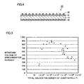
- Table 1 Furthermore, a relation between the total dislocation densities of the substrates in the semiconductor devices and withstand voltages of the semiconductor devices shown in Table 1 are compiled in Fig. 5 .
- each of the semiconductor devices exhibited a high withstand voltage of at least 400 V.
- the withstand voltage of the semiconductor devices drastically decreased when the total dislocation densities of the substrates became lower than 1 ⁇ 10 2 cm -2 , or became higher than 1 ⁇ 10 6 cm -2 .
- the withstand voltages of the semiconductor devices were stable at an extremely high level of 800-900 V.
- the screw dislocation density of the substrates in such semiconductor devices exceeded 1 x 10 4 cm -2 .
- the screw dislocation density of a substrate is preferably at most 1 x 10 4 cm -2 from a viewpoint of increasing a withstand voltage of the semiconductor device.
- the Al x Ga y In 1-x-y N crystal substrate according to the present invention can preferably be used as a substrate for various devices such as light-emitting elements, electronic element, and semiconductor sensors.
Landscapes
- Chemical & Material Sciences (AREA)
- Engineering & Computer Science (AREA)
- Crystallography & Structural Chemistry (AREA)
- Materials Engineering (AREA)
- Metallurgy (AREA)
- Organic Chemistry (AREA)
- Chemical Kinetics & Catalysis (AREA)
- General Chemical & Material Sciences (AREA)
- Inorganic Chemistry (AREA)
- Crystals, And After-Treatments Of Crystals (AREA)
- Led Devices (AREA)
Abstract
Description
- The present invention relates to an AlxGayIn1-x-yN crystal substrate (where x and y are numeric values satisfying 0 ≤ x, 0 ≤ y, and x + y ≤ 1, the same applies to the following) having a dislocation density for preferably being used as a substrate for various semiconductor devices such as light-emitting elements, electronic elements, and semiconductor sensors, a semiconductor device including the AlxGayIn1-x-yN crystal substrate, and a method of manufacturing the same.
- Group III nitride crystal substrates such as AlxGayIn1-x-yN crystal substrates are significantly useful as substrates for various semiconductor devices such as light-emitting elements, electronic elements, and semiconductor sensors. Here, in order to improve properties of the various semiconductor devices, there is a demand for AlxGayln1-x-yN crystal substrates each having a low dislocation density and favorable crystallinity. Further, from a viewpoint of utilization efficiency of the AlxGayIn1-x-yN crystal substrates, a main plane of each of the substrates is required to have an area of at least 10 cm-2, preferably at least 20 cm-2.
- Therefore, to fabricate the AlxGayIn1-x-yN crystal substrates each having a large size and a low dislocation density, various methods have been proposed in X. Xu and five others, "Growth and characterization of low defect GaN by hydride vapor phase epitaxy" J. Crystal Growth, 246, (2002), p223-229 (hereinafter referred to as Non-Patent Document 1), Japanese Patent Laying-Open No.
2001-102307 - Non-Patent
Document 1 discloses that in growth of a GaN crystal, for example, a dislocation density of the GaN crystal is decreased as a thickness of the grown crystal is increased. However, in such a method of decreasing a dislocation density by increasing the thickness to be grown, even if a GaN crystal is grown to have a thickness of 3 mm, it is difficult to decrease the dislocation density to 1 x 106 cm-2 or lower, and hence only a small effect of reducing dislocations is obtained. Furthermore, in such a method of decreasing a dislocation density, variations in dislocation density in a substrate plane also cause variations in dislocation density of a GaN crystal, and hence a region having a high dislocation density may remain in the GaN crystal. -
Patent Document 1 discloses a method of forming multiple pits each having a minute inclined plane, on a crystal growth plane, in growing a GaN crystal, and causing dislocations to occur intensively in these pits to thereby reduce dislocations in a region other than the pits. However, in such a method of decreasing a dislocation density, multiple pit regions each having a high dislocation density remain in a Group III nitride crystal. - Therefore, an AlxGayIn1-x-yN crystal substrate having a large size and a low dislocation density and suitably used for semiconductor devices has not yet been heretofore obtained.
- Patent Document 1: Japanese Patent Laying-Open No.
2001-102307 - Non-Patent Document 1: X. Xu and five others, "Growth and characterization of low defect GaN by hydride vapor phase epitaxy", J. Crystal Growth, 246, (2002), p223-229
- As a method of growing an AlxGayIn1-x-yN crystal for solving the above-described problems and obtaining an AlxGayIn1-x-yN crystal substrate having a large size and a low dislocation density, we proposed a crystal growth method characterized in that in growth of an AlxGayIn1-x-yN crystal, at least some of dislocations remaining in the AlxGayIn1-x-yN crystal are propagated in a direction substantially parallel to a crystal growth plane of the AlxGayIn1-x-yN crystal so as to be released to an outer periphery of the AlxGayIn1-x-yN crystal (e.g. see Patent Application No.
2005-316956 .). Accordingly, there was obtained an ability to grow an AlxGayIn1-x-yN crystal having a dislocation density of at most 1 x 106 cm-2, or at most 1 x 102 cm-2 depending on a condition, even in the case of a large-sized crystal having a main plane of at least 10 cm2, without allowing regions having a high dislocation density to remain. - Conventionally, there has been a belief that properties of a semiconductor device including an AlxGayIn1-x-yN crystal substrate are improved as a dislocation density of this substrate is decreased. However, when a property, for example, a withstand voltage (a voltage that causes a breakdown phenomenon of the semiconductor device, namely, a phenomenon of a drastic increase in current in a reverse direction; the same applies to the following) of a semiconductor device obtained by forming an at least one-layered semiconductor layer on the AlxGayIn1-x-yN crystal substrate obtained as such and having a low dislocation density was measured, it was found that an excessively low dislocation density of the substrate also lowers a withstand voltage of the semiconductor device.
- Therefore, inventors of the present invention fabricated semiconductor devices including AlxGayIn1-x-yN crystal substrates, respectively, which were obtained by the above-described crystal growth method and each of which had a dislocation density that fell within a range of 45 cm-2-3.2 × 106 cm-2 , and measured withstand voltages of the semiconductor devices. They thereby found a range of the dislocation density of the AlxGayIn1-x-yN crystal substrate for suitably being used for a semiconductor device, and has thus accomplished the present invention.
- In other words, an object of the present invention is to propose an AlxGayIn1-x-y N crystal substrate having a large size and a suitable dislocation density for serving as a substrate for a semiconductor device, a semiconductor device including the AlxGayIn1-x-y N crystal substrate, and a method of manufacturing the same.
- The present invention is an AlxGayIn1-x-yN crystal substrate (0 ≤ x, 0 ≤ y, x + y ≤ 1) which has a main plane having an area of at least 10 cm2. The main plane has an outer region located within 5 mm from an outer periphery of the main plane, and an inner region corresponding to a region other than the outer region. The inner region has a total dislocation density of at least 1 × 102 cm-2 and at most 1 × 106 cm-2.
- In the AlxGayIn1-x-yN crystal substrate according to the present invention, the total dislocation density can be set to at least 2 x 102 cm-2 and at most 1 × 105 cm-2. Furthermore, a screw dislocation density in the total dislocation density can be set to at most 1 × 104 cm-2 . Furthermore, the AlxGayIn1-x-yN crystal substrate according to the present invention can have n-type conductivity and have specific resistance of at most 1 Ω • cm. Furthermore, crystal growth of the AlxGayln1-x-yN crystal substrate according to the present invention can be performed by an HVPE method.
- Furthermore, the present invention is a semiconductor device including: an AlxGayln1-x-yN crystal substrate (0 ≤ x, 0 ≤ y, x + y ≤ 1); and an at least one-layered semiconductor layer formed on the AlxGayIn1-x-yN crystal substrate. The substrate has a main plane having an area of at least 10 cm2. The main plane has an outer region located within 5 mm from an outer periphery of the main plane, and an inner region corresponding to a region other than the outer region. The inner region has a total dislocation density of at least 1 x 102 cm-2 and at most 1 × 106 cm-2 . Furthermore, in the semiconductor device according to the present invention, the total dislocation density can be set to at least 2 × 102 cm-2 and at most 1 × 105 cm-2. Furthermore, a screw dislocation density in the total dislocation density can be set to at most 1 x 104 cm-2 .
- Furthermore, the present invention is a method of manufacturing a semiconductor device, including the steps of preparing an AlxGayIn1-x-yN crystal substrate (0 ≤ x, 0≤ y, x + y≤1 ); and growing an at least one-layered semiconductor layer on the substrate. The substrate has a main plane having an area of at least 10 cm2. The main plane has an outer region located within 5 mm from an outer periphery of the main plane, and an inner region corresponding to a region other than the outer region. The inner region has a total dislocation density of at least 1 × 102 cm-2 and at most 1 x 106 cm-2 . Furthermore, in the method of manufacturing the semiconductor device according to the present invention, the total dislocation density can be set to at least 2 x 102 cm-2 and at most 1 x 105 cm-2. Furthermore, a screw dislocation density in the total dislocation density can be set to at most 1 x 104 cm-2.
- According to the present invention, it is possible to provide an AlxGayln1-x-yN crystal substrate having a large size and a suitable dislocation density for serving as a substrate for a semiconductor device, a semiconductor device including the AlxGayIn1-x-y N crystal substrate, and a method of manufacturing the same.
-
-
Fig. 1 is a schematic cross-sectional view showing an embodiment of an AlxGayIn1-x-yN crystal substrate and a method of manufacturing the same, according to the present invention. Here, (a) shows a growing process of an AlxGayIn1-x-yN crystal, while (b) shows a process of manufacturing the AlxGayIn1-x-yN crystal substrate. -
Fig. 2 is a schematic view showing an HVPE apparatus used for growing the AlxGayIn1-x-yN crystal in the present invention. -
Fig. 3A is a schematic plan view showing a base substrate used for growing the AlxGayIn1-x-yN crystal in the present invention. -
Fig. 3B is a schematic side view of the base substrate shown inFig. 3A . -
Fig. 3C is a schematic cross-sectional view of the base substrate shown inFig. 3A taken along IIIC-IIIC. -
Fig. 4 is a schematic cross-sectional view showing an embodiment of a semiconductor device according to the present invention. -
Fig. 5 is a diagram showing a relation between total dislocation densities of substrates in the semiconductor devices and withstand voltages of the semiconductor devices. - 10: base substrate, 10m, 12m: main plane, 10p: apex, 10s: (0001) plane, 11: AlxGayIn1-x-yN crystal, 11a, 11b, 11c, 11s: crystal growth plane, 11d: dislocation propagation line, 11r: crystal growth starting plane, 11t: macro step plane, 11v, 12v: outer periphery, 12, 12a, 12b, 12c, 12d, 12e: AlxGayIn1-x-yN crystal substrate, 12n: inner region, 12w: outer region, 21: HCl gas, 22: gallium, 23: gallium chloride gas, 26: nitrogen source gas, 29: doping gas, 40: semiconductor device, 41: semiconductor layer, 42: Schottky electrode, 43: ohmic electrode, 101m, 102m, 103m: partial plane, 200: HVPE apparatus, 201: reaction chamber, 202: substrate holder, 203: gallium chloride synthesis chamber, 204: gallium boat, 205: HCl gas conduit, 206: nitrogen source gas conduit, 207: exhaust pipe, 208, 209, 210: heater, R: radius, T: thickness, θ: inclined angle, φ: dislocation propagation angle.
- With reference to
Fig. 1 , an embodiment of an AlxGayIn1-x-yN crystal substrate 12 according to the present invention is a large-sized substrate that has amain plane 12m having an area of at least 10 cm2.Main plane 12m has anouter region 12w located within 5 mm from anouter periphery 12v, and aninner region 12n corresponding to a region other than the outer region.Inner region 12n has a total dislocation density of at least 1 × 102 cm-2 and at most 1 × 106 cm-2. - AlxGayIn1-x-y
N crystal substrate 12 according to the present embodiment hasmain plane 12m having an area of at least 10cm2, and hence can be applied to a wide variety of semiconductor devices and has high utilization efficiency. - Furthermore, AlxGayIn1-x-y
N crystal substrate 12 according to the present embodiment hasinner region 12n having a total dislocation density of at least 1 x 102 cm-2 and at most 1 × 106 cm-2, and hence properties of a semiconductor device obtained by growing an at least one-layered semiconductor layer onsubstrate 12 are improved. Here, a region where a total dislocation density is evaluated is set toinner region 12 corresponding to a region other thanouter region 12w because dislocations tend to remain in the outer region, and if a semiconductor device is fabricated in the inner region corresponding to a region other than the outer region having a high dislocation density, the effect thereof can be ignored. It is of course more preferable that the outer region also has fewer dislocations. - Examples of dislocations that can be exhibited in a substrate include a screw dislocation, an edge dislocation, and a mixed dislocation including the screw dislocation and the edge dislocation in a mixed manner. A dislocation that appears in a substrate can be observed as a pit generated by etching the substrate. Although an etchant is not particularly limited, a mixed melt of KOH and NaOH, having a liquid temperature of approximately 300-500°C (hereinafter referred to as a KOH-NaOH mixed melt), or a mixed liquid of phosphoric acid and sulfuric acid, having a liquid temperature of approximately 200-300°C (hereinafter referred to as a phosphoric acid-sulfuric acid mixed liquid), is preferably used. The dislocation density can be calculated by counting the number of pits per unit area.
- When the substrate is etched, a dislocation site appears as a pit, and according to the size of the pit, the types of dislocation can be identified. A large pit (hereinafter referred to as an L pit) is derived from a screw dislocation, while a small pit (hereinafter referred to as an S pit) is derived from an edge dislocation. An intermediate-sized pit (hereinafter referred to as an I pit) is derived from a mixed dislocation. An absolute value of the size of each pit varies depending on a condition for etching a substrate. However, a ratio of relative sizes of the L pit, the I pit, and the S pit is approximately constant without depending on an etching condition. A ratio of (an L pit diameter) : (an I pit diameter) : (an S pit diameter) is approximately 10 : 2 : 1.
- In the present application, the dislocation refers to any of the above-described screw dislocation, edge dislocation, and mixed dislocation, and total dislocations refer to all the dislocations including the above-described screw dislocation, edge dislocation, and mixed dislocation. Therefore, the total dislocation density is the number of total dislocations per unit area, namely, a sum of the numbers of screw dislocations, edge dislocations, and mixed dislocations per unit area, and is calculated by counting the total numbers of L pits, I pits, and S pits per unit area. In other words, the total dislocation density is a sum of a screw dislocation density, an edge dislocation density, and a mixed dislocation density. The screw pit density is the number of screw dislocations per unit area, and is calculated by counting the number ofL pits per unit area.
- Conventionally, there has been a belief that properties of a semiconductor device including a substrate are improved as a dislocation density of the substrate is decreased. However, if a total dislocation density of the substrate becomes an ultralow dislocation density of less than 1 x 102 cm-2, properties of the semiconductor device are degraded instead. Although the reason thereof is not elucidated clearly at present, an inference is made as follows. Specifically, a dislocation has a function of an opening (also referred to as a getter; the same applies to the following) for drawing in precipitates generated owing to impurities or variations in composition of the substrate, and if the number of such dislocations is excessively decreased, generation of the above-described precipitates cannot be suppressed, causing degradation in crystallinity of the substrate.
- If the total dislocation density of the substrate exceeds 1 x 106 cm-2, dislocations of the crystal are increased and crystallinity is lowered, resulting in degradation of properties of the semiconductor device. Therefore, a total dislocation density of the substrate that improves properties of the semiconductor device is at least 1 x 102 cm-2 and at most 1 x 106 cm-2. From the above-described viewpoint, the total dislocation density of the substrate is preferably at least 2 × 102 cm-2 and at most 1 x 105 cm-2.
- As to the screw dislocation density in the total dislocation density of the AlxGayI1-x-yN crystal substrate in the present embodiment, the screw dislocation density of the inner region is preferably at most 1 × 104 cm-2 from a viewpoint of improving properties of a semiconductor device including the substrate. In other words, as long as the total dislocation density is at least 1 x 102 cm-2 and at most 1 x 106 cm-2, a lower screw dislocation density is more preferable, and a screw dislocation density of 0 cm-2 may also be possible.
- The degradation in properties of the semiconductor device caused by decreasing the total dislocation density of the AlxGayIn1-x-yN crystal substrate in the present embodiment to less than 1 x 102 cm-2, becomes significant as the substrate has higher conductivity. In contrast, if the AlxGayIn1-x-yN crystal substrate has n-type conductivity and has specific resistance of at most 1 Ω • cm, an effect of improving properties of the semiconductor device by setting the total dislocation density of the substrate to at least 1 x 102 cm-2 and at most 1 x 106 cm-2 is remarkably exhibited.
- Crystal growth of the AlxGayIn1-x-yN crystal substrate in the present embodiment is preferably performed by an HVPE method, from a viewpoint of easily obtaining a thick crystal and increasing a yield of the substrate.
- A large-sized AlxGayIn1-x-yN crystal substrate which has a main plane having an area of at least 10 cm2 and has an inner region having a total dislocation density of at least 1x102 cm-2 and at most 1 × 106 cm-2, as shown in the present embodiment, can be fabricated as follows.
- Initially, with reference to
Fig. 1 (a) , an AlxGayIn1-x-yN crystal is grown, for example, as described below. There are included the steps of preparing, as abase substrate 10, an inclined substrate which has amain plane 10m having an inclined angle θ of at least 0.5° and at most 10° with respect tocrystal growth planes main plane 10m of the inclined substrate. Accordingly, when AlxGayIn1-x-yN crystal 11 is grown, at least some of dislocations inherited frommain plane 10m ofbase substrate 10 and remaining in AlxGayIn1-x-yN crystal 11 are propagated in a direction substantially parallel tocrystal growth planes Fig. 1 shows a path along which the dislocations are propagated, as adislocation propagation line 11d.) and released to anouter periphery 1 1v of AlxGayIn1-x-yN crystal 11, so that a total dislocation density is adjusted to at least 1 × 102 cm-2 and at most 1 x 106 cm-2 . Note that inFig. 1 (a) ,crystal growth planes crystal growth plane 11 s represents a crystal growth plane after crystal growth. - In other words, with reference to
Fig. 1 (a) , the present invention is as follows. AlxGayIn1-x-yN crystal 11 is grown on the inclined substrate which hasmain plane 10m having inclined angle θ of at least 0.5° and at most 10° with respect tocrystal growth planes N crystal 11. During the growth, amacro step plane 11t substantially perpendicular tocrystal growth planes crystal growth planes macro step plane 11t moves toouter periphery 11v of the crystal and disappears. It was found that the dislocations in the crystal propagate in a direction substantially parallel tocrystal growth planes macro step plane 11 t, and are released to an outside of the crystal asmacro step plane 11t moves toouter periphery 11v of the crystal. This phenomenon is applied to a method of growing AlxGayIn1-x-yN crystal 11, so that it is possible to grow AlxGayIn1-x-yN crystal 11 having a total dislocation density of at least 1 × 102 cm-2 and at most 1 × 106 cm-2 without allowing a region having a high total dislocation density to remain in the crystal. - Here, if inclined angle θ is less than 0.5°, the macro step plane is less likely to be formed, and propagation of the dislocations in the direction substantially perpendicular to the macro step plane becomes difficult. If inclined angle θ exceeds 10°, a stable crystal growth plane is less likely to be formed, and propagation of the dislocations in the direction substantially parallel to the crystal growth plane becomes difficult. In view of the foregoing, inclined angle θ is preferably larger than 2° and smaller than 8°.
- During crystal growth, the crystal growth plane is parallel-translated in the direction of its normal as the crystal grows, as shown by
crystal growth plane 11a,crystal growth plane 11b,crystal growth plane 11c, andcrystal growth plane 11s, while causingmacro step plane 11t to gradually disappear, as described above. Therefore, a direction ofdislocation propagation line 11d (which refers to a line showing a path along which dislocations are propagated; the same applies to the following) has a certain dislocation propagation angle φ with respect to a crystal growth plane arbitrarily specified. Such dislocation propagation angle φ is determined by a dislocation propagation rate and a crystal growth rate. The dislocation propagation angle becomes smaller as the dislocation propagation rate becomes high with respect to the crystal growth rate. In such a method of growing AlxGayIn1-x-yN crystal 11, the dislocation propagation rate is approximately equal to a moving rate of the macro step plane, and the moving rate of such a step plane becomes at least 5 times, and furthermore, at least 10 times as high as the crystal growth rate (i.e. the moving rate of the crystal growth plane) depending on a crystal growth condition. Consequently, the above-described dislocation propagation angle is at most 11°, and furthermore, at most 5.5°. - Accordingly, in the present application, "the direction substantially parallel to the crystal growth plane" means "a direction along an inclined angle falling within a range of 0°-11° with respect to the crystal growth plane", and "the direction substantially perpendicular to the macro step plane" means "a direction along an inclined angle falling within a range of 79°-90° with respect to the macro step plane".
- As to the above-described inclined substrate (base substrate 10), it is preferable to use an AlPGaqIn1-p-qN substrate (0 ≤ p, 0 ≤ q, p + q≤ 1; the same applies to the following) from a viewpoint of lattice continuity between the inclined substrate and AlxGayIn1-x-yN crystal 11 to be grown. Here, x and p may be the same numeric value or different numeric values, and y and q may be the same numeric value or different numeric values. However, a combination that achieves lattice continuity is of course preferable. Here, if x and p are the same numeric value and y and q are the same numeric value, lattice continuity is of course obtained. However, even a combination in which at least one of a pair of x and p and a pair of y and q is different numeric values also achieves lattice continuity, and hence such a combination may be used. Furthermore, from a viewpoint of obtaining a crystal having favorable crystallinity at a high growth rate, it is preferable to grow a (0001) plane as the crystal growth plane of AlxGayIn1-x-yN crystal 11 to be grown.
- With reference to
Fig. 1 (b) , AlxGayIn1-x-yN crystal 11 obtained as described above is cut into flat planes, and their main planes are polished, so that at least one AlxGayIn1-x-yN crystal substrate 12 is formed. - With reference to
Fig. 4 , an embodiment of asemiconductor device 40 according to the present invention issemiconductor device 40 including AlxGayIn1-x-yN crystal substrate 12 and an at least one-layeredsemiconductor layer 41 formed thereon.Substrate 12 hasmain plane 12m having an area of at least 10 cm2.Main plane 12m hasouter region 12w located within 5 mm from its outer periphery andinner region 12n corresponding to a region other than the outer region.Inner region 12n has a total dislocation density of at least 1 x 102 cm-2 and at most 1 × 106 cm-2. The semiconductor device in the present embodiment includes the AlxGayIn1-x-yN crystal substrate in the first embodiment, and hence has high properties. - Although such a semiconductor device is not particularly limited, examples thereof include light-emitting elements such as a light-emitting diode and a laser diode, electronic elements such as a rectifier, a bipolar transistor, a field-effect transistor, and an HEMT (High Electron Mobility Transistor), semiconductor sensors such as a temperature sensor, a pressure sensor, a radiation sensor, and a visible-ultraviolet light detector, an SAW (Surface Acoustic Wave) device, a vibrator, a resonator, an oscillator, an MEMS (Micro Electro Mechanical System) part, a voltage actuator, and others.
- With reference to
Fig. 4 , a method of manufacturing a semiconductor device in the present embodiment includes the steps of preparing AlxGayIn1-x-yN crystal substrate 12, and growing at least one-layeredsemiconductor layer 41 onsubstrate 12.Substrate 12 hasmain plane 12m having an area of at least 10 cm2.Main plane 12m hasouter region 12w located within 5 mm from its outer periphery, andinner region 12n corresponding to a region other than the outer region.Inner region 12n has a total dislocation density of at least 1 x 102 cm-2 and at most 1 x 106 cm-2. According to such a manufacturing method, it is possible to obtain a semiconductor device having high properties by growing at least one-layeredsemiconductor layer 41 on AlxGayIn1-x-yN crystal substrate 12 in the first embodiment. Here the step of preparing the AlxGayIn1-x-yN crystal substrate may include the steps shown in the first embodiment, namely, as shown inFig. 1 (a) , may include the steps of preparing a prescribed inclined substrate asbase substrate 10, and growing AlxGayIn1-x-yN crystal substrate 11 onmain plane 10m of this inclined substrate, and as shown inFig. 1 (b) , may include the steps of cutting AlxGayIn1-x-yN crystal substrate 11 into flat planes, and polishing their main planes and forming AlxGayIn1-x-yN crystal substrates 12. - A GaN crystal substrate identified as an AlxGayIn1-x-yN crystal substrate was fabricated by an HVPE method. With reference to
Fig. 2 , in anHVPE apparatus 200 used in the present example, asubstrate holder 202 for holdingbase substrate 10 is arranged in areaction chamber 201, and there are installed a galliumchloride synthesis chamber 203 for synthesizing agallium chloride gas 23 to be introduced intoreaction chamber 201, anHCl gas conduit 205 for introducing anHCl gas 21 into galliumchloride synthesis chamber 203, a nitrogensource gas conduit 206 for introducing anitrogen source gas 26 and if necessary, adoping gas 29, intoreaction chamber 201, and anexhaust pipe 207 for exhausting reacted gases. Furthermore, agallium boat 204 accommodating gallium (Ga) 22 is arranged in galliumchloride synthesis chamber 203. Furthermore, around galliumchloride synthesis chamber 203 andreaction chamber 201, there areinstalled heaters heating HCl gas 21,nitrogen source gas 26, dopinggas 29,gallium boat 204,base substrate 10, and others. - In
HVPE apparatus 200 described above,gallium chloride gas 23 to be introduced intoreaction chamber 201 is synthesized as follows. Specifically,gallium boat 204 arranged in galliumchloride synthesis chamber 203 is heated to 800°C byheater 209,HCl gas 21 is introduced into galliumchloride synthesis chamber 203 throughHCl gas conduit 205, andHCl gas 21 is made to react with gallium (Ga) 22 ingallium boat 204, to thereby synthesize a GaCl gas (gallium chloride gas 23). Here,HCl gas 21 is introduced into galliumchloride synthesis chamber 203, along with a carrier gas such as an H2 gas. - The above-described GaCl gas (gallium chloride gas 23), an NH3 gas (nitrogen source gas 26), and an SiH4 gas (doping gas 29) were introduced into
reaction chamber 201 along with an H2 gas serving as a carrier gas. On the GaN substrate (base substrate 10) arranged onsubstrate holder 202 inreaction chamber 201 and heated to a substrate temperature of 1200°C, the GaCl gas (gallium chloride gas 23) was made to react with an NH3 gas (nitrogen source gas 26) to grow a GaN crystal for 100 hours. As shown inFig. 1 (a) , there is obtained a GaN crystal (AlxGayIn1-x-yN crystal 11) doped with Si and having a thickness T of 5 mm from an apex 10p ofbase substrate 10. - When the GaN crystal was grown, in order to improve uniformity of an amount of each of the GaCl gas (gallium chloride gas 23) and the NH3 gas (nitrogen source gas 26) supplied to the main plane of the GaN substrate, the GaN substrate (base substrate 10) was arranged on
substrate holder 202 such that it was inclined 10° with respect to a horizontal plane, and rotated at a revolution speed of 60 revolutions/min. Furthermore, the partial pressure of the GaCl gas (gallium chloride gas 23) was set to 5.065 kPa (0.05 atm), the partial pressure of the NH3 gas (nitrogen source gas 26) was set to 10.13 kPa (0.1 atm), and the partial pressure of the SiH4 gas (doping gas 29) was set to 5.065 Pa (0.00005 atm). - Here, as
base substrate 10, as shown inFigs. 3A-3C , there were used five GaN substrates having different inclined heights H. Each of the five GaN substrates hadmain plane 10m where a crystal was to be grown, processed into a triangular pyramidshape having apex 10p and threepartial planes Figs. 3A, 3B and 3C show a <10-10> direction, a <0001> direction, and the <0001> direction, respectively. Inbase substrate 10, as is clear fromFigs. 3B and 3C , inclined angle θ, which is formed by each ofpartial planes - Next, as shown in
Fig. 1 (b) , the GaN crystal (AlxGayIn1-x-yN crystal 11) grown on the GaN substrate (base substrate 10) was sliced into pieces on planes parallel to the (0001) plane, and main planes of the pieces were polished, to thereby obtain five GaN crystal substrates (AlxGayIn1-x-yN crystal substrate 12) each having a thickness of 0.5 mm. The five GaN crystal substrates obtained from the GaN crystal grown on base substrate I are referred to as a substrate I-a (AlxGayIn1-x-yN crystal substrate 12a), a substrate I-b (AlxGayIn1-x-yN crystal substrate 12b), a substrate I-c (AlxGayln1-x-yN crystal substrate 12c), a substrate I-d (AlxGayIn1-x-yN crystal substrate 12d), and a substrate I-e (AlxGayIn1-x-yN crystal substrate 12e), in the order closer to base substrate I. Similarly, the five GaN crystal substrates obtained from the GaN crystal grown on base substrate II are referred to as a substrate II-a, a substrate II-b, a substrate II-c, a substrate II-d, and a substrate II-e, in the order closer to base substrate II. The five GaN crystal substrates obtained from the GaN crystal grown on base substrate III are referred to as a substrate m-a, a substrate m-b, a substrate m-c, a substrate III-d, and a substrate III-e, in the order closer to base substrate III. The five GaN crystal substrates obtained from the GaN crystal grown on base substrate IV are referred to as a substrate IV-a, a substrate IV-b, a substrate IV-c, a substrate IV-d, and a substrate IV-e, in the order closer to base substrate IV. Specific resistance of these GaN crystal substrates was 0.03-0.08 Ω • cm by an eddy-current conductivity measurement. - Each of the GaN crystal substrates obtained as described above was etched with a KOH-NaOH mixed melt at a liquid temperature of 350°C, to form pits derived from various dislocations. The total number of pits per unit area was counted to thereby calculate the total dislocation density. In calculation of the total dislocation density, an area of the calculation region was adjusted such that 100-500 pits were observed in the calculation region, depending on the total dislocation density. Note that the maximum area of the calculation region was set to 1 cm2. Furthermore, in calculation of the total dislocation density, a plurality of calculation regions were provided in the inner region of each of the substrates, and a mean value of total dislocation densities calculated from the plurality of calculation regions is shown in Table 1. The screw dislocation density was calculated in a manner similar to that of the calculation of the total dislocation density, except for that the screw dislocation density was calculated by counting the number of L pits per unit area. There existed a distribution of the total dislocation densities and a distribution of the screw dislocation densities in the inner region of the main plane. However, even in a part having the highest density, its density was at most two times as high as a mean value of each of the total dislocation densities and the screw dislocation densities.
[Table 1 ] Substrate Dislocation Density of Substrate Properties of Semiconductor Device Total Dislocation Density Screw Dislocation Density Withstand Voltage (V) (cm-2) (cm-2) I-a 3200000 110000 360 I-b 1100000 56000 400 I-c 370000 28000 470 I-d 98000 28000 560 I-e 81000 12000 680 II-a 1300000 6200 450 II-b 350000 9800 680 II-c 3500 7300 840 II-d 2500 1200 880 II-e 2200 500 900 III-a 170000 200 750 III-b 2500 2700 860 III-c 1200 750 840 III- d 600 350 880 III- e 200 100 810 IV-a 41000 0 820 IV- b 500 120 800 IV-c 110 0 670 IV-d 52 0 250 IV-e 45 0 200 - As is clear from Table 1, the total dislocation density and the screw dislocation density of a substrate tend to decrease as
base substrate 10 used for crystal growth has larger inclined height H, and as the substrate is located farther frombase substrate 10. In other words, it is possible to adjust the total dislocation density and the screw dislocation density in a crystal, by inclined height H ofbase substrate 10 and/or a thickness of the AlxGayIn1-x-yN crystal to be grown. - Each of the substrates etched in the first example was polished again, to thereby form GaN crystal substrates each having a diameter of 5.08 cm x a thickness of 400 µm (with specific resistance of 0.03-0.08Ω • cm). With reference to
Fig. 4 , an n-type GaN layer (semiconductor layer 41) having a thickness of 15 µm and a carrier density of 1 x 1016 cm-3 was then grown as a semiconductor layer by an MOCVD method on each of the substrates (AlxGayIn1-x-yN crystal substrate 12). Next,Schottky electrodes 42 each having a diameter of 450 µm and configured with an Au layer were formed on the n-type GaN layer (semiconductor layer 41) by a vacuum deposition method, at a pitch of 2 mm, and anohmic electrode 43 configured with a layered body of a Ti layer and an Al layer was formed on the entire plane of each of the substrates (AlxGayIn1-x-yN crystal substrate 12) where the n-type GaN layer was not formed, and thussemiconductor devices 40 were obtained. - A voltage in an inverse direction was applied between
Schottky electrodes 42 andohmic electrode 43 of eachsemiconductor device 40 obtained, and a withstand voltage (a voltage that causes a phenomenon of a drastic increase in current in a reverse direction) of eachsemiconductor device 40 was measured. As to each of the semiconductor devices, the withstand voltage was measured at 19 points, and the mean value thereof was set as a withstand voltage of the semiconductor device. The results are compiled in Table 1. Furthermore, a relation between the total dislocation densities of the substrates in the semiconductor devices and withstand voltages of the semiconductor devices shown in Table 1 are compiled inFig. 5 . - As is clear from Table 1 and
Fig. 5 , in the range of the total dislocation densities of the substrates in the semiconductor devices of at least 1 × 102 cm-2 and at most 1 × 106 cm-2, each of the semiconductor devices exhibited a high withstand voltage of at least 400 V. In other words, the withstand voltage of the semiconductor devices drastically decreased when the total dislocation densities of the substrates became lower than 1 × 102 cm-2, or became higher than 1 × 106 cm-2. Furthermore, in the range of the total dislocation density of the substrates in the semiconductor devices of at least 2 x 102 cm-2 and at most 1 x 105 cm-2, the withstand voltages of the semiconductor devices were stable at an extremely high level of 800-900 V. In other words, in the range of the total dislocation density of the substrates of at least 2 x 102 cm-2 and at most 1 x 105 cm-2, it was possible to obtain a semiconductor device having a uniform and high withstand voltage regardless of a value of the total dislocation density. - In
Fig. 5 , even in the range of the total dislocation density of the substrates in the semiconductor devices of at least 1 × 102 cm-2 and at most 1 × 106 cm-2, the semiconductor devices fabricated with the use of substrate I-c, substrate I-d, and substrate I-e, respectively, as substrates, exhibited low withstand voltages. The screw dislocation density of the substrates in such semiconductor devices exceeded 1 x 104 cm-2. In other words, the screw dislocation density of a substrate is preferably at most 1 x 104 cm-2 from a viewpoint of increasing a withstand voltage of the semiconductor device. - It should be understood that the embodiments and examples disclosed herein are illustrative and not limitative in all aspects. The scope of the present invention is shown not by the description above but by the scope of the claims, and is intended to include all modifications within the equivalent meaning and scope of the claims. INDUSTRIAL APPLICABILITY
- The AlxGayIn1-x-yN crystal substrate according to the present invention can preferably be used as a substrate for various devices such as light-emitting elements, electronic element, and semiconductor sensors.
Claims (14)
- An AlxGayIn1-x-yN crystal substrate (0 ≤ x, 0 ≤ y, x + y ≤1) (12) which has a main plane (12m) having an area of at least 10 cm2, wherein
said main plane (12m) has an outer region (12w) located within 5 mm from an outer periphery of said main plane, and an inner region (12n) corresponding to a region other than said outer region, and
said inner region (12n) has a total dislocation density of at least 1 × 102 cm-2 and at most 1 × 106 cm-2. - The AlxGayIn1-x-yN crystal substrate according to claim 1, wherein said total dislocation density is at least 2 × 102 cm-2 and at most 1 x 105 cm-2.
- The AlxGayIn1-x-yN crystal substrate according to claim 2, wherein a screw dislocation density in said total dislocation density is at most 1 x 104 cm-2.
- The AlxGayIn1-x-yN crystal substrate according to claim 1, wherein a screw dislocation density in said total dislocation density is at most 1 x 104 cm-2.
- The AlxGayIn1-x-yN crystal substrate according to claim 1, wherein said substrate (12) has n-type conductivity and has specific resistance of at most 1 Ω • cm.
- The AlxGayIn1-x-yN crystal substrate according to claim 1, wherein crystal growth of said substrate (12) is performed by an HVPE method.
- A semiconductor device (40) comprising: an AlxGayIn1-x-yN crystal substrate (0 ≤ x, 0 ≤ y, x + y ≤ 1) (12); and an at least one-layered semiconductor layer (41) formed on said AlxGayIn1-x-yN crystal substrate, wherein
said substrate (12) has a main plane (12m) having an area of at least 10 cm2,
said main plane (12m) has an outer region (12w) located within 5 mm from an outer periphery of said main plane, and an inner region (12n) corresponding to a region other than said outer region, and
said inner region (12n) has a total dislocation density of at least 1 × 102 cm-2 and at most 1 × 106 cm-2. - The semiconductor device according to claim 7, wherein said total dislocation density is at least 2 x 102 cm-2 and at most 1 x 105 cm-2.
- The semiconductor device according to claim 8, wherein a screw dislocation density in said total dislocation density is at most 1 × 104 cm-2.
- The semiconductor device according to claim 7, wherein a screw dislocation density in said total dislocation density is at most 1 x 104 cm-2.
- A method of manufacturing a semiconductor device, comprising the steps of preparing an AlxGayIn1-x-yN crystal substrate (0≤ x, 0 ≤ y, x + y ≤ 1) (12); and growing an at least one-layered semiconductor layer (41) on said substrate (12), wherein
said substrate (12) has a main plane (12m) having an area of at least 10 cm2,
said main plane (12m) has an outer region (12w) located within 5 mm from an outer periphery of said main plane, and an inner region (12n) corresponding to a region other than said outer region, and
said inner region (12n) has a total dislocation density of at least 1 × 102 cm-2 and at most 1 × 106 cm-2. - The method of manufacturing the semiconductor device according to claim 11, wherein said total dislocation density is at least 2 x 102cm-2 and at most 1 x 105 cm-2.
- The method of manufacturing the semiconductor device according to claim 12, wherein a screw dislocation density in said total dislocation density is at most 1 x 104 cm-2.
- The method of manufacturing the semiconductor device according to claim 11, wherein a screw dislocation density in said total dislocation density is at most 1 x 104 cm-2 .
Applications Claiming Priority (2)
| Application Number | Priority Date | Filing Date | Title |
|---|---|---|---|
| JP2005360621A JP2007161536A (en) | 2005-12-14 | 2005-12-14 | AlxGayIn1-xyN crystal substrate, semiconductor device and manufacturing method thereof |
| PCT/JP2006/320549 WO2007069388A1 (en) | 2005-12-14 | 2006-10-16 | AlxGayIn1-x-yN CRYSTAL SUBSTRATE, SEMICONDUCTOR DEVICE, AND METHOD FOR MANUFACTURING THE SAME |
Publications (2)
| Publication Number | Publication Date |
|---|---|
| EP1970946A1 true EP1970946A1 (en) | 2008-09-17 |
| EP1970946A4 EP1970946A4 (en) | 2011-09-07 |
Family
ID=38162703
Family Applications (1)
| Application Number | Title | Priority Date | Filing Date |
|---|---|---|---|
| EP06811820A Withdrawn EP1970946A4 (en) | 2005-12-14 | 2006-10-16 | AlxGayIn1-x-yN CRYSTALLINE SUBSTRATE, SEMICONDUCTOR DEVICE AND METHOD FOR MANUFACTURING THE SAME |
Country Status (9)
| Country | Link |
|---|---|
| US (1) | US7943964B2 (en) |
| EP (1) | EP1970946A4 (en) |
| JP (1) | JP2007161536A (en) |
| KR (1) | KR20080083285A (en) |
| CN (2) | CN101331591B (en) |
| CA (1) | CA2633118A1 (en) |
| RU (1) | RU2401481C2 (en) |
| TW (1) | TW200729301A (en) |
| WO (1) | WO2007069388A1 (en) |
Cited By (2)
| Publication number | Priority date | Publication date | Assignee | Title |
|---|---|---|---|---|
| EP2067884A1 (en) * | 2007-11-30 | 2009-06-10 | Sumitomo Electric Industries, Ltd. | III Nitride crystal substrate, and light-emitting device and method of its manufacture |
| CN102187433A (en) * | 2008-10-24 | 2011-09-14 | 住友电气工业株式会社 | Iii nitride semiconductor electronic device, method for manufacturing iii nitride semiconductor electronic device, and iii nitride semiconductor epitaxial wafer |
Families Citing this family (10)
| Publication number | Priority date | Publication date | Assignee | Title |
|---|---|---|---|---|
| JP2009051686A (en) * | 2007-08-24 | 2009-03-12 | Sumitomo Electric Ind Ltd | Group III nitride crystal growth method |
| JP5139010B2 (en) * | 2007-09-06 | 2013-02-06 | 住友電気工業株式会社 | Group III nitride crystal growth method |
| JP5144192B2 (en) * | 2007-09-21 | 2013-02-13 | 住友電気工業株式会社 | Group III nitride crystal growth method |
| WO2009070625A1 (en) * | 2007-11-27 | 2009-06-04 | Nanocrystal, Llc | Ultra-low dislocation density group iii - nitride semiconductor substrates grown via nano-or micro-particle film |
| JP4924498B2 (en) * | 2008-03-18 | 2012-04-25 | 住友電気工業株式会社 | Nitride-based semiconductor light-emitting device, epitaxial wafer, and method for manufacturing nitride-based semiconductor light-emitting device |
| JP5045589B2 (en) * | 2008-07-18 | 2012-10-10 | 住友電気工業株式会社 | Group III nitride crystal growth method |
| CN102119443B (en) * | 2008-08-05 | 2013-08-14 | 住友电气工业株式会社 | Schottky barrier diode and method of manufacturing a Schottky barrier diode |
| CN103367573B (en) * | 2013-05-23 | 2016-07-06 | 台州市一能科技有限公司 | Opto-electronic semiconductor module |
| CN111630630A (en) * | 2017-11-10 | 2020-09-04 | 晶化成半导体公司 | Large-size ultraviolet transparent aluminum nitride single crystal and preparation method thereof |
| JP6998798B2 (en) * | 2018-03-02 | 2022-01-18 | 株式会社サイオクス | GaN laminate and its manufacturing method |
Family Cites Families (13)
| Publication number | Priority date | Publication date | Assignee | Title |
|---|---|---|---|---|
| JPS57120343A (en) | 1981-01-19 | 1982-07-27 | Oki Electric Ind Co Ltd | Manufacture of substrate for semiconductor element |
| US6440823B1 (en) * | 1994-01-27 | 2002-08-27 | Advanced Technology Materials, Inc. | Low defect density (Ga, Al, In)N and HVPE process for making same |
| US5668395A (en) * | 1994-11-22 | 1997-09-16 | Northwestern University | Composition for InSB and GaAs thin film on silicon substrate for use in photodetectors |
| JP2000188285A (en) * | 1998-10-13 | 2000-07-04 | Sony Corp | Etching method, crystallinity evaluation method, and semiconductor device manufacturing method |
| JP4145437B2 (en) | 1999-09-28 | 2008-09-03 | 住友電気工業株式会社 | Single crystal GaN crystal growth method, single crystal GaN substrate manufacturing method, and single crystal GaN substrate |
| RU2187172C1 (en) * | 2001-01-09 | 2002-08-10 | Фонд поддержки науки и образования | Method for producing epitaxial layer of iii- nitride superconductor on foreign substrate |
| US6806508B2 (en) * | 2001-04-20 | 2004-10-19 | General Electic Company | Homoepitaxial gallium nitride based photodetector and method of producing |
| JP3801125B2 (en) * | 2001-10-09 | 2006-07-26 | 住友電気工業株式会社 | Single crystal gallium nitride substrate, method for crystal growth of single crystal gallium nitride, and method for manufacturing single crystal gallium nitride substrate |
| JP3864870B2 (en) * | 2001-09-19 | 2007-01-10 | 住友電気工業株式会社 | Single crystal gallium nitride substrate, growth method thereof, and manufacturing method thereof |
| US7309534B2 (en) * | 2003-05-29 | 2007-12-18 | Matsushita Electric Industrial Co., Ltd. | Group III nitride crystals usable as group III nitride substrate, method of manufacturing the same, and semiconductor device including the same |
| US7323256B2 (en) * | 2003-11-13 | 2008-01-29 | Cree, Inc. | Large area, uniformly low dislocation density GaN substrate and process for making the same |
| US7687827B2 (en) * | 2004-07-07 | 2010-03-30 | Nitronex Corporation | III-nitride materials including low dislocation densities and methods associated with the same |
| JP5162895B2 (en) * | 2006-01-12 | 2013-03-13 | 住友電気工業株式会社 | Aluminum nitride crystal manufacturing method, aluminum nitride crystal, aluminum nitride crystal substrate, and semiconductor device |
-
2005
- 2005-12-14 JP JP2005360621A patent/JP2007161536A/en active Pending
-
2006
- 2006-10-16 US US12/096,986 patent/US7943964B2/en active Active
- 2006-10-16 KR KR1020087015068A patent/KR20080083285A/en not_active Withdrawn
- 2006-10-16 EP EP06811820A patent/EP1970946A4/en not_active Withdrawn
- 2006-10-16 WO PCT/JP2006/320549 patent/WO2007069388A1/en not_active Ceased
- 2006-10-16 CN CN2006800474800A patent/CN101331591B/en not_active Expired - Fee Related
- 2006-10-16 CA CA002633118A patent/CA2633118A1/en not_active Abandoned
- 2006-10-16 CN CN201010163633A patent/CN101847575A/en active Pending
- 2006-10-16 RU RU2008128490/28A patent/RU2401481C2/en not_active IP Right Cessation
- 2006-11-29 TW TW095144181A patent/TW200729301A/en unknown
Cited By (4)
| Publication number | Priority date | Publication date | Assignee | Title |
|---|---|---|---|---|
| EP2067884A1 (en) * | 2007-11-30 | 2009-06-10 | Sumitomo Electric Industries, Ltd. | III Nitride crystal substrate, and light-emitting device and method of its manufacture |
| CN102187433A (en) * | 2008-10-24 | 2011-09-14 | 住友电气工业株式会社 | Iii nitride semiconductor electronic device, method for manufacturing iii nitride semiconductor electronic device, and iii nitride semiconductor epitaxial wafer |
| EP2346068A4 (en) * | 2008-10-24 | 2013-06-12 | Sumitomo Electric Industries | NITRIDE III SEMICONDUCTOR ELECTRONIC DEVICE, METHOD FOR MANUFACTURING III NITRIDE SEMICONDUCTOR ELECTRONIC DEVICE, AND III NITRIDE SEMICONDUCTOR EPITAXY PLATE |
| US8502310B2 (en) | 2008-10-24 | 2013-08-06 | Sumitomo Electric Industries, Ltd. | III nitride semiconductor electronic device, method for manufacturing III nitride semiconductor electronic device, and III nitride semiconductor epitaxial wafer |
Also Published As
| Publication number | Publication date |
|---|---|
| WO2007069388A1 (en) | 2007-06-21 |
| RU2008128490A (en) | 2010-01-20 |
| JP2007161536A (en) | 2007-06-28 |
| CN101847575A (en) | 2010-09-29 |
| EP1970946A4 (en) | 2011-09-07 |
| CN101331591B (en) | 2010-06-16 |
| RU2401481C2 (en) | 2010-10-10 |
| CA2633118A1 (en) | 2007-06-21 |
| CN101331591A (en) | 2008-12-24 |
| KR20080083285A (en) | 2008-09-17 |
| US20090194847A1 (en) | 2009-08-06 |
| TW200729301A (en) | 2007-08-01 |
| US7943964B2 (en) | 2011-05-17 |
Similar Documents
| Publication | Publication Date | Title |
|---|---|---|
| US8698282B2 (en) | Group III nitride semiconductor crystal substrate and semiconductor device | |
| JP5560528B2 (en) | Method for producing group III nitride single crystal ingot and method for producing group III nitride single crystal substrate | |
| JP2009167047A (en) | Silicon carbide single crystal ingot, substrate obtained therefrom and epitaxial wafer | |
| CN101440520A (en) | Semiconductor crystal growing method, semiconductor crystal substrate fabrication method, and semiconductor crystal substrate | |
| EP1972702B1 (en) | Method for manufacturing aluminum nitride crystal, aluminum nitride crystal, aluminum nitride crystal substrate and semiconductor device | |
| EP1970946A1 (en) | AlxGayIn1-x-yN CRYSTAL SUBSTRATE, SEMICONDUCTOR DEVICE, AND METHOD FOR MANUFACTURING THE SAME | |
| US12224172B2 (en) | Group III nitride substrate with oxygen gradient, method of making, and method of use | |
| US20110110840A1 (en) | Method for producing group iii-nitride crystal and group iii-nitride crystal | |
| US11094539B2 (en) | Method for manufacturing nitride semiconductor substrate and nitride semiconductor substrate | |
| JP2012066943A (en) | Substrate for forming nitride semiconductor, and nitride semiconductor | |
| JP2007214547A (en) | Aluminum nitride crystal manufacturing method, aluminum nitride crystal, aluminum nitride crystal substrate, and semiconductor device | |
| CN100451181C (en) | Method for carrying out epitaxial growth of single crystal film of nitride by using mask in situ | |
| HK1124963A (en) | Alxgayin1-x-yn crystal substrate, semiconductor device, and method of manufacturing the same | |
| 신인수 | A study on the low temperature buffer layer for III-nitride electronic device | |
| HK1137491A (en) | Method of manufacturing iii nitride crystal, iii nitride crystal substrate, and semiconductor device |
Legal Events
| Date | Code | Title | Description |
|---|---|---|---|
| PUAI | Public reference made under article 153(3) epc to a published international application that has entered the european phase |
Free format text: ORIGINAL CODE: 0009012 |
|
| 17P | Request for examination filed |
Effective date: 20080620 |
|
| AK | Designated contracting states |
Kind code of ref document: A1 Designated state(s): DE FR GB NL PL |
|
| DAX | Request for extension of the european patent (deleted) | ||
| RBV | Designated contracting states (corrected) |
Designated state(s): DE FR GB NL PL |
|
| A4 | Supplementary search report drawn up and despatched |
Effective date: 20110805 |
|
| RIC1 | Information provided on ipc code assigned before grant |
Ipc: H01L 33/00 20100101ALI20110801BHEP Ipc: C30B 29/38 20060101ALI20110801BHEP Ipc: H01L 21/20 20060101AFI20110801BHEP Ipc: H01L 29/201 20060101ALI20110801BHEP |
|
| STAA | Information on the status of an ep patent application or granted ep patent |
Free format text: STATUS: THE APPLICATION IS DEEMED TO BE WITHDRAWN |
|
| 18D | Application deemed to be withdrawn |
Effective date: 20120303 |