EP1968366A1 - Soldering method, semiconductor module manufacturing method and soldering apparatus - Google Patents
Soldering method, semiconductor module manufacturing method and soldering apparatus Download PDFInfo
- Publication number
- EP1968366A1 EP1968366A1 EP06843328A EP06843328A EP1968366A1 EP 1968366 A1 EP1968366 A1 EP 1968366A1 EP 06843328 A EP06843328 A EP 06843328A EP 06843328 A EP06843328 A EP 06843328A EP 1968366 A1 EP1968366 A1 EP 1968366A1
- Authority
- EP
- European Patent Office
- Prior art keywords
- solder
- heating
- circuit board
- soldering
- heat sink
- Prior art date
- Legal status (The legal status is an assumption and is not a legal conclusion. Google has not performed a legal analysis and makes no representation as to the accuracy of the status listed.)
- Withdrawn
Links
Images



Classifications
-
- H—ELECTRICITY
- H05—ELECTRIC TECHNIQUES NOT OTHERWISE PROVIDED FOR
- H05K—PRINTED CIRCUITS; CASINGS OR CONSTRUCTIONAL DETAILS OF ELECTRIC APPARATUS; MANUFACTURE OF ASSEMBLAGES OF ELECTRICAL COMPONENTS
- H05K3/00—Apparatus or processes for manufacturing printed circuits
- H05K3/30—Assembling printed circuits with electric components, e.g. with resistors
- H05K3/32—Assembling printed circuits with electric components, e.g. with resistors electrically connecting electric components or wires to printed circuits
- H05K3/34—Assembling printed circuits with electric components, e.g. with resistors electrically connecting electric components or wires to printed circuits by soldering
-
- B—PERFORMING OPERATIONS; TRANSPORTING
- B23—MACHINE TOOLS; METAL-WORKING NOT OTHERWISE PROVIDED FOR
- B23K—SOLDERING OR UNSOLDERING; WELDING; CLADDING OR PLATING BY SOLDERING OR WELDING; CUTTING BY APPLYING HEAT LOCALLY, e.g. FLAME CUTTING; WORKING BY LASER BEAM
- B23K1/00—Soldering, e.g. brazing, or unsoldering
- B23K1/0008—Soldering, e.g. brazing, or unsoldering specially adapted for particular articles or work
- B23K1/0016—Soldering of electronic components
-
- B—PERFORMING OPERATIONS; TRANSPORTING
- B23—MACHINE TOOLS; METAL-WORKING NOT OTHERWISE PROVIDED FOR
- B23K—SOLDERING OR UNSOLDERING; WELDING; CLADDING OR PLATING BY SOLDERING OR WELDING; CUTTING BY APPLYING HEAT LOCALLY, e.g. FLAME CUTTING; WORKING BY LASER BEAM
- B23K1/00—Soldering, e.g. brazing, or unsoldering
- B23K1/002—Soldering by means of induction heating
-
- B—PERFORMING OPERATIONS; TRANSPORTING
- B23—MACHINE TOOLS; METAL-WORKING NOT OTHERWISE PROVIDED FOR
- B23K—SOLDERING OR UNSOLDERING; WELDING; CLADDING OR PLATING BY SOLDERING OR WELDING; CUTTING BY APPLYING HEAT LOCALLY, e.g. FLAME CUTTING; WORKING BY LASER BEAM
- B23K1/00—Soldering, e.g. brazing, or unsoldering
- B23K1/012—Soldering with the use of hot gas
-
- B—PERFORMING OPERATIONS; TRANSPORTING
- B23—MACHINE TOOLS; METAL-WORKING NOT OTHERWISE PROVIDED FOR
- B23K—SOLDERING OR UNSOLDERING; WELDING; CLADDING OR PLATING BY SOLDERING OR WELDING; CUTTING BY APPLYING HEAT LOCALLY, e.g. FLAME CUTTING; WORKING BY LASER BEAM
- B23K3/00—Tools, devices or special appurtenances for soldering, e.g. brazing, or unsoldering, not specially adapted for particular methods
- B23K3/04—Heating appliances
- B23K3/047—Heating appliances electric
- B23K3/0475—Heating appliances electric using induction effects, e.g. Kelvin or skin effects
-
- B—PERFORMING OPERATIONS; TRANSPORTING
- B23—MACHINE TOOLS; METAL-WORKING NOT OTHERWISE PROVIDED FOR
- B23K—SOLDERING OR UNSOLDERING; WELDING; CLADDING OR PLATING BY SOLDERING OR WELDING; CUTTING BY APPLYING HEAT LOCALLY, e.g. FLAME CUTTING; WORKING BY LASER BEAM
- B23K3/00—Tools, devices or special appurtenances for soldering, e.g. brazing, or unsoldering, not specially adapted for particular methods
- B23K3/08—Auxiliary devices therefor
- B23K3/085—Cooling, heat sink or heat shielding means
-
- B—PERFORMING OPERATIONS; TRANSPORTING
- B23—MACHINE TOOLS; METAL-WORKING NOT OTHERWISE PROVIDED FOR
- B23K—SOLDERING OR UNSOLDERING; WELDING; CLADDING OR PLATING BY SOLDERING OR WELDING; CUTTING BY APPLYING HEAT LOCALLY, e.g. FLAME CUTTING; WORKING BY LASER BEAM
- B23K3/00—Tools, devices or special appurtenances for soldering, e.g. brazing, or unsoldering, not specially adapted for particular methods
- B23K3/08—Auxiliary devices therefor
- B23K3/087—Soldering or brazing jigs, fixtures or clamping means
-
- H—ELECTRICITY
- H05—ELECTRIC TECHNIQUES NOT OTHERWISE PROVIDED FOR
- H05K—PRINTED CIRCUITS; CASINGS OR CONSTRUCTIONAL DETAILS OF ELECTRIC APPARATUS; MANUFACTURE OF ASSEMBLAGES OF ELECTRICAL COMPONENTS
- H05K3/00—Apparatus or processes for manufacturing printed circuits
- H05K3/30—Assembling printed circuits with electric components, e.g. with resistors
- H05K3/32—Assembling printed circuits with electric components, e.g. with resistors electrically connecting electric components or wires to printed circuits
- H05K3/34—Assembling printed circuits with electric components, e.g. with resistors electrically connecting electric components or wires to printed circuits by soldering
- H05K3/3494—Heating processes for reflow soldering
-
- H—ELECTRICITY
- H10—SEMICONDUCTOR DEVICES; ELECTRIC SOLID-STATE DEVICES NOT OTHERWISE PROVIDED FOR
- H10W—GENERIC PACKAGES, INTERCONNECTIONS, CONNECTORS OR OTHER CONSTRUCTIONAL DETAILS OF DEVICES COVERED BY CLASS H10
- H10W72/00—Interconnections or connectors in packages
- H10W72/071—Connecting or disconnecting
-
- H—ELECTRICITY
- H10—SEMICONDUCTOR DEVICES; ELECTRIC SOLID-STATE DEVICES NOT OTHERWISE PROVIDED FOR
- H10W—GENERIC PACKAGES, INTERCONNECTIONS, CONNECTORS OR OTHER CONSTRUCTIONAL DETAILS OF DEVICES COVERED BY CLASS H10
- H10W72/00—Interconnections or connectors in packages
- H10W72/071—Connecting or disconnecting
- H10W72/0711—Apparatus therefor
-
- H—ELECTRICITY
- H10—SEMICONDUCTOR DEVICES; ELECTRIC SOLID-STATE DEVICES NOT OTHERWISE PROVIDED FOR
- H10W—GENERIC PACKAGES, INTERCONNECTIONS, CONNECTORS OR OTHER CONSTRUCTIONAL DETAILS OF DEVICES COVERED BY CLASS H10
- H10W72/00—Interconnections or connectors in packages
- H10W72/60—Strap connectors, e.g. thick copper clips for grounding of power devices
-
- B—PERFORMING OPERATIONS; TRANSPORTING
- B23—MACHINE TOOLS; METAL-WORKING NOT OTHERWISE PROVIDED FOR
- B23K—SOLDERING OR UNSOLDERING; WELDING; CLADDING OR PLATING BY SOLDERING OR WELDING; CUTTING BY APPLYING HEAT LOCALLY, e.g. FLAME CUTTING; WORKING BY LASER BEAM
- B23K2101/00—Articles made by soldering, welding or cutting
- B23K2101/36—Electric or electronic devices
- B23K2101/42—Printed circuits
-
- H—ELECTRICITY
- H05—ELECTRIC TECHNIQUES NOT OTHERWISE PROVIDED FOR
- H05K—PRINTED CIRCUITS; CASINGS OR CONSTRUCTIONAL DETAILS OF ELECTRIC APPARATUS; MANUFACTURE OF ASSEMBLAGES OF ELECTRICAL COMPONENTS
- H05K1/00—Printed circuits
- H05K1/02—Details
- H05K1/0272—Adaptations for fluid transport, e.g. channels, holes
-
- H—ELECTRICITY
- H05—ELECTRIC TECHNIQUES NOT OTHERWISE PROVIDED FOR
- H05K—PRINTED CIRCUITS; CASINGS OR CONSTRUCTIONAL DETAILS OF ELECTRIC APPARATUS; MANUFACTURE OF ASSEMBLAGES OF ELECTRICAL COMPONENTS
- H05K1/00—Printed circuits
- H05K1/02—Details
- H05K1/03—Use of materials for the substrate
- H05K1/0306—Inorganic insulating substrates, e.g. ceramic, glass
-
- H—ELECTRICITY
- H05—ELECTRIC TECHNIQUES NOT OTHERWISE PROVIDED FOR
- H05K—PRINTED CIRCUITS; CASINGS OR CONSTRUCTIONAL DETAILS OF ELECTRIC APPARATUS; MANUFACTURE OF ASSEMBLAGES OF ELECTRICAL COMPONENTS
- H05K2201/00—Indexing scheme relating to printed circuits covered by H05K1/00
- H05K2201/06—Thermal details
- H05K2201/064—Fluid cooling, e.g. by integral pipes
-
- H—ELECTRICITY
- H05—ELECTRIC TECHNIQUES NOT OTHERWISE PROVIDED FOR
- H05K—PRINTED CIRCUITS; CASINGS OR CONSTRUCTIONAL DETAILS OF ELECTRIC APPARATUS; MANUFACTURE OF ASSEMBLAGES OF ELECTRICAL COMPONENTS
- H05K2203/00—Indexing scheme relating to apparatus or processes for manufacturing printed circuits covered by H05K3/00
- H05K2203/10—Using electric, magnetic and electromagnetic fields; Using laser light
- H05K2203/101—Using electrical induction, e.g. for heating during soldering
-
- H—ELECTRICITY
- H05—ELECTRIC TECHNIQUES NOT OTHERWISE PROVIDED FOR
- H05K—PRINTED CIRCUITS; CASINGS OR CONSTRUCTIONAL DETAILS OF ELECTRIC APPARATUS; MANUFACTURE OF ASSEMBLAGES OF ELECTRICAL COMPONENTS
- H05K2203/00—Indexing scheme relating to apparatus or processes for manufacturing printed circuits covered by H05K3/00
- H05K2203/15—Position of the PCB during processing
- H05K2203/159—Using gravitational force; Processing against the gravity direction; Using centrifugal force
-
- H—ELECTRICITY
- H05—ELECTRIC TECHNIQUES NOT OTHERWISE PROVIDED FOR
- H05K—PRINTED CIRCUITS; CASINGS OR CONSTRUCTIONAL DETAILS OF ELECTRIC APPARATUS; MANUFACTURE OF ASSEMBLAGES OF ELECTRICAL COMPONENTS
- H05K3/00—Apparatus or processes for manufacturing printed circuits
- H05K3/0058—Laminating printed circuit boards onto other substrates, e.g. metallic substrates
- H05K3/0061—Laminating printed circuit boards onto other substrates, e.g. metallic substrates onto a metallic substrate, e.g. a heat sink
-
- H—ELECTRICITY
- H10—SEMICONDUCTOR DEVICES; ELECTRIC SOLID-STATE DEVICES NOT OTHERWISE PROVIDED FOR
- H10W—GENERIC PACKAGES, INTERCONNECTIONS, CONNECTORS OR OTHER CONSTRUCTIONAL DETAILS OF DEVICES COVERED BY CLASS H10
- H10W72/00—Interconnections or connectors in packages
- H10W72/071—Connecting or disconnecting
- H10W72/0711—Apparatus therefor
- H10W72/07141—Means for applying energy, e.g. ovens or lasers
-
- H—ELECTRICITY
- H10—SEMICONDUCTOR DEVICES; ELECTRIC SOLID-STATE DEVICES NOT OTHERWISE PROVIDED FOR
- H10W—GENERIC PACKAGES, INTERCONNECTIONS, CONNECTORS OR OTHER CONSTRUCTIONAL DETAILS OF DEVICES COVERED BY CLASS H10
- H10W72/00—Interconnections or connectors in packages
- H10W72/071—Connecting or disconnecting
- H10W72/073—Connecting or disconnecting of die-attach connectors
- H10W72/07331—Connecting techniques
- H10W72/07336—Soldering or alloying
-
- H—ELECTRICITY
- H10—SEMICONDUCTOR DEVICES; ELECTRIC SOLID-STATE DEVICES NOT OTHERWISE PROVIDED FOR
- H10W—GENERIC PACKAGES, INTERCONNECTIONS, CONNECTORS OR OTHER CONSTRUCTIONAL DETAILS OF DEVICES COVERED BY CLASS H10
- H10W90/00—Package configurations
- H10W90/701—Package configurations characterised by the relative positions of pads or connectors relative to package parts
- H10W90/731—Package configurations characterised by the relative positions of pads or connectors relative to package parts of die-attach connectors
- H10W90/734—Package configurations characterised by the relative positions of pads or connectors relative to package parts of die-attach connectors between a chip and a stacked insulating package substrate, interposer or RDL
-
- H—ELECTRICITY
- H10—SEMICONDUCTOR DEVICES; ELECTRIC SOLID-STATE DEVICES NOT OTHERWISE PROVIDED FOR
- H10W—GENERIC PACKAGES, INTERCONNECTIONS, CONNECTORS OR OTHER CONSTRUCTIONAL DETAILS OF DEVICES COVERED BY CLASS H10
- H10W90/00—Package configurations
- H10W90/701—Package configurations characterised by the relative positions of pads or connectors relative to package parts
- H10W90/761—Package configurations characterised by the relative positions of pads or connectors relative to package parts of strap connectors
- H10W90/763—Package configurations characterised by the relative positions of pads or connectors relative to package parts of strap connectors between laterally-adjacent chips
-
- H—ELECTRICITY
- H10—SEMICONDUCTOR DEVICES; ELECTRIC SOLID-STATE DEVICES NOT OTHERWISE PROVIDED FOR
- H10W—GENERIC PACKAGES, INTERCONNECTIONS, CONNECTORS OR OTHER CONSTRUCTIONAL DETAILS OF DEVICES COVERED BY CLASS H10
- H10W90/00—Package configurations
- H10W90/701—Package configurations characterised by the relative positions of pads or connectors relative to package parts
- H10W90/761—Package configurations characterised by the relative positions of pads or connectors relative to package parts of strap connectors
- H10W90/764—Package configurations characterised by the relative positions of pads or connectors relative to package parts of strap connectors between a chip and a stacked insulating package substrate, interposer or RDL
Definitions
- the present invention relates to a soldering method, a semiconductor module manufacturing method, and a soldering apparatus.
- patent document 1 discloses a method that melts solder when a circuit board on which electronic components are mounted by means of solder is conveyed in a reflow furnace.
- Patent document 2 discloses a method that melts solder by performing high frequency induction heating.
- a soldering apparatus includes a box-shaped carrier, which has an upper portion for holding the board on which the electronic components are mounted, a conveyance mechanism, which conveys the carrier, and a reflow furnace, which is arranged at a predetermined location of the conveyance mechanism.
- the outer part of the carrier is formed from a heat insulating material, and a heater is arranged in the carrier.
- the board is heated from above by a heater arranged in the reflow furnace and also heated from below by the heater in the carrier.
- solder is placed on a wired circuit of a board, and electronic components are arranged so that their electrodes contact the solder. Then, a holding plate for holding a heating body is arranged so that the electrodes are held between the solder and the heating body. Subsequently, induction heating coils perform induction heating on the heating body so that the heat conduction from the heating body to the solder melts the solder.
- Patent document 3 discloses a soldering apparatus in which semiconductor elements are arranged on a board by means of solder, and fluid heated to a temperature greater than or equal to the melting point of solder is supplied to the lower side of the board to melt the solder.
- the soldering apparatus of patent document 3 includes a container, which is sealable and enables inert gas or hydrogen gas to be charged therein. The soldering is carried out in the container.
- the soldering apparatus of patent document 1 includes the heater that heats the board from the lower side in addition to the heating device (heater) arranged in a normal reflow furnace.
- the solder is efficiently heated in comparison to when using only the normal reflow furnace.
- the apparatus of patent document 1 heats the board from below.
- a special carrier incorporating the heater must be used.
- the conveyance mechanism must be provided with a special structure that is suitable for conveying the special carrier.
- the solder is heated by the heating body, which is heated through induction heating.
- the solder is efficiently heated.
- the temperature of the heating body must be increased to shorten the time of heat conduction.
- the temperature of the heating body is too high, damages may be inflicted on the semiconductor elements, which are electronic components.
- one aspect of the present invention provides a soldering method for soldering an electronic component onto a circuit board.
- the method includes using as the circuit board a cooling circuit board including an insulation substrate and a metal heat sink, with the insulation substrate having a front surface with a metal circuit and a rear surface to which the heat sink is fixed, and the heat sink having a refrigerant passage.
- the method further includes arranging the electronic component on the metal circuit with solder in between, and supplying a heated heating medium to the refrigerant passage when heating and melting the solder.
- Another aspect of the present invention provides a soldering method for soldering an electronic component onto a circuit board.
- the method includes using as the circuit board a cooling circuit board including an insulation substrate and a metal heat sink, with the insulation substrate having a front surface with a metal circuit and a rear surface to which the heat sink is fixed, and the heat sink having a refrigerant passage.
- the method further includes arranging the electronic component on the metal circuit with solder in between, heating and melting the solder, and supplying a cooling medium to the refrigerant passage after stopping the heating of the solder to cool the cooling circuit board and solder.
- a further aspect of the present invention provides a method for manufacturing a semiconductor module formed by soldering an electronic component onto a circuit board.
- the method includes using as the circuit board a cooling circuit board including an insulation substrate and a metal heat sink, with the insulation substrate having a front surface with a metal circuit and a rear surface to which the heat sink is fixed, and the heat sink having a refrigerant passage.
- the method further includes arranging the electronic component on the metal circuit with solder in between, and supplying a heated heating medium to the refrigerant passage when heating and melting the solder.
- Still another aspect of the present invention is a method for manufacturing a semiconductor module formed by soldering an electronic component onto a circuit board.
- the method includes using as the circuit board a cooling circuit board including an insulation substrate and a metal heat sink, with the insulation substrate having a front surface with a metal circuit and a rear surface to which the heat sink is fixed, and the heat sink having a refrigerant passage.
- the method further includes arranging the electronic component on the metal circuit with solder in between;, heating and melting the solder, and supplying a cooling medium to the refrigerant passage after stopping the heating of the solder to cool the cooling circuit board and solder.
- the soldering apparatus includes a support, a heating medium supply unit and a control unit.
- the support is capable of supporting the circuit board.
- the circuit board is a cooling circuit board including an insulation substrate and a metal heat sink.
- the insulation substrate has a front surface with a metal circuit and a rear surface to which the heat sink is fixed.
- the heat sink has a refrigerant passage.
- the refrigerant passage includes an inlet and an outlet.
- the heating medium supply unit is capable of supplying a heating medium to the refrigerant passage.
- the heating medium supply unit includes a pipe connectable to the inlet and the outlet in a state in which the cooling circuit board is supported by the support.
- the control unit controls temperature of the heating medium supplied to the refrigerant passage.
- a semiconductor module (semiconductor device) 10 includes a circuit board 11 and a plurality of semiconductor elements 12, which serve as electronic components.
- the plurality of semiconductor elements 12 are soldered and bonded to the circuit board 11.
- the circuit board 11 includes a plurality of (six in the present embodiment) ceramic substrates 14, which serve as insulation substrate.
- Metal circuits 13 are arranged on the surface of each ceramic substrate 14.
- Four semiconductor elements 12 are soldered to each ceramic substrate 14. A total of twenty-four semiconductor elements 12 are laid out on the semiconductor module 10.
- the circuit board 11 includes the ceramic substrates 14 and a metal heat sink 15, which is fixed to the ceramic substrates 14 with a metal plate 16 arranged therebetween. That is, the circuit board 11 is a cooling circuit board.
- the heat sink 15 has a refrigerant passage 15a, through which refrigerant flows.
- the refrigerant passage 15a includes an inlet 15b and an outlet 15c.
- the inlet 15b and the outlet 15c are formed to be connectable to a cooling medium circuit (for example, one installed in a vehicle).
- the heat sink 15 is formed from an aluminum metal, copper, or the like.
- An aluminum metal refers to aluminum or an aluminum alloy.
- the metal plate 16, which functions as a bonding layer for bonding the ceramic substrates 14 and the heat sink 15, is formed from, for example, aluminum or copper.
- the metal circuits 13 are formed from, for example, aluminum, copper, or the like.
- the ceramic substrates 14 are formed from, for example, aluminum nitride, alumina, silicon nitride, or the like.
- the semiconductor elements 12 are bonded (soldered) to the metal circuits 13. More specifically, the metal circuits 13 serve as bonding portions for bonding the semiconductor elements 12 to the circuit board 11.
- character H indicates a soldering layer.
- the semiconductor elements 12 may be, for example, IGBTs (Insulated Gate Bipolar Transistors) or diodes.
- Fig. 3 schematically shows the structure of a soldering apparatus.
- the soldering apparatus HK is used to solder the semiconductor elements 12 to the metal circuits 13, which are arranged on the circuit board 11. Further, the soldering apparatus HK of this embodiment is used to solder the semiconductor elements 12 on the circuit board 11, which includes the plurality of (six) ceramic substrates 14 arranged on the heat sink 15.
- the soldering apparatus HK includes a sealable container (chamber) 17.
- the container 17 includes a main body 18 and a cover body 19.
- the main body 18 is box-shaped and has an opening 18a.
- the cover body 19 opens and closes the opening 18a of the main body 18.
- a support base 20, which functions as a support for positioning and supporting the semiconductor module 10, is arranged on the main body 18.
- a packing 21, which comes into close contact with the cover body 19, is arranged in the open end of the main body 18.
- the cover body 19 is large enough to close the opening 18a of the main body 18. Attachment of the cover body 19 to the main body 18 defines a sealed space S in the container 17.
- the reducing gas supply unit 23 includes a pipe 23a, a valve 23b arranged in the pipe 23a, and a hydrogen tank 23c.
- the inert gas supply unit 24 includes a pipe 24a, a valve 24b arranged in the pipe 24a, and a nitrogen tank 24c.
- the gas discharge unit 25 includes a pipe 25a, a valve 25b arranged in the pipe 25a, and a vacuum pump 25c.
- the soldering apparatus HK is configured so that it can adjust the pressure in the sealed space S with the reducing gas supply unit 23, the inert gas supply unit 24, and the gas discharge unit 25.
- the pressure adjustment pressurizes or depressurizes the sealed space S.
- Electromagnetic valves are used as the valves 23b, 24b, and 25b.
- a heating medium supplying unit 26 which supplies a heating medium heated in the refrigerant passage 15a of the circuit board 11 when heating the solder, is connected to the main body 18. Further, a cooling medium supplying unit 27, which supplies a cooling medium to the refrigerant passage 15a after stopping the heating of the solder, is connected to the main body 18.
- the heating medium supplying unit 26 includes a heating medium heating unit 26a arranged outside the main body 18.
- the heating medium heating unit 26a includes a heater 26b.
- the heating medium heating unit 26a is connected to the refrigerant passage 15a by a pipe 28a and the pipe 28c.
- One end of the pipe 28a is connectable to the inlet 15b of the refrigerant passage 15a, and one end of the pipe 28c is connectable to the outlet 15c of the refrigerant passage 15a.
- a pump 29 and a valve 28b which is located downstream to the pump 29, are arranged in the pipe 28a.
- a heating medium circulates through the heating medium heating unit 26a, the pipe 28a, the refrigerant passage 15a, and the pipe 28c.
- a liquid such as polyphenylether may be used as the heating medium.
- a cooling medium supplying unit 27 includes a compressor 30, a pipe 27a, and a valve 27b arranged in the pipe 27a.
- the pipe 27a has one end connected to the compressor 30 and another end connected to the pipe 28a downstream to the valve 28b. Electromagnetic valves are used as the valves 27b and 28b.
- a controller 31 controls the valves 23b, 24b, 25b, 27b, and 28b, the heater 26b, the pump 29, and the compressor 30.
- the controller 31 receives a detection signal of a pressure sensor (not shown), which detects the pressure in the container 17, and a detection signal of a temperature sensor 26c, which detects the temperature of a heating medium heated by the heating medium heating unit 26a.
- the controller 31 controls the heater 26b based on the detection signal of the temperature sensor 26c.
- the controller 31 functions as a control unit for controlling the temperature of the heating medium supplied to the refrigerant passage 15a.
- Fig. 5(a) shows a jig 32 used for soldering.
- Fig. 5(b) shows a weight 35.
- the jig 32 is flat and has the same size as the ceramic substrates 14 of the circuit board 11.
- the jig 32 is formed from a material such as graphite or ceramics. As shown in Fig. 3 , during soldering, the jig 32 is used to position solder sheets 33, the semiconductor elements 12, and the weight 35 on the ceramic substrate 14.
- the jig 32 has a plurality of positioning holes 34.
- the holes 34 are formed in the jig 32 at positions corresponding to portions (bonding portions) of the ceramic substrate 14 to which the semiconductor elements 12 are bonded.
- Each hole 34 has dimensions corresponding to the size of the corresponding semiconductor element 12.
- a plurality of (four) semiconductor elements 12 are bonded to the ceramic substrate 14.
- a plurality of (four) holes 34 are formed in the jig 32.
- the weight 35 is large enough to come in contact with the upper surfaces of the four semiconductor elements 12 (non-bonding surfaces) positioned by the jig 32 during soldering.
- the weight 35 presses the four semiconductor elements toward the circuit board 11 with its weight and spreads the melted solder between bonding surfaces of the semiconductor elements 12 and a bonding portion of the circuit board 11.
- the weight 35 has a side that comes into contact with the four semiconductor elements 12 during soldering and defines a pressing surface shaped in correspondence with the layout of the four semiconductor elements 12.
- the pressing surface of the weight 35 is divided into four pressing surfaces 35a.
- the pressing surfaces 35a are shaped so that they are insertable into the four holes 34 of the jig 32 in a manner enabling contact with the corresponding semiconductor elements 12.
- Fig. 5(a) indicates the contour of the pressing surfaces 35a of the weight 35 with a double-dashed line and shows the positional relationship between the jig 32 and the weight 35 when the weight 35 is inserted into the holes 34 of the j
- soldering is one of the processes that are performed when manufacturing the semiconductor module 10.
- a plurality of (six) ceramic substrates 14, each including a metal circuit 13 are bonded to a single heat sink 15 to form an object (hereafter referred to as the "soldering subject.”
- the soldering subject corresponds to the semiconductor module 10 shown in Fig. 1 less the semiconductor elements 12.
- the cover body 19 is first removed from the main body 18 to open the opening 18a.
- the soldering subject is then placed and positioned on the support base 20 of the main body 18.
- a jig 32 is arranged on each ceramic substrate 14 of the soldering subject.
- Solder sheets 33 and semiconductor elements 12 are arranged in the holes 34 of the jig 32.
- the solder sheets 33, the semiconductor elements 12, and the weight 35 are arranged in an overlapping manner from the metal circuit 13 on each ceramic substrate 14.
- the pressing surfaces 35a of the weight 35 comes into contact with the non-bonding surfaces of the semiconductor elements 12. In this state, the weight 35 is arranged so that its weight presses the semiconductor elements 12.
- the cover body 19 is attached to the main body 18 to close the opening 18a and form the sealed space S in the container 17.
- a control signal of the controller 31 operates the gas discharge unit 25 to depressurize the container 17.
- the inert gas supply unit 24 is operated to supply nitrogen into the container 17 and fill the sealed space S with inert gas.
- the reducing gas supply unit 23 is operated to supply hydrogen into the container 17 and create a reducing gas atmosphere in the sealed space S.
- the controller 31 controls and switches the valve 27b to a closed state and the valve 28b to an open state. Further, the controller 31 controls and drives the pump 29.
- the heating medium heated by the heater 26b in the heating medium heating unit 26a is supplied via the pipe 28a and the like to the refrigerant passage 15a by the action of the pump 29.
- the heat of the heated heating medium is transmitted to the solder sheets 33 via the heat sink 15, the ceramic substrates 14, and the metal circuits 13.
- the solder sheets 33 then melt as the temperature becomes greater than or equal to its melting point.
- the controller 31 controls the heater 26b so that the temperature of the heating medium in the heating medium heating unit 26a reaches a predetermined temperature higher than the melting point of the solder sheets 33.
- the heating medium When the pump 29 is driven, the heating medium is heated to a temperature higher than the melting point of the solder sheets 33, and the high-temperature heating medium is supplied to the refrigerant passage 15a.
- the heating medium supplied to the refrigerant passage 15a returns to the heating medium heating unit 26a via the outlet 15c and the pipe 28c to be heated by the heater 26b and used repetitively.
- the semiconductor elements 12 are pressed toward the circuit board 11 by the weight 35 and thus are not moved by the surface tension of the melted solder.
- the pump 29 is deactivated and the valve 28b is closed to stop the supply of heating medium to the refrigerant passage 15a. This stops the heating of the solder.
- Experiments are conducted beforehand to obtain the required time for the solder sheets 33 to completely melt from when the supply of the heating medium is started.
- the required time is set beforehand in the controller 31.
- the controller 31 controls the pump 29 and the like so that the supply of the heating medium is stopped as the required time elapses from when the supply of the heating medium is started. This eliminates the need to check whether the solder sheets 33 have completely melted.
- the heater 26b is controlled based on the detection result of the temperature sensor 26c arranged in the heating medium heating unit 26a.
- the atmosphere in the container 17, that is, the atmosphere of the sealed space S, is adjusted in accordance with the progress in the soldering operation. In other words, the pressure in the container 17 is adjusted in accordance with the progress in the soldering operation.
- the valve 27b After stopping the supply of the heated heating medium to the refrigerant passage 15a, the valve 27b opens to supply the refrigerant passage 15a with compressed air as a cooling medium from the compressor 30. As a result, the heating medium remaining in the pipe 28a at a portion downstream from the portion connected to the pipe 27a is recovered in the heating medium heating unit 26a.
- the compressed air supplied to the refrigerant passage 15a cools the heat sink 15 and members arranged on the heat sink 15.
- the compressed air is then sent to the heating medium heating unit 26a via the outlet 15c and the pipe 28c and discharged out of a discharge port (not shown) arranged in the heating medium heating unit 26a. Consequently, the melted solder solidifies as it cools down to a temperature below the melting point and bonds the metal circuit 13 and the semiconductor elements 12. This ends the soldering operation and completes the semiconductor module 10.
- the valve 27b is closed to stop the supply of the cooling medium to the refrigerant passage 15a. Then, the cover body 19 is removed from the main body 18, and the weights 35 and jigs 32 are removed from the semiconductor module 10. One end of the pipe 28a is removed from the inlet 15b, and one end of the pipe 28c is removed from the outlet 15c. Then, the semiconductor module 10 is taken out of the container 17.
- Experiments are conducted beforehand to obtain the required time for the temperature of the solder to decrease to a predetermined temperature from when the supply of the cooling medium is started. The required time is set beforehand in the controller 31.
- the controller 31 controls the valve 27b and the like so that the supply of the cooling medium is stopped as the required time elapses from when the supply of the cooling medium is started. This eliminates the need to check whether the solder temperature has decreased to the predetermined temperature.
- This embodiment has the advantages described below.
- the heating medium supplied to the refrigerant passage 15a may be a gas.
- hydrogen gas, nitrogen gas, or the like may be used as the gas.
- hydrogen gas it is preferable that hydrogen gas be used since it has a larger heat conductance and larger specific heat than other gases.
- the heating medium and the cooling medium may both be hydrogen gas. However, this would increase the amount of the used hydrogen gas.
- the use of a gas other than hydrogen gas as the cooling medium, for example, nitrogen gas would lower costs.
- the heat generated when the heating medium is compressed by a compressor and the heat generated when the heater heats the heating medium may both be used.
- the compressor functions as the pump 29.
- the liquid heating medium is not limited to polyphenylether.
- LLC long-life coolant
- the structure of the second embodiment be employed since a further heating device is used.
- a liquid may be used as the cooling medium.
- a heat exchanger When using a cooling medium, a heat exchanger may be arranged in the pipe 27a, and a cooling medium cooled by the heat exchanger may be supplied to the refrigerant passage 15a. This enables the solder to be cooled within a shorter time. Further, a cooling medium that is not cooled may be initially supplied to the refrigerant passage 15a, and then the cooled cooling medium may be supplied to the refrigerant passage 15a.
- the further heating device is not limited to a structure including the weights 35, which can undergo induction heating, and the high frequency heating coils 36.
- an electric heater for heating the solder or a device for emitting a laser beam may be arranged in the container 17.
- the electronic components soldered to the metal circuit 13 of the circuit board 11 are not limited to the semiconductor elements 12.
- the electronic components may be chip resistors or chip capacitors.
- the weights 35 do not all have to be of the same size and shape.
- the plurality of semiconductor elements 12 may be divided into a plurality of groups, and the weights 35 may be shaped in correspondence with the layout of the semiconductor elements 12 in each group.
- each weight 35 does not need to have a size enabling contact with the entire non-bonding surfaces of the corresponding semiconductor elements 12 and may be larger or smaller.
- the jig 32 is not limited to a structure that functions to position the solder sheets 33, the semiconductor elements 12, and the weights 35 and may have a structure that functions to position only the solder sheets 33 and the semiconductor elements 12.
- the weights 35 do not have to be formed from stainless steel.
- the weights 35 may be formed from any material suitable for induction heating.
- the weights 35 may be formed from iron or graphite instead of stainless steel or may be formed from two conductive materials having different thermal conductivity coefficients.
- solder paste may be applied at the locations corresponding to the bonding portions.
- the cover body 19 may be configured so as not detachable to the main body 18 and may be connected to the main body 18 so that the cover body 19 can open and close the main body 18.
- the cover body 19 facing toward the high frequency heating coils 28 be formed from an electrically insulative material. Instead of glass, this portion may be formed from ceramics or a resin. Further, the cover body 19 may entirely be formed from the same electrically insulative material.
- the cover body 19 may be formed from a complex material (GFRP (glass fiber reinforced plastics)) of glass fiber and resin. Further, the cover body 19 may be formed from metal. The metal is preferably a non-magnetic metal. If magnetic metal is used as the material for the cover body 19, it is preferred that a metal having a higher electrical resistivity than the weight 35 be used.
- the cover body 19 may be formed from complex material of metal and an insulative material. An electromagnetic steel plate etc. of ferromagnetic body may be used immediately above the weight 35 to effectively guide magnetic flux to the weight 35.
- Each high frequency heating coil 36 may be arranged above the plurality of weights 35 so as to extend over the plurality of weights 35.
- the supply path of the high frequency current and the supply path of the cooling water to the high frequency heating coil 36 may be shortened, and the structure of the soldering device HK may be further simplified.
- the container 17 may be movable along a production line, and the high frequency heating coil 36 may be arranged along the movement path of the weights 35, which move together with the container 17.
- the high frequency heating coil 36 may be shaped to extend along the movement path or may be arranged at plural locations along the movement path. In such a structure, the container 17 can be heated as it moves.
- the high frequency heating coils 36 may be arranged so as to face toward the side surfaces of the weights 35.
- the high frequency heating coils 28 may be arranged in the container 17 (sealed space S).
- a biasing member such as a spring may be used to press the semiconductor elements 12.
- the components soldered to the circuit board 11 is not limited to chip components and may be lead components including leads.
- soldering does not have to be performed in the sealable container 17.
- soldering may be performed in a container having a loading port, through which the circuit board 11 is loaded in a state placed on a conveying device such as a belt conveyor, and an unloading port, from which the circuit board 11 is unloaded. Further, soldering may be performed without the container. That is, soldering may be performed in a state where no enclosing member, which encloses the location of the soldering, is provided.
- the solder When soldering electronic components onto the circuit board 11, which includes the heat sink 15, the solder may be heated by the further heating device without supplying a heating medium to the refrigerant passage 15a, and the heat sink 15 may be used only for cooling.
Landscapes
- Engineering & Computer Science (AREA)
- Mechanical Engineering (AREA)
- Manufacturing & Machinery (AREA)
- Microelectronics & Electronic Packaging (AREA)
- Health & Medical Sciences (AREA)
- Dermatology (AREA)
- General Health & Medical Sciences (AREA)
- Electric Connection Of Electric Components To Printed Circuits (AREA)
- Wire Bonding (AREA)
- Cooling Or The Like Of Semiconductors Or Solid State Devices (AREA)
Abstract
A soldering method for soldering an electronic component onto a circuit board is provided. The soldering method uses a cooling circuit board as the circuit board. The cooling circuit board includes an insulation substrate and a metal heat sink. The insulation substrate has a front surface with a metal circuit and a rear surface to which the heat sink is fixed. The heat sink has a refrigerant passage. The electronic component is arranged on the metal circuit with solder in between. A heated heating medium is supplied to the refrigerant passage when heating and melting the solder.
Description
- The present invention relates to a soldering method, a semiconductor module manufacturing method, and a soldering apparatus.
- When mounting electronic components, such as semiconductor elements, chip resistors, and chip capacitors, on a circuit board, the electronic components are normally bonded to the circuit board with solder. As a method for melting solder when performing soldering,
patent document 1 discloses a method that melts solder when a circuit board on which electronic components are mounted by means of solder is conveyed in a reflow furnace.Patent document 2 discloses a method that melts solder by performing high frequency induction heating. - In
patent document 1, a soldering apparatus includes a box-shaped carrier, which has an upper portion for holding the board on which the electronic components are mounted, a conveyance mechanism, which conveys the carrier, and a reflow furnace, which is arranged at a predetermined location of the conveyance mechanism. The outer part of the carrier is formed from a heat insulating material, and a heater is arranged in the carrier. The board is heated from above by a heater arranged in the reflow furnace and also heated from below by the heater in the carrier. - In the soldering method of
patent document 2, solder is placed on a wired circuit of a board, and electronic components are arranged so that their electrodes contact the solder. Then, a holding plate for holding a heating body is arranged so that the electrodes are held between the solder and the heating body. Subsequently, induction heating coils perform induction heating on the heating body so that the heat conduction from the heating body to the solder melts the solder. -
Patent document 3 discloses a soldering apparatus in which semiconductor elements are arranged on a board by means of solder, and fluid heated to a temperature greater than or equal to the melting point of solder is supplied to the lower side of the board to melt the solder. The soldering apparatus ofpatent document 3 includes a container, which is sealable and enables inert gas or hydrogen gas to be charged therein. The soldering is carried out in the container. - The soldering apparatus of
patent document 1 includes the heater that heats the board from the lower side in addition to the heating device (heater) arranged in a normal reflow furnace. Thus, the solder is efficiently heated in comparison to when using only the normal reflow furnace. However, the apparatus ofpatent document 1 heats the board from below. Thus, a special carrier incorporating the heater must be used. As a result, the conveyance mechanism must be provided with a special structure that is suitable for conveying the special carrier. - In the soldering method of
patent document 2, the solder is heated by the heating body, which is heated through induction heating. Thus, in comparison to a soldering method using a normal reflow furnace, the solder is efficiently heated. To quickly heat the solder, the temperature of the heating body must be increased to shorten the time of heat conduction. However, if the temperature of the heating body is too high, damages may be inflicted on the semiconductor elements, which are electronic components. - In the soldering apparatus of
patent document 3, heated fluid comes into direct contact with the board and heats the board from below. Thus, the solder is efficiently heated in comparison with a normal reflow furnace. However, the apparatus ofpatent document 3 requires a structure for contacting heated fluid with the board. - Patent Document 1: Japanese Laid-Open Patent Publication No.
2001-339152 - Patent Document 2: Japanese Laid-Open Patent Publication No.
8-293668 - Patent Document 3: Japanese Laid-Open Patent Publication No.
62-257737 - It is an object of the present invention to provide a novel soldering method, method for manufacturing a semiconductor module, and soldering apparatus that are for soldering electronic components onto a circuit board.
- To achieve the above object, one aspect of the present invention provides a soldering method for soldering an electronic component onto a circuit board. The method includes using as the circuit board a cooling circuit board including an insulation substrate and a metal heat sink, with the insulation substrate having a front surface with a metal circuit and a rear surface to which the heat sink is fixed, and the heat sink having a refrigerant passage. The method further includes arranging the electronic component on the metal circuit with solder in between, and supplying a heated heating medium to the refrigerant passage when heating and melting the solder.
- Another aspect of the present invention provides a soldering method for soldering an electronic component onto a circuit board. The method includes using as the circuit board a cooling circuit board including an insulation substrate and a metal heat sink, with the insulation substrate having a front surface with a metal circuit and a rear surface to which the heat sink is fixed, and the heat sink having a refrigerant passage. The method further includes arranging the electronic component on the metal circuit with solder in between, heating and melting the solder, and supplying a cooling medium to the refrigerant passage after stopping the heating of the solder to cool the cooling circuit board and solder.
- A further aspect of the present invention provides a method for manufacturing a semiconductor module formed by soldering an electronic component onto a circuit board. The method includes using as the circuit board a cooling circuit board including an insulation substrate and a metal heat sink, with the insulation substrate having a front surface with a metal circuit and a rear surface to which the heat sink is fixed, and the heat sink having a refrigerant passage. The method further includes arranging the electronic component on the metal circuit with solder in between, and supplying a heated heating medium to the refrigerant passage when heating and melting the solder.
- Still another aspect of the present invention is a method for manufacturing a semiconductor module formed by soldering an electronic component onto a circuit board. The method includes using as the circuit board a cooling circuit board including an insulation substrate and a metal heat sink, with the insulation substrate having a front surface with a metal circuit and a rear surface to which the heat sink is fixed, and the heat sink having a refrigerant passage. The method further includes arranging the electronic component on the metal circuit with solder in between;, heating and melting the solder, and supplying a cooling medium to the refrigerant passage after stopping the heating of the solder to cool the cooling circuit board and solder.
- Yet another aspect of the present invention is a soldering apparatus for soldering an electronic component onto a circuit board. The soldering apparatus includes a support, a heating medium supply unit and a control unit. The support is capable of supporting the circuit board. The circuit board is a cooling circuit board including an insulation substrate and a metal heat sink. The insulation substrate has a front surface with a metal circuit and a rear surface to which the heat sink is fixed. The heat sink has a refrigerant passage. The refrigerant passage includes an inlet and an outlet. The heating medium supply unit is capable of supplying a heating medium to the refrigerant passage. The heating medium supply unit includes a pipe connectable to the inlet and the outlet in a state in which the cooling circuit board is supported by the support. The control unit controls temperature of the heating medium supplied to the refrigerant passage.
-
-
Fig. 1 is a plan view showing a semiconductor module according to a first embodiment of the present invention; -
Fig. 2 is a cross-sectional view taken along line 2-2 ofFig 1 ; -
Fig. 3 is a schematic cross-sectional view of a soldering apparatus according to the first embodiment; -
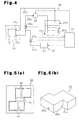
Fig. 4 is a schematic diagram showing a heating medium supply unit and cooling medium supply unit connected to the soldering apparatus ofFig. 3 ; -
Fig. 5(a) is a plan view showing a jig used for soldering; -
Fig. 5(b) is a perspective view showing a weight used for soldering; and -
Fig. 6 is a schematic cross-sectional view of a soldering apparatus according to a second embodiment of the present invention. - A first embodiment of the present invention will now be described with reference to
Figs. 1 to 5 . - As shown in
Fig. 1 , a semiconductor module (semiconductor device) 10 includes acircuit board 11 and a plurality ofsemiconductor elements 12, which serve as electronic components. The plurality ofsemiconductor elements 12 are soldered and bonded to thecircuit board 11. Thecircuit board 11 includes a plurality of (six in the present embodiment)ceramic substrates 14, which serve as insulation substrate.Metal circuits 13 are arranged on the surface of eachceramic substrate 14. Foursemiconductor elements 12 are soldered to eachceramic substrate 14. A total of twenty-foursemiconductor elements 12 are laid out on thesemiconductor module 10. - As shown in
Fig. 2 , thecircuit board 11 includes theceramic substrates 14 and ametal heat sink 15, which is fixed to theceramic substrates 14 with ametal plate 16 arranged therebetween. That is, thecircuit board 11 is a cooling circuit board. Theheat sink 15 has arefrigerant passage 15a, through which refrigerant flows. As shown inFig. 1 , therefrigerant passage 15a includes aninlet 15b and anoutlet 15c. Theinlet 15b and theoutlet 15c are formed to be connectable to a cooling medium circuit (for example, one installed in a vehicle). Theheat sink 15 is formed from an aluminum metal, copper, or the like. An aluminum metal refers to aluminum or an aluminum alloy. Themetal plate 16, which functions as a bonding layer for bonding theceramic substrates 14 and theheat sink 15, is formed from, for example, aluminum or copper. - The
metal circuits 13 are formed from, for example, aluminum, copper, or the like. Theceramic substrates 14 are formed from, for example, aluminum nitride, alumina, silicon nitride, or the like. Thesemiconductor elements 12 are bonded (soldered) to themetal circuits 13. More specifically, themetal circuits 13 serve as bonding portions for bonding thesemiconductor elements 12 to thecircuit board 11. InFig. 2 , character H indicates a soldering layer. Thesemiconductor elements 12 may be, for example, IGBTs (Insulated Gate Bipolar Transistors) or diodes. - A method for manufacturing the
semiconductor module 10 will now be described. -
Fig. 3 schematically shows the structure of a soldering apparatus. The soldering apparatus HK is used to solder thesemiconductor elements 12 to themetal circuits 13, which are arranged on thecircuit board 11. Further, the soldering apparatus HK of this embodiment is used to solder thesemiconductor elements 12 on thecircuit board 11, which includes the plurality of (six)ceramic substrates 14 arranged on theheat sink 15. - The soldering apparatus HK includes a sealable container (chamber) 17. The
container 17 includes amain body 18 and acover body 19. Themain body 18 is box-shaped and has anopening 18a. Thecover body 19 opens and closes theopening 18a of themain body 18. Asupport base 20, which functions as a support for positioning and supporting thesemiconductor module 10, is arranged on themain body 18. A packing 21, which comes into close contact with thecover body 19, is arranged in the open end of themain body 18. Thecover body 19 is large enough to close theopening 18a of themain body 18. Attachment of thecover body 19 to themain body 18 defines a sealed space S in thecontainer 17. - A reducing
gas supply unit 23, which supplies reducing gas (hydrogen in this embodiment) into thecontainer 17, is connected to themain body 18. The reducinggas supply unit 23 includes apipe 23a, avalve 23b arranged in thepipe 23a, and ahydrogen tank 23c. An inertgas supply unit 24, which supplies inert gas (nitrogen in the present embodiment) into thecontainer 17, is connected to themain body 18. The inertgas supply unit 24 includes a pipe 24a, avalve 24b arranged in the pipe 24a, and anitrogen tank 24c. Agas discharge unit 25, which discharges gas filled in thecontainer 17 to the outside, is connected to themain body 18. Thegas discharge unit 25 includes apipe 25a, avalve 25b arranged in thepipe 25a, and avacuum pump 25c. The soldering apparatus HK is configured so that it can adjust the pressure in the sealed space S with the reducinggas supply unit 23, the inertgas supply unit 24, and thegas discharge unit 25. The pressure adjustment pressurizes or depressurizes the sealed space S. Electromagnetic valves are used as thevalves - A heating
medium supplying unit 26, which supplies a heating medium heated in therefrigerant passage 15a of thecircuit board 11 when heating the solder, is connected to themain body 18. Further, a coolingmedium supplying unit 27, which supplies a cooling medium to therefrigerant passage 15a after stopping the heating of the solder, is connected to themain body 18. - Referring to
Fig. 4 , the heatingmedium supplying unit 26 includes a heatingmedium heating unit 26a arranged outside themain body 18. The heatingmedium heating unit 26a includes aheater 26b. In a state in which thecircuit board 11 is supported by thesupport base 20, the heatingmedium heating unit 26a is connected to therefrigerant passage 15a by apipe 28a and thepipe 28c. One end of thepipe 28a is connectable to theinlet 15b of therefrigerant passage 15a, and one end of thepipe 28c is connectable to theoutlet 15c of therefrigerant passage 15a. Apump 29 and avalve 28b, which is located downstream to thepump 29, are arranged in thepipe 28a. When thepump 29 is driven, a heating medium circulates through the heatingmedium heating unit 26a, thepipe 28a, therefrigerant passage 15a, and thepipe 28c. In this embodiment, a liquid such as polyphenylether may be used as the heating medium. - Further, a cooling
medium supplying unit 27 includes acompressor 30, apipe 27a, and avalve 27b arranged in thepipe 27a. Thepipe 27a has one end connected to thecompressor 30 and another end connected to thepipe 28a downstream to thevalve 28b. Electromagnetic valves are used as thevalves - A
controller 31 controls thevalves heater 26b, thepump 29, and thecompressor 30. Thecontroller 31 receives a detection signal of a pressure sensor (not shown), which detects the pressure in thecontainer 17, and a detection signal of atemperature sensor 26c, which detects the temperature of a heating medium heated by the heatingmedium heating unit 26a. Thecontroller 31 controls theheater 26b based on the detection signal of thetemperature sensor 26c. Thecontroller 31 functions as a control unit for controlling the temperature of the heating medium supplied to therefrigerant passage 15a. -
Fig. 5(a) shows ajig 32 used for soldering.Fig. 5(b) shows aweight 35. Thejig 32 is flat and has the same size as theceramic substrates 14 of thecircuit board 11. Thejig 32 is formed from a material such as graphite or ceramics. As shown inFig. 3 , during soldering, thejig 32 is used to positionsolder sheets 33, thesemiconductor elements 12, and theweight 35 on theceramic substrate 14. Thejig 32 has a plurality of positioning holes 34. Theholes 34 are formed in thejig 32 at positions corresponding to portions (bonding portions) of theceramic substrate 14 to which thesemiconductor elements 12 are bonded. Eachhole 34 has dimensions corresponding to the size of thecorresponding semiconductor element 12. In this embodiment, a plurality of (four)semiconductor elements 12 are bonded to theceramic substrate 14. Thus, a plurality of (four)holes 34 are formed in thejig 32. - The
weight 35 is large enough to come in contact with the upper surfaces of the four semiconductor elements 12 (non-bonding surfaces) positioned by thejig 32 during soldering. Theweight 35 presses the four semiconductor elements toward thecircuit board 11 with its weight and spreads the melted solder between bonding surfaces of thesemiconductor elements 12 and a bonding portion of thecircuit board 11. Theweight 35 has a side that comes into contact with the foursemiconductor elements 12 during soldering and defines a pressing surface shaped in correspondence with the layout of the foursemiconductor elements 12. In the present embodiment, the pressing surface of theweight 35 is divided into fourpressing surfaces 35a. Thepressing surfaces 35a are shaped so that they are insertable into the fourholes 34 of thejig 32 in a manner enabling contact with thecorresponding semiconductor elements 12.Fig. 5(a) indicates the contour of thepressing surfaces 35a of theweight 35 with a double-dashed line and shows the positional relationship between thejig 32 and theweight 35 when theweight 35 is inserted into theholes 34 of thejig 32. - A method for soldering the
semiconductor elements 12 to thecircuit board 11 with the soldering apparatus HK will now be described. The soldering is one of the processes that are performed when manufacturing thesemiconductor module 10. Before performing soldering with the soldering apparatus HK, a plurality of (six)ceramic substrates 14, each including ametal circuit 13, are bonded to asingle heat sink 15 to form an object (hereafter referred to as the "soldering subject." The soldering subject corresponds to thesemiconductor module 10 shown inFig. 1 less thesemiconductor elements 12. - When performing soldering, the
cover body 19 is first removed from themain body 18 to open theopening 18a. The soldering subject is then placed and positioned on thesupport base 20 of themain body 18. Next, ajig 32 is arranged on eachceramic substrate 14 of the soldering subject.Solder sheets 33 andsemiconductor elements 12 are arranged in theholes 34 of thejig 32. In this state, thesolder sheets 33, thesemiconductor elements 12, and theweight 35 are arranged in an overlapping manner from themetal circuit 13 on eachceramic substrate 14. Further, in a state in which eachweight 35 extends over foursemiconductor elements 12, thepressing surfaces 35a of theweight 35 comes into contact with the non-bonding surfaces of thesemiconductor elements 12. In this state, theweight 35 is arranged so that its weight presses thesemiconductor elements 12. - Next, the
cover body 19 is attached to themain body 18 to close theopening 18a and form the sealed space S in thecontainer 17. Then, a control signal of thecontroller 31 operates thegas discharge unit 25 to depressurize thecontainer 17. Further, the inertgas supply unit 24 is operated to supply nitrogen into thecontainer 17 and fill the sealed space S with inert gas. After repeating the depressurizing and the supplying of nitrogen a few times, the reducinggas supply unit 23 is operated to supply hydrogen into thecontainer 17 and create a reducing gas atmosphere in the sealed space S. - Then, the
controller 31 controls and switches thevalve 27b to a closed state and thevalve 28b to an open state. Further, thecontroller 31 controls and drives thepump 29. As a result, the heating medium heated by theheater 26b in the heatingmedium heating unit 26a is supplied via thepipe 28a and the like to therefrigerant passage 15a by the action of thepump 29. The heat of the heated heating medium is transmitted to thesolder sheets 33 via theheat sink 15, theceramic substrates 14, and themetal circuits 13. Thesolder sheets 33 then melt as the temperature becomes greater than or equal to its melting point. Thecontroller 31 controls theheater 26b so that the temperature of the heating medium in the heatingmedium heating unit 26a reaches a predetermined temperature higher than the melting point of thesolder sheets 33. When thepump 29 is driven, the heating medium is heated to a temperature higher than the melting point of thesolder sheets 33, and the high-temperature heating medium is supplied to therefrigerant passage 15a. The heating medium supplied to therefrigerant passage 15a returns to the heatingmedium heating unit 26a via theoutlet 15c and thepipe 28c to be heated by theheater 26b and used repetitively. - The
semiconductor elements 12 are pressed toward thecircuit board 11 by theweight 35 and thus are not moved by the surface tension of the melted solder. When thesolder sheets 33 completely melt, thepump 29 is deactivated and thevalve 28b is closed to stop the supply of heating medium to therefrigerant passage 15a. This stops the heating of the solder. Experiments are conducted beforehand to obtain the required time for thesolder sheets 33 to completely melt from when the supply of the heating medium is started. The required time is set beforehand in thecontroller 31. Thecontroller 31 controls thepump 29 and the like so that the supply of the heating medium is stopped as the required time elapses from when the supply of the heating medium is started. This eliminates the need to check whether thesolder sheets 33 have completely melted. - The
heater 26b is controlled based on the detection result of thetemperature sensor 26c arranged in the heatingmedium heating unit 26a. The atmosphere in thecontainer 17, that is, the atmosphere of the sealed space S, is adjusted in accordance with the progress in the soldering operation. In other words, the pressure in thecontainer 17 is adjusted in accordance with the progress in the soldering operation. - After stopping the supply of the heated heating medium to the
refrigerant passage 15a, thevalve 27b opens to supply therefrigerant passage 15a with compressed air as a cooling medium from thecompressor 30. As a result, the heating medium remaining in thepipe 28a at a portion downstream from the portion connected to thepipe 27a is recovered in the heatingmedium heating unit 26a. The compressed air supplied to therefrigerant passage 15a cools theheat sink 15 and members arranged on theheat sink 15. The compressed air is then sent to the heatingmedium heating unit 26a via theoutlet 15c and thepipe 28c and discharged out of a discharge port (not shown) arranged in the heatingmedium heating unit 26a. Consequently, the melted solder solidifies as it cools down to a temperature below the melting point and bonds themetal circuit 13 and thesemiconductor elements 12. This ends the soldering operation and completes thesemiconductor module 10. - After the temperature of the solder is lowered to a predetermined temperature, the
valve 27b is closed to stop the supply of the cooling medium to therefrigerant passage 15a. Then, thecover body 19 is removed from themain body 18, and theweights 35 andjigs 32 are removed from thesemiconductor module 10. One end of thepipe 28a is removed from theinlet 15b, and one end of thepipe 28c is removed from theoutlet 15c. Then, thesemiconductor module 10 is taken out of thecontainer 17. Experiments are conducted beforehand to obtain the required time for the temperature of the solder to decrease to a predetermined temperature from when the supply of the cooling medium is started. The required time is set beforehand in thecontroller 31. Thecontroller 31 controls thevalve 27b and the like so that the supply of the cooling medium is stopped as the required time elapses from when the supply of the cooling medium is started. This eliminates the need to check whether the solder temperature has decreased to the predetermined temperature. - This embodiment has the advantages described below.
- (1) When soldering the
circuit board 11 and thesemiconductor elements 12, thecircuit board 11 is used as a cooling circuit board. The cooling circuit board includes the ceramic substrates 14 (insulation substrates), the front surfaces on which themetal circuits 13 are arranged, and themetal heat sink 15, which is fixed to the rear surfaces of theceramic substrates 14. In a state in which solder is arranged between themetal circuits 13 and thesemiconductor elements 12, the heated heating medium is sent into therefrigerant passage 15a to heat and melt the solder. The heat of the heating medium is transmitted to the solder via themetal heat sink 15, which has superior heat conductance. Afterwards, the heating of the solder is stopped and the melted solder is cooled to complete the soldering. Accordingly, unlike when entirely heating thecontainer 17 or heating thesemiconductor elements 12 from above with a heater, that is, unlike when transmitting heat to the solder via a gas of which heat conductance is lower than theheat sink 15 by at least a two digit value, the heat of the heating medium in the present embodiment is transmitted to the solder without passing through a gas. Thus, the solder is efficiently heated. - (2) After the heating of solder is stopped, a cooling medium is sent into the
refrigerant passage 15a to cool the circuit board 11 (cooling circuit board) and the solder. That is, therefrigerant passage 15a of theheat sink 15 is used as a passage for the cooling medium and not just as a passage for the heating medium. Accordingly, the solder is efficiently cooled, and the time required to cool the semiconductor elements to a predetermined temperature is shortened. - (3) The soldering is performed in the
sealable container 17. Thus, in comparison with when performing soldering in a state open to the outer side, the heat of the heating medium does not easily escape and the solder is further efficiently heated. - (4) The
weight 35 is arranged on and extends over a plurality ofsemiconductor elements 12 that are not laid out straight. Further, the solder is heated and melted in a state in which theweight 35 presses thesemiconductor elements 12 toward thecircuit board 11. Accordingly, when the solder melts, theweight 35 presses thesemiconductor elements 12 toward the bonding surface in a horizontal state or a generally horizontal state. Thus, the melted solder between thesemiconductor elements 12 and themetal circuits 13 spreads out entirely on the surfaces of thesemiconductor elements 12 facing toward themetal circuits 13. When the solder cools to a temperature that is lower than or equal to its melting point, the solder solidifies at the bonding portions with a uniform thickness. - (5) The
weight 35 includes the plurality ofpressing surfaces 35a respectively shaped in correspondence with the contours of thesemiconductor elements 12. Further, theweight 35 presses the plurality ofsemiconductor elements 12 with all of thepressing surfaces 35a. Accordingly, pressing forces applied to thesemiconductor elements 12 are uniformed so that differences in the solder thickness at the bonding portions are decreased. - (6) The
semiconductor module 10 includes thecircuit board 11, which serves as a cooling circuit board. Thecircuit board 11 is formed by fixing one or moreceramic substrates 14, having surfaces on which themetal circuits 13 are arranged, to themetal heat sink 15, which includes therefrigerant passage 15a. The solder spreads out entirely on the surfaces of thesemiconductor elements 12 facing towards themetal circuits 13 and solidifies with a uniform thickness. Accordingly, in thesemiconductor module 10, the solder functions to relax stress by absorbing differences in the coefficient of linear expansion between thesemiconductor elements 12 and themetal circuits 13. This prevents variations in the fatigue life of the bonding portions. - (7) A liquid is used as the heating medium, and a gas is used as the cooling medium. Accordingly, by supplying the cooling medium to the
refrigerant passage 15a, the heating medium remaining in the refrigerant passage is easily recovered in the heatingmedium heating unit 26a without mixing with the cooling medium. - (8) Compressed air is used as the cooling medium. This lowers costs in comparison to when other gases are used.
A second embodiment of the present invention will now be described with reference toFig. 6 . The second embodiment differs from the first embodiment in that in addition to the heatingmedium supplying unit 26 that supplies therefrigerant passage 15a with a heating medium for heating the solder on the circuit board, a heating device that does not use the heat of a heating medium to heat the solder is further employed. Otherwise, the structure of the second embodiment is basically the same as the first embodiment. Similar parts will not be described in detail.
The soldering apparatus HK includesweights 35 and high frequency heating coils 36. Theweights 35 are placed onsemiconductor elements 12 and formed from a material enabling induction heating. The high frequency heating coils 36 can heat theweights 35 through high frequency induction. Theweights 35 and the highfrequency heating coil 36 functions as a heating device. Thecover body 19 includes aportion 22 facing toward the sealed space S. Theportion 22 is formed from an electrical insulating material that allows passage of magnetic lines of flux (magnetic flux). In the present embodiment, glass is used as the electrical insulating material. Theportion 22 of thecover body 19 is formed by aglass plate 22.
High frequency heating coils 36 are arranged at an upper part of the soldering apparatus HK, specifically, above thecover body 19. The present embodiment includes six high frequency heating coils 36. As shown inFig. 6 , the high frequency heating coils 36 are arranged to face sixceramic substrates 14, respectively. In this embodiment, when viewed from above, each highfrequency heating coil 36 is large enough to cover a singleceramic substrate 14 and larger than the contour of the upper surface of theweight 35. Each highfrequency heating coil 36 is spirally wound within a single plane so as to form a substantially quadrangular plate as a whole. Each highfrequency heating coil 36 is arranged to face thecover body 19, specifically to face thegrass plate 22. The high frequency heating coils 36 are electrically connected to ahigh frequency generator 37 of the soldering apparatus HK. The output of thehigh frequency generator 37 is controlled based on the measurement result of atemperature sensor 38, which is arranged in thecontainer 17. Each highfrequency heating coil 36 has acoolant passage 36a, through which coolant flows. The high frequency heating coils 36 are connected to acoolant tank 39 of the soldering apparatus HK.
Theweight 35 is formed from a material that can be heated through electromagnetic induction. More specifically, theweight 35 is formed from a material that generates heat due to its electric resistance when current is generated as changes occur in the magnetic flux passing through theweight 35. In this embodiment, theweights 35 are formed from stainless steel.
A method for soldering thesemiconductor elements 12 with the soldering apparatus HK will now be described. The soldering is one of the processes that are performed when manufacturing thesemiconductor module 10.
In the same manner as in the first embodiment, when performing soldering with the soldering apparatus HK of this embodiment, thejigs 32 are placed on theceramic substrates 14 of the soldering subject supported on thesupport base 20 of themain body 18. In this state, thesolder sheets 33 and thesemiconductor elements 12 are arranged in the holes of thejigs 32, and theweights 35 are arranged on thesemiconductor elements 12.
Then, thecover body 19 is attached to themain body 18 to close theopening 18a and form a sealed space S in thecontainer 17. In a state in which thecircuit board 11, thesolder sheets 33, thesemiconductor elements 12, and theweights 35 are accommodated in the sealed space S, the high frequency heating coils 36 are arranged above the correspondingweights 35. Theglass plate 22, which is attached to thecover body 19, is located between the high frequency heating coils 36 and theweights 35. In this embodiment, each highfrequency heating coil 36 is formed and arranged so that when viewed from above, the highfrequency heating coil 36 extends out of a region defined by the contour of the upper surface of theweight 35. In this embodiment, a large amount of magnetic flux is generated near the central part of the highfrequency heating coil 36, which is spirally wound. Thus, it is preferable that theweight 35 be arranged near the central part of the highfrequency heating coil 36.
Then, a control signal of thecontroller 31 operates thegas discharge unit 25 to depressurize thecontainer 17. Further, the inertgas supply unit 24 is operated to supply nitrogen into thecontainer 17 and fill the sealed space S with inert gas. After repeating the depressurizing and the supplying of nitrogen a few times, the reducinggas supply unit 23 is operated to supply hydrogen into thecontainer 17 and create a reducing gas atmosphere in the sealed space S.
Next, in the same manner as in the first embodiment, thecontroller 31 controls and switches thevalve 27b to a closed state and thevalve 28b to an open state. Further, thepump 29 is driven so that the heating medium heated by theheater 26b in the heatingmedium heating unit 26a is supplied via thepipe 28a and the like to therefrigerant passage 15a by the action of thepump 29. The heat of the heated heating medium is transmitted to thesolder sheets 33 via theheat sink 15, theceramic substrates 14, and themetal circuits 13.
Then, thehigh frequency generator 37 is operated to generate high frequency current that flows to each highfrequency heating coil 36. As a result, the highfrequency heating coil 36 generates high frequency magnetic flux, which passes through the correspondingweight 35. The passage of the magnetic flux generates eddy current in theweight 35. As a result, theweight 35, which is arranged in the magnetic flux of the highfrequency heating coil 36, generates heat through electromagnetic induction. The heat is transmitted from thepressing surfaces 35a of theweight 35 to thecorresponding semiconductor elements 12. The heat generated in theweight 35 is transmitted to thesolder sheets 33 in a concentrated manner through thepressing surfaces 35a of theweight 35 and thesemiconductor elements 12. This heats thesolder sheets 33.
As a result, the heat of the heating medium flowing through therefrigerant passage 15a and the heat generated at theweights 35 through induction heating by the high frequency heating coils 36 both heat the solder (solder sheets 33). This heats the solder from both of the upper and lower sides. Thus, the heating is more quickly and efficiently performed.
When thesolder sheets 33 completely melt, thepump 29 is deactivated and thevalve 28b is closed to stop the supply of heating medium to therefrigerant passage 15a. Further, thehigh frequency generator 37 is deactivated to stop heating the solder. Experiments are conducted beforehand to obtain the required time for thesolder sheets 33 to completely melt from when the supply of the heating medium is started and when the supply of high frequency current to the high frequency heating coils 36 is started. The required time is set beforehand in thecontroller 31. Thecontroller 31 controls thepump 29, the high frequency heating coils 36, and the like so that the supply of the heating medium and the supply of the high frequency current is stopped as the required time elapses from when the supply of the heating medium and the high frequency current is started. This eliminates the need to check whether thesolder sheets 33 have completely melted.
In the same manner as in the first embodiment, compressed air as a cooling medium is then supplied to therefrigerant passage 15a. Further, thecontroller 31 controls thevalve 27b and the like to stop supplying the cooling medium when a predetermined time, which is set beforehand, elapses from when the supply of the cooling medium is started.
In addition to advantages (1) to (8) of the first embodiment, this embodiment has the advantages described below. - (9) The solder (solder sheet 33) is heated by the heat of the heated heating medium flowing through the
refrigerant passage 15a and the heat of the further heating device. This heats the solder within a shorter period of time. - (10) The further heating device generates heat by performing high frequency induction with the
weights 35, which are placed on thesemiconductor elements 12 and formed from a material enabling induction heating. The heat is transmitted from theweights 35 via thesemiconductor elements 12 to the solder. Accordingly, in comparison with a heater (electric heater) used in a typical reflow furnace, heat is transmitted in a concentrated manner to the solder. Thus, the solder is efficiently heated. More specifically, the heating medium supplied to therefrigerant passage 15a uniformly heats theentire heat sink 15. Further, theweights 35 heated by induction heating locally heats vicinity of the solder. As a result, the advantages of the two heating schemes are combined thereby enabling satisfactory temperature control. - (11) The heated heating medium and the further heating device heat the solder. Thus, the solder can be melted without heating the heating medium to a temperature that is higher than the melting point of the solder. In other words, the heated heating medium heats the solder in a supplemental manner, while the further heating device heats the solder to a temperature that is higher than the melting point. This increases freedom in the selection of the material used as the heating medium.
- (12) When performing soldering on the
circuit board 11, which includes the plurality ofceramic substrates 14, one highfrequency heating coil 36 is arranged on each ceramic substrate 14 (weight 35), and theweight 35 on theceramic substrate 14 is heated. This increases efficiency in comparison with when one highfrequency heating coil 36 heats a plurality of theweights 35, which are respectively arranged on theceramic substrates 14. - (13) The high frequency heating coils 36 is arranged outside the
container 17 and not inside thecontainer 17. This enables the volume of thecontainer 17 to be minimized and enables thecontainer 17 to be reduced in size. Further, the atmosphere adjustment mainly includes the discharge of air from the container 17 (depressurization), the supply and discharge of inert gas (nitrogen gas etc.), and the supply and discharge of reducing gas (hydrogen etc.). Thus, reduction in the volume of thecontainer 17 would, for example, shorten the time required for discharging air and decreases the consumption of energy required for discharging air (e.g., the energy required to operate thevacuum pump 25c). Further, the time required for supplying or discharging inert gas or reducing gas may be shortened, the energy required for supplying or discharging inert gas or reducing gas may be decreased, and the consumption of the supplied gas may be lowered. - The embodiments are not limited to those described above and may be modified as described below.
- The heating medium supplied to the
refrigerant passage 15a may be a gas. For example, hydrogen gas, nitrogen gas, or the like may be used as the gas. When using a gas as the heating medium, it is preferable that hydrogen gas be used since it has a larger heat conductance and larger specific heat than other gases. The heating medium and the cooling medium may both be hydrogen gas. However, this would increase the amount of the used hydrogen gas. Thus, the use of a gas other than hydrogen gas as the cooling medium, for example, nitrogen gas, would lower costs. - When using a gas as the heating medium, the heat generated when the heating medium is compressed by a compressor and the heat generated when the heater heats the heating medium may both be used. In this case, the compressor functions as the
pump 29. - The liquid heating medium is not limited to polyphenylether. For example, LLC (long-life coolant) may be used as the heating medium. In this case, it is difficult to heat the heating medium to a temperature higher than the melting point of the solder. Thus, it is preferred that the structure of the second embodiment be employed since a further heating device is used.
- A liquid may be used as the cooling medium.
- When using a cooling medium, a heat exchanger may be arranged in the
pipe 27a, and a cooling medium cooled by the heat exchanger may be supplied to therefrigerant passage 15a. This enables the solder to be cooled within a shorter time. Further, a cooling medium that is not cooled may be initially supplied to therefrigerant passage 15a, and then the cooled cooling medium may be supplied to therefrigerant passage 15a. - The further heating device is not limited to a structure including the
weights 35, which can undergo induction heating, and the high frequency heating coils 36. For example, an electric heater for heating the solder or a device for emitting a laser beam may be arranged in thecontainer 17. - The electronic components soldered to the
metal circuit 13 of thecircuit board 11 are not limited to thesemiconductor elements 12. For example, the electronic components may be chip resistors or chip capacitors. - The
weights 35 do not all have to be of the same size and shape. For example, the plurality ofsemiconductor elements 12 may be divided into a plurality of groups, and theweights 35 may be shaped in correspondence with the layout of thesemiconductor elements 12 in each group. - The
pressing surfaces 35a of eachweight 35 does not need to have a size enabling contact with the entire non-bonding surfaces of thecorresponding semiconductor elements 12 and may be larger or smaller. - The
jig 32 is not limited to a structure that functions to position thesolder sheets 33, thesemiconductor elements 12, and theweights 35 and may have a structure that functions to position only thesolder sheets 33 and thesemiconductor elements 12. - In a structure in which the solder is melted with the heat generated by the
weights 35 through induction heating, theweights 35 do not have to be formed from stainless steel. Theweights 35 may be formed from any material suitable for induction heating. For example, theweights 35 may be formed from iron or graphite instead of stainless steel or may be formed from two conductive materials having different thermal conductivity coefficients. - Instead of arranging the
solder sheets 33 at locations corresponding to bonding portions on themetal circuit 13, a solder paste may be applied at the locations corresponding to the bonding portions. - The
cover body 19 may be configured so as not detachable to themain body 18 and may be connected to themain body 18 so that thecover body 19 can open and close themain body 18. - It is preferable that at least a portion of the
cover body 19 facing toward the high frequency heating coils 28 be formed from an electrically insulative material. Instead of glass, this portion may be formed from ceramics or a resin. Further, thecover body 19 may entirely be formed from the same electrically insulative material. - When the strength of the
cover body 19 must be increased in accordance with the pressure difference between the inside and outside of thecontainer 17, thecover body 19 may be formed from a complex material (GFRP (glass fiber reinforced plastics)) of glass fiber and resin. Further, thecover body 19 may be formed from metal. The metal is preferably a non-magnetic metal. If magnetic metal is used as the material for thecover body 19, it is preferred that a metal having a higher electrical resistivity than theweight 35 be used. Thecover body 19 may be formed from complex material of metal and an insulative material. An electromagnetic steel plate etc. of ferromagnetic body may be used immediately above theweight 35 to effectively guide magnetic flux to theweight 35. - Each high
frequency heating coil 36 may be arranged above the plurality ofweights 35 so as to extend over the plurality ofweights 35. In this case, the supply path of the high frequency current and the supply path of the cooling water to the highfrequency heating coil 36 may be shortened, and the structure of the soldering device HK may be further simplified. - The
container 17 may be movable along a production line, and the highfrequency heating coil 36 may be arranged along the movement path of theweights 35, which move together with thecontainer 17. In this case, the highfrequency heating coil 36 may be shaped to extend along the movement path or may be arranged at plural locations along the movement path. In such a structure, thecontainer 17 can be heated as it moves. - The high frequency heating coils 36 may be arranged so as to face toward the side surfaces of the
weights 35. - The high frequency heating coils 28 may be arranged in the container 17 (sealed space S).
- During soldering, instead of pressing the
semiconductor elements 12 with the weight of theweights 35, a biasing member such as a spring may be used to press thesemiconductor elements 12. - The components soldered to the
circuit board 11 is not limited to chip components and may be lead components including leads. - Soldering does not have to be performed in the
sealable container 17. For example, soldering may be performed in a container having a loading port, through which thecircuit board 11 is loaded in a state placed on a conveying device such as a belt conveyor, and an unloading port, from which thecircuit board 11 is unloaded. Further, soldering may be performed without the container. That is, soldering may be performed in a state where no enclosing member, which encloses the location of the soldering, is provided. - When soldering electronic components onto the
circuit board 11, which includes theheat sink 15, the solder may be heated by the further heating device without supplying a heating medium to therefrigerant passage 15a, and theheat sink 15 may be used only for cooling.
Claims (21)
- A soldering method for soldering an electronic component onto a circuit board, the method comprising:using as the circuit board a cooling circuit board including an insulation substrate and a metal heat sink, the insulation substrate having a front surface with a metal circuit and a rear surface to which the heat sink is fixed, and the heat sink having a refrigerant passage;arranging the electronic component on the metal circuit with solder in between; andsupplying a heated heating medium to the refrigerant passage when heating and melting the solder.
- The soldering method according to claim 1, further comprising:supplying a cooling medium to the refrigerant passage to cool the cooling circuit board and the solder after stopping the heating of the solder.
- The soldering method according to claim 2, further comprising:using a liquid as the heating medium; andusing a gas as the cooling medium.
- The soldering method according to any one of claims 1 to 3, further comprising:retaining the cooling circuit board in a sealable container; andheating the solder with a heating device while supplying the refrigerant passage with the heated heating medium to melt the solder in a state in which the cooling circuit board is retained in the container.
- The heating method according to claim 4, wherein said heating the solder with a heating device includes performing high frequency induction to generate heat with a weight formed from a material enabling induction heating and placed on the electronic component, and transmitting the heat of the weight to the solder through the electronic component.
- The soldering method according to any one of claims 1 to 5, further comprising:using a heat sink made of aluminum or copper.
- A soldering method for soldering an electronic component onto a circuit board, the method comprising:using as the circuit board a cooling circuit board including an insulation substrate and a metal heat sink, the insulation substrate having a front surface with a metal circuit and a rear surface to which the heat sink is fixed, and the heat sink having a refrigerant passage;arranging the electronic component on the metal circuit with solder in between;heating and melting the solder; andsupplying a cooling medium to the refrigerant passage to cool the cooling circuit board and solder after stopping the heating of the solder.
- A method for manufacturing a semiconductor module formed by soldering an electronic component onto a circuit board, the method comprising:using as the circuit board a cooling circuit board including an insulation substrate and a metal heat sink, the insulation substrate having a front surface with a metal circuit and a rear surface to which the heat sink is fixed, and the heat sink having a refrigerant passage;arranging the electronic component on the metal circuit with solder in between; andsupplying a heated heating medium to the refrigerant passage when heating and melting the solder.
- The manufacturing method according to claim 8, further comprising:supplying a cooling medium to the refrigerant passage to cool the cooling circuit board and the solder after stopping the heating of the solder.
- The manufacturing method according to claim 9, further comprising:using a liquid as the heating medium; andusing a gas as the cooling medium.
- The manufacturing method according to any one of claims 8 to 10, further comprising:retaining the cooling circuit board in a sealable container; andheating the solder with a heating device while supplying the refrigerant passage with the heated heating medium to melt the solder in a state in which the cooling circuit board is retained in the container.
- The manufacturing method according to claim 11, wherein said heating the solder with a heating device includes performing high frequency induction to generate heat with a weight formed from a material enabling induction heating and placed on the electronic component, and transmitting the heat of the weight to the solder through the electronic component.
- The manufacturing method according to any one of claims 8 to 12, further comprising:using a heat sink made of aluminum or copper.
- A method for manufacturing a semiconductor module formed by soldering an electronic component onto a circuit board, the method comprising:using as the circuit board a cooling circuit board including an insulation substrate and a metal heat sink, the insulation substrate having a front surface with a metal circuit and a rear surface to which the heat sink is fixed, and the heat sink having a refrigerant passage;arranging the electronic component on the metal circuit with solder in between;heating and melting the solder; andsupplying a cooling medium to the refrigerant passage to cool the cooling circuit board and solder after stopping the heating of the solder.
- A soldering apparatus for soldering an electronic component onto a circuit board, the soldering apparatus comprising:a support capable of supporting the circuit board, wherein the circuit board is a cooling circuit board including an insulation substrate and a metal heat sink, the insulation substrate having a front surface with a metal circuit and a rear surface to which the heat sink is fixed, and the heat sink having a refrigerant passage, with the refrigerant passage including an inlet and an outlet;a heating medium supply unit capable of supplying a heating medium to the refrigerant passage, with the heating medium supply unit including a pipe connectable to the inlet and the outlet in a state in which the cooling circuit board is supported by the support; anda control unit for controlling temperature of the heating medium supplied to the refrigerant passage.
- The soldering apparatus according to claim 15, further comprising:a sealable container for retaining the cooling circuit board, with the support being arranged in the container.
- The soldering apparatus according to claim 15 or 16, further comprising:a heating device capable of heating solder on the cooling circuit board supported by the support.
- The soldering apparatus according to claim 17, wherein the heating device includes a weight formed from a material enabling induction heating and placeable on the electronic component, and a high frequency heating coil capable of generating heat with the weight through high frequency induction.
- The soldering apparatus according to any one of claims 15 to 18, further comprising:a cooling medium supply unit capable of supplying a cooling medium to the refrigerant passage in a state in which the cooling circuit board is supported by the support.
- The soldering apparatus according to claim 19, wherein the heating medium is a liquid, and the cooling medium is a gas.
- The soldering apparatus according to any one of claims 15 to 20, wherein the heat sink is made of aluminum or copper.
Applications Claiming Priority (2)
| Application Number | Priority Date | Filing Date | Title |
|---|---|---|---|
| JP2005380354A JP4640170B2 (en) | 2005-12-28 | 2005-12-28 | Soldering method, semiconductor module manufacturing method, and soldering apparatus |
| PCT/JP2006/325944 WO2007074835A1 (en) | 2005-12-28 | 2006-12-26 | Soldering method, semiconductor module manufacturing method and soldering apparatus |
Publications (1)
| Publication Number | Publication Date |
|---|---|
| EP1968366A1 true EP1968366A1 (en) | 2008-09-10 |
Family
ID=38218056
Family Applications (1)
| Application Number | Title | Priority Date | Filing Date |
|---|---|---|---|
| EP06843328A Withdrawn EP1968366A1 (en) | 2005-12-28 | 2006-12-26 | Soldering method, semiconductor module manufacturing method and soldering apparatus |
Country Status (6)
| Country | Link |
|---|---|
| US (1) | US20090184152A1 (en) |
| EP (1) | EP1968366A1 (en) |
| JP (1) | JP4640170B2 (en) |
| KR (1) | KR100996396B1 (en) |
| CN (1) | CN101352110A (en) |
| WO (1) | WO2007074835A1 (en) |
Cited By (2)
| Publication number | Priority date | Publication date | Assignee | Title |
|---|---|---|---|---|
| WO2016144714A3 (en) * | 2015-03-06 | 2016-11-03 | Corning Incorporated | Extrusion dies and methods and apparatuses for forming the same |
| DE102021202737A1 (en) | 2021-03-22 | 2022-09-22 | Volkswagen Aktiengesellschaft | Method of connecting a heat-generating component to a cooling device |
Families Citing this family (29)
| Publication number | Priority date | Publication date | Assignee | Title |
|---|---|---|---|---|
| ATE524265T1 (en) * | 2008-03-20 | 2011-09-15 | Komax Holding Ag | SOLDERING DEVICE FOR CONNECTING SOLAR CELLS |
| JP4985536B2 (en) * | 2008-04-25 | 2012-07-25 | 株式会社豊田自動織機 | Positioning jig |
| DE102010016814B3 (en) * | 2010-05-05 | 2011-10-06 | Schott Solar Ag | Method and device for applying solder to a workpiece |
| JP5129848B2 (en) * | 2010-10-18 | 2013-01-30 | 東京エレクトロン株式会社 | Joining apparatus and joining method |
| WO2012070264A1 (en) * | 2010-11-23 | 2012-05-31 | 三菱電機株式会社 | Reflow soldering device and reflow soldering method |
| US8308052B2 (en) * | 2010-11-24 | 2012-11-13 | Taiwan Semiconductor Manufacturing Company, Ltd. | Thermal gradient reflow for forming columnar grain structures for solder bumps |
| TW201233278A (en) * | 2011-01-21 | 2012-08-01 | Power Mate Technology Co Ltd | Method for welding electronic components by high frequency |
| DE102011081606B4 (en) * | 2011-08-26 | 2022-08-04 | Infineon Technologies Ag | Cooling device and soldering system |
| CN202281972U (en) * | 2011-10-13 | 2012-06-20 | 鸿富锦精密工业(深圳)有限公司 | Electronic device and heat dissipation device thereof |
| ES2621481T3 (en) * | 2011-10-25 | 2017-07-04 | L'air Liquide, Societe Anonyme Pour L'etude Et L'exploitation Des Procedes Georges Claude | Method and device for cooling soldered printed circuit boards |
| CN103247555B (en) * | 2012-02-08 | 2016-07-06 | 西安永电电气有限责任公司 | IGBT package tray and IGBT module method for packing |
| JP5793473B2 (en) * | 2012-07-20 | 2015-10-14 | 株式会社新川 | Heater for bonding apparatus and cooling method thereof |
| US9038883B2 (en) * | 2013-09-11 | 2015-05-26 | Princeton Optronics Inc. | VCSEL packaging |
| JP6303623B2 (en) * | 2014-03-07 | 2018-04-04 | 富士電機株式会社 | Semiconductor device, semiconductor device manufacturing method, positioning jig |
| JP6357874B2 (en) * | 2014-05-27 | 2018-07-18 | 富士電機株式会社 | Method for mounting semiconductor module and jig for soldering semiconductor module used in this method |
| JP6327105B2 (en) * | 2014-10-17 | 2018-05-23 | 三菱電機株式会社 | Semiconductor device |
| KR102411595B1 (en) * | 2014-12-26 | 2022-06-20 | 후지 덴키 가부시키가이샤 | Heating and cooling device |
| DE102015106298B4 (en) * | 2015-04-24 | 2017-01-26 | Semikron Elektronik Gmbh & Co. Kg | Device, method and system for inhomogeneous cooling of a flat object |
| KR102429619B1 (en) * | 2015-11-18 | 2022-08-04 | 삼성전자주식회사 | Bonding stage and bonding apparatus comprising the same |
| ITUB20159600A1 (en) * | 2015-12-28 | 2017-06-28 | Velatech S R L | Thermal induction press for the welding of printed circuits and method implemented by this press |
| US10245668B2 (en) * | 2016-10-31 | 2019-04-02 | Kulicke And Soffa Industries, Inc | Fluxing systems, bonding machines including fluxing systems, and methods of operating the same |
| CN106270871A (en) * | 2016-11-01 | 2017-01-04 | 株洲中车时代电气股份有限公司 | The welding method of a kind of semiconductor device and welding system |
| JP6803617B2 (en) * | 2017-12-13 | 2020-12-23 | 株式会社シンアペックス | Reflow device |
| CN108393552B (en) * | 2018-03-02 | 2020-06-12 | 上海航天电子通讯设备研究所 | Electronic product vacuum soaking assembly welding device and welding method thereof |
| CN109175575A (en) * | 2018-09-27 | 2019-01-11 | 君泰创新(北京)科技有限公司 | A kind of lower heating system, series welding device and its method for heating and controlling |
| KR102860020B1 (en) * | 2019-09-06 | 2025-09-12 | 삼성전자주식회사 | Solder bump forming apparatus and forming method for solder bumps |
| US11614289B2 (en) | 2020-01-21 | 2023-03-28 | Dana Canada Corporation | Aluminum heat exchanger with solderable outer surface layer |
| WO2022219796A1 (en) * | 2021-04-16 | 2022-10-20 | 東芝三菱電機産業システム株式会社 | Fluid verification pipe and electric device |
| CN116313946B (en) * | 2023-05-24 | 2023-10-17 | 长鑫存储技术有限公司 | Temperature adjusting system and adjusting method |
Family Cites Families (23)
| Publication number | Priority date | Publication date | Assignee | Title |
|---|---|---|---|---|
| JPS5486457A (en) * | 1977-12-22 | 1979-07-10 | Toshiba Corp | Soldering apparatus |
| JPS55156333A (en) * | 1979-05-25 | 1980-12-05 | Hitachi Ltd | Si chip replacing method |
| JPH0740380B2 (en) * | 1985-11-19 | 1995-05-01 | 株式会社リコー | Magneto-optical recording material |
| US4920574A (en) * | 1985-10-04 | 1990-04-24 | Fujitsu Limited | Cooling system for an electronic circuit device |
| US4879632A (en) * | 1985-10-04 | 1989-11-07 | Fujitsu Limited | Cooling system for an electronic circuit device |
| US5126919A (en) * | 1985-10-04 | 1992-06-30 | Fujitsu Limited | Cooling system for an electronic circuit device |
| JPS62131551A (en) * | 1985-12-03 | 1987-06-13 | Fujitsu Ltd | Heat-sink attaching and detaching method |
| US4747533A (en) | 1986-04-28 | 1988-05-31 | International Business Machines Corporation | Bonding method and apparatus |
| JPH08293668A (en) * | 1995-02-22 | 1996-11-05 | Fuji Electric Co Ltd | Soldering method for printed circuit board and electronic parts |
| JPH08340177A (en) * | 1995-06-13 | 1996-12-24 | Matsushita Electric Ind Co Ltd | Electronic component mounting equipment |
| JPH10178268A (en) * | 1996-10-18 | 1998-06-30 | Fuji Electric Co Ltd | Electronic component soldering method and apparatus |
| DE19645636C1 (en) * | 1996-11-06 | 1998-03-12 | Telefunken Microelectron | Power module for operating electric motor with speed and power control |
| US6211567B1 (en) * | 1998-01-20 | 2001-04-03 | International Rectifier Corp. | Top heatsink for IGBT |
| JP3864282B2 (en) * | 1998-09-22 | 2006-12-27 | 三菱マテリアル株式会社 | Power module substrate, method for manufacturing the same, and semiconductor device using the substrate |
| JP2001148451A (en) * | 1999-03-24 | 2001-05-29 | Mitsubishi Materials Corp | Power module substrate |
| JP2001135758A (en) * | 1999-11-04 | 2001-05-18 | Toyota Autom Loom Works Ltd | Power module heat dissipation structure |
| JP2001257458A (en) * | 2000-03-10 | 2001-09-21 | Fuji Xerox Co Ltd | Member for soldering, and method of soldering |
| JP2001339152A (en) * | 2000-05-29 | 2001-12-07 | Nec Corp | Reflow soldering equipment |
| EP1315205A4 (en) * | 2000-08-09 | 2009-04-01 | Mitsubishi Materials Corp | POWER MODULE MAY COMPRISE A THERMAL DISSIPATOR |
| DE10062108B4 (en) * | 2000-12-13 | 2010-04-15 | Infineon Technologies Ag | Power module with improved transient thermal resistance |
| US6827249B2 (en) * | 2002-09-30 | 2004-12-07 | Newport Corporation | Fluxless tube seal |
| US6992887B2 (en) * | 2003-10-15 | 2006-01-31 | Visteon Global Technologies, Inc. | Liquid cooled semiconductor device |
| JP4945319B2 (en) * | 2007-05-25 | 2012-06-06 | 昭和電工株式会社 | Semiconductor device |
-
2005
- 2005-12-28 JP JP2005380354A patent/JP4640170B2/en not_active Expired - Fee Related
-
2006
- 2006-12-26 US US12/086,990 patent/US20090184152A1/en not_active Abandoned
- 2006-12-26 EP EP06843328A patent/EP1968366A1/en not_active Withdrawn
- 2006-12-26 CN CNA2006800497982A patent/CN101352110A/en active Pending
- 2006-12-26 KR KR1020087015398A patent/KR100996396B1/en not_active Expired - Fee Related
- 2006-12-26 WO PCT/JP2006/325944 patent/WO2007074835A1/en not_active Ceased
Non-Patent Citations (1)
| Title |
|---|
| See references of WO2007074835A1 * |
Cited By (3)
| Publication number | Priority date | Publication date | Assignee | Title |
|---|---|---|---|---|
| WO2016144714A3 (en) * | 2015-03-06 | 2016-11-03 | Corning Incorporated | Extrusion dies and methods and apparatuses for forming the same |
| US11135740B2 (en) | 2015-03-06 | 2021-10-05 | Corning Incorporated | Extrusion dies and methods and apparatuses for forming the same |
| DE102021202737A1 (en) | 2021-03-22 | 2022-09-22 | Volkswagen Aktiengesellschaft | Method of connecting a heat-generating component to a cooling device |
Also Published As
| Publication number | Publication date |
|---|---|
| US20090184152A1 (en) | 2009-07-23 |
| KR100996396B1 (en) | 2010-11-24 |
| WO2007074835A1 (en) | 2007-07-05 |
| CN101352110A (en) | 2009-01-21 |
| KR20080083288A (en) | 2008-09-17 |
| JP2007180458A (en) | 2007-07-12 |
| JP4640170B2 (en) | 2011-03-02 |
Similar Documents
| Publication | Publication Date | Title |
|---|---|---|
| US20090184152A1 (en) | Soldering Method, Semiconductor Module Manufacturing Method, and Soldering Apparatus | |
| KR102411595B1 (en) | Heating and cooling device | |
| KR101004587B1 (en) | Soldering method and manufacturing method of semiconductor module and soldering apparatus | |
| EP1954110A1 (en) | Soldering apparatus and soldering method | |
| WO2007077877A1 (en) | Soldering method, soldering apparatus and method for manufacturing semiconductor device | |
| WO2007083738A1 (en) | Aligning jig, aligning method, method for manufacturing semiconductor module and soldering apparatus | |
| EP1968107A1 (en) | Soldering method and semiconductor module manufacturing method | |
| CN100334701C (en) | Wafer mounting device and method | |
| US20090275174A1 (en) | Soldering Container and Production Method of Semiconductor Device | |
| JP5029279B2 (en) | Soldering apparatus, soldering method, and electronic device manufacturing method | |
| JP2008229709A (en) | Soldering apparatus, soldering method, and electronic device manufacturing method | |
| JP2008147555A (en) | Soldering method, weight and method for manufacturing electronic device | |
| KR101331590B1 (en) | Wafer bonder unsing electromagnetic wave heating | |
| WO2007099873A1 (en) | Method and apparatus for mounting electronic component and semiconductor device manufacturing method | |
| CN115119471A (en) | Method for connecting a heat-generating component to a cooling device | |
| JP2010240670A (en) | Soldering device |
Legal Events
| Date | Code | Title | Description |
|---|---|---|---|
| PUAI | Public reference made under article 153(3) epc to a published international application that has entered the european phase |
Free format text: ORIGINAL CODE: 0009012 |
|
| 17P | Request for examination filed |
Effective date: 20080626 |
|
| AK | Designated contracting states |
Kind code of ref document: A1 Designated state(s): DE FR IT |
|
| DAX | Request for extension of the european patent (deleted) | ||
| RBV | Designated contracting states (corrected) |
Designated state(s): DE FR IT |
|
| STAA | Information on the status of an ep patent application or granted ep patent |
Free format text: STATUS: THE APPLICATION HAS BEEN WITHDRAWN |
|
| 18W | Application withdrawn |
Effective date: 20110302 |