EP1968037A2 - Vorrichtung und Verfahren zur Steuerung von Adresselektroden einer Plasma-Anzeigetafel - Google Patents
Vorrichtung und Verfahren zur Steuerung von Adresselektroden einer Plasma-Anzeigetafel Download PDFInfo
- Publication number
- EP1968037A2 EP1968037A2 EP08102319A EP08102319A EP1968037A2 EP 1968037 A2 EP1968037 A2 EP 1968037A2 EP 08102319 A EP08102319 A EP 08102319A EP 08102319 A EP08102319 A EP 08102319A EP 1968037 A2 EP1968037 A2 EP 1968037A2
- Authority
- EP
- European Patent Office
- Prior art keywords
- line
- addressing electrode
- node
- addressing
- switch
- Prior art date
- Legal status (The legal status is an assumption and is not a legal conclusion. Google has not performed a legal analysis and makes no representation as to the accuracy of the status listed.)
- Withdrawn
Links
- 238000000034 method Methods 0.000 title claims abstract description 20
- 239000000758 substrate Substances 0.000 claims description 9
- 239000003990 capacitor Substances 0.000 description 13
- 230000007423 decrease Effects 0.000 description 5
- 238000010586 diagram Methods 0.000 description 4
- 230000003071 parasitic effect Effects 0.000 description 3
- 230000009467 reduction Effects 0.000 description 3
- 230000007704 transition Effects 0.000 description 3
- 238000012423 maintenance Methods 0.000 description 2
- 239000011159 matrix material Substances 0.000 description 2
- 230000001808 coupling effect Effects 0.000 description 1
- 230000003446 memory effect Effects 0.000 description 1
- 238000012986 modification Methods 0.000 description 1
- 230000004048 modification Effects 0.000 description 1
- 230000010287 polarization Effects 0.000 description 1
Images

Classifications
-
- G—PHYSICS
- G09—EDUCATION; CRYPTOGRAPHY; DISPLAY; ADVERTISING; SEALS
- G09G—ARRANGEMENTS OR CIRCUITS FOR CONTROL OF INDICATING DEVICES USING STATIC MEANS TO PRESENT VARIABLE INFORMATION
- G09G3/00—Control arrangements or circuits, of interest only in connection with visual indicators other than cathode-ray tubes
- G09G3/20—Control arrangements or circuits, of interest only in connection with visual indicators other than cathode-ray tubes for presentation of an assembly of a number of characters, e.g. a page, by composing the assembly by combination of individual elements arranged in a matrix no fixed position being assigned to or needed to be assigned to the individual characters or partial characters
- G09G3/22—Control arrangements or circuits, of interest only in connection with visual indicators other than cathode-ray tubes for presentation of an assembly of a number of characters, e.g. a page, by composing the assembly by combination of individual elements arranged in a matrix no fixed position being assigned to or needed to be assigned to the individual characters or partial characters using controlled light sources
- G09G3/28—Control arrangements or circuits, of interest only in connection with visual indicators other than cathode-ray tubes for presentation of an assembly of a number of characters, e.g. a page, by composing the assembly by combination of individual elements arranged in a matrix no fixed position being assigned to or needed to be assigned to the individual characters or partial characters using controlled light sources using luminous gas-discharge panels, e.g. plasma panels
- G09G3/288—Control arrangements or circuits, of interest only in connection with visual indicators other than cathode-ray tubes for presentation of an assembly of a number of characters, e.g. a page, by composing the assembly by combination of individual elements arranged in a matrix no fixed position being assigned to or needed to be assigned to the individual characters or partial characters using controlled light sources using luminous gas-discharge panels, e.g. plasma panels using AC panels
- G09G3/296—Driving circuits for producing the waveforms applied to the driving electrodes
- G09G3/2965—Driving circuits for producing the waveforms applied to the driving electrodes using inductors for energy recovery
-
- G—PHYSICS
- G09—EDUCATION; CRYPTOGRAPHY; DISPLAY; ADVERTISING; SEALS
- G09G—ARRANGEMENTS OR CIRCUITS FOR CONTROL OF INDICATING DEVICES USING STATIC MEANS TO PRESENT VARIABLE INFORMATION
- G09G3/00—Control arrangements or circuits, of interest only in connection with visual indicators other than cathode-ray tubes
- G09G3/20—Control arrangements or circuits, of interest only in connection with visual indicators other than cathode-ray tubes for presentation of an assembly of a number of characters, e.g. a page, by composing the assembly by combination of individual elements arranged in a matrix no fixed position being assigned to or needed to be assigned to the individual characters or partial characters
- G09G3/22—Control arrangements or circuits, of interest only in connection with visual indicators other than cathode-ray tubes for presentation of an assembly of a number of characters, e.g. a page, by composing the assembly by combination of individual elements arranged in a matrix no fixed position being assigned to or needed to be assigned to the individual characters or partial characters using controlled light sources
- G09G3/28—Control arrangements or circuits, of interest only in connection with visual indicators other than cathode-ray tubes for presentation of an assembly of a number of characters, e.g. a page, by composing the assembly by combination of individual elements arranged in a matrix no fixed position being assigned to or needed to be assigned to the individual characters or partial characters using controlled light sources using luminous gas-discharge panels, e.g. plasma panels
- G09G3/288—Control arrangements or circuits, of interest only in connection with visual indicators other than cathode-ray tubes for presentation of an assembly of a number of characters, e.g. a page, by composing the assembly by combination of individual elements arranged in a matrix no fixed position being assigned to or needed to be assigned to the individual characters or partial characters using controlled light sources using luminous gas-discharge panels, e.g. plasma panels using AC panels
- G09G3/291—Control arrangements or circuits, of interest only in connection with visual indicators other than cathode-ray tubes for presentation of an assembly of a number of characters, e.g. a page, by composing the assembly by combination of individual elements arranged in a matrix no fixed position being assigned to or needed to be assigned to the individual characters or partial characters using controlled light sources using luminous gas-discharge panels, e.g. plasma panels using AC panels controlling the gas discharge to control a cell condition, e.g. by means of specific pulse shapes
- G09G3/293—Control arrangements or circuits, of interest only in connection with visual indicators other than cathode-ray tubes for presentation of an assembly of a number of characters, e.g. a page, by composing the assembly by combination of individual elements arranged in a matrix no fixed position being assigned to or needed to be assigned to the individual characters or partial characters using controlled light sources using luminous gas-discharge panels, e.g. plasma panels using AC panels controlling the gas discharge to control a cell condition, e.g. by means of specific pulse shapes for address discharge
Definitions
- the present invention relates to a device and method for controlling electrodes of a display panel, in particular a plasma display panel, which are used during the addressing phases of the display panel.
- An alternative memory-effect plasma display panel generally comprises two parallel slabs separated by a space containing a discharge gas. These slabs are provided on their internal faces of electrode networks covered with a dielectric layer and which define pixels or pixels.
- the figure 1 schematically represents a portion of a plasma display panel in which the pixels are distributed in rows and columns.
- four pixels Pix m, n ; Pix m, n + 1 ; Pix m + 1, n and Pix m + 1, n + 1 of two adjacent rows M and m + 1 and two columns Column n and Column n + 1 adjacent where n is an integer ranging from 1 to N and m is an integer varying from 1 to M.
- a reference without an index is used to designate an electronic component or an element in general or all electronic components or elements of the same type and a reference with an index is used to designate a particular electronic component or element.
- Each column is associated with a column electrode Ec and each line is associated with a scanning line electrode Els and an Elcom common line electrode.
- Each scanning line electrode Els is associated with a line electrode control circuit comprising, for example, a first switch Tlh adapted to connect the scanning line electrode Els to a high line reference potential Vscan and a second switch T11 adapted to connect the scanning line electrode Els to a low line reference potential Vbw.
- Each column electrode Ec is associated with a column electrode control circuit comprising, for example, a first switch Tch adapted to connect the column electrode Ec to a high column reference potential Vpp and a second adapted switch Tcl. to connect the column electrode Ec to a low column reference potential, for example GND ground.
- the lines are successively addressed by putting the corresponding scanning line electrode Els to the potential Vbw, the other line electrodes being maintained at the potential Vscan.
- the column electrodes Ec of the columns for which the pixels of the selected line are to be addressed are set to the potential Vpp, the other column electrodes being maintained at ground GND.
- each electrode is seen by each electrode as a capacitor that is charged or discharged during the addressing and maintenance steps at voltages at high frequencies.
- the high reference potentials of the column electrodes are generally greater than 50 volts and the addressing frequencies are generally greater than 100 kilohertz.
- a disadvantage of the control circuits of the column electrodes Ec described above is that the energy lost at the column electrodes Ec by the panel, which can exceed 100 watts, is essentially dissipated in the switches of the control circuits of the column electrodes. . It can be difficult to effectively evacuate the heat produced especially when the switches of the control circuits of the column electrodes are made in an integrated manner.
- a resonant-based column electrodes control circuit can be used which consists of resonating, for each column electrode Ec, the capacitor representative of the capacitance of the panel with an inductance around it. of a given voltage.
- a resonant control circuit makes it possible to reduce the energy losses during the addressing of the column electrodes with respect to the column electrode control circuits represented in FIG. figure 1 .
- the object of the present invention is to provide a device and a method for controlling the control electrodes of a display panel, in particular a plasma panel, making it possible to reduce the energy losses during the addressing steps of the panel.
- control device comprises a reduced number of components.
- a method for controlling addressing electrodes of a display panel comprising pixels distributed in rows and columns, each addressing electrode being associated with a column of the panel, each line of the panel being successively selected for the addressing of the pixels of the line, the method consisting in maintaining, at least during part of the selection of each line, at least one a reference potential given when the pixel of the line associated with said at least one addressing electrode is to be addressed, and to high impedance said at least one addressing electrode between the successive selection two lines whose pixels associated with said at least one addressing electrode are to be addressed.
- said at least one addressing electrode is connected to a node via a switch, the method comprising the steps of bringing, before the selection of each line, the at least one node. a reference potential additional to said given reference potential; maintaining the node at said given reference potential during line selection, the switch being closed at least during part of the selection of the line to connect said at least one addressing electrode to the node when the pixel of the line associated with said at least one addressing electrode is to be addressed; and to open the switch between the successive selection of two lines whose pixels associated with said at least one addressing electrode are to be addressed to put said at least one high impedance addressing electrode.
- a control device for addressing electrodes of a display panel comprising pixels distributed in rows and columns, each addressing electrode being associated with a column of the panel, each line of the panel being successively selected for addressing the pixels of the line, the device comprising means for maintaining, for at least part of the selection of each line, at least one addressing electrode at a given reference potential when the pixel of the line associated with said at least one addressing electrode is to be addressed; and means for setting said at least one addressing electrode to a high impedance between successive selection of two lines whose pixels associated with said at least one addressing electrode are to be addressed.
- said at least one addressing electrode is connected to a node via a switch, the device further comprising a circuit arranged for, before the selection of each line, to bring the node at least one additional reference potential at said given reference potential and maintaining the node at said given reference potential during line selection; means for controlling the closing of the switch at least during part of the selection of the line to connect said at least one addressing electrode to the node when the pixel of the line associated with said at least one addressing electrode is to be addressed; and means for controlling the opening of the switch, between the successive selection of two lines whose pixels associated with the said at least one addressing electrode are to be addressed, to put the said at least one addressing electrode at high impedance.
- the switch comprises a first MOS transistor comprising a first power terminal connected to the node and a second power terminal, the substrate of the first transistor being connected to said second power terminal, and a second MOS transistor comprising a third power terminal connected to the second power terminal and a fourth power terminal connected to said at least one addressing electrode, the substrate of the second MOS transistor being connected to the third power terminal.
- the gates of the first and second transistors are connected in common.
- the device comprises a resonant circuit comprising a source of another additional reference potential connected to the node via an inductor.
- said at least one addressing electrode is connected to a source of the additional reference potential by means of an additional switch.
- the figure 2 represents an exemplary embodiment of a control circuit 10 of column electrodes Ec of a plasma panel based on a resonant circuit and to reduce energy losses.
- the control circuit 10 comprises a common control circuit 12 which is, in general, connected to an optimum number of column electrodes. For example, there is shown in figure 2 only two electrodes of column Ec n and Ec n + 1 . Each column electrode Ec is associated with a capacitor C whose capacity is equivalent to all the panel capabilities seen from the Ec electrode. The voltage applied across the capacitor C is noted V.
- the common control circuit 12 comprises a capacitor C1, one terminal of which is connected to the ground GND and the other terminal of which is connected to a node K.
- the node K is connected to a node D via a switch Tdown in series with a diode D1, the anode of the diode D1 being connected to the node D.
- the node K is, in addition, connected to the node D via a switch Tup in series with a diode D2, the cathode of the diode D2 being connected to the node D.
- the node D is connected to the ground GND via a diode D3, the cathode of the diode D3 being connected to the node D.
- the node D is connected to a source of the potential Vpp via a diode D4, the anode of the diode D4 being connected to the node D.
- An inductance L is arranged between the node D and a node E
- the current flowing in the inductor L is denoted IL, the current being positive as it flows from the node D to the node E.
- V E the potential difference between the nodes E and the mass GND.
- the node E is connected to the ground GND via a switch Tr1 and is connected to the source of the potential Vpp via a switch Trh.
- the circuit 10 comprises, for each column electrode Ec, a dedicated circuit 14 comprising a switch Tdh adapted to connect the column electrode Ec to the node E and a switch Td1 adapted to connect the column electrode Ec to GND ground.
- the capacitor C1 is charged to the voltage Vpp / 2.
- the operating principle of the circuit 10 is to resonate for each column electrode Ec capacitor C representative of the capacity of the panel seen from the column electrode Ec with the inductance L around the voltage across the capacitor C1.
- the voltage across the capacitor C1 is automatically maintained substantially at Vpp / 2 by the transfers of energy occurring during operation of the control circuit 10.
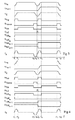
- the figure 3 represents an example of a timing diagram of signals characteristic of the control circuit 10 of the figure 2 for an example of a method for controlling column electrodes Ec n , Ec n + 1 , during the successive selection of a first line of the panel and a second line of the panel, which does not make it possible to optimize the reduction of the losses of energy in the case where a majority of the pixels of the panel are to be addressed.
- the switches Tdh n and Tdl n + 1 are closed and the switches Td1 n and Tdh n + 1 are open since it is desired to address only the pixel associated with the column electrode Ec n .
- the addressing step begins with the closing of the Tup switch, the switches Trh, Trl and Tdown being open.
- a positive current IL flows in inductance L causing the voltage V E to rise from 0 volts to Vpp.
- An increase of the voltage Vc n from 0 volts to Vpp is thus obtained while the voltage Vc n + 1 is maintained at 0 volts.
- the current IL is canceled when the voltage V E has almost reached Vpp.
- the diode D2 then prevents the flow of a negative current IL.
- the diode D4 makes it possible to avoid a discontinuity of the current when D2 cuts the current in now the potential at node D at Vpp.
- the Tup switch is then open.
- the voltage V E is maintained at Vpp by closing the switch Trh.
- the switch Trh is open and the Tdown switch is closed.
- a negative IL current then flows in the inductor L causing the voltage V E to decrease from Vpp to 0 volts.
- the switch Tdh n being closed, the voltage Vc n also decreases from Vpp to 0 volts.
- the switch Tdl n + 1 being closed, the voltage Vc n + 1 is maintained at 0 volts.
- Diode D1 prevents the flow of a positive current IL.
- the diode D3 makes it possible to avoid a current discontinuity when D1 cuts the current while maintaining the potential at node D at 0 volts.
- the Tdown switch is closed and the switch Trl is open to maintain the voltage V E at 0 volts.
- the switch Tdh n is kept closed and the switch Tdl n is kept open since, when selecting the second line, the corresponding pixel associated with the column electrode Ec n is to address.
- the switch Tdh n + 1 is closed and the switch Tdl n + 1 is open since, when selecting the second line, the corresponding pixel associated with the column electrode Ec n + 1 is to address.
- the switches Tup and Trh are successively closed as has been described previously for the instants t 1 and t 2 . Since the switches Tdh n and Tdh n + 1 are closed, the voltages Vc n and Vc n + 1 rise from 0 volts to Vpp. Finally, at the end of the addressing of the pixels of the second line, from the instant t 7 to the instant t 8 , the Tdown switch is closed to lower the voltage V E of Vpp to 0 volts.
- the previously described control method of circuit 10 is advantageous for displaying an image in which the pixels of the same column associated with two successively selected lines are at different states (addressed state or unaddressed state). The energy lost during the addressing of the pixels is then less than that lost by the control circuits of the column electrodes represented in FIG. figure 1 .
- the previously described control method of the circuit 10 is not advantageous as soon as there is a large number of pixels of the same columns which are addressed for several lines selected successively, which is the case for example for uniform images. . In this case, even higher energy losses are obtained than the losses obtained with the control circuits of the column electrodes represented in FIG. figure 1 since the column electrodes associated with pixels addressed for two successively selected lines go from Vpp to 0 and from 0 to Vpp for nothing.
- the present invention consists, when the pixels associated with the same column electrode are to be addressed during the successive selection of first and second lines, to maintain the high impedance column electrode during the transition phase, between the end of the selection of the first line and the beginning of the selection of the second line, during which the voltage V E successively passes from Vpp to 0 volts and then from 0 volts to Vpp. This makes it possible to maintain the column electrode substantially at Vpp and thus to reduce the energy losses with respect to the control method of the circuit 10 described above in connection with the figure 3 .
- the figure 4 represents an example of a timing diagram of signals characteristic of the control circuit 10 of the figure 2 for another example of a method for controlling the column electrodes Ec n , Ec n + 1 which makes it possible to obtain such a reduction in energy losses.
- the conventions used for the figure 3 are preserved.
- it is desired to address only the pixel associated with the column electrode Ec n when the selection of the first line and it is desired to address the pixels associated with the column electrodes Ec n and Ec n + 1 when selecting the second line.
- t ' i , i varying from 1 to 8, successive instants.
- the switches Tdl n , Tdh n + 1 , Tdl n + 1 , Tup, Tdown, Trh and Trl are controlled identically to what has been described previously between times t 1 and t 8 in relation to the figure 3 .
- the switch Tdh n is controlled, at times t ' 1 and t' 2 , in a manner identical to that described previously at times t 1 and t 2 in relation to the figure 3 .
- the switch Tdh n is open.
- the column electrode Ec n is then maintained at high impedance.
- the voltage Vc n thus varies little and remains substantially equal to Vpp.
- the switch Tdh n is kept open until time t ' 6 , that is to say during the whole of the transition phase during which the voltage V E goes from Vpp to 0 volts then from 0 volts to Vpp.
- the switch Tdh n is controlled at times t ' 7 and t' 8 , in a manner identical to that described above at times t 7 and t 8 in relation to the figure 3 .
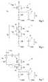
- the figure 5 represents a more detailed embodiment of the dedicated circuit 14 of a column electrode Ec.
- the switch Tdh consists of a single N-channel MOS transistor T whose drain is connected to the node E, whose source is connected to the column electrode Ec and whose substrate (in English "bulk” or "body”") is connected to the source of the transistor T.
- the gate of the transistor T is adapted to receive the control signal S Tdh .
- a diode D connected in parallel between the drain and the source of the transistor T, the cathode of the diode D being connected to the drain of the transistor T.
- the diode D corresponds to the "parasitic" diode between the drain and the substrate of the transistor T.
- Such an embodiment of the switch Tdh does not make it possible to implement the method of circuit control 10 previously described in connection with the figure 4 . Indeed, when the transistor T is open between times t ' 3 and t' 6 to maintain the column electrode Ec high impedance while the switch Tdl is itself open, the voltage V C is substantially equal at Vpp and that the voltage V E decreases from Vpp to 0 volts, a leakage current tends to flow from the ground GND to the node E via the column electrode Ec and the diode D. There is therefore a decrease in the voltage V C , which is not desirable.
- the figure 6 represents another more detailed embodiment of the dedicated circuit 14 of a column electrode Ec adapted to the implementation of the control method of the circuit 10 described above in connection with the figure 4 .
- the switch Tdh consists of two MOS transistors Ta and Tb N channel in series. A first power terminal of the transistor Ta is connected to the node E and the second power terminal of the transistor Ta is connected to a node F. A first power terminal of the transistor Tb is connected to the node F and the second power terminal of the transistor Tb is connected to the column electrode Ec.
- the substrates of transistors Ta and Tb are connected to node F.
- the gate of transistor Ta is adapted to receive a control signal S Ta and the gate of transistor Tb is adapted to receive a control signal S Tb .
- the control signals S Ta and S Tb can both be equal to the control signal S Tdh described above. In other words, the two switches Ta and Tb are open or closed simultaneously.
- diode Da connected in parallel across the terminals of the transistor Ta, the cathode of the diode Da being connected to the node E.
- the diode Da corresponds to the "parasitic" diode between the first power terminal and the substrate of the transistor Ta.
- a diode Db has been shown in parallel with terminals of the transistor Tb, the cathode of the diode Db being connected to the column electrode Ec.
- Diode Db corresponds to the "parasitic" diode between the second power terminal and the substrate of transistor Tb.
- the figure 7 represents an exemplary embodiment of the control of the transistors Ta and Tb of the figure 6 .
- the gates of the transistors Ta and Tb are connected to a node G.
- a resistor R is disposed between the nodes G and F.
- a switch Tdh 'and a current source SI are arranged in series between the node G and a node H.
- capacitor C ' is disposed between the nodes H and E.
- a diode D' connects the node H to a source of a reference potential Vcc, which is for example a few volts, the cathode of the diode D 'being connected to the node H.
- the control signal of the switch Tdh ' is equal to the signal S Tdh described above.
- the switch Tdh ' When the switch Tdh 'is closed, a current flows in the resistor R imposing a positive potential difference between the nodes G and F and therefore the application of a positive gate voltage to the gate of the transistors Ta and Tb which are then passersby.
- the capacitor C ' maintains the potential at the node H permanently at a level higher than the potential at the node E to ensure proper polarization of the gates of the transistors Ta, Tb. Indeed, when the node E is at 0 volts, the capacitor C 'is charged by the source of the reference potential Vcc and the potential at the node H rises slightly with respect to the potential at the node E. Thereafter, when the potential at the node E increases, the potential at the node H also increases by coupling effect due to the capacitor C '.
Landscapes
- Engineering & Computer Science (AREA)
- Physics & Mathematics (AREA)
- Power Engineering (AREA)
- Plasma & Fusion (AREA)
- Computer Hardware Design (AREA)
- General Physics & Mathematics (AREA)
- Theoretical Computer Science (AREA)
- Control Of Indicators Other Than Cathode Ray Tubes (AREA)
Applications Claiming Priority (1)
| Application Number | Priority Date | Filing Date | Title |
|---|---|---|---|
| FR0753713 | 2007-03-08 |
Publications (2)
| Publication Number | Publication Date |
|---|---|
| EP1968037A2 true EP1968037A2 (de) | 2008-09-10 |
| EP1968037A3 EP1968037A3 (de) | 2009-09-16 |
Family
ID=38572498
Family Applications (1)
| Application Number | Title | Priority Date | Filing Date |
|---|---|---|---|
| EP08102319A Withdrawn EP1968037A3 (de) | 2007-03-08 | 2008-03-05 | Vorrichtung und Verfahren zur Steuerung von Adresselektroden einer Plasma-Anzeigetafel |
Country Status (2)
| Country | Link |
|---|---|
| US (1) | US20090051626A1 (de) |
| EP (1) | EP1968037A3 (de) |
Family Cites Families (3)
| Publication number | Priority date | Publication date | Assignee | Title |
|---|---|---|---|---|
| JP4689078B2 (ja) * | 2001-05-31 | 2011-05-25 | パナソニック株式会社 | プラズマディスプレイ装置 |
| JP4652797B2 (ja) * | 2004-12-15 | 2011-03-16 | 日立プラズマディスプレイ株式会社 | プラズマディスプレイ装置及びその駆動方法 |
| JP5021932B2 (ja) * | 2005-12-15 | 2012-09-12 | パナソニック株式会社 | 表示パネルの駆動装置 |
-
2008
- 2008-03-05 EP EP08102319A patent/EP1968037A3/de not_active Withdrawn
- 2008-03-06 US US12/043,631 patent/US20090051626A1/en not_active Abandoned
Also Published As
| Publication number | Publication date |
|---|---|
| EP1968037A3 (de) | 2009-09-16 |
| US20090051626A1 (en) | 2009-02-26 |
Similar Documents
| Publication | Publication Date | Title |
|---|---|---|
| EP0237365B1 (de) | Lichtempfindliche Vorrichtung | |
| EP0815562B1 (de) | Verbessertes schieberegister mit mis-transistoren der gleichen priorität | |
| FR2868589A1 (fr) | Registre a decalage et son procede de commande | |
| EP0760149B1 (de) | Schieberegister mit gleich polarisierten mis-transistoren | |
| EP2311042B1 (de) | Schieberegister auf basis von feldeffekttransistoren | |
| FR2783342A1 (fr) | Appareil et procede d'elimination d'image residuelle pour un dispositif d'affichage a cristal liquide | |
| FR2787913A1 (fr) | Registre a decalage | |
| EP0145520B1 (de) | Bildschirm mit aktiver Matrix ohne Kreuzung von Zeilen- und Spaltenadressenleitungen | |
| FR2626705A1 (fr) | Montage d'affichage a matrice integree | |
| FR2704674A1 (fr) | Contrôleur d'un panneau d'affichage plasma et procédé de commande d'un tel panneau. | |
| FR2864678A1 (fr) | Dispositif d'affichage a electroluminescence et procede de commande de celui-ci | |
| EP2186081A1 (de) | Schieberegister für einen aktivmatrixflachbildschirm | |
| FR2705817A1 (fr) | Appareil d'alimentation électrique pour unité d'affichage à plasma et procédés associés. | |
| FR2626706A1 (fr) | Montage d'affichage a matrice integree | |
| EP0972282A1 (de) | Vorrichtung zur steuerung einer matrixanzeigestelle | |
| EP1156491B1 (de) | Verbesserungen an Schieberegistern unter alleiniger Verwendung von "MIS" Transistoren | |
| EP1608069B1 (de) | Verfahren zur Steuerung eines Analogschalters | |
| EP1700290B1 (de) | Bildanzeigeschirm und verfahren zur adressierung des schirms | |
| FR2739712A1 (fr) | Procede et appareil de modulation de niveaux de gris d'un affichage matriciel | |
| EP1697920B1 (de) | Vorrichtung zum anzeigen von bildern auf einer oled aktivmatrix | |
| FR2532777A1 (fr) | Circuit de translation de signaux | |
| EP1234300B1 (de) | Verfahren zur kompensation von durch demultiplexen eines analogen signals verursachten störungen in einer matrixanzeige | |
| EP1862999A2 (de) | Ansteuerung einer Plasmaanzeigetafel | |
| WO2023117605A1 (fr) | Ecran d'affichage comprenant des pixels d'affichage a diodes electroluminescentes | |
| FR2890459A1 (fr) | Procede de transition d'un affichage a cristaux liquides |
Legal Events
| Date | Code | Title | Description |
|---|---|---|---|
| PUAI | Public reference made under article 153(3) epc to a published international application that has entered the european phase |
Free format text: ORIGINAL CODE: 0009012 |
|
| AK | Designated contracting states |
Kind code of ref document: A2 Designated state(s): AT BE BG CH CY CZ DE DK EE ES FI FR GB GR HR HU IE IS IT LI LT LU LV MC MT NL NO PL PT RO SE SI SK TR |
|
| AX | Request for extension of the european patent |
Extension state: AL BA MK RS |
|
| PUAL | Search report despatched |
Free format text: ORIGINAL CODE: 0009013 |
|
| AK | Designated contracting states |
Kind code of ref document: A3 Designated state(s): AT BE BG CH CY CZ DE DK EE ES FI FR GB GR HR HU IE IS IT LI LT LU LV MC MT NL NO PL PT RO SE SI SK TR |
|
| AX | Request for extension of the european patent |
Extension state: AL BA MK RS |
|
| 17P | Request for examination filed |
Effective date: 20100309 |
|
| 17Q | First examination report despatched |
Effective date: 20100330 |
|
| AKX | Designation fees paid |
Designated state(s): DE FR GB IT |
|
| STAA | Information on the status of an ep patent application or granted ep patent |
Free format text: STATUS: THE APPLICATION IS DEEMED TO BE WITHDRAWN |
|
| 18D | Application deemed to be withdrawn |
Effective date: 20130223 |