EP1965415A2 - Method for manufacturing a semiconductor device and semiconductor device manufactured therefrom - Google Patents
Method for manufacturing a semiconductor device and semiconductor device manufactured therefrom Download PDFInfo
- Publication number
- EP1965415A2 EP1965415A2 EP08151862A EP08151862A EP1965415A2 EP 1965415 A2 EP1965415 A2 EP 1965415A2 EP 08151862 A EP08151862 A EP 08151862A EP 08151862 A EP08151862 A EP 08151862A EP 1965415 A2 EP1965415 A2 EP 1965415A2
- Authority
- EP
- European Patent Office
- Prior art keywords
- hetero
- semiconductor
- layer
- semiconductor layer
- etching stopper
- Prior art date
- Legal status (The legal status is an assumption and is not a legal conclusion. Google has not performed a legal analysis and makes no representation as to the accuracy of the status listed.)
- Granted
Links
Images


Classifications
-
- H—ELECTRICITY
- H10—SEMICONDUCTOR DEVICES; ELECTRIC SOLID-STATE DEVICES NOT OTHERWISE PROVIDED FOR
- H10D—INORGANIC ELECTRIC SEMICONDUCTOR DEVICES
- H10D62/00—Semiconductor bodies, or regions thereof, of devices having potential barriers
- H10D62/10—Shapes, relative sizes or dispositions of the regions of the semiconductor bodies; Shapes of the semiconductor bodies
- H10D62/13—Semiconductor regions connected to electrodes carrying current to be rectified, amplified or switched, e.g. source or drain regions
- H10D62/149—Source or drain regions of field-effect devices
- H10D62/151—Source or drain regions of field-effect devices of IGFETs
-
- H—ELECTRICITY
- H10—SEMICONDUCTOR DEVICES; ELECTRIC SOLID-STATE DEVICES NOT OTHERWISE PROVIDED FOR
- H10D—INORGANIC ELECTRIC SEMICONDUCTOR DEVICES
- H10D12/00—Bipolar devices controlled by the field effect, e.g. insulated-gate bipolar transistors [IGBT]
- H10D12/01—Manufacture or treatment
- H10D12/031—Manufacture or treatment of IGBTs
-
- H—ELECTRICITY
- H10—SEMICONDUCTOR DEVICES; ELECTRIC SOLID-STATE DEVICES NOT OTHERWISE PROVIDED FOR
- H10D—INORGANIC ELECTRIC SEMICONDUCTOR DEVICES
- H10D30/00—Field-effect transistors [FET]
- H10D30/60—Insulated-gate field-effect transistors [IGFET]
- H10D30/63—Vertical IGFETs
- H10D30/635—Vertical IGFETs having no inversion channels, e.g. vertical accumulation channel FETs [ACCUFET] or normally-on vertical IGFETs
-
- H—ELECTRICITY
- H10—SEMICONDUCTOR DEVICES; ELECTRIC SOLID-STATE DEVICES NOT OTHERWISE PROVIDED FOR
- H10D—INORGANIC ELECTRIC SEMICONDUCTOR DEVICES
- H10D62/00—Semiconductor bodies, or regions thereof, of devices having potential barriers
- H10D62/80—Semiconductor bodies, or regions thereof, of devices having potential barriers characterised by the materials
- H10D62/82—Heterojunctions
-
- H—ELECTRICITY
- H10—SEMICONDUCTOR DEVICES; ELECTRIC SOLID-STATE DEVICES NOT OTHERWISE PROVIDED FOR
- H10D—INORGANIC ELECTRIC SEMICONDUCTOR DEVICES
- H10D62/00—Semiconductor bodies, or regions thereof, of devices having potential barriers
- H10D62/80—Semiconductor bodies, or regions thereof, of devices having potential barriers characterised by the materials
- H10D62/83—Semiconductor bodies, or regions thereof, of devices having potential barriers characterised by the materials being Group IV materials, e.g. B-doped Si or undoped Ge
- H10D62/832—Semiconductor bodies, or regions thereof, of devices having potential barriers characterised by the materials being Group IV materials, e.g. B-doped Si or undoped Ge being Group IV materials comprising two or more elements, e.g. SiGe
- H10D62/8325—Silicon carbide
Definitions
- the invention relates generally to a methods for manufacturing a semiconductor device and particularly, but not exclusively, to a method of manufacturing a semiconductor device including a hetero-semiconductor region hetero-joined to a semiconductor substrate and to a semiconductor device manufactured according to the method. Aspects of the invention relate to a method and to a device.
- Silicon carbide has dielectric breakdown field strength ten times as large as that of silicon and, like silicon, silicon carbide can be subjected to thermal oxidation. Therefore, silicon carbide attracts attention as the next generation of semiconductor materials.
- application to power conversion elements is desirable, and power transistors with high voltage resistance and low loss that use silicon carbide as a material have recently been proposed. It is necessary to decrease on-resistance in order to decrease the loss of a power transistor, and a power transistor that can effectively decrease on-resistance is desired.
- a semiconductor device in which a hetero-semiconductor region composed of polycrystalline silicon and having a band gap different from that of silicon carbide is formed in contact with a predetermined region of a first main surface of a high-concentration N-type silicon carbide semiconductor substrate on which an N-type silicon carbide epitaxial layer having a lower impurity concentration than that of the silicon carbide substrate is formed from, for example, Japanese Unexamined Patent Application Publication No. 2003-318398 .
- the silicon carbide epitaxial layer is hetero-joined to the hetero-semiconductor region.
- a gate electrode is formed, through a gate insulating film, adjacent to the hetero-junction between the silicon carbide epitaxial layer and the hetero-semiconductor region.
- a source electrode is formed in contact with the hetero-semiconductor region.
- a drain electrode is formed in contact with the silicon carbide substrate, i.e., in contact with the silicon carbide semiconductor substrate. Further, the source electrode and the gate electrode are electrically insulated from each other through an interlayer insulating film. As a result, the semiconductor device functions as a field effect transistor.
- the barrier height of the hetero-junction between the hetero-semiconductor region and the silicon carbide epitaxial layer is changed using an electric field from the gate electrode to perform a switching operation. Therefore, the on-resistance can be decreased because of no voltage drop in the channel region. Also, when a high voltage is applied between the source electrode and the drain electrode, an electric field is terminated in an accumulation layer formed on the hetero-semiconductor region side of the hetero-junction interface, and thus breakdown does not occur in the hetero-semiconductor region, thereby securing high voltage resistance between the source electrode and the drain electrode.
- Japanese Unexamined Patent Application Publication No. 2003-318398 discloses forming a hetero semiconductor layer as a hetero semiconductor region on a silicon carbide semiconductor substrate.
- the hetero semiconductor layer is patterned by partially removing it until the silicon carbide semiconductor substrate is exposed to form a groove.
- a gate insulating film and a gate electrode are formed in the groove.
- the hetero semiconductor layer When the hetero semiconductor layer is partially removed to form the groove, wet etching is used, which causes etching damage to the hetero-junction between the hetero semiconductor layer and the silicon carbide semiconductor substrate. Further, the width of the opening of the groove is increased according to the thickness of the hetero semiconductor layer because wet etching is isotropic etching, thereby increasing the size of the semiconductor device.
- Embodiments of the invention may provide a method of manufacturing a semiconductor device which allow miniaturization of the semiconductor device.
- Other aims and advantages of the invention will become apparent from the following description, claims and drawings.
- a method for manufacturing a semiconductor device including a semiconductor substrate, a hetero-semiconductor region that forms a hetero-junction to a first surface of the semiconductor substrate and is composed of a hetero-semiconductor material having a different band gap from that of a semiconductor material of the semiconductor substrate, a gate insulating film formed in contact with a hetero-junction between the semiconductor substrate and the hetero-semiconductor region, a gate electrode formed in contact with the gate insulating film, a source electrode formed in contact with the hetero-semiconductor region, and a drain electrode formed in contact with the semiconductor substrate, the method comprising forming a first hetero-semiconductor layer on the first surface of the semiconductor substrate, the first hetero-semiconductor layer including the hetero-semiconductor material, forming an etching stopper layer at a predetermined position on a first surface of the first hetero-semiconductor layer opposite to
- removing the etching stopper layer comprises etching at least a portion of the second hetero-semiconductor layer on a first surface of the etching stopper layer until the etching stopper layer is exposed.
- removing the etching stopper layer comprises forming a photoresist on a first surface of the second hetero-semiconductor layer, the photoresist having a hole positioned above the etching stopper layer; and wherein etching at least a portion of the second hetero-semiconductor layer further comprises etching the second hetero-semiconductor layer through the hole until the etching stopper layer is exposed.
- removing the etching stopper layer comprises selectively removing the etching stopper layer by wet etching after etching at least the portion of the second hetero-semiconductor layer.
- the method may comprise polishing the second hetero-semiconductor layer until the etching stopper layer is exposed before removing the etching stopper layer.
- removing the etching stopper layer further comprises selectively removing the etching stopper layer by wet etching after polishing the second hetero-semiconductor layer.
- the method may comprise, after thermally oxidizing the first hetero-semiconductor layer removing a portion formed by thermal oxidation of the first hetero-semiconductor layer, forming a gate insulating film in contact with the semiconductor substrate, the first hetero-semiconductor layer, and the second hetero-semiconductor layer and forming the gate electrode in contact with a hetero-junction between the semiconductor substrate and the first hetero-semiconductor layer through the gate insulating film.
- the method may comprise removing a thermally oxidized portion of the first hetero-semiconductor layer by wet etching.
- the material of the etching stopping layer is silicon oxide or silicon nitride.
- a thickness of the first hetero-semiconductor layer is such that the first hetero-semiconductor layer is completely converted to a silicon oxide layer in response to thermally oxidizing the first hetero-semiconductor layer.
- the hetero-semiconductor material is one of single crystal silicon, polycrystalline silicon and amorphous silicon.
- the semiconductor material of the semiconductor substrate is one of silicon carbide, gallium nitride and diamond.
- a method for manufacturing a semiconductor device may comprise forming a first hetero-semiconductor layer on a first surface of a semiconductor substrate, the first hetero-semiconductor layer including a hetero-semiconductor material, forming an etching stopper layer at a predetermined position on a first surface of the first hetero-semiconductor layer opposite the semiconductor substrate, the etching stopper layer including a material having a different etching rate from that of the first hetero-semiconductor material, forming a second hetero-semiconductor layer on the first hetero-semiconductor layer and the etching stopper layer, the second hetero-semiconductor layer including a hetero-semiconductor material, removing the etching stopper layer and thermally oxidizing the first hetero-semiconductor layer.
- a semiconductor device manufactured according to a first embodiment is described with reference to FIG. 1 .
- a N-type silicon carbide epitaxial layer 2 at a lower impurity concentration than that of a high-concentration N-type silicon carbide substrate 1 is formed on a first main surface of the silicon carbide substrate 1, i.e., the front surface side thereof, to form a silicon carbide semiconductor substrate 100.
- the semiconductor device according to the first embodiment further includes an N-type hetero-semiconductor region 10 that forms a hetero-junction to the first surface of the silicon carbide semiconductor substrate 100, i.e., the front surface thereof.
- the hetero-semiconductor region 10 is composed of polycrystalline silicon, which is a hetero-semiconductor material having a different band gap from that of silicon carbide used as a semiconductor material of the silicon carbide semiconductor substrate 100.
- the hetero-semiconductor region 10 includes an N-type first hetero-semiconductor layer 3 formed on the surface of the silicon carbide epitaxial layer 2 of the silicon carbide semiconductor substrate 100 and an N-type second hetero-semiconductor layer 5 formed on the first main surface of the first hetero-semiconductor layer 3, i.e., the front surface thereof.
- the first hetero-semiconductor layer 3 and the second hetero-semiconductor layer 5 are composed of polycrystalline silicon.
- the semiconductor device further includes a gate insulating film 6 formed in contact with a hetero-junction between the silicon carbide epitaxial layer 2 of the silicon carbide semiconductor substrate 100 and the first hetero-semiconductor layer 3 of the hetero-semiconductor region 10.
- a gate electrode 7 is formed in contact with the gate insulating film 6, a source electrode 8 is formed in contact with the second hetero-semiconductor layer 5 of the hetero-semiconductor region 10, and a drain electrode 9 is formed in contact with the back side of the silicon carbide substrate of the silicon carbide semiconductor substrate 100.
- the gate electrode 7 and the source electrode 8 are electrically insulated from each other through an interlayer insulating film 33.
- the semiconductor device functions as a field effect transistor having a vertical structure when the barrier height of the hetero-junction between the silicon carbide epitaxial layer 2 and the first hetero-semiconductor layer 3 is changed by an electric field applied from the gate electrode 7.
- hetero-junction drive end the portion in contact with the gate insulating film 6 is referred to as the "hetero-junction drive end".
- the silicon carbide semiconductor substrate 100 including the silicon carbide substrate 1 and the silicon carbide epitaxial layer 2 laminated on the first main surface side, i.e., the front surface side of the silicon carbide substrate 1, is prepared.
- polycrystalline silicon, which is a hetero-semiconductor material is deposited to, for example, 200 A, on the surface of the silicon carbide epitaxial layer 2 of the silicon carbide semiconductor substrate 100 to form the first hetero-semiconductor layer 3.
- an etching stopper layer 4 composed of silicon oxide, which is a material having a different etching rate from that of polycrystalline silicon used as a hetero-semiconductor material, is formed in a thickness of, for example, 0.1 ⁇ m.
- the etching stopping layer 4 is formed at a predetermined position of the first surface, i.e., the front surface, of the first hetero-semiconductor layer 3.
- polycrystalline silicon is deposited to, for example, 0.4 ⁇ m, in contact with the first main surface, i.e., the front surface, of the first hetero-semiconductor layer 3 and the etching stopper 4.
- arsenic ions 30 are implanted as an impurity dopant, for example, with an acceleration voltage of 70 KeV and in a dosage of 5 ⁇ 10 15 cm -3 to form the N-type first hetero-semiconductor layer 3 and the N-type second hetero-semiconductor layer 5.
- an etching gas used for dry etching is selected so that the etching selection ratio of the polycrystalline silicon that constitutes the second hetero-semiconductor layer 5 is higher than that of the silicon oxide that constitutes the etching stopper layer 4.
- the etching stopper layer 4 is little etched. Namely, the second hetero-semiconductor layer 5 can be stably partially etched on the surface of the etching stopper layer 4.
- the thickness of the etching stopper layer 4 is, for example, 0.1 ⁇ m, plasma damage due to dry etching does not occur in the portion of the first hetero-semiconductor layer 3 that is covered with the etching stopper layer 4.
- SOG Spin On Glass
- the surface of the second hetero-semiconductor layer 5 may be planarized and then entirely etched back so as to expose the etching stopper layer 4.
- the etching stopper layer 4 composed of silicon oxide is next selectively removed by wet etching with an aqueous solution of buffered hydrofluoric acid as shown in FIG. 2E .
- the aqueous solution of buffered hydrofluoric acid is selected as an aqueous solution used in wet etching so that the etching selection ratio of the silicon oxide that constitutes the etching stopper layer 4 is higher than that of the polycrystalline silicon that constitutes the first and second hetero-semiconductor layers 3 and 5. Therefore, even if an amount of overetching is large, the first and second hetero-semiconductor layers 3 and 5 are little etched. In this manner, the etching stopper layer 4 can be selectively stably etched.
- the first and second hetero-semiconductor layers 3 and 5 are thermally oxidized.
- the thermal oxidation is performed under a condition in which the portion of the first hetero-semiconductor layer 3 covered with the etching stopper layer 4 is completely oxidized in the thickness direction.
- the portion of the first hetero-semiconductor layer 3 covered with the etching stopper layer 4 is completely converted to a silicon oxide layer 32, which is an oxide layer in the thickness direction.
- the conditions for thermal oxidation are determined according to the thickness of the first hetero-semiconductor layer 3
- the thickness of the first hetero-semiconductor layer 3 may be determined according to the thermal oxidation conditions as long as the portion of the first hetero-semiconductor layer 3 covered with the etching stopper layer 4 can be completely oxidized by thermal oxidation in the thickness direction.
- the silicon oxide layer 32 is removed by wet etching with an aqueous solution of buffered hydrofluoric acid to expose the silicon carbide epitaxial layer 2.
- this embodiment of the method includes forming the etching stopper layer 4 on the surface of the first hetero-semiconductor layer 3, forming the second hetero-semiconductor layer 5 in contact with the first hetero-semiconductor layer 3 and the etching stopper layer 4, removing the etching stopper layer 4, thermally oxidizing the portion of the first hetero-semiconductor layer 3 that is covered with the etching stopper layer 4 to convert the portion to the silicon oxide layer 32, and then removing the silicon oxide layer 32 by wet etching.
- a hetero-junction drive end is formed while suppressing the occurrence of plasma damage due to dry etching in the first hetero-semiconductor layer 3 and the silicon carbide epitaxial layer 2 near the hetero-junction drive end.
- the gate insulating film 6 is deposited to a thickness of, for example, 1000 ⁇ , on the silicon carbide epitaxial layer 2 and the second hetero-semiconductor layer 5 so as to contact the hetero-junction between the silicon carbide semiconductor substrate 100 and the hetero-semiconductor region 10.
- polycrystalline silicon is deposited to a thickness of, for example, 5000 ⁇ , to form a polycrystalline silicon layer 40 in contact with the gate insulating film 6.
- an impurity is introduced into the polycrystalline silicon layer 40, and then the polycrystalline silicon layer 40 is patterned by photolithography and etching to form the gate electrode 7 as shown in FIG. 2J .
- the gate electrode 7 is adjacent to, through the gate insulating film 6, the hetero-junction between the silicon carbide semiconductor substrate 100 and the hetero-semiconductor region 10.
- the interlayer insulating film 33 is deposited to, for example, 2 ⁇ m, on the surfaces of the gate insulating film 6 and the gate electrode 7. Then, a contact hole is formed in the interlayer insulating film 33, and aluminum is deposited to, for example, 2 ⁇ m, in contact with the hetero-semiconductor region 10 to form the source electrode 8.
- the source electrode 8 contacts the hetero-semiconductor region 10 in a rear portion in the direction perpendicular to the drawing.
- titanium and aluminum are deposited to, for example, 0.1 ⁇ m and 2 ⁇ m, respectively, in contact with the back side of the silicon carbide substrate 1 to form the drain electrode 9.
- the semiconductor device shown in FIG. 1 is completed by performing the above-described steps.
- the hetero-junction drive end can be formed while suppressing the occurrence of plasma damage due to dry etching in the first hetero-semiconductor layer 3 and the silicon carbide epitaxial layer 2 near the hetero-junction drive end that contacts the gate insulating film 6.
- the thickness of the etching stopper layer 4 is 0.1 ⁇ m, and thus even when the second hetero-semiconductor layer 5 is etched by photolithography and dry etching, plasma damage due to dry etching does not occur in the portion of the first hetero-semiconductor layer 3 that is covered with the etching stopper layer 4. Therefore, plasma damage due to dry etching can be suppressed from occurring in the first hetero-semiconductor layer 3 and the silicon carbide epitaxial layer 2 near the hetero-junction drive end.
- the hetero-junction drive end which contacts the gate insulating film 6, is formed at the hetero-junction interface to which an electric field of the gate electrode 7 is applied, plasma damage can be suppressed, and a drive current can be increased. Namely, the on-resistance can be decreased as compared with a semiconductor device manufactured by conventional methods.
- the first hetero-semiconductor layer 3 is formed on the surface of the silicon carbide epitaxial layer 2
- the etching stopper layer 4 is formed on the surface of the first hetero-semiconductor layer 3 using silicon oxide, which is a material having an etching rate different from that of the polycrystalline silicon forming the first hetero-semiconductor layer 3
- the second hetero-semiconductor layer 5 is formed in contact with the first hetero-semiconductor layer 3 and the etching stopper layer 4, and the etching stopper layer is removed to expose the first hetero-semiconductor layer 3 and thin a portion of the hetero-semiconductor region 10.
- etching of a portion to be thinned can be easily controlled (control of the residual thickness) by changing the thickness of the first hetero-semiconductor layer 3, and the occurrence of plasma damage due to dry etching can be securely suppressed.
- the etching stopper layer 4 can be wet-etched without etching of the first hetero-semiconductor layer 3 and the second hetero-semiconductor layer 5.
- the portion of the first hetero-semiconductor layer 3 that is covered with the etching stopper layer 4 can be securely exposed to securely thin a portion of the hetero-semiconductor region 10.
- the hetero-semiconductor region 10 having a predetermined thickness or more can be formed by forming the second hetero-semiconductor layer 5 of 0.4 ⁇ m on the surface of the first hetero-semiconductor layer 3 of 200 A, and thus source resistance can be decreased.
- the hetero-semiconductor region 10 having a predetermined thickness or more can be formed, and thus arsenic ions 30 to be implanted can be prevented from passing through the hetero-semiconductor region 10 and being implanted into the silicon carbide epitaxial layer 2 in the step of forming the hetero-semiconductor region 10 by implanting the arsenic ions 30 as impurities.
- the etching gas is selected so that the etching selection ratio of polycrystalline silicon that constitutes the second hetero-semiconductor layer 5 is higher than that of silicon oxide that constitutes the etching stopper layer 4. Therefore, even when an amount of overetching is large, the etching stopper layer 4 is little etched, and thus the second hetero-semiconductor layer 5 on the surface of the etching stopper layer 4 can be stably etched.
- the etching stopper layer 4 is composed of silicon oxide, the etching stopper layer 4 can be selectively, easily and stably removed, without etching the first and second hetero-semiconductor layers 3, 5, by wet etching with an aqueous solution of buffered hydrofluoric acid that shows a higher etching selection ratio for the silicon oxide of the etching stopper layer 4 than that for the polycrystalline silicon of the first and second hetero-semiconductor layers 3, 5.
- silicon carbide is used as a semiconductor material that constitutes the silicon carbide semiconductor substrate 100, and thus a semiconductor device with high voltage resistance can be realized.
- polycrystalline silicon is used as the hetero-semiconductor material that constitutes the hetero-semiconductor region 10, and thus a process for controlling conductivity of the hetero-semiconductor region 10 can be simply performed.
- FIGS. 3A and 3B a method for manufacturing a semiconductor device according to a second embodiment is described with reference to FIGS. 3A and 3B mainly with respect to differences from the method according to the first embodiment.
- the same structure as in the semiconductor device manufactured according to the first embodiment is denoted by the same reference numeral, and description is omitted.
- the semiconductor device according to the second embodiment is different from the first embodiment only in the shape of the second hetero-semiconductor layer 5.
- the second hetero-semiconductor layer 5 on the surface of the etching stopper layer 4 is polished in the step of etching the second hetero-semiconductor layer 5 on the surface of the etching stopper layer 4.
- the second hetero-semiconductor layer 5 on the surface of the etching stopper layer 4 is polished by CMP (Chemical Mechanical Polishing) after the step shown in FIG. 2C .
- CMP Chemical Mechanical Polishing
- the steps shown in FIG. 2F to 2K are performed in the same manner as in the first embodiment to complete the semiconductor device of the second embodiment.
- the second hetero-semiconductor layer 5 can be planarized, and the same effects as in the first embodiment can be achieved.
- the drain electrode 9 and the source electrode 8 are disposed opposite to each other with the silicon carbide epitaxial layer 2 provided therebetween so that the characteristic portion is applied to a so-called vertical structure field effect transistor in which a current flows in the vertical direction.
- the drain electrode 9 and the source electrode 8 can be disposed on the same main surface so that the invention can be applied to a so-called horizontal structure field effect transistor in which a current flows in a transverse direction.
- the silicon carbide semiconductor substrate 100, the hetero-semiconductor region 10 and the first and second hetero-semiconductor layers 3 and 5 are N-type.
- these members are not particularly limited to this type, so P-type may be used.
- silicon carbide is used as the semiconductor material that constitutes the silicon carbide semiconductor substrate 100.
- the semiconductor material is not limited to this, and gallium nitride or diamond may be used.
- polycrystalline silicon is used as the hetero-semiconductor material that constitutes the hetero-semiconductor region 10.
- the hetero-semiconductor material is not limited to this, however, and single crystal silicon, amorphous silicon, silicon germanium or gallium arsenide may be used alternatively or in addition thereto.
- Silicon oxide is used as a material for the etching stopper layer 4 in each of the described embodiments.
- silicon nitride may be used, for example, as long as it has a different etching rate from that of polycrystalline silicon used as the hetero-semiconductor material.
- the N-type first hetero-semiconductor layer 3 and the N-type second hetero-semiconductor layer 5 are formed by ion implantation of impurities, specifically arsenic ions 30.
- impurities specifically arsenic ions 30.
- various methods of introducing impurities are contemplated.
- impurities may be introduced by a diffusion method.
- the second hetero-semiconductor layer 5 on the surface of the etching stopper layer 4 is partially etched by photolithography and dry etching.
- the etching is not limited to this method.
- SOG may be applied on the surface of the second hetero-semiconductor layer 5 to planarize the surface of the second hetero-semiconductor layer 5, and then the planarized entire surface may be etched back to expose the etching stopper layer 4, thereby realizing the structure shown in FIGS. 3A and 3B .
- the conditions for thermal oxidation are determined according to the thickness of the first hetero-semiconductor layer 3.
- the thermal oxidation is not limited to this, and the thickness of the first hetero-semiconductor layer 3 may be determined according to the conditions of thermal oxidation as long as the portion of the first hetero-semiconductor layer 3 covered with the etching stopper layer 4 can be completely oxidized in this step in the thickness direction.
Landscapes
- Electrodes Of Semiconductors (AREA)
- Junction Field-Effect Transistors (AREA)
- Recrystallisation Techniques (AREA)
Abstract
Description
- The invention relates generally to a methods for manufacturing a semiconductor device and particularly, but not exclusively, to a method of manufacturing a semiconductor device including a hetero-semiconductor region hetero-joined to a semiconductor substrate and to a semiconductor device manufactured according to the method. Aspects of the invention relate to a method and to a device.
- Silicon carbide has dielectric breakdown field strength ten times as large as that of silicon and, like silicon, silicon carbide can be subjected to thermal oxidation. Therefore, silicon carbide attracts attention as the next generation of semiconductor materials. In particular, application to power conversion elements is desirable, and power transistors with high voltage resistance and low loss that use silicon carbide as a material have recently been proposed. It is necessary to decrease on-resistance in order to decrease the loss of a power transistor, and a power transistor that can effectively decrease on-resistance is desired. Therefore, there is known a semiconductor device in which a hetero-semiconductor region composed of polycrystalline silicon and having a band gap different from that of silicon carbide is formed in contact with a predetermined region of a first main surface of a high-concentration N-type silicon carbide semiconductor substrate on which an N-type silicon carbide epitaxial layer having a lower impurity concentration than that of the silicon carbide substrate is formed from, for example, Japanese Unexamined Patent Application Publication No.
2003-318398 - In this semiconductor device, the silicon carbide epitaxial layer is hetero-joined to the hetero-semiconductor region. In addition, a gate electrode is formed, through a gate insulating film, adjacent to the hetero-junction between the silicon carbide epitaxial layer and the hetero-semiconductor region. A source electrode is formed in contact with the hetero-semiconductor region. Also, a drain electrode is formed in contact with the silicon carbide substrate, i.e., in contact with the silicon carbide semiconductor substrate. Further, the source electrode and the gate electrode are electrically insulated from each other through an interlayer insulating film. As a result, the semiconductor device functions as a field effect transistor. The barrier height of the hetero-junction between the hetero-semiconductor region and the silicon carbide epitaxial layer is changed using an electric field from the gate electrode to perform a switching operation. Therefore, the on-resistance can be decreased because of no voltage drop in the channel region. Also, when a high voltage is applied between the source electrode and the drain electrode, an electric field is terminated in an accumulation layer formed on the hetero-semiconductor region side of the hetero-junction interface, and thus breakdown does not occur in the hetero-semiconductor region, thereby securing high voltage resistance between the source electrode and the drain electrode.
- In a conventional method for manufacturing the semiconductor device previously described, Japanese Unexamined Patent Application Publication No.
2003-318398 - When the hetero semiconductor layer is partially removed to form the groove, wet etching is used, which causes etching damage to the hetero-junction between the hetero semiconductor layer and the silicon carbide semiconductor substrate. Further, the width of the opening of the groove is increased according to the thickness of the hetero semiconductor layer because wet etching is isotropic etching, thereby increasing the size of the semiconductor device.
- It is an aim of the invention to address this issue and to improve upon known technology. Embodiments of the invention may provide a method of manufacturing a semiconductor device which allow miniaturization of the semiconductor device. Other aims and advantages of the invention will become apparent from the following description, claims and drawings.
- Aspects of the invention therefore provide a method and a device as claimed in the appended claims.
- According to another aspect of the invention for which protection is sought there is provided a method for manufacturing a semiconductor device including a semiconductor substrate, a hetero-semiconductor region that forms a hetero-junction to a first surface of the semiconductor substrate and is composed of a hetero-semiconductor material having a different band gap from that of a semiconductor material of the semiconductor substrate, a gate insulating film formed in contact with a hetero-junction between the semiconductor substrate and the hetero-semiconductor region, a gate electrode formed in contact with the gate insulating film, a source electrode formed in contact with the hetero-semiconductor region, and a drain electrode formed in contact with the semiconductor substrate, the method comprising forming a first hetero-semiconductor layer on the first surface of the semiconductor substrate, the first hetero-semiconductor layer including the hetero-semiconductor material, forming an etching stopper layer at a predetermined position on a first surface of the first hetero-semiconductor layer opposite to the semiconductor substrate, the etching stopper layer including a material having a different etching rate from that of the first hetero-semiconductor material, forming a second hetero-semiconductor layer on the first hetero-semiconductor layer and the etching stopper layer, the second hetero-semiconductor layer including a hetero-semiconductor material, removing the etching stopper layer and thermally oxidizing the first hetero-semiconductor layer.
- In an embodiment, removing the etching stopper layer comprises etching at least a portion of the second hetero-semiconductor layer on a first surface of the etching stopper layer until the etching stopper layer is exposed.
- In an embodiment, removing the etching stopper layer comprises forming a photoresist on a first surface of the second hetero-semiconductor layer, the photoresist having a hole positioned above the etching stopper layer; and wherein etching at least a portion of the second hetero-semiconductor layer further comprises etching the second hetero-semiconductor layer through the hole until the etching stopper layer is exposed.
- In an embodiment, removing the etching stopper layer comprises selectively removing the etching stopper layer by wet etching after etching at least the portion of the second hetero-semiconductor layer.
- The method may comprise polishing the second hetero-semiconductor layer until the etching stopper layer is exposed before removing the etching stopper layer.
- In an embodiment, removing the etching stopper layer further comprises selectively removing the etching stopper layer by wet etching after polishing the second hetero-semiconductor layer.
- The method may comprise, after thermally oxidizing the first hetero-semiconductor layer removing a portion formed by thermal oxidation of the first hetero-semiconductor layer, forming a gate insulating film in contact with the semiconductor substrate, the first hetero-semiconductor layer, and the second hetero-semiconductor layer and forming the gate electrode in contact with a hetero-junction between the semiconductor substrate and the first hetero-semiconductor layer through the gate insulating film.
- The method may comprise removing a thermally oxidized portion of the first hetero-semiconductor layer by wet etching.
- In an embodiment, the material of the etching stopping layer is silicon oxide or silicon nitride.
- In an embodiment, a thickness of the first hetero-semiconductor layer is such that the first hetero-semiconductor layer is completely converted to a silicon oxide layer in response to thermally oxidizing the first hetero-semiconductor layer.
- In an embodiment, the hetero-semiconductor material is one of single crystal silicon, polycrystalline silicon and amorphous silicon.
- In an embodiment, the semiconductor material of the semiconductor substrate is one of silicon carbide, gallium nitride and diamond.
- According to another aspect of the invention for which protection is sought there is provided a semiconductor device made according to one or more of the methods set out above.
- For example, a method for manufacturing a semiconductor device may comprise forming a first hetero-semiconductor layer on a first surface of a semiconductor substrate, the first hetero-semiconductor layer including a hetero-semiconductor material, forming an etching stopper layer at a predetermined position on a first surface of the first hetero-semiconductor layer opposite the semiconductor substrate, the etching stopper layer including a material having a different etching rate from that of the first hetero-semiconductor material, forming a second hetero-semiconductor layer on the first hetero-semiconductor layer and the etching stopper layer, the second hetero-semiconductor layer including a hetero-semiconductor material, removing the etching stopper layer and thermally oxidizing the first hetero-semiconductor layer.
- Within the scope of this application it is envisaged that the various aspects, embodiments, examples, features and alternatives set out in the preceding paragraphs, in the claims and/or in the following description and drawings may be taken individually or in any combination thereof.
- The present invention will now be described, by way of example only, with reference to the accompanying drawings in which:
-
FIG. 1 is a cross-sectional view of a semiconductor device manufactured using a method according to a first embodiment of the invention; -
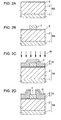
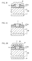
FIGS. 2A to 2K are cross-sectional views of the semiconductor device ofFIG. 1 after respective steps of the method according to the first embodiment; and -
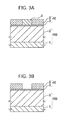
FIGS. 3A and 3B are cross-sectional views of a semiconductor device after respective steps of a method for manufacturing according to a second embodiment of the invention. - First, a semiconductor device manufactured according to a first embodiment is described with reference to
FIG. 1 . In this semiconductor device, a N-type silicon carbideepitaxial layer 2 at a lower impurity concentration than that of a high-concentration N-typesilicon carbide substrate 1 is formed on a first main surface of thesilicon carbide substrate 1, i.e., the front surface side thereof, to form a siliconcarbide semiconductor substrate 100. The semiconductor device according to the first embodiment further includes an N-type hetero-semiconductor region 10 that forms a hetero-junction to the first surface of the siliconcarbide semiconductor substrate 100, i.e., the front surface thereof. The hetero-semiconductor region 10 is composed of polycrystalline silicon, which is a hetero-semiconductor material having a different band gap from that of silicon carbide used as a semiconductor material of the siliconcarbide semiconductor substrate 100. - The hetero-
semiconductor region 10 includes an N-type first hetero-semiconductor layer 3 formed on the surface of the silicon carbideepitaxial layer 2 of the siliconcarbide semiconductor substrate 100 and an N-type second hetero-semiconductor layer 5 formed on the first main surface of the first hetero-semiconductor layer 3, i.e., the front surface thereof. Namely, the first hetero-semiconductor layer 3 and the second hetero-semiconductor layer 5 are composed of polycrystalline silicon. - The semiconductor device further includes a
gate insulating film 6 formed in contact with a hetero-junction between the silicon carbideepitaxial layer 2 of the siliconcarbide semiconductor substrate 100 and the first hetero-semiconductor layer 3 of the hetero-semiconductor region 10. Agate electrode 7 is formed in contact with thegate insulating film 6, a source electrode 8 is formed in contact with the second hetero-semiconductor layer 5 of the hetero-semiconductor region 10, and adrain electrode 9 is formed in contact with the back side of the silicon carbide substrate of the siliconcarbide semiconductor substrate 100. Thegate electrode 7 and the source electrode 8 are electrically insulated from each other through aninterlayer insulating film 33. AlthoughFIG. 1 shows the construction in which the second hetero-semiconductor layer 5 and the source electrode 8 are insulated from each other through thegate insulating film 6, the second hetero-semiconductor layer 5 of the hetero-semiconductor region 10 contacts the source electrode 8 in a rear portion in the direction perpendicular to the drawing. The semiconductor device functions as a field effect transistor having a vertical structure when the barrier height of the hetero-junction between the silicon carbideepitaxial layer 2 and the first hetero-semiconductor layer 3 is changed by an electric field applied from thegate electrode 7. Hereinafter, in the hetero-junction between the silicon carbideepitaxial layer 2 and the first hetero-semiconductor layer 3, i.e., the hetero-junction interface, the portion in contact with thegate insulating film 6 is referred to as the "hetero-junction drive end". - Next, the method for manufacturing the semiconductor device according to
FIG. 1 is described with reference toFIGS. 2A to 2K . First, as shown inFIG. 2A , the siliconcarbide semiconductor substrate 100 including thesilicon carbide substrate 1 and the silicon carbideepitaxial layer 2 laminated on the first main surface side, i.e., the front surface side of thesilicon carbide substrate 1, is prepared. Then, polycrystalline silicon, which is a hetero-semiconductor material, is deposited to, for example, 200 A, on the surface of the silicon carbideepitaxial layer 2 of the siliconcarbide semiconductor substrate 100 to form the first hetero-semiconductor layer 3. - As shown in
FIG. 2B , next an etching stopper layer 4 composed of silicon oxide, which is a material having a different etching rate from that of polycrystalline silicon used as a hetero-semiconductor material, is formed in a thickness of, for example, 0.1 µm. The etching stopping layer 4 is formed at a predetermined position of the first surface, i.e., the front surface, of the first hetero-semiconductor layer 3. Next, as shown inFIG. 2C , polycrystalline silicon is deposited to, for example, 0.4 µm, in contact with the first main surface, i.e., the front surface, of the first hetero-semiconductor layer 3 and the etching stopper 4. Then,arsenic ions 30 are implanted as an impurity dopant, for example, with an acceleration voltage of 70 KeV and in a dosage of 5 × 1015 cm-3 to form the N-type first hetero-semiconductor layer 3 and the N-type second hetero-semiconductor layer 5. - Next, as shown in
FIG. 2D , in photolithography anddry etching photoresist 31 is applied on the second hetero-semiconductor layer 5, and the second hetero-semiconductor layer 5 is partially etched on the first main surface of the etching stopper layer 4, i.e., the surface opposite to the contact surface between the first and second hetero-semiconductor layers semiconductor layer 5 is higher than that of the silicon oxide that constitutes the etching stopper layer 4. Therefore, even if an amount of overetching is large, the etching stopper layer 4 is little etched. Namely, the second hetero-semiconductor layer 5 can be stably partially etched on the surface of the etching stopper layer 4. In addition, since the thickness of the etching stopper layer 4 is, for example, 0.1 µm, plasma damage due to dry etching does not occur in the portion of the first hetero-semiconductor layer 3 that is covered with the etching stopper layer 4. - Instead of photolithography and dry etching, SOG (Spin On Glass) may be applied, and the surface of the second hetero-
semiconductor layer 5 may be planarized and then entirely etched back so as to expose the etching stopper layer 4. - The etching stopper layer 4 composed of silicon oxide is next selectively removed by wet etching with an aqueous solution of buffered hydrofluoric acid as shown in
FIG. 2E . The aqueous solution of buffered hydrofluoric acid is selected as an aqueous solution used in wet etching so that the etching selection ratio of the silicon oxide that constitutes the etching stopper layer 4 is higher than that of the polycrystalline silicon that constitutes the first and second hetero-semiconductor layers semiconductor layers - Then, as shown in
FIG. 2F , the first and second hetero-semiconductor layers semiconductor layer 3 covered with the etching stopper layer 4 is completely oxidized in the thickness direction. As a result, the portion of the first hetero-semiconductor layer 3 covered with the etching stopper layer 4 is completely converted to asilicon oxide layer 32, which is an oxide layer in the thickness direction. Although the conditions for thermal oxidation are determined according to the thickness of the first hetero-semiconductor layer 3, the thickness of the first hetero-semiconductor layer 3 may be determined according to the thermal oxidation conditions as long as the portion of the first hetero-semiconductor layer 3 covered with the etching stopper layer 4 can be completely oxidized by thermal oxidation in the thickness direction. - Next, as shown in
FIG. 2G , thesilicon oxide layer 32 is removed by wet etching with an aqueous solution of buffered hydrofluoric acid to expose the siliconcarbide epitaxial layer 2. - Accordingly, this embodiment of the method includes forming the etching stopper layer 4 on the surface of the first hetero-
semiconductor layer 3, forming the second hetero-semiconductor layer 5 in contact with the first hetero-semiconductor layer 3 and the etching stopper layer 4, removing the etching stopper layer 4, thermally oxidizing the portion of the first hetero-semiconductor layer 3 that is covered with the etching stopper layer 4 to convert the portion to thesilicon oxide layer 32, and then removing thesilicon oxide layer 32 by wet etching. By using this method, a hetero-junction drive end is formed while suppressing the occurrence of plasma damage due to dry etching in the first hetero-semiconductor layer 3 and the siliconcarbide epitaxial layer 2 near the hetero-junction drive end. - Next, as shown in
FIG. 2H , thegate insulating film 6 is deposited to a thickness of, for example, 1000 Å, on the siliconcarbide epitaxial layer 2 and the second hetero-semiconductor layer 5 so as to contact the hetero-junction between the siliconcarbide semiconductor substrate 100 and the hetero-semiconductor region 10. Then, as shown inFIG. 2I , polycrystalline silicon is deposited to a thickness of, for example, 5000 Å, to form apolycrystalline silicon layer 40 in contact with thegate insulating film 6. Next, an impurity is introduced into thepolycrystalline silicon layer 40, and then thepolycrystalline silicon layer 40 is patterned by photolithography and etching to form thegate electrode 7 as shown inFIG. 2J . Thegate electrode 7 is adjacent to, through thegate insulating film 6, the hetero-junction between the siliconcarbide semiconductor substrate 100 and the hetero-semiconductor region 10. - Finally, as shown in
FIG. 2K , theinterlayer insulating film 33 is deposited to, for example, 2 µm, on the surfaces of thegate insulating film 6 and thegate electrode 7. Then, a contact hole is formed in theinterlayer insulating film 33, and aluminum is deposited to, for example, 2 µm, in contact with the hetero-semiconductor region 10 to form the source electrode 8. The source electrode 8 contacts the hetero-semiconductor region 10 in a rear portion in the direction perpendicular to the drawing. Further, titanium and aluminum are deposited to, for example, 0.1 µm and 2 µm, respectively, in contact with the back side of thesilicon carbide substrate 1 to form thedrain electrode 9. - The semiconductor device shown in
FIG. 1 is completed by performing the above-described steps. - In the method for manufacturing a semiconductor device according to the first embodiment taught herein, dry etching need not be used. Therefore, in the hetero-junction interface between the silicon
carbide epitaxial layer 2 and the first hetero-semiconductor layer 3 of the hetero-semiconductor region 10, the hetero-junction drive end can be formed while suppressing the occurrence of plasma damage due to dry etching in the first hetero-semiconductor layer 3 and the siliconcarbide epitaxial layer 2 near the hetero-junction drive end that contacts thegate insulating film 6. Also, in the first embodiment the thickness of the etching stopper layer 4 is 0.1 µm, and thus even when the second hetero-semiconductor layer 5 is etched by photolithography and dry etching, plasma damage due to dry etching does not occur in the portion of the first hetero-semiconductor layer 3 that is covered with the etching stopper layer 4. Therefore, plasma damage due to dry etching can be suppressed from occurring in the first hetero-semiconductor layer 3 and the siliconcarbide epitaxial layer 2 near the hetero-junction drive end. Further, when the hetero-junction drive end, which contacts thegate insulating film 6, is formed at the hetero-junction interface to which an electric field of thegate electrode 7 is applied, plasma damage can be suppressed, and a drive current can be increased. Namely, the on-resistance can be decreased as compared with a semiconductor device manufactured by conventional methods. - Unlike in a conventional method for manufacturing a semiconductor device in which the hetero-
semiconductor region 10 is partially thinned, and then the thinned portion is thermally oxidized to form the hetero-junction drive end, in methods taught herein, the first hetero-semiconductor layer 3 is formed on the surface of the siliconcarbide epitaxial layer 2, the etching stopper layer 4 is formed on the surface of the first hetero-semiconductor layer 3 using silicon oxide, which is a material having an etching rate different from that of the polycrystalline silicon forming the first hetero-semiconductor layer 3, the second hetero-semiconductor layer 5 is formed in contact with the first hetero-semiconductor layer 3 and the etching stopper layer 4, and the etching stopper layer is removed to expose the first hetero-semiconductor layer 3 and thin a portion of the hetero-semiconductor region 10. Therefore, etching of a portion to be thinned can be easily controlled (control of the residual thickness) by changing the thickness of the first hetero-semiconductor layer 3, and the occurrence of plasma damage due to dry etching can be securely suppressed. Similarly, only the etching stopper layer 4 can be wet-etched without etching of the first hetero-semiconductor layer 3 and the second hetero-semiconductor layer 5. The portion of the first hetero-semiconductor layer 3 that is covered with the etching stopper layer 4 can be securely exposed to securely thin a portion of the hetero-semiconductor region 10. Thus, a process capable of miniaturization with high controllability and higher yield is realized. - Further, unlike in a conventional method for manufacturing a semiconductor device in which the whole of the hetero-
semiconductor region 10 is originally formed in a small thickness, and a portion of the thin hetero-semiconductor region 10 is thermally oxidized to form the hetero-junction drive end, in the first embodiment the hetero-semiconductor region 10 having a predetermined thickness or more can be formed by forming the second hetero-semiconductor layer 5 of 0.4 µm on the surface of the first hetero-semiconductor layer 3 of 200 A, and thus source resistance can be decreased. Similarly, unlike in the conventional method for manufacturing a semiconductor device in which the whole of the hetero-semiconductor region 10 is originally formed in a small thickness, and a portion of the thin hetero-semiconductor region 10 is thermally oxidized to form the hetero-junction drive end, the hetero-semiconductor region 10 having a predetermined thickness or more can be formed, and thusarsenic ions 30 to be implanted can be prevented from passing through the hetero-semiconductor region 10 and being implanted into the siliconcarbide epitaxial layer 2 in the step of forming the hetero-semiconductor region 10 by implanting thearsenic ions 30 as impurities. - Further, in the first embodiment, the etching gas is selected so that the etching selection ratio of polycrystalline silicon that constitutes the second hetero-
semiconductor layer 5 is higher than that of silicon oxide that constitutes the etching stopper layer 4. Therefore, even when an amount of overetching is large, the etching stopper layer 4 is little etched, and thus the second hetero-semiconductor layer 5 on the surface of the etching stopper layer 4 can be stably etched. Also, since the etching stopper layer 4 is composed of silicon oxide, the etching stopper layer 4 can be selectively, easily and stably removed, without etching the first and second hetero-semiconductor layers semiconductor layers - In addition, in the first embodiment, silicon carbide is used as a semiconductor material that constitutes the silicon
carbide semiconductor substrate 100, and thus a semiconductor device with high voltage resistance can be realized. Further, polycrystalline silicon is used as the hetero-semiconductor material that constitutes the hetero-semiconductor region 10, and thus a process for controlling conductivity of the hetero-semiconductor region 10 can be simply performed. - Next, a method for manufacturing a semiconductor device according to a second embodiment is described with reference to
FIGS. 3A and 3B mainly with respect to differences from the method according to the first embodiment. In the semiconductor device manufactured according to the second embodiment, the same structure as in the semiconductor device manufactured according to the first embodiment is denoted by the same reference numeral, and description is omitted. The semiconductor device according to the second embodiment is different from the first embodiment only in the shape of the second hetero-semiconductor layer 5. - Unlike in the first embodiment, in the second embodiment the second hetero-
semiconductor layer 5 on the surface of the etching stopper layer 4 is polished in the step of etching the second hetero-semiconductor layer 5 on the surface of the etching stopper layer 4. Specifically, as shown inFIG. 3A , the second hetero-semiconductor layer 5 on the surface of the etching stopper layer 4 is polished by CMP (Chemical Mechanical Polishing) after the step shown inFIG. 2C . Next, as shown inFIG. 3B , the etching stopper layer 4 composed of silicon oxide is selectively removed by wet etching with an aqueous solution of buffered hydrofluoric acid in the same manner as in the first embodiment. Finally, the steps shown inFIG. 2F to 2K are performed in the same manner as in the first embodiment to complete the semiconductor device of the second embodiment. As a result, the second hetero-semiconductor layer 5 can be planarized, and the same effects as in the first embodiment can be achieved. - The above-described embodiments are only examples of the invention, and the scope of the invention is not limited to these embodiments. Therefore, various embodiments can be made within the scope of the claims of the invention. For example, additional structures may be added or modifications may be made as long as the semiconductor device functions as a switch when the barrier height at the hetero-junction between the hetero-
semiconductor region 10 and the siliconcarbide semiconductor substrate 100 is changed by an electric field. - As one example, in the semiconductor device of each of the first and second embodiments, the
drain electrode 9 and the source electrode 8 are disposed opposite to each other with the siliconcarbide epitaxial layer 2 provided therebetween so that the characteristic portion is applied to a so-called vertical structure field effect transistor in which a current flows in the vertical direction. However, thedrain electrode 9 and the source electrode 8 can be disposed on the same main surface so that the invention can be applied to a so-called horizontal structure field effect transistor in which a current flows in a transverse direction. - In addition, in the semiconductor device according to each of the first and second embodiments, the silicon
carbide semiconductor substrate 100, the hetero-semiconductor region 10 and the first and second hetero-semiconductor layers - Further, in the method for manufacturing the semiconductor device according to each of the first and second embodiments, silicon carbide is used as the semiconductor material that constitutes the silicon
carbide semiconductor substrate 100. However, the semiconductor material is not limited to this, and gallium nitride or diamond may be used. Similarly, in the method for manufacturing the semiconductor device according to each of the first and second embodiments, polycrystalline silicon is used as the hetero-semiconductor material that constitutes the hetero-semiconductor region 10. The hetero-semiconductor material is not limited to this, however, and single crystal silicon, amorphous silicon, silicon germanium or gallium arsenide may be used alternatively or in addition thereto. - Silicon oxide is used as a material for the etching stopper layer 4 in each of the described embodiments. However, silicon nitride may be used, for example, as long as it has a different etching rate from that of polycrystalline silicon used as the hetero-semiconductor material.
- In the method for manufacturing the semiconductor device according to each of the first and second embodiments, the N-type first hetero-
semiconductor layer 3 and the N-type second hetero-semiconductor layer 5 are formed by ion implantation of impurities, specificallyarsenic ions 30. However, various methods of introducing impurities are contemplated. For example, impurities may be introduced by a diffusion method. - As described in the first embodiment, the second hetero-
semiconductor layer 5 on the surface of the etching stopper layer 4 is partially etched by photolithography and dry etching. However, the etching is not limited to this method. For example, SOG may be applied on the surface of the second hetero-semiconductor layer 5 to planarize the surface of the second hetero-semiconductor layer 5, and then the planarized entire surface may be etched back to expose the etching stopper layer 4, thereby realizing the structure shown inFIGS. 3A and 3B . - Further, in the method for manufacturing the semiconductor device according to each of the first and second embodiments, in the step of thermally oxidizing the first hetero-
semiconductor layer 3 as shown inFIG. 2F , the conditions for thermal oxidation are determined according to the thickness of the first hetero-semiconductor layer 3. However, the thermal oxidation is not limited to this, and the thickness of the first hetero-semiconductor layer 3 may be determined according to the conditions of thermal oxidation as long as the portion of the first hetero-semiconductor layer 3 covered with the etching stopper layer 4 can be completely oxidized in this step in the thickness direction. - Accordingly, the above-described embodiments have been described in order to allow easy understanding of the invention and do not limit the invention. On the contrary, the invention is intended to cover various modifications and equivalent arrangements included within the scope of the appended claims, which scope is to be accorded the broadest interpretation so as to encompass all such modifications and equivalent structure as is permitted under the law.
- This application claims priority from Japanese Patent Application No.
2007-047396, filed February 27, 2007
Claims (12)
- A method for manufacturing a semiconductor device including a semiconductor substrate, a hetero-semiconductor region that forms a hetero-junction to a first surface of the semiconductor substrate and is composed of a hetero-semiconductor material having a different band gap from that of a semiconductor material of the semiconductor substrate, a gate insulating film formed in contact with a hetero-junction between the semiconductor substrate and the hetero-semiconductor region, a gate electrode formed in contact with the gate insulating film, a source electrode formed in contact with the hetero-semiconductor region, and a drain electrode formed in contact with the semiconductor substrate, the method comprising:forming a first hetero-semiconductor layer on the first surface of the semiconductor substrate, the first hetero-semiconductor layer including the hetero-semiconductor material;forming an etching stopper layer at a predetermined position on a first surface of the first hetero-semiconductor layer opposite to the semiconductor substrate, the etching stopper layer including a material having a different etching rate from that of the first hetero-semiconductor material;forming a second hetero-semiconductor layer on the first hetero-semiconductor layer and the etching stopper layer, the second hetero-semiconductor layer including a hetero-semiconductor material;removing the etching stopper layer; andthermally oxidizing the first hetero-semiconductor layer.
- A method as claimed in claim 1, wherein removing the etching stopper layer comprises etching at least a portion of the second hetero-semiconductor layer on a first surface of the etching stopper layer until the etching stopper layer is exposed.
- A method as claimed in claim 1 or claim 2:wherein removing the etching stopper layer comprises forming a photoresist on a first surface of the second hetero-semiconductor layer, the photoresist having a hole positioned above the etching stopper layer; andwherein etching at least a portion of the second hetero-semiconductor layer further comprises etching the second hetero-semiconductor layer through the hole until the etching stopper layer is exposed.
- A method as claimed in any preceding claim, comprising polishing the second hetero-semiconductor layer until the etching stopper layer is exposed before removing the etching stopper layer.
- A method as claimed in any preceding claim, wherein removing the etching stopper layer comprises selectively removing the etching stopper layer by wet etching:after etching at least the portion of the second hetero-semiconductor layer, and/orafter polishing the second hetero-semiconductor layer.
- A method as claimed in any preceding claim, comprising, after thermally oxidizing the first hetero-semiconductor layer:removing a portion formed by thermal oxidation of the first hetero-semiconductor layer;forming a gate insulating film in contact with the semiconductor substrate, the first hetero-semiconductor layer, and the second hetero-semiconductor layer; andforming the gate electrode in contact with a hetero-junction between the semiconductor substrate and the first hetero-semiconductor layer through the gate insulating film.
- A method as claimed in any preceding claim, comprising removing a thermally oxidized portion of the first hetero-semiconductor layer by wet etching.
- A method as claimed in any preceding claim, wherein the material of the etching stopping layer comprises silicon oxide or silicon nitride.
- A method as claimed in any preceding claim, wherein a thickness of the first hetero-semiconductor layer is such that the first hetero-semiconductor layer is completely converted to a silicon oxide layer in response to thermally oxidizing the first hetero-semiconductor layer.
- A method as claimed in any preceding claim, wherein the hetero-semiconductor material comprises one of single crystal silicon, polycrystalline silicon and amorphous silicon.
- A method as claimed in any preceding claim, wherein the semiconductor material of the semiconductor substrate is one of silicon carbide, gallium nitride and diamond.
- A semiconductor device made according to a method as claimed in any preceding claim.
Applications Claiming Priority (1)
| Application Number | Priority Date | Filing Date | Title |
|---|---|---|---|
| JP2007047396A JP5168941B2 (en) | 2007-02-27 | 2007-02-27 | Manufacturing method of semiconductor device |
Publications (3)
| Publication Number | Publication Date |
|---|---|
| EP1965415A2 true EP1965415A2 (en) | 2008-09-03 |
| EP1965415A3 EP1965415A3 (en) | 2009-04-01 |
| EP1965415B1 EP1965415B1 (en) | 2019-04-10 |
Family
ID=39431027
Family Applications (1)
| Application Number | Title | Priority Date | Filing Date |
|---|---|---|---|
| EP08151862.3A Ceased EP1965415B1 (en) | 2007-02-27 | 2008-02-25 | Method for manufacturing a semiconductor device |
Country Status (3)
| Country | Link |
|---|---|
| US (1) | US7807534B2 (en) |
| EP (1) | EP1965415B1 (en) |
| JP (1) | JP5168941B2 (en) |
Citations (3)
| Publication number | Priority date | Publication date | Assignee | Title |
|---|---|---|---|---|
| JP2003318398A (en) | 2002-04-26 | 2003-11-07 | Nissan Motor Co Ltd | Silicon carbide semiconductor device |
| EP1641030A2 (en) | 2004-09-28 | 2006-03-29 | Nissan Motor Co., Ltd. | Method of manufacturing semiconductor device |
| JP2006100357A (en) | 2004-09-28 | 2006-04-13 | Nissan Motor Co Ltd | Manufacturing method of semiconductor device |
Family Cites Families (10)
| Publication number | Priority date | Publication date | Assignee | Title |
|---|---|---|---|---|
| US5760433A (en) * | 1996-05-31 | 1998-06-02 | Hughes Electronics | In situ reactive layers for protection of ferroelectric integrated circuits |
| US6822272B2 (en) * | 2001-07-09 | 2004-11-23 | Nichia Corporation | Multilayered reflective membrane and gallium nitride-based light emitting element |
| JP3573149B2 (en) * | 2002-10-16 | 2004-10-06 | 日産自動車株式会社 | Silicon carbide semiconductor device |
| KR100585089B1 (en) * | 2003-05-27 | 2006-05-30 | 삼성전자주식회사 | Plasma processing apparatus for processing wafer edges, insulating plate for plasma processing apparatus, lower electrode for plasma processing apparatus, plasma processing method for wafer edge and manufacturing method of semiconductor device |
| JP3975992B2 (en) * | 2003-09-24 | 2007-09-12 | 日産自動車株式会社 | Semiconductor device and manufacturing method thereof |
| EP2560210B1 (en) | 2003-09-24 | 2018-11-28 | Nissan Motor Co., Ltd. | Semiconductor device and manufacturing method thereof |
| JP2006100329A (en) * | 2004-09-28 | 2006-04-13 | Nissan Motor Co Ltd | Semiconductor device manufacturing method and semiconductor device |
| US20060060917A1 (en) * | 2004-09-17 | 2006-03-23 | Nissan Motor Co., Ltd. | Semiconductor device and method of manufacturing semiconductor device |
| JP4736386B2 (en) * | 2004-09-28 | 2011-07-27 | 日産自動車株式会社 | Manufacturing method of semiconductor device |
| JP4956771B2 (en) * | 2005-03-30 | 2012-06-20 | 日産自動車株式会社 | Semiconductor device |
-
2007
- 2007-02-27 JP JP2007047396A patent/JP5168941B2/en not_active Expired - Fee Related
-
2008
- 2008-02-19 US US12/033,468 patent/US7807534B2/en active Active
- 2008-02-25 EP EP08151862.3A patent/EP1965415B1/en not_active Ceased
Patent Citations (3)
| Publication number | Priority date | Publication date | Assignee | Title |
|---|---|---|---|---|
| JP2003318398A (en) | 2002-04-26 | 2003-11-07 | Nissan Motor Co Ltd | Silicon carbide semiconductor device |
| EP1641030A2 (en) | 2004-09-28 | 2006-03-29 | Nissan Motor Co., Ltd. | Method of manufacturing semiconductor device |
| JP2006100357A (en) | 2004-09-28 | 2006-04-13 | Nissan Motor Co Ltd | Manufacturing method of semiconductor device |
Also Published As
| Publication number | Publication date |
|---|---|
| EP1965415B1 (en) | 2019-04-10 |
| JP2008211042A (en) | 2008-09-11 |
| JP5168941B2 (en) | 2013-03-27 |
| EP1965415A3 (en) | 2009-04-01 |
| US7807534B2 (en) | 2010-10-05 |
| US20080203401A1 (en) | 2008-08-28 |
Similar Documents
| Publication | Publication Date | Title |
|---|---|---|
| KR101510029B1 (en) | Transistors with high concentration of boron doped germanium | |
| US8120073B2 (en) | Trigate transistor having extended metal gate electrode | |
| CN101292334B (en) | Strained silicon MOS device with BOX layer between source and drain regions | |
| KR101900202B1 (en) | Interconnection structure, fabricating method thereof, and semiconductor device using the same | |
| US20130099315A1 (en) | Mosfet and method for manufacturing the same | |
| US20050199920A1 (en) | Fin field effect transistors with low resistance contact structures and methods of manufacturing the same | |
| US9018739B2 (en) | Semiconductor device and method of fabricating the same | |
| JP2009032955A (en) | Semiconductor device and method for manufacturing the same | |
| KR20130038896A (en) | Semiconductor device having screening electrode and method | |
| CN108122746B (en) | Method for manufacturing semiconductor device and power semiconductor device | |
| US20120261744A1 (en) | Microelectronic device structure and manufacturing method thereof | |
| US9324835B2 (en) | Method for manufacturing MOSFET | |
| WO2014056277A1 (en) | Semiconductor structure and manufacturing method thereof | |
| US11450743B2 (en) | Method of forming a semiconductor device with implantation of impurities at high temperature | |
| US7670914B2 (en) | Methods for fabricating multiple finger transistors | |
| CN103985754A (en) | Semiconductor device and manufacturing method thereof | |
| US11837507B2 (en) | Gate structure and method of forming same | |
| US8455309B2 (en) | Method for manufacturing a semiconductor device | |
| JP2011066362A (en) | Semiconductor device | |
| JPWO2008123491A1 (en) | Semiconductor device using carrier multiplication by ionizing collision and method for manufacturing the same | |
| TW202236668A (en) | Semiconductor device structure | |
| US9754839B2 (en) | MOS transistor structure and method | |
| EP1965415B1 (en) | Method for manufacturing a semiconductor device | |
| US20070257322A1 (en) | Hybrid Transistor Structure and a Method for Making the Same | |
| JP4434832B2 (en) | Semiconductor device and manufacturing method thereof |
Legal Events
| Date | Code | Title | Description |
|---|---|---|---|
| PUAI | Public reference made under article 153(3) epc to a published international application that has entered the european phase |
Free format text: ORIGINAL CODE: 0009012 |
|
| AK | Designated contracting states |
Kind code of ref document: A2 Designated state(s): AT BE BG CH CY CZ DE DK EE ES FI FR GB GR HR HU IE IS IT LI LT LU LV MC MT NL NO PL PT RO SE SI SK TR |
|
| AX | Request for extension of the european patent |
Extension state: AL BA MK RS |
|
| PUAL | Search report despatched |
Free format text: ORIGINAL CODE: 0009013 |
|
| AK | Designated contracting states |
Kind code of ref document: A3 Designated state(s): AT BE BG CH CY CZ DE DK EE ES FI FR GB GR HR HU IE IS IT LI LT LU LV MC MT NL NO PL PT RO SE SI SK TR |
|
| AX | Request for extension of the european patent |
Extension state: AL BA MK RS |
|
| 17P | Request for examination filed |
Effective date: 20090924 |
|
| 17Q | First examination report despatched |
Effective date: 20091029 |
|
| AKX | Designation fees paid |
Designated state(s): DE FR GB |
|
| REG | Reference to a national code |
Ref country code: DE Ref legal event code: R079 Ref document number: 602008059648 Country of ref document: DE Free format text: PREVIOUS MAIN CLASS: H01L0021040000 Ipc: H01L0021336000 |
|
| GRAP | Despatch of communication of intention to grant a patent |
Free format text: ORIGINAL CODE: EPIDOSNIGR1 |
|
| RIC1 | Information provided on ipc code assigned before grant |
Ipc: H01L 21/336 20060101AFI20181018BHEP Ipc: H01L 29/78 20060101ALI20181018BHEP Ipc: H01L 29/267 20060101ALI20181018BHEP Ipc: H01L 29/08 20060101ALI20181018BHEP Ipc: H01L 29/16 20060101ALN20181018BHEP |
|
| INTG | Intention to grant announced |
Effective date: 20181107 |
|
| GRAS | Grant fee paid |
Free format text: ORIGINAL CODE: EPIDOSNIGR3 |
|
| GRAA | (expected) grant |
Free format text: ORIGINAL CODE: 0009210 |
|
| AK | Designated contracting states |
Kind code of ref document: B1 Designated state(s): DE FR GB |
|
| REG | Reference to a national code |
Ref country code: GB Ref legal event code: FG4D |
|
| REG | Reference to a national code |
Ref country code: DE Ref legal event code: R096 Ref document number: 602008059648 Country of ref document: DE |
|
| REG | Reference to a national code |
Ref country code: DE Ref legal event code: R097 Ref document number: 602008059648 Country of ref document: DE |
|
| PLBE | No opposition filed within time limit |
Free format text: ORIGINAL CODE: 0009261 |
|
| STAA | Information on the status of an ep patent application or granted ep patent |
Free format text: STATUS: NO OPPOSITION FILED WITHIN TIME LIMIT |
|
| 26N | No opposition filed |
Effective date: 20200113 |
|
| PGFP | Annual fee paid to national office [announced via postgrant information from national office to epo] |
Ref country code: FR Payment date: 20230119 Year of fee payment: 16 |
|
| PGFP | Annual fee paid to national office [announced via postgrant information from national office to epo] |
Ref country code: GB Payment date: 20230121 Year of fee payment: 16 Ref country code: DE Payment date: 20230119 Year of fee payment: 16 |
|
| REG | Reference to a national code |
Ref country code: DE Ref legal event code: R119 Ref document number: 602008059648 Country of ref document: DE |
|
| GBPC | Gb: european patent ceased through non-payment of renewal fee |
Effective date: 20240225 |
|
| PG25 | Lapsed in a contracting state [announced via postgrant information from national office to epo] |
Ref country code: DE Free format text: LAPSE BECAUSE OF NON-PAYMENT OF DUE FEES Effective date: 20240903 |
|
| PG25 | Lapsed in a contracting state [announced via postgrant information from national office to epo] |
Ref country code: GB Free format text: LAPSE BECAUSE OF NON-PAYMENT OF DUE FEES Effective date: 20240225 |
|
| PG25 | Lapsed in a contracting state [announced via postgrant information from national office to epo] |
Ref country code: FR Free format text: LAPSE BECAUSE OF NON-PAYMENT OF DUE FEES Effective date: 20240229 |
|
| PG25 | Lapsed in a contracting state [announced via postgrant information from national office to epo] |
Ref country code: GB Free format text: LAPSE BECAUSE OF NON-PAYMENT OF DUE FEES Effective date: 20240225 Ref country code: FR Free format text: LAPSE BECAUSE OF NON-PAYMENT OF DUE FEES Effective date: 20240229 Ref country code: DE Free format text: LAPSE BECAUSE OF NON-PAYMENT OF DUE FEES Effective date: 20240903 |