EP1959518A2 - Multifrequency magnetic dipole antenna and methods for re-using the volume of an antenna - Google Patents
Multifrequency magnetic dipole antenna and methods for re-using the volume of an antenna Download PDFInfo
- Publication number
- EP1959518A2 EP1959518A2 EP08003137A EP08003137A EP1959518A2 EP 1959518 A2 EP1959518 A2 EP 1959518A2 EP 08003137 A EP08003137 A EP 08003137A EP 08003137 A EP08003137 A EP 08003137A EP 1959518 A2 EP1959518 A2 EP 1959518A2
- Authority
- EP
- European Patent Office
- Prior art keywords
- antenna
- conductor
- ground plane
- electrically connected
- extending longitudinally
- Prior art date
- Legal status (The legal status is an assumption and is not a legal conclusion. Google has not performed a legal analysis and makes no representation as to the accuracy of the status listed.)
- Withdrawn
Links
Images


Classifications
-
- H—ELECTRICITY
- H01—ELECTRIC ELEMENTS
- H01Q—ANTENNAS, i.e. RADIO AERIALS
- H01Q9/00—Electrically-short antennas having dimensions not more than twice the operating wavelength and consisting of conductive active radiating elements
- H01Q9/04—Resonant antennas
- H01Q9/0407—Substantially flat resonant element parallel to ground plane, e.g. patch antenna
- H01Q9/0421—Substantially flat resonant element parallel to ground plane, e.g. patch antenna with a shorting wall or a shorting pin at one end of the element
-
- H—ELECTRICITY
- H01—ELECTRIC ELEMENTS
- H01Q—ANTENNAS, i.e. RADIO AERIALS
- H01Q1/00—Details of, or arrangements associated with, antennas
- H01Q1/36—Structural form of radiating elements, e.g. cone, spiral, umbrella; Particular materials used therewith
- H01Q1/38—Structural form of radiating elements, e.g. cone, spiral, umbrella; Particular materials used therewith formed by a conductive layer on an insulating support
-
- H—ELECTRICITY
- H01—ELECTRIC ELEMENTS
- H01Q—ANTENNAS, i.e. RADIO AERIALS
- H01Q5/00—Arrangements for simultaneous operation of antennas on two or more different wavebands, e.g. dual-band or multi-band arrangements
- H01Q5/30—Arrangements for providing operation on different wavebands
- H01Q5/307—Individual or coupled radiating elements, each element being fed in an unspecified way
- H01Q5/342—Individual or coupled radiating elements, each element being fed in an unspecified way for different propagation modes
- H01Q5/357—Individual or coupled radiating elements, each element being fed in an unspecified way for different propagation modes using a single feed point
- H01Q5/364—Creating multiple current paths
- H01Q5/371—Branching current paths
-
- H—ELECTRICITY
- H01—ELECTRIC ELEMENTS
- H01Q—ANTENNAS, i.e. RADIO AERIALS
- H01Q9/00—Electrically-short antennas having dimensions not more than twice the operating wavelength and consisting of conductive active radiating elements
- H01Q9/04—Resonant antennas
- H01Q9/0407—Substantially flat resonant element parallel to ground plane, e.g. patch antenna
- H01Q9/0414—Substantially flat resonant element parallel to ground plane, e.g. patch antenna in a stacked or folded configuration
Definitions
- the present invention relates generally to the field of wireless communications, and particularly to the design of an antenna.
- Small antennas are required for portable wireless communications.
- classical antenna structures a certain physical volume is required to produce a resonant antenna structure at a particular radio frequency and with a particular bandwidth.
- a fairly large volume is required if a large bandwidth is desired. Accordingly, the present invention addresses the needs of small compact antenna with wide bandwidth.
- the present invention provides a multiresonant antenna structure in which the various resonant modes share at least portions of the structure volume. The frequencies of the resonant modes are placed close enough to achieve the desired overall bandwidth.
- the basic antenna element comprises a ground plane; a first conductor extending longitudinally parallel to the ground plane having a first end electrically connected to the ground plane and a second end; a second conductor extending longitudinally parallel to the ground plane having a first end electrically connected to the ground plane and a second end spaced apart from the second end of the first conductor; and an antenna feed coupled to the first conductor. Additional elements are coupled to the basic element, such as by stacking, nesting or juxtaposition in an array. In this way, individual antenna structures share common elements and volumes, thereby increasing the ratio of relative bandwidth to volume.
- the volume to bandwidth ratio is one of the most important constraints in modem antenna design.
- One approach to increasing this ratio is to re-use the volume for different orthogonal modes.
- Some designs, such as the Grounded Multifinger Patch disclosed in patent application Serial No. 09/901,134 already use this approach, even though the designs do not optimize the volume to bandwidth ratio.
- two modes are generated using the same physical structure, although the modes do not use exactly the same volume. The current repartition of the two modes is different, but both modes nevertheless use a common portion of the available volume.
- This concept of utilizing the physical volume of the antenna for a plurality of antenna modes is illustrated generally in Figure 1 .
- V is the physical volume of the antenna, which has two radiating modes.
- the physical volume associated with the first mode is designated V1
- that associated with the second mode is designated V2. It can be seen that a portion of the physical volume, designated V12, is common to both of the modes.
- K law K • V / ⁇ 3
- ⁇ f/f is the normalized frequency bandwidth.
- ⁇ is the wavelength.
- V represents the volume that will enclose the antenna. This volume so far has been a metric and no discussion has been made on the real definition of this volume and the relation to the K factor.
- K modal is thus a constant related to the volume occupied by one electromagnetic mode.
- K effective is a constant related to the minimum volume occupied by the different excited modes taking into account the fact that the modes share a part of the volume.
- the different frequencies f i must be very close in order to have nearly overlapping bandwidths.
- K physical or K observed is the most important K factor since it takes into account the real physical parameters and the usable bandwidth.
- K physical is also referred to as K observed since it is the only K factor that can be calculated experimentally.
- K physical In order to have the modes confined within the physical volume of the antenna, K physical must be lower than K effective . However these K factors are often nearly equal. The best and ideal case is obtained when K physical is approximately equal to K effective and is also approximately equal to the smallest K modal . It should be noted that confining the modes inside the antenna is important in order to have a well-isolated antenna.
- Figure 2 shows the observed return loss of a multiresonant structure. Different successive resonances occur at the frequencies f 1 ,f 2 , f i ,...f n . These peaks correspond to the different electromagnetic modes excited inside the structure.
- Figure 2 illustrates the relationship between the physical or observed K and the bandwidth over f 1 to f n .
- Figure 4 illustrates a multiresonant antenna represented by a plurality of LC circuits. At the frequency f 1 only the circuit L 1 C 1 is resonating. Physically, one part of the antenna structure resonates at each frequency within the covered spectrum. Again, neglecting real resistance of the structure, the bandwidth of each mode is a function of the radiation resistance.
- the antenna volume must be reused for the different resonant modes.
- a multimode antenna utilizes a capacitively loaded microstrip type of antenna as the basic radiating structure. Modifications of this basic structure will be subsequently described. In all of the described examples, the elements of the multimode antenna structures have closely spaced resonant frequencies.
- Figure 5 illustrates a single-mode capacitively loaded microstrip antenna. If we assume that the structure in Figure 5 can be modeled as a L 1 C 1 circuit, then C 1 corresponds to a fringing capacitance across gap g. Inductance L 1 is mainly contributed by the loop designated by the numeral 2. Another configuration of a capacitively loaded microstrip antenna is illustrated in Figure 6 . The capacitance in this case is a facing capacitance at the overlap designated by the numeral 3.
- FIG. 7 A top plan view of a tri-mode antenna structure is shown in Figure 7 .
- This structure comprises three sections corresponding to three different frequencies.
- the feed is placed in area 7, which is similar to the feed arrangement used for the antennas of Figure 5 and Figure 6 .
- This structure has three sets of fingers, 4/5, 8/9, and 10/11, configured similarly to the antenna of Figure 5 .
- the different inductances are defined by the lengths of fingers 4, 5, 8, 9, 10 and 11.
- the different capacitances are defined by the gaps 6, 12 and 14.
- FIG 8 is a perspective view of the antenna structure shown in Figure 7 .
- the different L i and C i are set in order to have closely spaced frequencies f i .
- the slots S 1 and S 2 isolate the different parts of the antenna and therefore separate the frequencies of the antenna. This case shows that it is possible to partially reuse the volume of the antenna structure since the area 7 associated with the feed is common to all of the modes. However, some portions of the volume are dedicated to only one of the frequencies.
- Figure 9a is a variation of the basic structure shown in Figure 5
- Figure 9b is a variation of the basic structure shown in figure 6
- slits 15 are placed near the sides of the antenna, along its length. The slits create a resonant structure at one frequency, but are electromagnetically transparent at a second characteristic frequency of the structure.
- the spacing of the resonant frequencies of the structure is mainly controlled by the dimensions 16, 17, 18 and 19.
- both figures 9a and 9b two different antennas can be visualized - one by removing the material in the slits 15, which resonates at a first frequency, and the other by filling in the slits, which resonates at a second frequency. These two antennas in one clearly share the same volume.
- FIG. 10 An embodiment of a multifrequency antenna structure composed of overlapping structures is shown in Figure 10 .
- a plate 20 connected to another plate 21 is placed over a structure S like that shown in Figure 6 .
- the underlying structure S defines a capacitance C 1 and an inductance L 1 and is resonant at a frequency f 1 .
- the plate 20 is placed at a distance 23 from one edge.
- the plate 21 is placed at a distance 22 from the underlying structure, which defines a second capacitance C 2 .
- a second frequency f 2 is characterized by the inductance L 2 of loop 24 and the capacitance C 2 associated with gap 22 (the size of which is exaggerated in the figure).
- Figure 11 illustrates an extension of the structure shown Figure 10 in which several plates 20-21, 29-30, 31 and 32 have been superposed on an underlying structure S to create a plurality of loops 25, 26, 27, 28. Each of these loops is associated with a different resonant frequency. This concept can be extended to an arbitrary number of stacked loops.
- Figure 12 illustrates an antenna having a first structure 34 of the type shown in Figure 5 included within a second such structure 33.
- the feeding point could be coupled to the end of either plate 35 or plate 36 or along any of the open edges.
- the volume of one antenna is completely included in the volume of the other.
- Figure 13 illustrates another embodiment in which a plurality of structures share common parts and volumes.
- the loops associated with the characteristic inductances of the structures are numbered 37 and 38.
- This concept can be extended to more than two frequencies.
- the dimensions of the structures may be adjusted to achieve the desired capacitance values as previously described. It should be noted that the selected dimensions may give rise to parasitic frequencies and that these may be used in adjusting the overall antenna characteristics.
- FIG 14 Another approach to making a multiresonant antenna is illustrated in Figure 14 .
- multiple antennas are combined in such a way that the coupling is low.
- the basic antenna element is the same as shown in Figure 6 : A set of such elements Fp1, Fp2, ...Fpi are stacked upon one another. One part of each Fpi is also a part of Fpi+1 and Fpi-1. The common parts will help to define the related capacitances C i .
- the entire structure may have a common feeding point at Fp1 or separate feeding points may be located at Fp2...Fpi.
- the width of the antenna structure does not have a critical influence on either the resonant frequency or the bandwidth. There is an optimum width for which the bandwidth of the basic element is at a maximum. Beyond this, the bandwidth does not increase as the width is increased.
- Figure 16 illustrates an antenna structure comprising an array of elements, each of the general type shown in Figure 6 , having a driven element 40 and adjacent parasitic elements 41-43. Impedance matching of this structure is illustrated by the Smith chart shown in Figure 17 .
- the large outer loop 50 corresponds to the main driven element 40, whereas the smaller loops 51-53 correspond to the parasitic elements. This is a representation of a non-optimized structure.
- Various adjustments can be made to the antenna elements to influence the positions of the loops on the Smith chart.
- the smaller loops may be gathered in the same area in order to obtain a constant impedance within the overall frequency range.
- an optimized structure will have all of the loops gathered approximately in the center of the Smith chart as shown in Figure 18 .
- the dimensions of the individual antenna elements are adjusted, keeping in mind that each loop corresponds to one element.
- Figure 19 illustrates a single element, such as 41, of the antenna structure shown in Figure 16 .
- the corresponding loop rotates clockwise on the Smith chart.
- the length of the parasitic elements By adjusting the length of the parasitic elements, all of the different loops can be gathered. Then, if necessary, the group of loops can be rotated back in the counter-clockwise direction on the Smith chart by reducing the length of the main driven element.
- the main loop In order to optimize the bandwidth of the antenna structure, the main loop must have a large enough diameter.
- the diameter of the main loop is controlled by the amount of coupling between each element and its neighbor, which is determined by the distance dl between the adjacent elements.
- the amount of coupling is also controlled by the width of the elements. The narrower the elements are, the closer the elements can be in order to keep the same loop diameter. The ultimate size reduction is obtained when each element comprises a single wire. Furthermore, the elements can also be placed closer together by making the gap 45 smaller.
- the main loop may be centered on the Smith chart by adjusting the location of the antenna feed on the main driven element.
- impedance matching of the antenna structure is optimized by adjusting the dimension If. By increasing If, the diameter of the main loop is increased. In this way, the small loops can be centered at the desired location on the Smith chart.
- Figure 22 illustrates a polarized multi-resonant antenna structure in which polarization diversity is achieved through the use of two interleaved arrays of antenna elements.
- the two arrays are arranged orthogonally to provide orthogonal polarization.
- the two arrays may be interconnected in various ways or they may be totally separated. It is easiest to have the arrays make contact where they cross, otherwise the manufacturing is more difficult. However it is not necessary that the arrays contact one another, and, in some cases, isolating the array elements from each other can be used for adjusting the impedance matching characteristics of the antenna. In any case, it is always possible to match the antenna by adjusting the various dimensions of the array elements as discussed earlier.
- one- or two-dimensional arrays of antenna elements allows the antenna structure to be co-located on a circuit board with other electronic components.
- the individual array elements can be placed between components mounted on the board.
- the electronic behavior of the components may be slightly affected by the presence of the radiating elements, but this can be determined through EMC studies and appropriate corrective measures, such as shielding of sensitive components, may be implemented.
- the electronic components will generally not perturb the electromagnetic field and will therefore not change the characteristics of the antenna.
- the two-dimensional array shown in Figure 22 can be extrapolated to other array designs as illustrated in Figures 23a-d .
- the elements of the array can be arranged in various configurations to achieve spatial and/or polarization diversity. Other configurations in addition to those shown in Figures 23a-d are possible.
- the elements of the array may be interconnected in various ways or may be electrically isolated from one another.
- the individual elements may or may not be shorted to ground. All of these design parameters, including those previously discussed, permit the design of an antenna structure having the desired electromagnetic characteristics.
- the design of an antenna structure must, of course, take into account manufacturing considerations, the objective being to achieve an antenna with both high efficiency and a low manufacturing cost. In achieving this objective, the problem of loss maybe a big issue.
- the electric field inside the capacitive part of the antenna is very high. Therefore, no material should be in between the two metallic layers.
- a first solution utilizes an antenna element consisting of two wires 60, 61 connected to a ground.
- the distance between the two wires is very important for frequency tuning. Therefore, it is important to have a spacer that maintains the two wires at a fixed distance. In order to minimize the loss contributed by the presence of the spacer, the spacer should not intrude into the space between the wires.
- Figure 24 shows a simple solution configured like a conventional surface mounted resistor. The wires are secured within a plastic hollow cylinder 62 and the protruding wires are then soldered to the ground.
- a second solution as illustrated in Figures 25a-b , utilizes an antenna element constructed as a printed circuit. Each element is printed on a very thin, low-loss dielectric substrate in order to achieve good efficiency. The printed circuit element is then placed vertically on the ground.
- Figure 25a shows a simple two-arm element.
- Figure 25b shows a similar two-arm element with the ground printed on the substrate.
- the parasitic elements of the antenna array need not be limited to the basic two-wire design shown in Figures 5 and 6 and in the later described structures based on these elements.
- the parasitic elements may instead have a spiral configuration.
- the resonant frequency of the spiral element will be a function of the number of turns. It should be noted that when such a spiral element is coupled to a driven element having the configuration shown in Figure 5 or Figure 6 , the capacitive coupling is reduced since the driven element acts as a dipole, whereas the spiral element acts as a quadrupole.
Landscapes
- Variable-Direction Aerials And Aerial Arrays (AREA)
- Waveguide Aerials (AREA)
Abstract
Description
- This application relates to co-pending application Serial No.
09/901,134 - This application also relates to co-pending application Serial No.
09/781,779 - The present invention relates generally to the field of wireless communications, and particularly to the design of an antenna.
- Small antennas are required for portable wireless communications. With classical antenna structures, a certain physical volume is required to produce a resonant antenna structure at a particular radio frequency and with a particular bandwidth. A fairly large volume is required if a large bandwidth is desired. Accordingly, the present invention addresses the needs of small compact antenna with wide bandwidth.
- The present invention provides a multiresonant antenna structure in which the various resonant modes share at least portions of the structure volume. The frequencies of the resonant modes are placed close enough to achieve the desired overall bandwidth. Various embodiments are disclosed. The basic antenna element comprises a ground plane; a first conductor extending longitudinally parallel to the ground plane having a first end electrically connected to the ground plane and a second end; a second conductor extending longitudinally parallel to the ground plane having a first end electrically connected to the ground plane and a second end spaced apart from the second end of the first conductor; and an antenna feed coupled to the first conductor. Additional elements are coupled to the basic element, such as by stacking, nesting or juxtaposition in an array. In this way, individual antenna structures share common elements and volumes, thereby increasing the ratio of relative bandwidth to volume.
-
-
Figure 1 conceptually illustrates the antenna designs of the present invention. -
Figure 2 illustrates the increased overall bandwidth achieved with a multiresonant antenna design. -
Figure 3 is an equivalent circuit for a radiating structure. -
Figure 4 is an equivalent circuit for a multiresonant antenna structure. -
Figure 5 is a perspective view of a basic radiating structure. -
Figure 6 is a perspective view of an alternative basic radiating structure. -
Figure 7 is a top plan view of one embodiment of a multiresonant antenna structure. -
Figure 8 is a perspective view of the antenna structure ofFigure 7 . -
Figure 9a is a perspective view of another embodiment of a multiresonant antenna structure. -
Figure 9b is a perspective view of a further embodiment of a multiresonant antenna structure. -
Figure 10 is a perspective view of still another embodiment of a multiresonant antenna structure. -
Figure 11 is a perspective view of yet another embodiment of a multiresonant antenna structure. -
Figure 12 is a perspective view of another embodiment of a multiresonant antenna structure. -
Figure 13 is a perspective view of another embodiment of a multiresonant antenna structure. -
Figure 14 is a perspective view of another embodiment of a multiresonant antenna structure. -
Figures 15a-b are top plan and side views, respectively, of another embodiment of a multiresonant antenna structure. -
Figure 16 diagrammatically illustrates a multiresonant antenna structure with parasitic elements. -
Figure 17 is a Smith chart illustrating a non-optimized multiresonant antenna. -
Figure 18 is a Smith chart illustrating an optimized multiresonant antenna. -
Figure 19 is a side view of one of the elements of the antenna structure ofFigure 16 . -
Figure 20 illustrates optimization of the coupling of the elements of the antenna structure ofFigure 16 . -
Figure 21 illustrates optimization of the feed point of a driven element of the antenna structure ofFigure 16 . -
Figure 22 illustrates an antenna structure with a two-dimensional array of radiating elements. -
Figures 23a-23d illustrate alternative antenna structures with two-dimensional arrays of radiating elements. -
Figure 24 illustrates a physical embodiment of a radiating element for the antenna structures ofFigures 22-23 . -
Figures 25a and 25b illustrate alternative physical embodiments of radiating elements for the antenna structures ofFigures 22-23 . -
Figure 26 illustrates a parasitic antenna element having a spiral configuration. - In the following description, for purposes of explanation and not limitation, specific details are set forth in order to provide a thorough understanding of the present invention. However, it will be apparent to one skilled in the art that the present invention may be practiced in other embodiments that depart from these specific details. In other instances, detailed descriptions of well-known methods and devices are omitted so as to not obscure the description of the present invention with unnecessary detail.
- The volume to bandwidth ratio is one of the most important constraints in modem antenna design. One approach to increasing this ratio is to re-use the volume for different orthogonal modes. Some designs, such as the Grounded Multifinger Patch disclosed in patent application Serial No.
09/901,134 Figure 1 . V is the physical volume of the antenna, which has two radiating modes. The physical volume associated with the first mode is designated V1, whereas that associated with the second mode is designated V2. It can be seen that a portion of the physical volume, designated V12, is common to both of the modes. - We will express the concept of volume reuse and its frequency dependence with what we refer to as a "K law". The common general K law is defined by the following:

- Δf/f is the normalized frequency bandwidth. λ is the wavelength. The term V represents the volume that will enclose the antenna. This volume so far has been a metric and no discussion has been made on the real definition of this volume and the relation to the K factor.
- In order to have a better understanding of the K law, different K factors are defined:
- Kmodal is defined by the mode volume Vi and the corresponding mode bandwidth:

where i is the mode index. - Kmodal is thus a constant related to the volume occupied by one electromagnetic mode.
- Keffective is defined by the union of the mode volumes V1 ∪ V2 U ..Vi and the cumulative bandwidth. It can be thought of as a cumulative K;
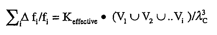
where λc is the wavelength of the central frequency. - Keffective is a constant related to the minimum volume occupied by the different excited modes taking into account the fact that the modes share a part of the volume. The different frequencies fi must be very close in order to have nearly overlapping bandwidths.
- Kphysical or Kobserved is defined by the structural volume V of the antenna and the overall antenna bandwidth:

- Kphysical or Kobserved is the most important K factor since it takes into account the real physical parameters and the usable bandwidth. Kphysical is also referred to as Kobserved since it is the only K factor that can be calculated experimentally. In order to have the modes confined within the physical volume of the antenna, Kphysical must be lower than Keffective. However these K factors are often nearly equal. The best and ideal case is obtained when Kphysical is approximately equal to Keffective and is also approximately equal to the smallest Kmodal. It should be noted that confining the modes inside the antenna is important in order to have a well-isolated antenna.
- One of the conclusions from the above calculations is that it is important to have the modes share as much volume as possible in order to have the different modes enclosed in the smallest volume possible.
- For a plurality of radiating modes i,
Figure 2 shows the observed return loss of a multiresonant structure. Different successive resonances occur at the frequencies f1,f2, fi,...fn. These peaks correspond to the different electromagnetic modes excited inside the structure.Figure 2 illustrates the relationship between the physical or observed K and the bandwidth over f1 to fn. - For a particular radiating mode with a resonant frequency at f1, we can consider the equivalent simplified circuit L1C1 shown in
Figure 3 . By neglecting the resistance in the equivalent circuit, the bandwidth of the antenna is simply a function of the radiation resistance. The circuit ofFigure 3 can be repeated to produce an equivalent circuit for a plurality of resonant frequencies. -
Figure 4 illustrates a multiresonant antenna represented by a plurality of LC circuits. At the frequency f1 only the circuit L1C1 is resonating. Physically, one part of the antenna structure resonates at each frequency within the covered spectrum. Again, neglecting real resistance of the structure, the bandwidth of each mode is a function of the radiation resistance. - As discussed above, in order to optimize the K factor, the antenna volume must be reused for the different resonant modes. One example of a multimode antenna utilizes a capacitively loaded microstrip type of antenna as the basic radiating structure. Modifications of this basic structure will be subsequently described. In all of the described examples, the elements of the multimode antenna structures have closely spaced resonant frequencies.
-
Figure 5 illustrates a single-mode capacitively loaded microstrip antenna. If we assume that the structure inFigure 5 can be modeled as a L1C1 circuit, then C1 corresponds to a fringing capacitance across gap g. Inductance L1 is mainly contributed by the loop designated by thenumeral 2. Another configuration of a capacitively loaded microstrip antenna is illustrated inFigure 6 . The capacitance in this case is a facing capacitance at the overlap designated by thenumeral 3. - A top plan view of a tri-mode antenna structure is shown in
Figure 7 . This structure comprises three sections corresponding to three different frequencies. The feed is placed inarea 7, which is similar to the feed arrangement used for the antennas ofFigure 5 andFigure 6 . This structure has three sets of fingers, 4/5, 8/9, and 10/11, configured similarly to the antenna ofFigure 5 . The different inductances are defined by the lengths offingers gaps -
Figure 8 is a perspective view of the antenna structure shown inFigure 7 . In this configuration, there is a separate capacitance and inductance for each of the frequencies. The different Li and Ci are set in order to have closely spaced frequencies fi. The slots S1 and S2 isolate the different parts of the antenna and therefore separate the frequencies of the antenna. This case shows that it is possible to partially reuse the volume of the antenna structure since thearea 7 associated with the feed is common to all of the modes. However, some portions of the volume are dedicated to only one of the frequencies. - Another solution for the reuse of the structure volume is depicted in
Figures 9a and 9b. Figure 9a is a variation of the basic structure shown inFigure 5 , whereasFigure 9b is a variation of the basic structure shown infigure 6 . In each case, slits 15 are placed near the sides of the antenna, along its length. The slits create a resonant structure at one frequency, but are electromagnetically transparent at a second characteristic frequency of the structure. The spacing of the resonant frequencies of the structure is mainly controlled by thedimensions figures 9a and 9b , two different antennas can be visualized - one by removing the material in theslits 15, which resonates at a first frequency, and the other by filling in the slits, which resonates at a second frequency. These two antennas in one clearly share the same volume. - An embodiment of a multifrequency antenna structure composed of overlapping structures is shown in
Figure 10 . Aplate 20 connected to anotherplate 21 is placed over a structure S like that shown inFigure 6 . The underlying structure S defines a capacitance C1 and an inductance L1 and is resonant at a frequency f1. Theplate 20 is placed at adistance 23 from one edge. Theplate 21 is placed at adistance 22 from the underlying structure, which defines a second capacitance C2. A second frequency f2 is characterized by the inductance L2 ofloop 24 and the capacitance C2 associated with gap 22 (the size of which is exaggerated in the figure). By optimizing C1, C2, L1 and L2 it is possible to achieve a set of two close frequencies that will indeed increase the K factor while reusing the same volume. In this case the volume V1 is included within the volume V2. It should be noted that f2 is not necessarily lower than f1. -
Figure 11 illustrates an extension of the structure shownFigure 10 in which several plates 20-21, 29-30, 31 and 32 have been superposed on an underlying structure S to create a plurality ofloops
This concept can be extended to an arbitrary number of stacked loops. -
Figure 12 illustrates an antenna having afirst structure 34 of the type shown inFigure 5 included within a secondsuch structure 33. The feeding point could be coupled to the end of eitherplate 35 orplate 36 or along any of the open edges. Here, the volume of one antenna is completely included in the volume of the other. -
Figure 13 illustrates another embodiment in which a plurality of structures share common parts and volumes. In this case, the loops associated with the characteristic inductances of the structures are numbered 37 and 38. This concept can be extended to more than two frequencies. The dimensions of the structures may be adjusted to achieve the desired capacitance values as previously described. It should be noted that the selected dimensions may give rise to parasitic frequencies and that these may be used in adjusting the overall antenna characteristics. - Another approach to making a multiresonant antenna is illustrated in
Figure 14 . Here, multiple antennas are combined in such a way that the coupling is low. The basic antenna element is the same as shown inFigure 6 : A set of such elements Fp1, Fp2, ...Fpi are stacked upon one another. One part of each Fpi is also a part of Fpi+1 and Fpi-1. The common parts will help to define the related capacitances Ci. The entire structure may have a common feeding point at Fp1 or separate feeding points may be located at Fp2...Fpi. - It is interesting to note that the width of the antenna structure does not have a critical influence on either the resonant frequency or the bandwidth. There is an optimum width for which the bandwidth of the basic element is at a maximum. Beyond this, the bandwidth does not increase as the width is increased.
- The limited effect of the antenna width on bandwidth allows consideration of the structure shown in
Figures 15a-b , which nests the individual antenna elements in both the vertical and horizontal directions. This allows more freedom in organizing the capacitive and inductive loading. This arrangement provides for the total inclusion of the inner antenna elements within the overall antenna volume, each element sharing a common ground. At different frequencies, only one element is resonating. -
Figure 16 illustrates an antenna structure comprising an array of elements, each of the general type shown inFigure 6 , having a drivenelement 40 and adjacent parasitic elements 41-43. Impedance matching of this structure is illustrated by the Smith chart shown inFigure 17 . The largeouter loop 50 corresponds to the main drivenelement 40, whereas the smaller loops 51-53 correspond to the parasitic elements. This is a representation of a non-optimized structure. Various adjustments can be made to the antenna elements to influence the positions of the loops on the Smith chart. The smaller loops may be gathered in the same area in order to obtain a constant impedance within the overall frequency range. - In the case of a typical 50 ohm connection, an optimized structure will have all of the loops gathered approximately in the center of the Smith chart as shown in
Figure 18 . In order to gather the loops in the center of the Smith chart (or wherever it is desired to place them), the dimensions of the individual antenna elements are adjusted, keeping in mind that each loop corresponds to one element. -
Figure 19 illustrates a single element, such as 41, of the antenna structure shown inFigure 16 . By reducing thedimension 1, the corresponding loop rotates clockwise on the Smith chart. By adjusting the length of the parasitic elements, all of the different loops can be gathered. Then, if necessary, the group of loops can be rotated back in the counter-clockwise direction on the Smith chart by reducing the length of the main driven element. - In order to optimize the bandwidth of the antenna structure, the main loop must have a large enough diameter. With reference to
Figure 20 , the diameter of the main loop is controlled by the amount of coupling between each element and its neighbor, which is determined by the distance dl between the adjacent elements. The amount of coupling is also controlled by the width of the elements. The narrower the elements are, the closer the elements can be in order to keep the same loop diameter. The ultimate size reduction is obtained when each element comprises a single wire. Furthermore, the elements can also be placed closer together by making thegap 45 smaller. - Finally, the main loop may be centered on the Smith chart by adjusting the location of the antenna feed on the main driven element. Referring to
Figure 21 , impedance matching of the antenna structure is optimized by adjusting the dimension If. By increasing If, the diameter of the main loop is increased. In this way, the small loops can be centered at the desired location on the Smith chart. -
Figure 22 illustrates a polarized multi-resonant antenna structure in which polarization diversity is achieved through the use of two interleaved arrays of antenna elements. In the case illustrated, the two arrays are arranged orthogonally to provide orthogonal polarization. The two arrays may be interconnected in various ways or they may be totally separated. It is easiest to have the arrays make contact where they cross, otherwise the manufacturing is more difficult. However it is not necessary that the arrays contact one another, and, in some cases, isolating the array elements from each other can be used for adjusting the impedance matching characteristics of the antenna. In any case, it is always possible to match the antenna by adjusting the various dimensions of the array elements as discussed earlier. - The use of one- or two-dimensional arrays of antenna elements allows the antenna structure to be co-located on a circuit board with other electronic components. The individual array elements can be placed between components mounted on the board. The electronic behavior of the components may be slightly affected by the presence of the radiating elements, but this can be determined through EMC studies and appropriate corrective measures, such as shielding of sensitive components, may be implemented. However, the electronic components will generally not perturb the electromagnetic field and will therefore not change the characteristics of the antenna.
- The two-dimensional array shown in
Figure 22 can be extrapolated to other array designs as illustrated inFigures 23a-d . The elements of the array can be arranged in various configurations to achieve spatial and/or polarization diversity. Other configurations in addition to those shown inFigures 23a-d are possible. In each case, the elements of the array may be interconnected in various ways or may be electrically isolated from one another. In addition, the individual elements may or may not be shorted to ground. All of these design parameters, including those previously discussed, permit the design of an antenna structure having the desired electromagnetic characteristics. - The design of an antenna structure must, of course, take into account manufacturing considerations, the objective being to achieve an antenna with both high efficiency and a low manufacturing cost. In achieving this objective, the problem of loss maybe a big issue. The electric field inside the capacitive part of the antenna is very high. Therefore, no material should be in between the two metallic layers.
- A first solution, as illustrated in
Figure 24 , utilizes an antenna element consisting of twowires Figure 24 shows a simple solution configured like a conventional surface mounted resistor. The wires are secured within a plastichollow cylinder 62 and the protruding wires are then soldered to the ground. - A second solution, as illustrated in
Figures 25a-b , utilizes an antenna element constructed as a printed circuit. Each element is printed on a very thin, low-loss dielectric substrate in order to achieve good efficiency. The printed circuit element is then placed vertically on the ground.
Figure 25a shows a simple two-arm element.Figure 25b shows a similar two-arm element with the ground printed on the substrate. - The parasitic elements of the antenna array need not be limited to the basic two-wire design shown in
Figures 5 and6 and in the later described structures based on these elements. Referring toFigure 26 , the parasitic elements may instead have a spiral configuration. The resonant frequency of the spiral element will be a function of the number of turns. It should be noted that when such a spiral element is coupled to a driven element having the configuration shown inFigure 5 orFigure 6 , the capacitive coupling is reduced since the driven element acts as a dipole, whereas the spiral element acts as a quadrupole. - It will be recognized that the above-described invention may be embodied in other specific forms without departing from the spirit or essential characteristics of the disclosure. Thus, it is understood that the invention is not to be limited by the foregoing illustrative details, but rather is to be defined by the appended claims.
Claims (24)
- An antenna comprising:a ground plane;a first conductor extending longitudinally parallel to the ground plane having a first end electrically connected to the ground plane and a second end;a second conductor extending longitudinally parallel to the ground plane having a first end electrically connected to the ground plane and a second end spaced apart from the second end of the first conductor;an antenna feed coupled to the first conductor;wherein at least one of the first and second conductors is slotted longitudinally.
- The antenna of claim 1 wherein the first and second conductors are equidistant from the ground plane.
- The antenna of claim 1 wherein the first and second conductors are not equidistant from the ground plane.
- The antenna of claim 3 wherein the respective second ends of the first and second conductors overlap.
- The antenna of claim 4 further comprising a third conductor extending longitudinally parallel to the ground plane having a first end electrically connected to the first conductor and a second end overlapping the second end of the second conductor.
- The antenna of claim 5 further comprising a fourth conductor extending longitudinally parallel to the ground plane having a first end electrically connected to the second conductor and a second end overlapping the second end of the third conductor.
- The antenna of claim 6 wherein the first end of the fourth conductor is aligned longitudinally with the first end of the second conductor.
- The antenna of claim 1 wherein both of the first and second conductors are slotted to define a plurality of parallel radiating elements, each comprising a portion of the first conductor and a corresponding portion of the second conductor, and wherein each portion of the first conductor has a respective second end spaced apart from a second end of a respective portion of the second conductor defining a gap for the respective radiating element.
- The antenna of claim 8 wherein the gap of at least one of the radiating elements is displaced longitudinally from the gap of another radiating element.
- The antenna of claim 1 wherein the slotted conductor comprises a central portion extending from the first end of the conductor toward the second end of the conductor and a pair of outboard fingers extending longitudinally from the second end of the conductor toward the first end of the conductor.
- The antenna of claim 9 wherein the respective second ends of the first and second conductors overlap.
- An antenna comprising:a ground plane;a first conductor extending longitudinally parallel to the ground plane having a first end electrically connected to the ground plane and a second end;a second conductor extending longitudinally parallel to the ground plane having a first end electrically connected to the ground plane and a second end spaced apart from the second end of the first conductor;a third conductor extending longitudinally parallel to the ground plane having a first end electrically connected to the ground plane and a second end spaced apart from the second ends of the first and second conductors;a fourth conductor extending longitudinally parallel to the ground plane having a first end electrically connected to the ground plane and a second end spaced apart from the second ends of the first, second and third conductors; andan antenna feed coupled to at least one of the first and third conductors.
- The antenna of claim 12 wherein the first and third conductors are in a stacked relationship and wherein the second and fourth conductors are in a stacked relationship.
- An antenna comprising
a ground plane;
a first conductor extending longitudinally parallel to the ground plane having a first end electrically connected to the ground plane and a second end;
a second conductor extending longitudinally parallel to the ground plane having a first end electrically connected to the ground plane and a second end overlapping the second end of the first conductor;
a third conductor extending longitudinally parallel to the ground plane having a first end electrically connected to the ground plane and a second end overlapping the second conductor;
an antenna feed coupled to the first conductor. - An antenna comprising:a ground plane;an array of radiating elements, each of the radiating elements having a first conductor extending longitudinally parallel to the ground plane having a first end electrically connected to the ground plane and a second end, and a second conductor extending longitudinally parallel to the ground plane having a first end electrically connected to the ground plane and a second end spaced apart from the second end of the first conductor;an antenna feed coupled to the first conductor of at least one of the radiating elements.
- The antenna of claim 15 wherein the first and second conductors of each radiating element are not equidistant from the ground plane.
- The antenna of claim 16 wherein the respective second ends of the first and second conductors overlap.
- The antenna of claim 15 wherein the radiating elements are arranged in a parallel array.
- The antenna of claim 15 wherein the radiating elements are arranged in a first parallel subarray and a second parallel subarray orthogonal to the first subarray.
- The antenna of claim 15 wherein the radiating elements are arranged in a non-parallel array.
- The antenna of claim 15 further comprising a radiating element having a conductor with a spiral configuration.
- The antenna of claim 15 wherein the radiating elements comprise first and second conductive wires held in a spaced apart relationship.
- The antenna of claim 22 wherein the first and second conductive wires are held in the spaced apart relationship by a non-conductive tubular element.
- The antenna of claim 15 wherein the radiating elements comprise printed circuit boards.
Applications Claiming Priority (2)
| Application Number | Priority Date | Filing Date | Title |
|---|---|---|---|
| US09/892,928 US6456243B1 (en) | 2001-06-26 | 2001-06-26 | Multi frequency magnetic dipole antenna structures and methods of reusing the volume of an antenna |
| EP02742309A EP1413002A2 (en) | 2001-06-26 | 2002-06-24 | Multi frequency magnetic dipole antenna structures and methods of reusing the volume of an antenna |
Related Parent Applications (1)
| Application Number | Title | Priority Date | Filing Date |
|---|---|---|---|
| EP02742309A Division EP1413002A2 (en) | 2001-06-26 | 2002-06-24 | Multi frequency magnetic dipole antenna structures and methods of reusing the volume of an antenna |
Publications (2)
| Publication Number | Publication Date |
|---|---|
| EP1959518A2 true EP1959518A2 (en) | 2008-08-20 |
| EP1959518A3 EP1959518A3 (en) | 2008-11-05 |
Family
ID=25400726
Family Applications (2)
| Application Number | Title | Priority Date | Filing Date |
|---|---|---|---|
| EP08003137A Withdrawn EP1959518A3 (en) | 2001-06-26 | 2002-06-24 | Multifrequency magnetic dipole antenna and methods for re-using the volume of an antenna |
| EP02742309A Ceased EP1413002A2 (en) | 2001-06-26 | 2002-06-24 | Multi frequency magnetic dipole antenna structures and methods of reusing the volume of an antenna |
Family Applications After (1)
| Application Number | Title | Priority Date | Filing Date |
|---|---|---|---|
| EP02742309A Ceased EP1413002A2 (en) | 2001-06-26 | 2002-06-24 | Multi frequency magnetic dipole antenna structures and methods of reusing the volume of an antenna |
Country Status (5)
| Country | Link |
|---|---|
| US (2) | US6456243B1 (en) |
| EP (2) | EP1959518A3 (en) |
| CN (1) | CN100433454C (en) |
| AU (1) | AU2002315455A1 (en) |
| WO (1) | WO2003003503A2 (en) |
Cited By (3)
| Publication number | Priority date | Publication date | Assignee | Title |
|---|---|---|---|---|
| WO2010042846A3 (en) * | 2008-10-10 | 2010-07-08 | Lhc2 Inc | Spiraling surface antenna |
| WO2010085706A2 (en) * | 2009-01-23 | 2010-07-29 | Lhc2 Inc | Compact circularly polarized omni-directional antenna |
| US7948440B1 (en) | 2006-09-30 | 2011-05-24 | LHC2 Inc. | Horizontally-polarized omni-directional antenna |
Families Citing this family (78)
| Publication number | Priority date | Publication date | Assignee | Title |
|---|---|---|---|---|
| MXPA02003084A (en) | 1999-09-20 | 2003-08-20 | Fractus Sa | Multilevel antennae. |
| JP2002353731A (en) * | 2001-05-15 | 2002-12-06 | Z-Com Inc | Inverted-f antenna and its manufacturing method |
| US7339531B2 (en) * | 2001-06-26 | 2008-03-04 | Ethertronics, Inc. | Multi frequency magnetic dipole antenna structures and method of reusing the volume of an antenna |
| US6573867B1 (en) * | 2002-02-15 | 2003-06-03 | Ethertronics, Inc. | Small embedded multi frequency antenna for portable wireless communications |
| US6717551B1 (en) * | 2002-11-12 | 2004-04-06 | Ethertronics, Inc. | Low-profile, multi-frequency, multi-band, magnetic dipole antenna |
| US6943730B2 (en) * | 2002-04-25 | 2005-09-13 | Ethertronics Inc. | Low-profile, multi-frequency, multi-band, capacitively loaded magnetic dipole antenna |
| US6744410B2 (en) * | 2002-05-31 | 2004-06-01 | Ethertronics, Inc. | Multi-band, low-profile, capacitively loaded antennas with integrated filters |
| AU2003223717A1 (en) * | 2002-04-25 | 2003-11-10 | Ethertronics, Inc. | Low-profile, multi-frequency, multi-band, capacitively loaded magnetic dipole antenna |
| TW542416U (en) * | 2002-06-20 | 2003-07-11 | Hon Hai Prec Ind Co Ltd | Dual-band antenna |
| DE10231961B3 (en) * | 2002-07-15 | 2004-02-12 | Kathrein-Werke Kg | Low-profile dual or multi-band antenna, especially for motor vehicles |
| WO2004025778A1 (en) | 2002-09-10 | 2004-03-25 | Fractus, S.A. | Coupled multiband antennas |
| EP1579529A4 (en) * | 2002-12-17 | 2007-09-19 | Ethertronics Inc | Antennas with reduced space and improved performance |
| US20040233113A1 (en) * | 2003-05-24 | 2004-11-25 | Laurent Desclos | Multi band low frequency phone and antenna design |
| US6850200B2 (en) * | 2003-06-13 | 2005-02-01 | Motorola, Inc. | Compact PIFA antenna for automated manufacturing |
| KR100586938B1 (en) * | 2003-09-19 | 2006-06-07 | 삼성전기주식회사 | Internal diversity antenna |
| US7408517B1 (en) | 2004-09-14 | 2008-08-05 | Kyocera Wireless Corp. | Tunable capacitively-loaded magnetic dipole antenna |
| US7239290B2 (en) * | 2004-09-14 | 2007-07-03 | Kyocera Wireless Corp. | Systems and methods for a capacitively-loaded loop antenna |
| GB0501938D0 (en) * | 2005-02-01 | 2005-03-09 | Antenova Ltd | Balanced-unbalanced antennas for cellular radio handsets, PDAs etc |
| TWI318809B (en) * | 2005-05-23 | 2009-12-21 | Hon Hai Prec Ind Co Ltd | Multi-frequency antenna |
| US7274338B2 (en) * | 2005-10-12 | 2007-09-25 | Kyocera Corporation | Meander line capacitively-loaded magnetic dipole antenna |
| US7427965B2 (en) * | 2005-10-12 | 2008-09-23 | Kyocera Corporation | Multiple band capacitively-loaded loop antenna |
| US7696932B2 (en) * | 2006-04-03 | 2010-04-13 | Ethertronics | Antenna configured for low frequency applications |
| US7663556B2 (en) * | 2006-04-03 | 2010-02-16 | Ethertronics, Inc. | Antenna configured for low frequency application |
| US8738103B2 (en) | 2006-07-18 | 2014-05-27 | Fractus, S.A. | Multiple-body-configuration multimedia and smartphone multifunction wireless devices |
| US7911402B2 (en) * | 2008-03-05 | 2011-03-22 | Ethertronics, Inc. | Antenna and method for steering antenna beam direction |
| US7932869B2 (en) * | 2007-08-17 | 2011-04-26 | Ethertronics, Inc. | Antenna with volume of material |
| US9941588B2 (en) | 2007-08-20 | 2018-04-10 | Ethertronics, Inc. | Antenna with multiple coupled regions |
| US7830320B2 (en) * | 2007-08-20 | 2010-11-09 | Ethertronics, Inc. | Antenna with active elements |
| US20090102738A1 (en) * | 2007-10-19 | 2009-04-23 | Andrew Corporation | Antenna Having Unitary Radiating And Grounding Structure |
| US8121821B1 (en) | 2007-12-19 | 2012-02-21 | The United States Of America As Represented By The Secretary Of The Navy | Quasi-static design approach for low Q factor electrically small antennas |
| US8368156B1 (en) | 2007-12-19 | 2013-02-05 | The United States Of America As Represented By The Secretary Of The Navy | Dipole moment term for an electrically small antenna |
| US9748637B2 (en) | 2008-03-05 | 2017-08-29 | Ethertronics, Inc. | Antenna and method for steering antenna beam direction for wifi applications |
| US10033097B2 (en) | 2008-03-05 | 2018-07-24 | Ethertronics, Inc. | Integrated antenna beam steering system |
| US9761940B2 (en) | 2008-03-05 | 2017-09-12 | Ethertronics, Inc. | Modal adaptive antenna using reference signal LTE protocol |
| US9917359B2 (en) | 2008-03-05 | 2018-03-13 | Ethertronics, Inc. | Repeater with multimode antenna |
| JP5650646B2 (en) * | 2008-09-12 | 2015-01-07 | インフィニット パワー ソリューションズ, インコーポレイテッド | Energy device with integral conductive surface for data communication via electromagnetic energy and method for data communication via electromagnetic energy |
| TW201021286A (en) * | 2008-11-18 | 2010-06-01 | Unictron Technologies Corp | Miniature antenna |
| TWI418090B (en) * | 2009-03-26 | 2013-12-01 | Walsin Technology Corp | Ceramic wafer antenna |
| KR101225038B1 (en) * | 2009-06-16 | 2013-01-23 | 전북대학교산학협력단 | Tag antenna using microstrip lines and manufacturing method thereof, RFID tag |
| FI20095965A0 (en) | 2009-09-18 | 2009-09-18 | Valtion Teknillinen | Antenna construction e.g. for an RFID transponder |
| US8228243B1 (en) * | 2009-09-30 | 2012-07-24 | The United States Of America As Represented By The Secretary Of The Navy | Parallel plate antenna |
| TWM378495U (en) * | 2009-10-23 | 2010-04-11 | Unictron Technologies Corp | Miniature multi-frequency antenna |
| WO2011050845A1 (en) * | 2009-10-29 | 2011-05-05 | Laird Technologies Ab | A metal cover for a radio communication device |
| EP2355241A1 (en) * | 2010-02-02 | 2011-08-10 | Laird Technologies AB | An antenna device for a radio communication device |
| EP2355242A1 (en) * | 2010-02-02 | 2011-08-10 | Laird Technologies AB | An antenna device for a radio communication device |
| EP2387100B1 (en) * | 2010-04-29 | 2012-12-05 | Laird Technologies AB | A metal cover for a radio communication device |
| GB2500136B (en) | 2010-10-15 | 2015-02-18 | Microsoft Corp | Parasitic folded loop antenna |
| EP2469645B1 (en) * | 2010-12-22 | 2013-05-15 | Laird Technologies AB | An antenna arrangement for a portable radio communication device having a metal casing |
| EP2469644A1 (en) * | 2010-12-22 | 2012-06-27 | Laird Technologies AB | An antenna arrangement for a portable radio communication device |
| US8581783B2 (en) | 2011-03-10 | 2013-11-12 | Teledyne Scientific & Imaging, Llc | Metamaterial-based direction-finding antenna systems |
| US8963794B2 (en) | 2011-08-23 | 2015-02-24 | Apple Inc. | Distributed loop antennas |
| US9349091B2 (en) | 2011-11-04 | 2016-05-24 | Teknologian Tutkimuskeskus Vtt | Antenna construction, for example for an RFID transponder system |
| US8890766B2 (en) * | 2011-12-01 | 2014-11-18 | Sony Corporation | Low profile multi-band antennas and related wireless communications devices |
| US9431711B2 (en) * | 2012-08-31 | 2016-08-30 | Shure Incorporated | Broadband multi-strip patch antenna |
| WO2014184614A1 (en) * | 2013-05-13 | 2014-11-20 | Freescale Semiconductor, Inc. | Method and apparatus for enabling temporal alignment of debug information |
| JP6478510B2 (en) | 2013-08-20 | 2019-03-06 | キヤノン株式会社 | antenna |
| JP6225644B2 (en) * | 2013-11-01 | 2017-11-08 | セイコーエプソン株式会社 | Antenna, communication device and electronic device |
| CN104916913B (en) * | 2015-06-11 | 2017-11-07 | 华南理工大学 | A kind of omnidirectional antenna of the frequency horizontal polarization of knife-edge three |
| TWI606638B (en) | 2015-12-30 | 2017-11-21 | 連展科技股份有限公司 | Laminated integrated antenna |
| CN106329102A (en) * | 2016-08-31 | 2017-01-11 | 中国电子科技集团公司第三十六研究所 | Novel LTCC interdigital antenna |
| JP6776847B2 (en) * | 2016-11-24 | 2020-10-28 | 富士通株式会社 | Loop antennas and electronic devices |
| US10276916B2 (en) * | 2016-12-19 | 2019-04-30 | Panasonic Intellectual Property Management Co., Ltd. | Antenna device |
| US10522915B2 (en) * | 2017-02-01 | 2019-12-31 | Shure Acquisition Holdings, Inc. | Multi-band slotted planar antenna |
| WO2019142677A1 (en) * | 2018-01-22 | 2019-07-25 | 京セラ株式会社 | Antenna, wireless communication device, wireless communication system, vehicle, motorcycle, and mobile body |
| JP7084430B2 (en) * | 2018-01-22 | 2022-06-14 | 京セラ株式会社 | Antennas, wireless communication equipment, wheels, tire pressure monitoring systems, and vehicles |
| WO2019142937A1 (en) * | 2018-01-22 | 2019-07-25 | 京セラ株式会社 | Relay device |
| JP6957760B2 (en) * | 2018-08-24 | 2021-11-02 | 京セラ株式会社 | Structures, antennas, wireless communication modules, and wireless communication equipment |
| US11831082B2 (en) | 2018-08-24 | 2023-11-28 | Kyocera Corporation | Structure, antenna, wireless communication module, and wireless communication device |
| US11527820B2 (en) * | 2018-08-24 | 2022-12-13 | Kyocera Corporation | Structure, antenna, wireless communication module, and wireless communication device |
| WO2020045395A1 (en) * | 2018-08-27 | 2020-03-05 | 京セラ株式会社 | Resonant structure, antenna, wireless communication module, and wireless communication device |
| JP7361601B2 (en) * | 2019-12-26 | 2023-10-16 | 京セラ株式会社 | Antenna units, wireless communication modules and wireless communication equipment |
| US11735826B2 (en) | 2020-05-28 | 2023-08-22 | KYOCERA AVX Components (San Diego), Inc. | Modal antenna system including closed-loop parasitic element |
| US11881618B2 (en) | 2020-07-10 | 2024-01-23 | KYOCERA AVX Components (San Diego), Inc. | Antenna system with coupled region |
| US11742580B2 (en) | 2020-07-28 | 2023-08-29 | KYOCERA AVX Components (San Diego), Inc. | Multifeed antenna system with capacitively coupled feed elements |
| EP4238182A1 (en) | 2021-01-07 | 2023-09-06 | Kyocera Avx Components (San Diego), Inc. | Circularly polarized array antenna for millimeter wave communications |
| US11936119B2 (en) | 2021-01-29 | 2024-03-19 | KYOCERA AVX Components (San Diego), Inc. | Isolated magnetic dipole antennas having angled edges for improved tuning |
| CN118137128A (en) * | 2021-02-10 | 2024-06-04 | 华为技术有限公司 | Antenna and electronic equipment |
| TWI812125B (en) * | 2022-03-28 | 2023-08-11 | 詠業科技股份有限公司 | Antenna device and antenna equipment with touch function |
Citations (1)
| Publication number | Priority date | Publication date | Assignee | Title |
|---|---|---|---|---|
| WO1998038694A1 (en) * | 1997-02-25 | 1998-09-03 | Pates Technology Patentverwertungsgesellschaft Für Satelliten- Und Moderne Informationstechnologien Mbh | Resonant antenna |
Family Cites Families (78)
| Publication number | Priority date | Publication date | Assignee | Title |
|---|---|---|---|---|
| US4328502A (en) | 1965-06-21 | 1982-05-04 | The United States Of America As Represented By The Secretary Of The Navy | Continuous slot antennas |
| US3648172A (en) | 1968-10-02 | 1972-03-07 | Sumitomo Electric Industries | Circular leaky waveguide train communication system |
| US3827053A (en) * | 1970-07-23 | 1974-07-30 | E Willie | Antenna with large capacitive termination and low noise input circuit |
| US3721990A (en) | 1971-12-27 | 1973-03-20 | Rca Corp | Physically small combined loop and dipole all channel television antenna system |
| US3845487A (en) | 1972-09-26 | 1974-10-29 | U Lammers | Radio direction finding system |
| US4218682A (en) * | 1979-06-22 | 1980-08-19 | Nasa | Multiple band circularly polarized microstrip antenna |
| JPS5612102A (en) * | 1979-07-11 | 1981-02-06 | Nippon Telegr & Teleph Corp <Ntt> | Broad-band reversed-l-shaped antenna |
| US4450449A (en) | 1982-02-25 | 1984-05-22 | Honeywell Inc. | Patch array antenna |
| US4684952A (en) * | 1982-09-24 | 1987-08-04 | Ball Corporation | Microstrip reflectarray for satellite communication and radar cross-section enhancement or reduction |
| US4749996A (en) * | 1983-08-29 | 1988-06-07 | Allied-Signal Inc. | Double tuned, coupled microstrip antenna |
| US4598276A (en) * | 1983-11-16 | 1986-07-01 | Minnesota Mining And Manufacturing Company | Distributed capacitance LC resonant circuit |
| US5173711A (en) * | 1989-11-27 | 1992-12-22 | Kokusai Denshin Denwa Kabushiki Kaisha | Microstrip antenna for two-frequency separate-feeding type for circularly polarized waves |
| US5087922A (en) * | 1989-12-08 | 1992-02-11 | Hughes Aircraft Company | Multi-frequency band phased array antenna using coplanar dipole array with multiple feed ports |
| US5220335A (en) * | 1990-03-30 | 1993-06-15 | The United States Of America As Represented By The Administrator Of The National Aeronautics And Space Administration | Planar microstrip Yagi antenna array |
| US5245745A (en) | 1990-07-11 | 1993-09-21 | Ball Corporation | Method of making a thick-film patch antenna structure |
| US5184144A (en) | 1990-09-25 | 1993-02-02 | Chu Associates, Inc. | Ogival cross-section combined microwave waveguide for reflector antenna feed and spar support therefor |
| FR2669776B1 (en) | 1990-11-23 | 1993-01-22 | Thomson Csf | SLOTTED MICROWAVE ANTENNA WITH LOW THICKNESS STRUCTURE. |
| US5309164A (en) | 1992-04-13 | 1994-05-03 | Andrew Corporation | Patch-type microwave antenna having wide bandwidth and low cross-pol |
| DK168780B1 (en) * | 1992-04-15 | 1994-06-06 | Celwave R F A S | Antenna system and method of manufacture thereof |
| JP3239435B2 (en) * | 1992-04-24 | 2001-12-17 | ソニー株式会社 | Planar antenna |
| JP3457351B2 (en) | 1992-09-30 | 2003-10-14 | 株式会社東芝 | Portable wireless devices |
| FR2699740B1 (en) * | 1992-12-23 | 1995-03-03 | Patrice Brachat | Broadband antenna with reduced overall dimensions, and corresponding transmitting and / or receiving device. |
| EP0954050A1 (en) * | 1993-05-27 | 1999-11-03 | Griffith University | Antennas for use in portable communications devices |
| US5450090A (en) | 1994-07-20 | 1995-09-12 | The Charles Stark Draper Laboratory, Inc. | Multilayer miniaturized microstrip antenna |
| FR2727250A1 (en) | 1994-11-22 | 1996-05-24 | Brachat Patrice | MONOPOLY BROADBAND ANTENNA IN UNIPLANAR PRINTED TECHNOLOGY AND TRANSMITTING AND / OR RECEIVING DEVICE INCORPORATING SUCH ANTENNA |
| US5790080A (en) | 1995-02-17 | 1998-08-04 | Lockheed Sanders, Inc. | Meander line loaded antenna |
| US5781158A (en) * | 1995-04-25 | 1998-07-14 | Young Hoek Ko | Electric/magnetic microstrip antenna |
| US5627550A (en) * | 1995-06-15 | 1997-05-06 | Nokia Mobile Phones Ltd. | Wideband double C-patch antenna including gap-coupled parasitic elements |
| GB2303968B (en) * | 1995-08-03 | 1999-11-10 | Nokia Mobile Phones Ltd | Antenna |
| JP3169325B2 (en) * | 1995-08-14 | 2001-05-21 | 東洋通信機株式会社 | Array antenna |
| JP3319268B2 (en) * | 1996-02-13 | 2002-08-26 | 株式会社村田製作所 | Surface mount antenna and communication device using the same |
| EP0795926B1 (en) | 1996-03-13 | 2002-12-11 | Ascom Systec AG | Flat, three-dimensional antenna |
| US5726666A (en) | 1996-04-02 | 1998-03-10 | Ems Technologies, Inc. | Omnidirectional antenna with single feedpoint |
| FR2748162B1 (en) | 1996-04-24 | 1998-07-24 | Brachat Patrice | COMPACT PRINTED ANTENNA FOR LOW ELEVATION RADIATION |
| SE507077C2 (en) | 1996-05-17 | 1998-03-23 | Allgon Ab | Antenna device for a portable radio communication device |
| JP3296189B2 (en) * | 1996-06-03 | 2002-06-24 | 三菱電機株式会社 | Antenna device |
| US5764190A (en) | 1996-07-15 | 1998-06-09 | The Hong Kong University Of Science & Technology | Capacitively loaded PIFA |
| FR2752646B1 (en) | 1996-08-21 | 1998-11-13 | France Telecom | FLAT PRINTED ANTENNA WITH SHORT-LAYERED ELEMENTS |
| DE19740254A1 (en) | 1996-10-16 | 1998-04-23 | Lindenmeier Heinz | Radio antenna arrangement e.g. for GSM |
| US5754143A (en) | 1996-10-29 | 1998-05-19 | Southwest Research Institute | Switch-tuned meandered-slot antenna |
| US5900843A (en) | 1997-03-18 | 1999-05-04 | Raytheon Company | Airborne VHF antennas |
| FI110395B (en) * | 1997-03-25 | 2003-01-15 | Nokia Corp | Broadband antenna is provided with short-circuited microstrips |
| US6114996A (en) * | 1997-03-31 | 2000-09-05 | Qualcomm Incorporated | Increased bandwidth patch antenna |
| US6008762A (en) | 1997-03-31 | 1999-12-28 | Qualcomm Incorporated | Folded quarter-wave patch antenna |
| US6057802A (en) * | 1997-06-30 | 2000-05-02 | Virginia Tech Intellectual Properties, Inc. | Trimmed foursquare antenna radiating element |
| US6046707A (en) * | 1997-07-02 | 2000-04-04 | Kyocera America, Inc. | Ceramic multilayer helical antenna for portable radio or microwave communication apparatus |
| SE518818C2 (en) | 1997-11-14 | 2002-11-26 | Moteco Ab | Antenna device for dual frequency bands |
| FR2772518B1 (en) * | 1997-12-11 | 2000-01-07 | Alsthom Cge Alcatel | SHORT-CIRCUIT ANTENNA MADE ACCORDING TO MICRO-TAPE TECHNIQUE AND DEVICE INCLUDING THIS ANTENNA |
| GB2333902B (en) | 1998-01-31 | 2002-10-23 | Nec Technologies | Directive antenna for mobile telephones |
| US6157348A (en) | 1998-02-04 | 2000-12-05 | Antenex, Inc. | Low profile antenna |
| US6184833B1 (en) * | 1998-02-23 | 2001-02-06 | Qualcomm, Inc. | Dual strip antenna |
| JP3252786B2 (en) * | 1998-02-24 | 2002-02-04 | 株式会社村田製作所 | Antenna device and wireless device using the same |
| JP2000031735A (en) * | 1998-03-24 | 2000-01-28 | Ddi Corp | Adaptive array antenna device |
| SE9804498D0 (en) * | 1998-04-02 | 1998-12-22 | Allgon Ab | Wide band antenna means incorporating a radiating structure having a band shape |
| US6140965A (en) | 1998-05-06 | 2000-10-31 | Northrop Grumman Corporation | Broad band patch antenna |
| SE512439C2 (en) | 1998-06-26 | 2000-03-20 | Allgon Ab | Dual band antenna |
| JP2000068736A (en) * | 1998-08-21 | 2000-03-03 | Toshiba Corp | Multi-frequency antenna |
| US6121932A (en) | 1998-11-03 | 2000-09-19 | Motorola, Inc. | Microstrip antenna and method of forming same |
| US6181281B1 (en) * | 1998-11-25 | 2001-01-30 | Nec Corporation | Single- and dual-mode patch antennas |
| US6381471B1 (en) | 1999-06-30 | 2002-04-30 | Vladimir A. Dvorkin | Dual band radio telephone with dedicated receive and transmit antennas |
| DE69941025D1 (en) * | 1999-07-09 | 2009-08-06 | Ipcom Gmbh & Co Kg | Two band radio |
| JP3788115B2 (en) * | 1999-07-23 | 2006-06-21 | 松下電器産業株式会社 | Method for manufacturing antenna device |
| TW431033B (en) * | 1999-09-03 | 2001-04-21 | Ind Tech Res Inst | Twin-notch loaded type microstrip antenna |
| WO2001020714A1 (en) * | 1999-09-10 | 2001-03-22 | Galtronics Ltd. | Broadband or multi-band planar antenna |
| US6417807B1 (en) * | 2001-04-27 | 2002-07-09 | Hrl Laboratories, Llc | Optically controlled RF MEMS switch array for reconfigurable broadband reflective antennas |
| US6310584B1 (en) * | 2000-01-18 | 2001-10-30 | Xircom Wireless, Inc. | Low profile high polarization purity dual-polarized antennas |
| US6529749B1 (en) * | 2000-05-22 | 2003-03-04 | Ericsson Inc. | Convertible dipole/inverted-F antennas and wireless communicators incorporating the same |
| US6483481B1 (en) * | 2000-11-14 | 2002-11-19 | Hrl Laboratories, Llc | Textured surface having high electromagnetic impedance in multiple frequency bands |
| US6362789B1 (en) * | 2000-12-22 | 2002-03-26 | Rangestar Wireless, Inc. | Dual band wideband adjustable antenna assembly |
| US6339409B1 (en) * | 2001-01-24 | 2002-01-15 | Southwest Research Institute | Wide bandwidth multi-mode antenna |
| US6567053B1 (en) * | 2001-02-12 | 2003-05-20 | Eli Yablonovitch | Magnetic dipole antenna structure and method |
| US6323810B1 (en) * | 2001-03-06 | 2001-11-27 | Ethertronics, Inc. | Multimode grounded finger patch antenna |
| TW490885B (en) * | 2001-05-25 | 2002-06-11 | Chi Mei Comm Systems Inc | Broadband dual-band antenna |
| US6675461B1 (en) * | 2001-06-26 | 2004-01-13 | Ethertronics, Inc. | Method for manufacturing a magnetic dipole antenna |
| US6690327B2 (en) * | 2001-09-19 | 2004-02-10 | Etenna Corporation | Mechanically reconfigurable artificial magnetic conductor |
| US6646610B2 (en) * | 2001-12-21 | 2003-11-11 | Nokia Corporation | Antenna |
| US6639558B2 (en) * | 2002-02-06 | 2003-10-28 | Tyco Electronics Corp. | Multi frequency stacked patch antenna with improved frequency band isolation |
| US6573867B1 (en) * | 2002-02-15 | 2003-06-03 | Ethertronics, Inc. | Small embedded multi frequency antenna for portable wireless communications |
-
2001
- 2001-06-26 US US09/892,928 patent/US6456243B1/en not_active Expired - Lifetime
-
2002
- 2002-06-24 CN CNB028128206A patent/CN100433454C/en not_active Expired - Lifetime
- 2002-06-24 EP EP08003137A patent/EP1959518A3/en not_active Withdrawn
- 2002-06-24 AU AU2002315455A patent/AU2002315455A1/en not_active Abandoned
- 2002-06-24 EP EP02742309A patent/EP1413002A2/en not_active Ceased
- 2002-06-24 WO PCT/US2002/020242 patent/WO2003003503A2/en not_active Application Discontinuation
- 2002-09-23 US US10/253,016 patent/US7012568B2/en not_active Expired - Lifetime
Patent Citations (1)
| Publication number | Priority date | Publication date | Assignee | Title |
|---|---|---|---|---|
| WO1998038694A1 (en) * | 1997-02-25 | 1998-09-03 | Pates Technology Patentverwertungsgesellschaft Für Satelliten- Und Moderne Informationstechnologien Mbh | Resonant antenna |
Cited By (6)
| Publication number | Priority date | Publication date | Assignee | Title |
|---|---|---|---|---|
| US7948440B1 (en) | 2006-09-30 | 2011-05-24 | LHC2 Inc. | Horizontally-polarized omni-directional antenna |
| WO2010042846A3 (en) * | 2008-10-10 | 2010-07-08 | Lhc2 Inc | Spiraling surface antenna |
| US8570239B2 (en) | 2008-10-10 | 2013-10-29 | LHC2 Inc. | Spiraling surface antenna |
| WO2010085706A2 (en) * | 2009-01-23 | 2010-07-29 | Lhc2 Inc | Compact circularly polarized omni-directional antenna |
| WO2010085706A3 (en) * | 2009-01-23 | 2010-11-25 | Lhc2 Inc | Compact circularly polarized omni-directional antenna |
| US8203500B2 (en) | 2009-01-23 | 2012-06-19 | Lhc2 Inc | Compact circularly polarized omni-directional antenna |
Also Published As
| Publication number | Publication date |
|---|---|
| US20040027286A1 (en) | 2004-02-12 |
| EP1959518A3 (en) | 2008-11-05 |
| CN100433454C (en) | 2008-11-12 |
| WO2003003503A3 (en) | 2003-05-08 |
| US7012568B2 (en) | 2006-03-14 |
| AU2002315455A1 (en) | 2003-03-03 |
| EP1413002A2 (en) | 2004-04-28 |
| WO2003003503A2 (en) | 2003-01-09 |
| CN1520629A (en) | 2004-08-11 |
| US6456243B1 (en) | 2002-09-24 |
Similar Documents
| Publication | Publication Date | Title |
|---|---|---|
| US6456243B1 (en) | Multi frequency magnetic dipole antenna structures and methods of reusing the volume of an antenna | |
| KR101800910B1 (en) | Dielectric chip antennas | |
| US7071889B2 (en) | Low frequency enhanced frequency selective surface technology and applications | |
| EP1756908B1 (en) | Method and device for loading planar antennas | |
| JP3992077B2 (en) | Antenna structure and wireless communication device including the same | |
| US20110115584A1 (en) | Periodic structure | |
| US6819289B2 (en) | Chip antenna with parasitic elements | |
| US20140347226A1 (en) | Back face antenna for a computing device case | |
| JP2007049674A (en) | Antenna structure | |
| JP2004088218A (en) | Planar antenna | |
| JP2002319811A (en) | Plural resonance antenna | |
| US20040233111A1 (en) | Multi frequency magnetic dipole antenna structures and method of reusing the volume of an antenna | |
| KR20020071779A (en) | Antenna element | |
| JP2004336250A (en) | Antenna matching circuit, and mobile communication apparatus and dielectric antenna having the same | |
| JPS61196603A (en) | Antenna | |
| KR19990028387A (en) | Combined multi-segment helical antenna | |
| US6906667B1 (en) | Multi frequency magnetic dipole antenna structures for very low-profile antenna applications | |
| JP2001513283A (en) | Resonant antenna | |
| KR20100079243A (en) | Infinite wavelength antenna apparatus | |
| WO2015019100A1 (en) | Wide band array antenna | |
| JP2013530623A (en) | Antenna with planar conductive element | |
| WO2004013933A1 (en) | Low frequency enhanced frequency selective surface technology and applications | |
| KR101535641B1 (en) | Antenna apparatus for impedance matching from internal part | |
| KR100688648B1 (en) | Multi-band internal antenna using a short stub for mobile terminals | |
| US11387567B1 (en) | Multiband antenna with dipole resonant structures |
Legal Events
| Date | Code | Title | Description |
|---|---|---|---|
| PUAI | Public reference made under article 153(3) epc to a published international application that has entered the european phase |
Free format text: ORIGINAL CODE: 0009012 |
|
| AC | Divisional application: reference to earlier application |
Ref document number: 1413002 Country of ref document: EP Kind code of ref document: P |
|
| AK | Designated contracting states |
Kind code of ref document: A2 Designated state(s): AT BE CH CY DE DK ES FI FR GB GR IE IT LI LU MC NL PT SE TR |
|
| PUAL | Search report despatched |
Free format text: ORIGINAL CODE: 0009013 |
|
| AK | Designated contracting states |
Kind code of ref document: A3 Designated state(s): AT BE CH CY DE DK ES FI FR GB GR IE IT LI LU MC NL PT SE TR |
|
| 17P | Request for examination filed |
Effective date: 20090502 |
|
| 17Q | First examination report despatched |
Effective date: 20090608 |
|
| AKX | Designation fees paid |
Designated state(s): AT BE CH CY DE DK ES FI FR GB GR IE IT LI LU MC NL PT SE TR |
|
| STAA | Information on the status of an ep patent application or granted ep patent |
Free format text: STATUS: THE APPLICATION HAS BEEN WITHDRAWN |
|
| 18W | Application withdrawn |
Effective date: 20110825 |