EP1958981A2 - Barriere laminate, barrier film substrate, methods for producing them, and device - Google Patents
Barriere laminate, barrier film substrate, methods for producing them, and device Download PDFInfo
- Publication number
- EP1958981A2 EP1958981A2 EP08002713A EP08002713A EP1958981A2 EP 1958981 A2 EP1958981 A2 EP 1958981A2 EP 08002713 A EP08002713 A EP 08002713A EP 08002713 A EP08002713 A EP 08002713A EP 1958981 A2 EP1958981 A2 EP 1958981A2
- Authority
- EP
- European Patent Office
- Prior art keywords
- layer
- barrier
- barrier laminate
- organic layer
- film substrate
- Prior art date
- Legal status (The legal status is an assumption and is not a legal conclusion. Google has not performed a legal analysis and makes no representation as to the accuracy of the status listed.)
- Granted
Links
- 230000004888 barrier function Effects 0.000 title claims abstract description 179
- 239000000758 substrate Substances 0.000 title claims description 129
- 238000000034 method Methods 0.000 title description 30
- 239000010410 layer Substances 0.000 claims abstract description 127
- 239000012044 organic layer Substances 0.000 claims abstract description 86
- 229920000642 polymer Polymers 0.000 claims abstract description 13
- 125000004432 carbon atom Chemical group C* 0.000 claims abstract description 11
- 229910052757 nitrogen Inorganic materials 0.000 claims abstract description 10
- 125000002947 alkylene group Chemical group 0.000 claims abstract description 9
- 125000004430 oxygen atom Chemical group O* 0.000 claims abstract description 8
- 125000004433 nitrogen atom Chemical group N* 0.000 claims abstract description 7
- 229910052717 sulfur Inorganic materials 0.000 claims abstract description 7
- 125000004434 sulfur atom Chemical group 0.000 claims abstract description 7
- 125000002496 methyl group Chemical group [H]C([H])([H])* 0.000 claims abstract description 5
- 125000004435 hydrogen atom Chemical group [H]* 0.000 claims abstract description 4
- 239000000178 monomer Substances 0.000 claims description 44
- 239000002985 plastic film Substances 0.000 claims description 32
- 229920006255 plastic film Polymers 0.000 claims description 32
- XLYOFNOQVPJJNP-UHFFFAOYSA-N water Substances O XLYOFNOQVPJJNP-UHFFFAOYSA-N 0.000 claims description 28
- 238000004519 manufacturing process Methods 0.000 claims description 25
- 239000000203 mixture Substances 0.000 claims description 22
- 230000001588 bifunctional effect Effects 0.000 claims description 13
- 229910001868 water Inorganic materials 0.000 claims description 11
- -1 methacryloyl group Chemical group 0.000 claims description 10
- NZZFYRREKKOMAT-UHFFFAOYSA-N diiodomethane Chemical compound ICI NZZFYRREKKOMAT-UHFFFAOYSA-N 0.000 claims description 8
- 230000003287 optical effect Effects 0.000 claims description 6
- 239000006224 matting agent Substances 0.000 claims description 5
- 230000000379 polymerizing effect Effects 0.000 claims description 5
- 125000003647 acryloyl group Chemical group O=C([*])C([H])=C([H])[H] 0.000 claims description 3
- 238000010030 laminating Methods 0.000 claims description 3
- 239000010408 film Substances 0.000 description 119
- 230000000052 comparative effect Effects 0.000 description 20
- PNEYBMLMFCGWSK-UHFFFAOYSA-N Alumina Chemical compound [O-2].[O-2].[O-2].[Al+3].[Al+3] PNEYBMLMFCGWSK-UHFFFAOYSA-N 0.000 description 18
- 230000015572 biosynthetic process Effects 0.000 description 18
- 238000006116 polymerization reaction Methods 0.000 description 15
- QVGXLLKOCUKJST-UHFFFAOYSA-N atomic oxygen Chemical compound [O] QVGXLLKOCUKJST-UHFFFAOYSA-N 0.000 description 14
- 239000001301 oxygen Substances 0.000 description 14
- 229910052760 oxygen Inorganic materials 0.000 description 14
- 230000035699 permeability Effects 0.000 description 12
- NIXOWILDQLNWCW-UHFFFAOYSA-M Acrylate Chemical compound [O-]C(=O)C=C NIXOWILDQLNWCW-UHFFFAOYSA-M 0.000 description 11
- NIHNNTQXNPWCJQ-UHFFFAOYSA-N fluorene Chemical compound C1=CC=C2CC3=CC=CC=C3C2=C1 NIHNNTQXNPWCJQ-UHFFFAOYSA-N 0.000 description 10
- 239000004973 liquid crystal related substance Substances 0.000 description 10
- 238000007789 sealing Methods 0.000 description 10
- CERQOIWHTDAKMF-UHFFFAOYSA-M Methacrylate Chemical compound CC(=C)C([O-])=O CERQOIWHTDAKMF-UHFFFAOYSA-M 0.000 description 9
- 239000004417 polycarbonate Substances 0.000 description 9
- 229920005989 resin Polymers 0.000 description 9
- 239000011347 resin Substances 0.000 description 9
- 229910052782 aluminium Inorganic materials 0.000 description 8
- 239000000463 material Substances 0.000 description 8
- 238000010276 construction Methods 0.000 description 7
- 238000011156 evaluation Methods 0.000 description 7
- 238000002834 transmittance Methods 0.000 description 7
- PGDIJTMOHORACQ-UHFFFAOYSA-N 9-prop-2-enoyloxynonyl prop-2-enoate Chemical compound C=CC(=O)OCCCCCCCCCOC(=O)C=C PGDIJTMOHORACQ-UHFFFAOYSA-N 0.000 description 6
- MWUXSHHQAYIFBG-UHFFFAOYSA-N Nitric oxide Chemical compound O=[N] MWUXSHHQAYIFBG-UHFFFAOYSA-N 0.000 description 6
- 150000001875 compounds Chemical class 0.000 description 6
- 238000001514 detection method Methods 0.000 description 6
- 229920000515 polycarbonate Polymers 0.000 description 6
- 229920006290 polyethylene naphthalate film Polymers 0.000 description 6
- 239000004411 aluminium Substances 0.000 description 5
- XAGFODPZIPBFFR-UHFFFAOYSA-N aluminium Chemical compound [Al] XAGFODPZIPBFFR-UHFFFAOYSA-N 0.000 description 5
- 238000003475 lamination Methods 0.000 description 5
- 239000002346 layers by function Substances 0.000 description 5
- 239000003505 polymerization initiator Substances 0.000 description 5
- 239000000243 solution Substances 0.000 description 5
- 239000000126 substance Substances 0.000 description 5
- XKRFYHLGVUSROY-UHFFFAOYSA-N Argon Chemical compound [Ar] XKRFYHLGVUSROY-UHFFFAOYSA-N 0.000 description 4
- 125000002723 alicyclic group Chemical group 0.000 description 4
- 238000000576 coating method Methods 0.000 description 4
- 239000011521 glass Substances 0.000 description 4
- 229910052751 metal Inorganic materials 0.000 description 4
- 239000002184 metal Substances 0.000 description 4
- 238000004544 sputter deposition Methods 0.000 description 4
- 239000010409 thin film Substances 0.000 description 4
- 238000007740 vapor deposition Methods 0.000 description 4
- LWRBVKNFOYUCNP-UHFFFAOYSA-N 2-methyl-1-(4-methylsulfanylphenyl)-2-morpholin-4-ylpropan-1-one Chemical compound C1=CC(SC)=CC=C1C(=O)C(C)(C)N1CCOCC1 LWRBVKNFOYUCNP-UHFFFAOYSA-N 0.000 description 3
- OKTJSMMVPCPJKN-UHFFFAOYSA-N Carbon Chemical compound [C] OKTJSMMVPCPJKN-UHFFFAOYSA-N 0.000 description 3
- KFZMGEQAYNKOFK-UHFFFAOYSA-N Isopropanol Chemical compound CC(C)O KFZMGEQAYNKOFK-UHFFFAOYSA-N 0.000 description 3
- 239000004642 Polyimide Substances 0.000 description 3
- 239000000853 adhesive Substances 0.000 description 3
- 230000001070 adhesive effect Effects 0.000 description 3
- 239000012790 adhesive layer Substances 0.000 description 3
- 229920001577 copolymer Polymers 0.000 description 3
- 125000004386 diacrylate group Chemical group 0.000 description 3
- 239000007789 gas Substances 0.000 description 3
- 238000005259 measurement Methods 0.000 description 3
- 150000004767 nitrides Chemical class 0.000 description 3
- IJGRMHOSHXDMSA-UHFFFAOYSA-N nitrogen Substances N#N IJGRMHOSHXDMSA-UHFFFAOYSA-N 0.000 description 3
- QJGQUHMNIGDVPM-UHFFFAOYSA-N nitrogen group Chemical group [N] QJGQUHMNIGDVPM-UHFFFAOYSA-N 0.000 description 3
- 229920002492 poly(sulfone) Polymers 0.000 description 3
- 229920001230 polyarylate Polymers 0.000 description 3
- 229920005668 polycarbonate resin Polymers 0.000 description 3
- 239000004431 polycarbonate resin Substances 0.000 description 3
- 229920001721 polyimide Polymers 0.000 description 3
- 229920000098 polyolefin Polymers 0.000 description 3
- 239000011241 protective layer Substances 0.000 description 3
- 230000005855 radiation Effects 0.000 description 3
- 239000012495 reaction gas Substances 0.000 description 3
- 229910052710 silicon Inorganic materials 0.000 description 3
- 238000006467 substitution reaction Methods 0.000 description 3
- 238000001771 vacuum deposition Methods 0.000 description 3
- ODIGIKRIUKFKHP-UHFFFAOYSA-N (n-propan-2-yloxycarbonylanilino) acetate Chemical compound CC(C)OC(=O)N(OC(C)=O)C1=CC=CC=C1 ODIGIKRIUKFKHP-UHFFFAOYSA-N 0.000 description 2
- ZDQNWDNMNKSMHI-UHFFFAOYSA-N 1-[2-(2-prop-2-enoyloxypropoxy)propoxy]propan-2-yl prop-2-enoate Chemical compound C=CC(=O)OC(C)COC(C)COCC(C)OC(=O)C=C ZDQNWDNMNKSMHI-UHFFFAOYSA-N 0.000 description 2
- ZWEHNKRNPOVVGH-UHFFFAOYSA-N 2-Butanone Chemical compound CCC(C)=O ZWEHNKRNPOVVGH-UHFFFAOYSA-N 0.000 description 2
- WPSWDCBWMRJJED-UHFFFAOYSA-N 4-[2-(4-hydroxyphenyl)propan-2-yl]phenol;oxirane Chemical compound C1CO1.C=1C=C(O)C=CC=1C(C)(C)C1=CC=C(O)C=C1 WPSWDCBWMRJJED-UHFFFAOYSA-N 0.000 description 2
- CBENFWSGALASAD-UHFFFAOYSA-N Ozone Chemical compound [O-][O+]=O CBENFWSGALASAD-UHFFFAOYSA-N 0.000 description 2
- 239000004696 Poly ether ether ketone Substances 0.000 description 2
- 239000004695 Polyether sulfone Substances 0.000 description 2
- 239000004697 Polyetherimide Substances 0.000 description 2
- VYPSYNLAJGMNEJ-UHFFFAOYSA-N Silicium dioxide Chemical compound O=[Si]=O VYPSYNLAJGMNEJ-UHFFFAOYSA-N 0.000 description 2
- VLVZXTNDRFWYLF-UHFFFAOYSA-N [2-ethyl-2-(prop-2-enoyloxymethyl)hexyl] prop-2-enoate Chemical compound C=CC(=O)OCC(CC)(CCCC)COC(=O)C=C VLVZXTNDRFWYLF-UHFFFAOYSA-N 0.000 description 2
- YNTQTLGBCMXNFX-UHFFFAOYSA-N [5-ethyl-2-(2-methyl-1-prop-2-enoyloxypropan-2-yl)-1,3-dioxan-5-yl]methyl prop-2-enoate Chemical compound C=CC(=O)OCC1(CC)COC(C(C)(C)COC(=O)C=C)OC1 YNTQTLGBCMXNFX-UHFFFAOYSA-N 0.000 description 2
- 125000000217 alkyl group Chemical group 0.000 description 2
- 229910052786 argon Inorganic materials 0.000 description 2
- 239000001913 cellulose Substances 0.000 description 2
- 229920002678 cellulose Polymers 0.000 description 2
- 229910052802 copper Inorganic materials 0.000 description 2
- 239000010949 copper Substances 0.000 description 2
- 125000004122 cyclic group Chemical group 0.000 description 2
- TXKMVPPZCYKFAC-UHFFFAOYSA-N disulfur monoxide Inorganic materials O=S=S TXKMVPPZCYKFAC-UHFFFAOYSA-N 0.000 description 2
- 229910052738 indium Inorganic materials 0.000 description 2
- 239000003999 initiator Substances 0.000 description 2
- 238000007733 ion plating Methods 0.000 description 2
- 239000005001 laminate film Substances 0.000 description 2
- 239000007788 liquid Substances 0.000 description 2
- PQXKHYXIUOZZFA-UHFFFAOYSA-M lithium fluoride Chemical compound [Li+].[F-] PQXKHYXIUOZZFA-UHFFFAOYSA-M 0.000 description 2
- QSHDDOUJBYECFT-UHFFFAOYSA-N mercury Chemical compound [Hg] QSHDDOUJBYECFT-UHFFFAOYSA-N 0.000 description 2
- 229910052753 mercury Inorganic materials 0.000 description 2
- 229910044991 metal oxide Inorganic materials 0.000 description 2
- 150000004706 metal oxides Chemical class 0.000 description 2
- 238000004806 packaging method and process Methods 0.000 description 2
- 238000005268 plasma chemical vapour deposition Methods 0.000 description 2
- 229920003207 poly(ethylene-2,6-naphthalate) Polymers 0.000 description 2
- 229920002312 polyamide-imide Polymers 0.000 description 2
- 229920000728 polyester Polymers 0.000 description 2
- 229920001225 polyester resin Polymers 0.000 description 2
- 239000004645 polyester resin Substances 0.000 description 2
- 229920006393 polyether sulfone Polymers 0.000 description 2
- 229920002530 polyetherether ketone Polymers 0.000 description 2
- 229920001601 polyetherimide Polymers 0.000 description 2
- 239000011112 polyethylene naphthalate Substances 0.000 description 2
- 229910052814 silicon oxide Inorganic materials 0.000 description 2
- 239000007787 solid Substances 0.000 description 2
- 238000003860 storage Methods 0.000 description 2
- XTQHKBHJIVJGKJ-UHFFFAOYSA-N sulfur monoxide Chemical compound S=O XTQHKBHJIVJGKJ-UHFFFAOYSA-N 0.000 description 2
- 229920005992 thermoplastic resin Polymers 0.000 description 2
- 229920001187 thermosetting polymer Polymers 0.000 description 2
- 229910052718 tin Inorganic materials 0.000 description 2
- 229910052719 titanium Inorganic materials 0.000 description 2
- 229910052725 zinc Inorganic materials 0.000 description 2
- QNODIIQQMGDSEF-UHFFFAOYSA-N (1-hydroxycyclohexyl)-phenylmethanone Chemical compound C=1C=CC=CC=1C(=O)C1(O)CCCCC1 QNODIIQQMGDSEF-UHFFFAOYSA-N 0.000 description 1
- RWGBLAUNEKSPME-ARJAWSKDSA-N (z)-4-(2-methylprop-2-enoyloxy)-4-oxobut-2-enoic acid Chemical compound CC(=C)C(=O)OC(=O)\C=C/C(O)=O RWGBLAUNEKSPME-ARJAWSKDSA-N 0.000 description 1
- KWVGIHKZDCUPEU-UHFFFAOYSA-N 2,2-dimethoxy-2-phenylacetophenone Chemical compound C=1C=CC=CC=1C(OC)(OC)C(=O)C1=CC=CC=C1 KWVGIHKZDCUPEU-UHFFFAOYSA-N 0.000 description 1
- GJKGAPPUXSSCFI-UHFFFAOYSA-N 2-Hydroxy-4'-(2-hydroxyethoxy)-2-methylpropiophenone Chemical compound CC(C)(O)C(=O)C1=CC=C(OCCO)C=C1 GJKGAPPUXSSCFI-UHFFFAOYSA-N 0.000 description 1
- FIOCEWASVZHBTK-UHFFFAOYSA-N 2-[2-(2-oxo-2-phenylacetyl)oxyethoxy]ethyl 2-oxo-2-phenylacetate Chemical compound C=1C=CC=CC=1C(=O)C(=O)OCCOCCOC(=O)C(=O)C1=CC=CC=C1 FIOCEWASVZHBTK-UHFFFAOYSA-N 0.000 description 1
- UHFFVFAKEGKNAQ-UHFFFAOYSA-N 2-benzyl-2-(dimethylamino)-1-(4-morpholin-4-ylphenyl)butan-1-one Chemical compound C=1C=C(N2CCOCC2)C=CC=1C(=O)C(CC)(N(C)C)CC1=CC=CC=C1 UHFFVFAKEGKNAQ-UHFFFAOYSA-N 0.000 description 1
- PTJDGKYFJYEAOK-UHFFFAOYSA-N 2-butoxyethyl prop-2-enoate Chemical compound CCCCOCCOC(=O)C=C PTJDGKYFJYEAOK-UHFFFAOYSA-N 0.000 description 1
- XNFIEYMGNIUQIF-UHFFFAOYSA-N 2-ethyl-2-(hydroxymethyl)propane-1,3-diol;prop-2-enoic acid Chemical class OC(=O)C=C.OC(=O)C=C.CCC(CO)(CO)CO XNFIEYMGNIUQIF-UHFFFAOYSA-N 0.000 description 1
- XMLYCEVDHLAQEL-UHFFFAOYSA-N 2-hydroxy-2-methyl-1-phenylpropan-1-one Chemical compound CC(C)(O)C(=O)C1=CC=CC=C1 XMLYCEVDHLAQEL-UHFFFAOYSA-N 0.000 description 1
- VNGLVZLEUDIDQH-UHFFFAOYSA-N 4-[2-(4-hydroxyphenyl)propan-2-yl]phenol;2-methyloxirane Chemical compound CC1CO1.C=1C=C(O)C=CC=1C(C)(C)C1=CC=C(O)C=C1 VNGLVZLEUDIDQH-UHFFFAOYSA-N 0.000 description 1
- FIHBHSQYSYVZQE-UHFFFAOYSA-N 6-prop-2-enoyloxyhexyl prop-2-enoate Chemical compound C=CC(=O)OCCCCCCOC(=O)C=C FIHBHSQYSYVZQE-UHFFFAOYSA-N 0.000 description 1
- YJVIKVWFGPLAFS-UHFFFAOYSA-N 9-(2-methylprop-2-enoyloxy)nonyl 2-methylprop-2-enoate Chemical compound CC(=C)C(=O)OCCCCCCCCCOC(=O)C(C)=C YJVIKVWFGPLAFS-UHFFFAOYSA-N 0.000 description 1
- ZWNGBXQHXLKZLV-UHFFFAOYSA-N 9-hydroxynonyl prop-2-enoate Chemical compound OCCCCCCCCCOC(=O)C=C ZWNGBXQHXLKZLV-UHFFFAOYSA-N 0.000 description 1
- 239000004925 Acrylic resin Substances 0.000 description 1
- 101001074560 Arabidopsis thaliana Aquaporin PIP1-2 Proteins 0.000 description 1
- 229910052684 Cerium Inorganic materials 0.000 description 1
- RYGMFSIKBFXOCR-UHFFFAOYSA-N Copper Chemical compound [Cu] RYGMFSIKBFXOCR-UHFFFAOYSA-N 0.000 description 1
- 229920000106 Liquid crystal polymer Polymers 0.000 description 1
- 239000004977 Liquid-crystal polymers (LCPs) Substances 0.000 description 1
- CERQOIWHTDAKMF-UHFFFAOYSA-N Methacrylic acid Chemical compound CC(=C)C(O)=O CERQOIWHTDAKMF-UHFFFAOYSA-N 0.000 description 1
- 229920012266 Poly(ether sulfone) PES Polymers 0.000 description 1
- 239000004952 Polyamide Substances 0.000 description 1
- 239000004793 Polystyrene Substances 0.000 description 1
- OFOBLEOULBTSOW-UHFFFAOYSA-N Propanedioic acid Natural products OC(=O)CC(O)=O OFOBLEOULBTSOW-UHFFFAOYSA-N 0.000 description 1
- 229910052581 Si3N4 Inorganic materials 0.000 description 1
- 241000532412 Vitex Species 0.000 description 1
- 238000010521 absorption reaction Methods 0.000 description 1
- 239000000654 additive Substances 0.000 description 1
- 238000007754 air knife coating Methods 0.000 description 1
- 239000012298 atmosphere Substances 0.000 description 1
- 238000007611 bar coating method Methods 0.000 description 1
- 235000009347 chasteberry Nutrition 0.000 description 1
- 238000005229 chemical vapour deposition Methods 0.000 description 1
- 239000011248 coating agent Substances 0.000 description 1
- 230000001447 compensatory effect Effects 0.000 description 1
- 238000007766 curtain coating Methods 0.000 description 1
- 238000003618 dip coating Methods 0.000 description 1
- 239000006185 dispersion Substances 0.000 description 1
- 229940079593 drug Drugs 0.000 description 1
- 239000003814 drug Substances 0.000 description 1
- 239000003822 epoxy resin Substances 0.000 description 1
- 125000001495 ethyl group Chemical group [H]C([H])([H])C([H])([H])* 0.000 description 1
- 238000001704 evaporation Methods 0.000 description 1
- 230000008020 evaporation Effects 0.000 description 1
- 238000007765 extrusion coating Methods 0.000 description 1
- 230000009477 glass transition Effects 0.000 description 1
- 238000007756 gravure coating Methods 0.000 description 1
- 239000003779 heat-resistant material Substances 0.000 description 1
- RBTKNAXYKSUFRK-UHFFFAOYSA-N heliogen blue Chemical compound [Cu].[N-]1C2=C(C=CC=C3)C3=C1N=C([N-]1)C3=CC=CC=C3C1=NC([N-]1)=C(C=CC=C3)C3=C1N=C([N-]1)C3=CC=CC=C3C1=N2 RBTKNAXYKSUFRK-UHFFFAOYSA-N 0.000 description 1
- 230000002209 hydrophobic effect Effects 0.000 description 1
- 239000004615 ingredient Substances 0.000 description 1
- 230000005764 inhibitory process Effects 0.000 description 1
- CPLXHLVBOLITMK-UHFFFAOYSA-N magnesium oxide Inorganic materials [Mg]=O CPLXHLVBOLITMK-UHFFFAOYSA-N 0.000 description 1
- 239000000395 magnesium oxide Substances 0.000 description 1
- AXZKOIWUVFPNLO-UHFFFAOYSA-N magnesium;oxygen(2-) Chemical compound [O-2].[Mg+2] AXZKOIWUVFPNLO-UHFFFAOYSA-N 0.000 description 1
- 239000011976 maleic acid Substances 0.000 description 1
- 150000002736 metal compounds Chemical class 0.000 description 1
- 125000005641 methacryl group Chemical group 0.000 description 1
- YDKNBNOOCSNPNS-UHFFFAOYSA-N methyl 1,3-benzoxazole-2-carboxylate Chemical compound C1=CC=C2OC(C(=O)OC)=NC2=C1 YDKNBNOOCSNPNS-UHFFFAOYSA-N 0.000 description 1
- IBHBKWKFFTZAHE-UHFFFAOYSA-N n-[4-[4-(n-naphthalen-1-ylanilino)phenyl]phenyl]-n-phenylnaphthalen-1-amine Chemical compound C1=CC=CC=C1N(C=1C2=CC=CC=C2C=CC=1)C1=CC=C(C=2C=CC(=CC=2)N(C=2C=CC=CC=2)C=2C3=CC=CC=C3C=CC=2)C=C1 IBHBKWKFFTZAHE-UHFFFAOYSA-N 0.000 description 1
- 125000004108 n-butyl group Chemical group [H]C([H])([H])C([H])([H])C([H])([H])C([H])([H])* 0.000 description 1
- 125000001280 n-hexyl group Chemical group C(CCCCC)* 0.000 description 1
- 125000000740 n-pentyl group Chemical group [H]C([H])([H])C([H])([H])C([H])([H])C([H])([H])C([H])([H])* 0.000 description 1
- 125000004123 n-propyl group Chemical group [H]C([H])([H])C([H])([H])C([H])([H])* 0.000 description 1
- 150000002894 organic compounds Chemical class 0.000 description 1
- 229920002239 polyacrylonitrile Polymers 0.000 description 1
- 229920002647 polyamide Polymers 0.000 description 1
- 229920006122 polyamide resin Polymers 0.000 description 1
- 229920000647 polyepoxide Polymers 0.000 description 1
- 229920000139 polyethylene terephthalate Polymers 0.000 description 1
- 239000005020 polyethylene terephthalate Substances 0.000 description 1
- 229920005672 polyolefin resin Polymers 0.000 description 1
- 229920002223 polystyrene Polymers 0.000 description 1
- 229920005990 polystyrene resin Polymers 0.000 description 1
- 229920002635 polyurethane Polymers 0.000 description 1
- 239000004814 polyurethane Substances 0.000 description 1
- 229920005749 polyurethane resin Polymers 0.000 description 1
- 230000008569 process Effects 0.000 description 1
- 238000005546 reactive sputtering Methods 0.000 description 1
- 230000009467 reduction Effects 0.000 description 1
- 230000002040 relaxant effect Effects 0.000 description 1
- 238000007761 roller coating Methods 0.000 description 1
- 239000004065 semiconductor Substances 0.000 description 1
- HQVNEWCFYHHQES-UHFFFAOYSA-N silicon nitride Chemical compound N12[Si]34N5[Si]62N3[Si]51N64 HQVNEWCFYHHQES-UHFFFAOYSA-N 0.000 description 1
- 238000007767 slide coating Methods 0.000 description 1
- 238000009751 slip forming Methods 0.000 description 1
- 125000001424 substituent group Chemical group 0.000 description 1
- 229910052715 tantalum Inorganic materials 0.000 description 1
- 238000012719 thermal polymerization Methods 0.000 description 1
- VZCYOOQTPOCHFL-UHFFFAOYSA-N trans-butenedioic acid Natural products OC(=O)C=CC(O)=O VZCYOOQTPOCHFL-UHFFFAOYSA-N 0.000 description 1
- 239000012780 transparent material Substances 0.000 description 1
- TVIVIEFSHFOWTE-UHFFFAOYSA-K tri(quinolin-8-yloxy)alumane Chemical compound [Al+3].C1=CN=C2C([O-])=CC=CC2=C1.C1=CN=C2C([O-])=CC=CC2=C1.C1=CN=C2C([O-])=CC=CC2=C1 TVIVIEFSHFOWTE-UHFFFAOYSA-K 0.000 description 1
Classifications
-
- C—CHEMISTRY; METALLURGY
- C08—ORGANIC MACROMOLECULAR COMPOUNDS; THEIR PREPARATION OR CHEMICAL WORKING-UP; COMPOSITIONS BASED THEREON
- C08J—WORKING-UP; GENERAL PROCESSES OF COMPOUNDING; AFTER-TREATMENT NOT COVERED BY SUBCLASSES C08B, C08C, C08F, C08G or C08H
- C08J7/00—Chemical treatment or coating of shaped articles made of macromolecular substances
- C08J7/12—Chemical modification
- C08J7/16—Chemical modification with polymerisable compounds
- C08J7/18—Chemical modification with polymerisable compounds using wave energy or particle radiation
-
- C—CHEMISTRY; METALLURGY
- C08—ORGANIC MACROMOLECULAR COMPOUNDS; THEIR PREPARATION OR CHEMICAL WORKING-UP; COMPOSITIONS BASED THEREON
- C08J—WORKING-UP; GENERAL PROCESSES OF COMPOUNDING; AFTER-TREATMENT NOT COVERED BY SUBCLASSES C08B, C08C, C08F, C08G or C08H
- C08J7/00—Chemical treatment or coating of shaped articles made of macromolecular substances
- C08J7/04—Coating
- C08J7/042—Coating with two or more layers, where at least one layer of a composition contains a polymer binder
- C08J7/0423—Coating with two or more layers, where at least one layer of a composition contains a polymer binder with at least one layer of inorganic material and at least one layer of a composition containing a polymer binder
-
- C—CHEMISTRY; METALLURGY
- C08—ORGANIC MACROMOLECULAR COMPOUNDS; THEIR PREPARATION OR CHEMICAL WORKING-UP; COMPOSITIONS BASED THEREON
- C08J—WORKING-UP; GENERAL PROCESSES OF COMPOUNDING; AFTER-TREATMENT NOT COVERED BY SUBCLASSES C08B, C08C, C08F, C08G or C08H
- C08J7/00—Chemical treatment or coating of shaped articles made of macromolecular substances
- C08J7/04—Coating
- C08J7/043—Improving the adhesiveness of the coatings per se, e.g. forming primers
-
- C—CHEMISTRY; METALLURGY
- C08—ORGANIC MACROMOLECULAR COMPOUNDS; THEIR PREPARATION OR CHEMICAL WORKING-UP; COMPOSITIONS BASED THEREON
- C08J—WORKING-UP; GENERAL PROCESSES OF COMPOUNDING; AFTER-TREATMENT NOT COVERED BY SUBCLASSES C08B, C08C, C08F, C08G or C08H
- C08J7/00—Chemical treatment or coating of shaped articles made of macromolecular substances
- C08J7/04—Coating
- C08J7/046—Forming abrasion-resistant coatings; Forming surface-hardening coatings
-
- C—CHEMISTRY; METALLURGY
- C08—ORGANIC MACROMOLECULAR COMPOUNDS; THEIR PREPARATION OR CHEMICAL WORKING-UP; COMPOSITIONS BASED THEREON
- C08J—WORKING-UP; GENERAL PROCESSES OF COMPOUNDING; AFTER-TREATMENT NOT COVERED BY SUBCLASSES C08B, C08C, C08F, C08G or C08H
- C08J7/00—Chemical treatment or coating of shaped articles made of macromolecular substances
- C08J7/04—Coating
- C08J7/048—Forming gas barrier coatings
-
- C—CHEMISTRY; METALLURGY
- C08—ORGANIC MACROMOLECULAR COMPOUNDS; THEIR PREPARATION OR CHEMICAL WORKING-UP; COMPOSITIONS BASED THEREON
- C08J—WORKING-UP; GENERAL PROCESSES OF COMPOUNDING; AFTER-TREATMENT NOT COVERED BY SUBCLASSES C08B, C08C, C08F, C08G or C08H
- C08J7/00—Chemical treatment or coating of shaped articles made of macromolecular substances
- C08J7/04—Coating
- C08J7/056—Forming hydrophilic coatings
Definitions
- the present invention relates to a barrier laminate, especially to a barrier laminate having excellent adhesiveness and having a low water vapor permeability, and also relates to a barrier film substrate comprising the barrier laminate and to a device such as an organic EL device (organic electroluminescent device) comprising it.
- a barrier laminate especially to a barrier laminate having excellent adhesiveness and having a low water vapor permeability
- a barrier film substrate comprising the barrier laminate and to a device such as an organic EL device (organic electroluminescent device) comprising it.
- a barrier film fabricated by forming a thin metal oxide film of aluminium oxide, magnesium oxide or silicon oxide on the surface of a plastic film is widely used for wrapping or packaging articles that require shielding from various gases such as water vapor or oxygen and for wrapping or packaging edibles, industrial articles and medicines for preventing them from being deteriorated.
- plastic film substrates are being used in place of glass substrates that are heavy and readily cracked or broken.
- plastic film substrates are advantageous in point of cost.
- plastic film substrates are problematic in that their gas-barrier property is not good as compared with that of glass substrates. Therefore, when a plastic film substrate is used in a liquid-crystal display device, then water vapor may penetrate into the liquid-crystal cell, thereby causing display failures.
- a water vapor barrier layer on a plastic film, thereby using the resulting barrier film substrate.
- a barrier film substrate there are known a plastic film coated with silicon oxide through vapor deposition (for example, see JP-B 53-12953 , pp. 1-3), and a plastic film coated with aluminium oxide through vapor deposition (for example, see JP-A 58-217344 , pp. 1-4). These have a water-vapor barrier level of 1 g/m 2 ⁇ day or so.
- substrates for use in organic EL devices require a further higher water vapor barrier level.
- a technique of forming a laminate of an organic layer and an inorganic layer as a barrier layer thereby realizing a water vapor permeability of less than 0.1 g/m 2 ⁇ day (for example, see JP-A 2003-335880 and JP-A 2003-335820 ), and a technique of realizing a further lowered water vapor permeability of less than 0.01 g/m 2 ⁇ day (see USP 6, 413, 645 ).
- the organic/inorganic laminate-type barrier film substrates disclosed in these still have some problems in that their barrier capability is not always satisfactory for use in organic EL devices and that the organic layer and the inorganic layer may be readily delaminated owing to mechanical stress applied thereto. Accordingly, it is desired to develop an organic/inorganic laminate-type barrier laminate having good adhesiveness, and a gas-barrier film substrate with the laminate formed on a plastic film, and also a device such as an organic EL device comprising it.
- a first object of the invention is to provide an organic/inorganic laminate-type barrier laminate having a water vapor permeability of less than 0.01 g/m 2 ⁇ day and having good adhesiveness, and to provide a barrier film substrate comprising it.
- a second object of the invention is to provide a device of high durability, comprising the barrier laminate or the barrier film substrate.
- the present inventors have assiduously studied and, as a result, have found that, in a barrier laminate comprising an organic layer and an inorganic layer, when an acrylate or methacrylate having a relatively high degree of hydrophobicity is essentially used as the monomer for producing the polymer for use in forming the organic layer, then the mechanical strength (adhesiveness) of the barrier laminate fabricated may be increased, and have completed the present invention described below.
- the organic layer and the inorganic layer are hardly delaminated owing to the mechanical stress between them; and the laminate and the substrate therefore have a low water vapor permeability. According to the production method of the invention, the barrier laminate and the barrier film substrate can be produced with ease.
- the device of the invention has high durability.
- the barrier laminate and its production method, the barrier film substrate and its production method, and the device of the invention are described in detail hereinunder.
- the description made hereinunder is for some typical embodiments of the invention, to which, however, the invention should not be limited.
- the numerical range expressed by the wording "a number to another number” means the range that falls between the former number indicating the lowermost limit of the range and the latter number indicating the uppermost limit thereof.
- O indicates an oxygen atom.
- the barrier laminate of the invention comprises at least one organic layer and at least one inorganic layer. It is characterized in that the organic layer comprises a polymer having the structural unit of formula (1).
- the barrier laminate of the invention may be formed on any substrate regardless of the type thereof.
- the barrier laminate may be directly formed on a device such as an organic semiconductor device that requires gas-barrier capability, or may be formed separately on a substrate to construct a barrier film substrate.
- the inorganic layer and the organic layer which are the indispensable structural elements of the barrier laminate of the invention, are described in detail hereinunder.
- the substrate on which the barrier laminate may be formed is described in the section of the barrier film substrate to be given hereinunder.
- the inorganic layer is, in general, a layer of a thin film formed of a metal compound.
- employable is any method capable of producing the intended thin film.
- suitable is a coating method, sputtering method, a vacuum evaporation method, an ion-plating method or a plasma CVD method.
- the methods described in Japanese Patent No. 3400324 , JP-A 2002-322561 , 2002-361774 are employable herein.
- the component to be in the inorganic layer may be any one that satisfies the above-mentioned performance, for which, for example, employable are oxides, nitrides or oxinitrides containing at least one metal selected from Si, Al, In, Sn, Zn, Ti, Cu, Ce and Ta. Of those preferred are oxides, nitrides or oxinitrides of a metal selected from Si, Al, In, Sn, Zn and Ti; and more preferred are metal oxides, nitrides or oxinitrides with Si or Al. These may contain any other element as a subsidiary component.
- the thickness of the inorganic layer is preferably within a range of from 5 nm to 500 nm, more preferably from 10 nm to 200 nm.
- Two or more inorganic layers may be laminated, and in such a case, the constitutive layers may have the same or different compositions.
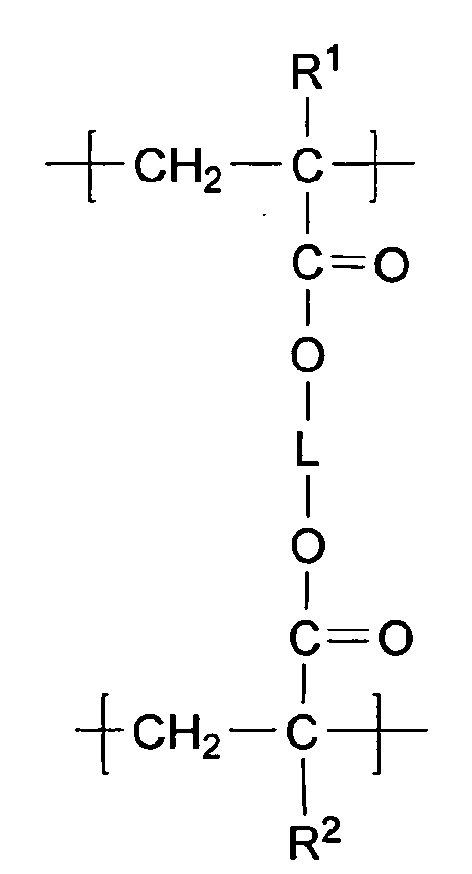
- the organic layer comprises a polymer having a structural unit of the following formula (1):
- R 1 and R 2 each independently represent a hydrogen atom or a methyl group.
- R 1 and R 2 are the same.
- L represents an open-chain alkylene group having at least 8 carbon atoms and not containing an oxygen atom, a nitrogen atom and a sulfur atom.
- Open-chain as referred to herein means a structure not containing a cyclic structure.
- L has from 8 to 12 carbon atoms, more preferably from 8 to 10 carbon atoms, even more preferably 8 or 9 carbon atoms.
- the alkylene group constituting L may be substituted or not substituted.
- an example of the substituent for the alkylene group is an alkyl group, for example, including a methyl group, an ethyl group, an n-propyl group, an n-butyl group, an n-pentyl group, an n-hexyl group.
- the number of the carbon atoms constituting the alkyl group is preferably from 1 to 6, more preferably from 2 to 4.
- the organic layer may contain plural types of the structures of formula (1), or may contain only one type of the structure.
- the polymer that constitutes the organic layer contain from 50 to 100% by mass of the structure of formula (1), more preferably from 60 to 100% by mass, even more preferably from 70 to 100% by mass, still more preferably from 70 to 95% by mass thereof.
- the structure except the structure of formula (1) may be any one not too much detracting from the object of the invention.
- the additional structure contains a structural unit derived from acrylate monomers or methacrylate monomers.
- the polymer constituting the organic layer is preferably produced through polymerization of a monomer mixture comprising, as the essential ingredient thereof, an acrylate or a methacrylate.
- the monomer mixture to be used herein includes a bifunctional monomer of the following formula (2): (2) Ac 1 -O-L-O-Ac 2
- Ac 1 and Ac 2 each represent an acryloyl group or a methacryloyl group;
- L represents an open-chain alkylene group having at least 8 carbon atoms and not containing an oxygen atom, a nitrogen atom and a sulfur atom.
- the details of L and the preferred range thereof are the same as those described hereinabove for L in formula (1).
- bifunctional monomer of formula (2) examples are described below, to which, however, the bifunctional monomer of formula (2) for use in the invention should not be limited.
- the bifunctional monomer of formula (2) is characterized by low surface energy and good wettability and spreadability in coating.
- the surface energy may be evaluated by measuring the contact angle to water or diiodomethane of the surface of the organic layer formed by curing the monomer.
- the bifunctional monomer of formula (2) for use in the invention is preferably such that the contact angle to water of the cured layer is at least 70 degrees, more preferably at least 75 degrees; and even more preferably, the contact angle to water of the layer is at least 75 degrees and the contact angle to diiodomethane of the layer is at least 40 degrees.
- the bifunctional monomer of formula (2) may be a single monomer or a mixture of plural types of monomers.
- the content of the bifunctional monomer of formula (2) to be in the monomer mixture for use in the invention is preferably from 50 to 100% by mass.
- the monomer mixture for use in the invention may contain any other bifunctional acrylate or methacrylate monomer than the bifunctional monomer of formula (2).
- the monomer mixture for use in the invention may contain a monofunctional acrylate or methacrylate monomer, a trifunctional acrylate or methacrylate monomer, a tetrafunctional or more polyfunctional acrylate or methacrylate monomer.
- Preferred examples of the acrylate and the methacrylate usable in the invention are, for example, the compounds described in USP 6. 083, 628 , 6, 214, 422 . Some of them are shown below.
- the organic layer may additionally contain a polymer not having the structural unit of formula (1).
- additional polymer are polyester, methacrylic acid/maleic acid copolymer, polystyrene, transparent fluororesin, polyimide, fluoropolyimide, polyamide, polyamidimide, polyether imide, cellulose acylate, polyurethane, polyether ether ketone, polycarbonate, alicyclic polyolefin, polyarylate, polyether sulfone, polysulfone, fluorene ring-modified polycarbonate, alicyclic-modified polycarbonate, fluorene ring-modified polyester.
- the content of the polymer not having the structural unit of formula (1) in the organic layer is preferably from 5 to 50% by mass, more preferably from 10 to 40% by mass, even more preferably from 20 to 35% by mass.
- the solution coating method includes, for example, a dip coating method, an air knife coating method, a curtain coating method, a roller coating method, a wire bar coating method, a gravure coating method, a slide coating method, and an extrusion coating method of using a hopper as in USP 2, 681, 294 .
- the vacuum film formation method is preferably a flash vacuum evaporation method as in USP 4, 842, 893 , 4,954,371 , 5,032,461 .
- the monomer polymerization method is not specifically defined, for which, for example, preferred is thermal polymerization, light (UV, visible ray) polymerization, electronic beam polymerization, plasma polymerization or their combination. Of those, especially preferred is photopolymerization. In photopolymerization, a photopolymerization initiator may be used.
- the photopolymerization initiator examples include Irgacure series (e.g., Irgacure 651, Irgacure 754, Irgacure 184, Irgacure 2959, Irgacure 907, Irgacure 369, Irgacure 379, Irgacure 819) sold by Ciba Specialty Chemicals; Darocure series (e.g., Darocure TPO, Darocure 1173); Quantacure PDO; Esacure series (e.g., Esacure TZM, Esacure TZT) sold by Sartomer.
- the monomer is polymerized after the monomer mixture has been layerwise disposed.
- the light for irradiation is generally UV light from high-pressure mercy lamp or low-pressure mercy lamp.
- the irradiation energy is preferably at least 0.5 J/cm 2 , more preferably at least 2 J/cm 2 . Since acrylate and methacrylate receive polymerization inhibition by oxygen in air, it is desirable that the oxygen concentration or the oxygen partial pressure during the monomer polymerization is reduced. In case where the oxygen concentration in polymerization is lowered by a nitrogen substitution method, the oxygen concentration is preferably at most 2%, more preferably at most 0.5%. In case where the oxygen partial pressure in polymerization is lowered by a pressure reduction method, the total pressure is preferably at most 1000 Pa, more preferably at most 100 Pa. Especially preferred is UV polymerization with energy irradiation of at least 2 J/cm 2 under a reduced pressure condition of at most 100 Pa.
- the thickness of the organic layer is not specifically defined. However, when too thin, the layer could not be uniform; but when too thick, the layer may be cracked and its barrier capability may lower. From these viewpoints, the thickness of the organic layer is preferably from 10 nm to 2000 nm, more preferably from 20 nm to 1000 nm.
- the hardness of the organic layer is high. It is known that, when the hardness of the organic layer is high, then the inorganic layer may be formed smoothly, and as a result, the barrier capability of the laminate may increase.
- the hardness of the organic layer may be represented by a microhardness scale based on a nanoindentation method.
- the microhardness of the organic layer is preferably at least 150 N/mm, more preferably at least 180 N/mm, even more preferably at least 200 N/mm.
- the lamination of the organic layer and the inorganic layer may be attained by successively and repeatedly forming the organic layer and the inorganic layer in accordance with the intended layer constitution.
- the inorganic layer is formed according to a vacuum film formation method such as a sputtering method, a vacuum evaporation method, an ion plating method or a plasma CVD method
- the organic layer is formed also according to a vacuum film formation method such as the above-mentioned flash vapor deposition method.
- the barrier layer is formed, it is especially desirable that the organic layer and the inorganic layer are laminated all the time in a vacuum of at most 1000 Pa, not restoring the pressure to an atmospheric pressure during the film formation. More preferably, the pressure is at most 100 Pa, even more preferably at most 50 Pa, still more preferably at most 20 Pa.
- the barrier laminate of the invention is formed on a support. Selecting the support, the barrier laminate may have various applications.
- the support includes a substrate film, as well as various devices, optical members, etc.
- the barrier laminate of the invention may be used as a barrier layer of a barrier film substrate.
- the barrier laminate and the barrier film substrate of the invention may be used for sealing up devices that require gas-barrier performance.
- the barrier laminate and the barrier film substrate of the invention may apply optical members. These are described in detail hereinunder.
- the barrier film substrate comprises a substrate film and a barrier laminate formed on the substrate film.
- the barrier laminate of the invention may be provided only one surface of the substrate film, or may be provided on both surfaces thereof.
- the barrier laminate of the invention may be laminated in an order of an inorganic layer and an organic layer from the side of the substrate film; or may be laminated in an order of an organic layer and an inorganic layer from it.
- the uppermost layer of the laminate of the invention may be an inorganic layer or an organic layer.
- the barrier film substrate of the invention is a film substrate having a barrier layer that functions to block oxygen, water, nitrogen oxide, sulfur oxide, ozone and others in air.
- the number of the layers that constitutes the barrier film substrate may be typically from 2 layers to 30 layers, more preferably from 3 layers to 20 layers.
- the barrier film substrate may have any other constitutive components (e.g., functional layers such as adhesive layer) in addition to the barrier laminate and the substrate film.
- the functional layer may be disposed on the barrier laminate, or between the barrier laminate and the substrate film, or on the side (back) of the substrate film not coated with the barrier laminate.
- the substrate film is generally a plastic film.
- the plastic film usable herein may be any one capable of supporting a laminate of an organic layer and an inorganic layer; and it may be suitably selected depending on the use and the object thereof.
- the plastic film includes metal supports (e.g., aluminium, copper, stainless), and thermoplastic resins such as polyester resin, methacryl resin, methacrylic acid-maleic anhydride, polystyrene resin, transparent fluororesin, polyimide, fluoropolyimide resin, polyamide resin, polyamidimide resin, polyetherimide resin, cellulose acylate resin, polyurethane resin, polyether ether ketone resin, polycarbonate resin, alicyclic polyolefin resin, polyarylate resin, polyether sulfone resin, polysulfone resin, cycloolefin copolymer, fluorene ring-modified polycarbonate resin, alicyclic-modified polycarbonate resin, fluorene ring-modified polyester resin, acryloyl compound.
- thermoplastic resins such as polyester resin, methacryl resin, methacrylic acid-maleic anhydride, polystyrene resin, transparent fluororesin, polyimide, fluor
- the plastic film is formed of a heat-resistant material.
- the plastic film is preferably formed of a heat-resistant transparent material having a glass transition temperature (Tg) of not lower than 100°C and/or a linear thermal expansion coefficient of at least 40 ppm/°C. Tg and the linear expansion coefficient may be controlled by the additives to the material.
- the thermoplastic resin of the type includes, for example, polyethylene naphthalate (PEN: 120°C), polycarbonate (PC: 140°C), alicyclic polyolefin (e. g.
- the plastic film is transparent, or that is, its light transmittance is generally at least 80%, preferably at least 85%, more preferably at least 90%.
- the light transmittance may be measured according to the method described in JIS-K7105. Concretely, using an integrating sphere-type light transmittance meter, a whole light transmittance and a quantity of scattered light are measured, and the diffusive transmittance is subtracted from the whole transmittance to obtain the intended light transmittance of the sample.
- a nontransparent material may be used for the plastic film.
- the nontransparent material includes, for example, polyimide, polyacrylonitrile, known liquid-crystal polymer.
- the thickness of the plastic film for use in the barrier film substrate of the invention may be suitably selected depending on its use. Typically, the thickness may be from 1 to 800 ⁇ m, preferably from 10 to 200 ⁇ m.
- the plastic film may have a functional layer such as a transparent conductive layer, a primer layer, etc. The functional layer is described in detail in JP-A 2006-289627 , paragraphs 0036 to 0038.
- Examples of other functional layers than those are a matting agent layer, a protective layer, an antistatic layer, a planarizing layer, an adhesiveness improving layer, a light shielding layer, an antireflection layer, a hard coat layer, a stress relaxing layer, an antifogging layer, an anti-soiling layer, a printable layer, an adhesive layer, etc.
- the barrier laminate and the barrier film substrate of the invention are favorably used for devices that are deteriorated by the chemical components in air (e.g., oxygen, water, nitrogen oxide, sulfur oxide, ozone).
- the devices are, for example, organic EL devices, liquid-crystal display devices, thin-film transistors, touch panels, electronic papers, solar cells, other electronic devices. More preferred are organic EL devices.
- the barrier laminate of the invention may be used for film-sealing of devices. Specifically, this is a method of providing a barrier laminate of the invention on the surface of a device serving as a support by itself. Before providing the barrier laminate, the device may be covered with a protective layer.
- the barrier film substrate of the invention may be used as a substrate of a device or as a film for sealing up according to a solid sealing method.
- the solid sealing method comprises forming a protective layer on a device, then forming an adhesive layer and a barrier film substrate as laminated thereon, and curing it.
- the adhesive may be a thermosetting epoxy resin, a photocurable acrylate resin, etc.
- Examples of an organic EL device with a barrier film substrate are described in detail in JP-A 2007-30387 .
- a reflection-type liquid-crystal display device has a constitution of an under substrate, a reflection electrode, a lower alignment film, a liquid-crystal layer, an upper alignment layer, a transparent electrode, an upper substrate, a ⁇ /4 plate and a polarizing film, formed in that order from the bottom.
- the barrier film substrate of the invention may be used as the transparent electrode substrate and the upper substrate.
- a color filter layer is additionally provided between the reflection electrode and the lower alignment film, or between the upper alignment film and the transparent electrode.
- a transmission-type liquid-crystal display device has a constitution of a backlight, a polarizer, a ⁇ /4 plate, a lower transparent electrode, a lower alignment film, a liquid-crystal layer, an upper alignment film, an upper transparent electrode, an upper substrate, a ⁇ /4 plate and a polarizing film, formed in that order from the bottom.
- the substrate of the invention may be sued as the upper transparent electrode and the upper substrate.
- a color filter layer is additionally provided between the lower transparent electrode and the lower alignment film, or between the upper alignment film and the transparent electrode.
- the type of the liquid-crystal cell is a TN (twisted nematic) type, an STN (super-twisted nematic) type, a HAN (hybrid aligned nematic) type, a VA (Vertically Alignment) type, an ECB (Electrically Controlled Birefringence) type, an OCB (optically compensatory bent) type, or a CPA (continuous pinwheel alignment) type.
- TN twisted nematic
- STN super-twisted nematic
- HAN hybrid aligned nematic
- VA Very Alignment
- ECB Electrically Controlled Birefringence
- OCB optical compensatory bent
- CPA continuous pinwheel alignment
- optical member that comprises the barrier laminate of the invention is a circular polarizer.
- Laminating a barrier film substrate of the invention with a ⁇ /4 plate and a polarizer gives a circular polarizer.
- the components are so laminated that the slow axis of the ⁇ /4 plate could cross the absorption axis of the polarizer at an angle of 45°.
- the polarizer is preferably stretched in the direction of 45° from the machine direction (MD) thereof; and for example, those described in JP-A 2002-865554 are favorably used.
- Neotex Q65FA polyethylene naphthalate film
- a first inorganic layer (aluminium oxide) was formed on the smooth surface of the polyethylene naphthalate film. Aluminium was used as the target; argon was used as the discharge gas; and oxygen was used as the reaction gas. The film formation pressure was 0.1 Pa; and the ultimate film thickness was 50 nm.
- barrier film substrates of the invention samples 1 and 2
- comparative barrier film substrates samples 3 to 8
- the film thickness was 500 nm ⁇ 50 nm.
- the contact angle to water and diiodomethane (CH 2 I 2 ) of the surface of the first organic layer of samples 1 to 8 was measured, using a contact angle gauge (CA-X Model by Kyowa Kaimen Kagaku). The data are shown in Table 1.
- the barrier laminates were analyzed for the adhesiveness.
- the samples were expressed by the ratio (percentage) of the area of the film not broken; and the data are shown in Table 1. Larger data mean higher adhesiveness.
- the barrier film substrates of the invention, samples 1 and 2 had a large contact angle to water after organic layer film formation, of 79.5 degrees and 75.5 degrees; and they are hydrophobic and had low surface energy.
- the comparative barrier film substrates, samples 3 to 8 had a contact angle to water after organic layer formation, of less than 75 degrees; and as compared with that of the organic layer in the invention, the hydrophilicity of the organic layer in the comparative samples was higher and the surface energy thereof was larger.
- the barrier film substrates of the invention samples 1 and 2 had higher adhesiveness, as compared with the comparative barrier film substrates, samples 3 to 8.
- the contact angle to diiodomethane of the sample 1 was 29.9 degrees, while that of the sample 2 was 42.0 degrees and was large. This means that the surface energy dispersion force component of the organic layer of the sample 2 is smaller. As a result, the adhesiveness of the sample 2 is higher having a significant difference, and the sample 2 is much superior to the others.
- Neotex Q65FA polyethylene naphthalate film
- a first inorganic layer (aluminium oxide) was formed on the smooth surface of the polyethylene naphthalate film. Aluminium was used as the target; argon was used as the discharge gas; and oxygen was used as the reaction gas. The film formation pressure was 0.1 Pa; and the ultimate film thickness was 50 nm.
- barrier film substrates of the invention samples 11 to 13
- comparative barrier film substrates samples 14 and 15
- the film thickness was 500 nm ⁇ 50 nm.
- the barrier film substrates of the invention samples 11 to 13 had higher adhesiveness, as compared with the comparative barrier film substrates, samples 14 and 15.
- samples 11 to 13 was higher. This confirms that the vacuum polymerization at an inner pressure of at most 100 Pa gives better barrier film substrates having much higher adhesiveness, as compared with the polymerization in an atmosphere in which the oxygen concentration is reduced to at most 0.5% by nitrogen substitution.
- Table 2 Sample No.
- a polyethylene naphthalate film (Teijin DuPont's trade name, Neotex Q65FA) was cut into 20 cm x 20 cm pieces.
- an organic/inorganic laminate film formation device (Vitex Systems' Guardian 200)
- Guardian 200 is a device for producing an organic/inorganic lamination-type barrier laminate. In this, an organic layer and an inorganic layer are continuously formed all in vacuum, and therefore, the barrier laminate to be produced therein is not exposed to open air until the completion of its production.
- the inorganic layer formation method in the device is flash vapor evaporation at an inner pressure of 3 Pa, and the UV radiation energy for polymerization was 2 J/cm 2 .
- the material for the organic layer used was a mixture solution of 1,9-nonanediol acrylate (Kyoeisha Chemical's trade name, Light-Acrylate, 80 g), Kyoeisha's Light-Acrylate TMP-A (10 g), Kyoeisha's Light-Acrylate BO-A (5 g), and a UV polymerization initiator (EZACURE-TZT, 5 g).
- inorganic film formation employed was aluminium oxide film formation according to a DC-pulse reactive sputtering method with aluminium as a target (in which the reaction gas is oxygen).
- the thickness of the formed organic layer was 500 nm/layer; the thickness of the formed inorganic layer (aluminium oxide) was 50 nm/layer.
- barrier film substrates, samples 21 to 23 were constructed.
- sample 24 was constructed, having a layer constitution of "inorganic layer/organic layer/substrate/organic layer/inorganic layer".
- a comparative barrier film substrate, sample 25 was constructed, having a layer constitution of "inorganic layer/organic layer/inorganic layer/substrate".
- a comparative barrier film substrate, sample 26 was constructed, having a layer constitution of "inorganic layer/organic layer/inorganic layer/substrate".
- sample 27 In the same manner as that for the sample 25 but forming an organic layer and an inorganic layer in order on both surfaces of the above substrate (polyethylene terephthalate film), a barrier film substrate, sample 27 was constructed, having a layer constitution of "inorganic layer/organic layer/substrate/organic layer/inorganic layer".
- the water vapor permeability of all the barrier film substrates of the invention, samples 21 to 24 was lower than the detection limit of the tester, 0.01 g/m 2 ⁇ day; however, the water vapor permeability of the comparative barrier film substrates, samples 25 to 27, for which was used a cyclic structure-having acrylate, was 0.08 g/m 2 ⁇ day, 0.06 g/m 2 ⁇ day and 0.02 g/m 2 ⁇ day, respectively.
- lithium fluoride was vapor-deposited in a thickness of 1 nm and metal aluminium was in a thickness of 100 nm in that order, serving as a cathode.
- a silicon nitride film having a thickness of 5 ⁇ m was formed according to a parallel plate CVD method, thereby constructing an organic EL device (OEL-1, 2).
- thermosetting adhesive (Daizo-Nichimori's Epotec 310)
- the device was stuck to the barrier film substrate, sample 21 to 23 (sealing film), and heated at 65°C for 3 hours to cure the adhesive.
- organic EL devices (BOEL-1 to 3) were obtained.
- Table 4 Organic EL Device Sealing film
- the organic EL devices (BOEL-1 to 3) were driven for light emission with a voltage of 7V applied thereto from a current/voltage generator (Keithley's SMU2400 Model source measure unit). Using a microscope, the surface of each sample was checked for its condition with light emission, and it was confirmed that all the devices gave uniform light emission with no dark spot.
- the devices were kept in a dark room at 40°C and a relative humidity of 90% for 60 days, and checked for the surface condition with light emission.
- the ratio of the emission area after storage to the emission area before storage was 92% in BOEL-1, 93% in BOEL-2, and 96% in BOEL-3, and all the devices gave no dark spot.
- the organic EL device constructed in "(1) Construction of Organic EL Device” was sealed up with the organic/inorganic laminate barrier film (the barrier laminate of the invention), using the organic/inorganic laminate film formation device according to the method described in "(3-1) Construction of Barrier Film Substrate in organic/inorganic vacuum integrated lamination system”.
- the thus-sealed organic EL devices were evaluated for the surface condition with light emission, according to the evaluation method described in " (3) Evaluation of Organic EL device for the surface condition with light emission", and they gave no dark spot like the above sealed with a barrier film substrate.
- the organic layer and the inorganic layer are hardly delaminated, and the laminate and the substrate have a low water vapor permeability.
- the barrier laminate and the barrier film substrate may be readily produced.
- the barrier laminate and the barrier film substrate of the invention can be used as sealing films, and in particular, the barrier film laminate of the invention is useful as a substitute for conventional glass substrates. Accordingly, the invention is widely applicable to various industrial products, typically for example, to various devices such as organic EL devices.
Landscapes
- Chemical & Material Sciences (AREA)
- Health & Medical Sciences (AREA)
- Chemical Kinetics & Catalysis (AREA)
- Medicinal Chemistry (AREA)
- Polymers & Plastics (AREA)
- Organic Chemistry (AREA)
- Toxicology (AREA)
- General Chemical & Material Sciences (AREA)
- Inorganic Chemistry (AREA)
- Laminated Bodies (AREA)
- Electroluminescent Light Sources (AREA)
Abstract
Description
- The present invention relates to a barrier laminate, especially to a barrier laminate having excellent adhesiveness and having a low water vapor permeability, and also relates to a barrier film substrate comprising the barrier laminate and to a device such as an organic EL device (organic electroluminescent device) comprising it.
- Heretofore, a barrier film fabricated by forming a thin metal oxide film of aluminium oxide, magnesium oxide or silicon oxide on the surface of a plastic film is widely used for wrapping or packaging articles that require shielding from various gases such as water vapor or oxygen and for wrapping or packaging edibles, industrial articles and medicines for preventing them from being deteriorated.
- Recently, in the field of liquid-crystal display devices and organic EL devices, plastic film substrates are being used in place of glass substrates that are heavy and readily cracked or broken. As applicable to a roll-to-roll system, plastic film substrates are advantageous in point of cost. However, plastic film substrates are problematic in that their gas-barrier property is not good as compared with that of glass substrates. Therefore, when a plastic film substrate is used in a liquid-crystal display device, then water vapor may penetrate into the liquid-crystal cell, thereby causing display failures.
- For solving the problem, it is known to form a water vapor barrier layer on a plastic film, thereby using the resulting barrier film substrate. As such a barrier film substrate, there are known a plastic film coated with silicon oxide through vapor deposition (for example, see
JP-B 53-12953 JP-A 58-217344 - However, substrates for use in organic EL devices require a further higher water vapor barrier level. To satisfy the requirement, there have been reported a technique of forming a laminate of an organic layer and an inorganic layer as a barrier layer, thereby realizing a water vapor permeability of less than 0.1 g/m2·day (for example, see
JP-A 2003-335880 JP-A 2003-335820 USP 6, 413, 645 ). - However, the organic/inorganic laminate-type barrier film substrates disclosed in these still have some problems in that their barrier capability is not always satisfactory for use in organic EL devices and that the organic layer and the inorganic layer may be readily delaminated owing to mechanical stress applied thereto. Accordingly, it is desired to develop an organic/inorganic laminate-type barrier laminate having good adhesiveness, and a gas-barrier film substrate with the laminate formed on a plastic film, and also a device such as an organic EL device comprising it.
- A first object of the invention is to provide an organic/inorganic laminate-type barrier laminate having a water vapor permeability of less than 0.01 g/m2·day and having good adhesiveness, and to provide a barrier film substrate comprising it. A second object of the invention is to provide a device of high durability, comprising the barrier laminate or the barrier film substrate.
- The present inventors have assiduously studied and, as a result, have found that, in a barrier laminate comprising an organic layer and an inorganic layer, when an acrylate or methacrylate having a relatively high degree of hydrophobicity is essentially used as the monomer for producing the polymer for use in forming the organic layer, then the mechanical strength (adhesiveness) of the barrier laminate fabricated may be increased, and have completed the present invention described below.
- [1] A barrier laminate comprising at least one organic layer and at least one inorganic layer, in which the organic layer comprises a polymer having a structural unit of the following formula (1):

- [2] The barrier laminate of [1], wherein the polymer has the structural unit of formula (1) in an amount of from 50% by mass to 100% by mass.
- [3] The barrier laminate of [1] or [2], wherein the contact angle to water of the organic layer is at least 75 degrees, and the contact angle to diiodomethane of the organic layer is at least 40 degrees.
- [4] A barrier film substrate having the barrier laminate of any one of [1] to [3], on at least one surface of a plastic film.
- [5] The barrier film substrate of [4], which has the barrier laminate on both surfaces of the plastic film.
- [6] The barrier film substrate of [4] or [5], which has, on one surface of the plastic film, at least one layer of the barrier laminate and a matting agent layer provided thereon, and has, on the other surface thereof, at least one layer of the barrier laminate.
- [7] A method for producing a barrier laminate having at least one organic layer and at least one inorganic layer, which comprises polymerizing a monomer mixture that contains a bifunctional monomer of the following formula (2), thereby forming the organic layer:
Formula (2) Ac1-O-L-O-Ac2
wherein Ac1 and Ac2 each independently represent an acryloyl group or a methacryloyl group; L represents an open-chain alkylene group having at least 8 carbon atoms and not containing an oxygen atom, a nitrogen atom and a sulfur atom. - [8] The method for producing a barrier laminate of [7], wherein the content of the bifunctional monomer of formula (2) in the monomer mixture is from 50% by mass to 100% by mass.
- [9] The method for producing a barrier laminate of [7] or [8], which comprises laminating the organic layer and the inorganic layer all the time in a vacuum of at most 100 Pa, thereby forming the barrier laminate.
- [10] The method for producing a barrier laminate of any one of [7] to [9], which comprises polymerizing the monomer mixture in a vacuum of at most 100 Pa.
- [11] The method for producing a barrier laminate of [10], which comprises polymerizing the monomer mixture by UV with energy irradiation of at least 2 J/cm2 in a vacuum of at most 100 Pa.
- [12] A method for producing a barrier film substrate, which comprises forming a barrier laminate on at least one surface of a plastic film according to the production method of any one of [7] to [11].
- [13] The method for producing a barrier film substrate of [12], which comprises forming, on one surface of the plastic film, at least one layer of the barrier laminate and further forming a matting agent layer on it, and forming, on the other surface thereof, at least one layer of the barrier laminate, in no special order.
- [14] A device sealed up with the barrier laminate of any one of [1] to [3].
- [15] A device comprising, as the substrate thereof, a barrier film substrate of any one of [4] to [6].
- [16] A device sealed up with a barrier film substrate of any one of [4] to [6].
- [17] The device of any one of [14] to [16], which is an electronic device.
- [18] The device of any one of [14] to [16], which is an organic EL device.
- [19] An optical member comprising, as the substrate thereof, the barrier film substrate of any one of [4] to [6].
- In the barrier laminate and the barrier film substrate of the invention, the organic layer and the inorganic layer are hardly delaminated owing to the mechanical stress between them; and the laminate and the substrate therefore have a low water vapor permeability. According to the production method of the invention, the barrier laminate and the barrier film substrate can be produced with ease. The device of the invention has high durability.
- The barrier laminate and its production method, the barrier film substrate and its production method, and the device of the invention are described in detail hereinunder. The description made hereinunder is for some typical embodiments of the invention, to which, however, the invention should not be limited. In this description, the numerical range expressed by the wording "a number to another number" means the range that falls between the former number indicating the lowermost limit of the range and the latter number indicating the uppermost limit thereof. In the structural formulae in this description, O indicates an oxygen atom.
- The barrier laminate of the invention comprises at least one organic layer and at least one inorganic layer. It is characterized in that the organic layer comprises a polymer having the structural unit of formula (1).
- The barrier laminate of the invention may be formed on any substrate regardless of the type thereof. For example, the barrier laminate may be directly formed on a device such as an organic semiconductor device that requires gas-barrier capability, or may be formed separately on a substrate to construct a barrier film substrate.
- The inorganic layer and the organic layer, which are the indispensable structural elements of the barrier laminate of the invention, are described in detail hereinunder. The substrate on which the barrier laminate may be formed is described in the section of the barrier film substrate to be given hereinunder.
- The inorganic layer is, in general, a layer of a thin film formed of a metal compound. For forming the inorganic layer, employable is any method capable of producing the intended thin film. For it, for example, suitable is a coating method, sputtering method, a vacuum evaporation method, an ion-plating method or a plasma CVD method. Concretely, the methods described in Japanese Patent No.
3400324 JP-A 2002-322561 2002-361774 - Not specifically defined, the component to be in the inorganic layer may be any one that satisfies the above-mentioned performance, for which, for example, employable are oxides, nitrides or oxinitrides containing at least one metal selected from Si, Al, In, Sn, Zn, Ti, Cu, Ce and Ta. Of those preferred are oxides, nitrides or oxinitrides of a metal selected from Si, Al, In, Sn, Zn and Ti; and more preferred are metal oxides, nitrides or oxinitrides with Si or Al. These may contain any other element as a subsidiary component.
- Not specifically defined, the thickness of the inorganic layer is preferably within a range of from 5 nm to 500 nm, more preferably from 10 nm to 200 nm. Two or more inorganic layers may be laminated, and in such a case, the constitutive layers may have the same or different compositions.
- The organic layer comprises a polymer having a structural unit of the following formula (1):

- In formula (1), R1 and R2 each independently represent a hydrogen atom or a methyl group. Preferably, R1 and R2 are the same.
- L represents an open-chain alkylene group having at least 8 carbon atoms and not containing an oxygen atom, a nitrogen atom and a sulfur atom. "Open-chain" as referred to herein means a structure not containing a cyclic structure. Preferably, L has from 8 to 12 carbon atoms, more preferably from 8 to 10 carbon atoms, even more preferably 8 or 9 carbon atoms. The alkylene group constituting L may be substituted or not substituted. An example of the substituent for the alkylene group is an alkyl group, for example, including a methyl group, an ethyl group, an n-propyl group, an n-butyl group, an n-pentyl group, an n-hexyl group. The number of the carbon atoms constituting the alkyl group is preferably from 1 to 6, more preferably from 2 to 4.
- The organic layer may contain plural types of the structures of formula (1), or may contain only one type of the structure. Preferably, the polymer that constitutes the organic layer contain from 50 to 100% by mass of the structure of formula (1), more preferably from 60 to 100% by mass, even more preferably from 70 to 100% by mass, still more preferably from 70 to 95% by mass thereof. Not specifically defined, the structure except the structure of formula (1) may be any one not too much detracting from the object of the invention. Preferably, the additional structure contains a structural unit derived from acrylate monomers or methacrylate monomers.
- The polymer constituting the organic layer is preferably produced through polymerization of a monomer mixture comprising, as the essential ingredient thereof, an acrylate or a methacrylate. The monomer mixture to be used herein includes a bifunctional monomer of the following formula (2):
(2) Ac1-O-L-O-Ac2
- In formula (2), Ac1 and Ac2 each represent an acryloyl group or a methacryloyl group; L represents an open-chain alkylene group having at least 8 carbon atoms and not containing an oxygen atom, a nitrogen atom and a sulfur atom. The details of L and the preferred range thereof are the same as those described hereinabove for L in formula (1).
- Examples of the bifunctional monomer of formula (2) are described below, to which, however, the bifunctional monomer of formula (2) for use in the invention should not be limited.

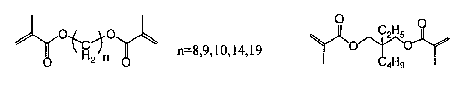

- The bifunctional monomer of formula (2) is characterized by low surface energy and good wettability and spreadability in coating. In general, the surface energy may be evaluated by measuring the contact angle to water or diiodomethane of the surface of the organic layer formed by curing the monomer. The bifunctional monomer of formula (2) for use in the invention is preferably such that the contact angle to water of the cured layer is at least 70 degrees, more preferably at least 75 degrees; and even more preferably, the contact angle to water of the layer is at least 75 degrees and the contact angle to diiodomethane of the layer is at least 40 degrees.
- The bifunctional monomer of formula (2) may be a single monomer or a mixture of plural types of monomers. The content of the bifunctional monomer of formula (2) to be in the monomer mixture for use in the invention is preferably from 50 to 100% by mass. The monomer mixture for use in the invention may contain any other bifunctional acrylate or methacrylate monomer than the bifunctional monomer of formula (2). In addition, the monomer mixture for use in the invention may contain a monofunctional acrylate or methacrylate monomer, a trifunctional acrylate or methacrylate monomer, a tetrafunctional or more polyfunctional acrylate or methacrylate monomer.
- Preferred examples of the acrylate and the methacrylate usable in the invention are, for example, the compounds described in
USP 6. 083, 628 ,6, 214, 422 . Some of them are shown below.
- Other examples in addition to the above are the following compounds that are available on the market in Japan.


- The organic layer may additionally contain a polymer not having the structural unit of formula (1). Examples of the additional polymer are polyester, methacrylic acid/maleic acid copolymer, polystyrene, transparent fluororesin, polyimide, fluoropolyimide, polyamide, polyamidimide, polyether imide, cellulose acylate, polyurethane, polyether ether ketone, polycarbonate, alicyclic polyolefin, polyarylate, polyether sulfone, polysulfone, fluorene ring-modified polycarbonate, alicyclic-modified polycarbonate, fluorene ring-modified polyester. The content of the polymer not having the structural unit of formula (1) in the organic layer is preferably from 5 to 50% by mass, more preferably from 10 to 40% by mass, even more preferably from 20 to 35% by mass.
- For forming the organic layer, herein employable is an ordinary solution coating method or a vacuum film formation method. The solution coating method includes, for example, a dip coating method, an air knife coating method, a curtain coating method, a roller coating method, a wire bar coating method, a gravure coating method, a slide coating method, and an extrusion coating method of using a hopper as in
USP 2, 681, 294 . Not specifically defined, the vacuum film formation method is preferably a flash vacuum evaporation method as inUSP 4, 842, 893 ,4,954,371 ,5,032,461 . - The monomer polymerization method is not specifically defined, for which, for example, preferred is thermal polymerization, light (UV, visible ray) polymerization, electronic beam polymerization, plasma polymerization or their combination. Of those, especially preferred is photopolymerization. In photopolymerization, a photopolymerization initiator may be used. Examples of the photopolymerization initiator are Irgacure series (e.g., Irgacure 651, Irgacure 754, Irgacure 184, Irgacure 2959, Irgacure 907, Irgacure 369, Irgacure 379, Irgacure 819) sold by Ciba Specialty Chemicals; Darocure series (e.g., Darocure TPO, Darocure 1173); Quantacure PDO; Esacure series (e.g., Esacure TZM, Esacure TZT) sold by Sartomer. Preferably, the monomer is polymerized after the monomer mixture has been layerwise disposed. For example, it is desirable that the monomer mixture is disposed on a substrate and then polymerized.
- The light for irradiation is generally UV light from high-pressure mercy lamp or low-pressure mercy lamp. The irradiation energy is preferably at least 0.5 J/cm2, more preferably at least 2 J/cm2. Since acrylate and methacrylate receive polymerization inhibition by oxygen in air, it is desirable that the oxygen concentration or the oxygen partial pressure during the monomer polymerization is reduced. In case where the oxygen concentration in polymerization is lowered by a nitrogen substitution method, the oxygen concentration is preferably at most 2%, more preferably at most 0.5%. In case where the oxygen partial pressure in polymerization is lowered by a pressure reduction method, the total pressure is preferably at most 1000 Pa, more preferably at most 100 Pa. Especially preferred is UV polymerization with energy irradiation of at least 2 J/cm2 under a reduced pressure condition of at most 100 Pa.
- The thickness of the organic layer is not specifically defined. However, when too thin, the layer could not be uniform; but when too thick, the layer may be cracked and its barrier capability may lower. From these viewpoints, the thickness of the organic layer is preferably from 10 nm to 2000 nm, more preferably from 20 nm to 1000 nm.
- Preferably, the hardness of the organic layer is high. It is known that, when the hardness of the organic layer is high, then the inorganic layer may be formed smoothly, and as a result, the barrier capability of the laminate may increase. The hardness of the organic layer may be represented by a microhardness scale based on a nanoindentation method. The microhardness of the organic layer is preferably at least 150 N/mm, more preferably at least 180 N/mm, even more preferably at least 200 N/mm.
- The lamination of the organic layer and the inorganic layer may be attained by successively and repeatedly forming the organic layer and the inorganic layer in accordance with the intended layer constitution. In case where the inorganic layer is formed according to a vacuum film formation method such as a sputtering method, a vacuum evaporation method, an ion plating method or a plasma CVD method, then it is desirable that the organic layer is formed also according to a vacuum film formation method such as the above-mentioned flash vapor deposition method. While the barrier layer is formed, it is especially desirable that the organic layer and the inorganic layer are laminated all the time in a vacuum of at most 1000 Pa, not restoring the pressure to an atmospheric pressure during the film formation. More preferably, the pressure is at most 100 Pa, even more preferably at most 50 Pa, still more preferably at most 20 Pa.
- In general, the barrier laminate of the invention is formed on a support. Selecting the support, the barrier laminate may have various applications. The support includes a substrate film, as well as various devices, optical members, etc. Concretely, the barrier laminate of the invention may be used as a barrier layer of a barrier film substrate. The barrier laminate and the barrier film substrate of the invention may be used for sealing up devices that require gas-barrier performance. The barrier laminate and the barrier film substrate of the invention may apply optical members. These are described in detail hereinunder.
- The barrier film substrate comprises a substrate film and a barrier laminate formed on the substrate film. In the barrier film substrate, the barrier laminate of the invention may be provided only one surface of the substrate film, or may be provided on both surfaces thereof. The barrier laminate of the invention may be laminated in an order of an inorganic layer and an organic layer from the side of the substrate film; or may be laminated in an order of an organic layer and an inorganic layer from it. The uppermost layer of the laminate of the invention may be an inorganic layer or an organic layer.
- The barrier film substrate of the invention is a film substrate having a barrier layer that functions to block oxygen, water, nitrogen oxide, sulfur oxide, ozone and others in air.
- Not specifically defined, the number of the layers that constitutes the barrier film substrate may be typically from 2 layers to 30 layers, more preferably from 3 layers to 20 layers.
- The barrier film substrate may have any other constitutive components (e.g., functional layers such as adhesive layer) in addition to the barrier laminate and the substrate film. The functional layer may be disposed on the barrier laminate, or between the barrier laminate and the substrate film, or on the side (back) of the substrate film not coated with the barrier laminate.
- In the barrier film substrate of the invention, the substrate film is generally a plastic film. Not specifically defined in point of the material and the thickness thereof, the plastic film usable herein may be any one capable of supporting a laminate of an organic layer and an inorganic layer; and it may be suitably selected depending on the use and the object thereof. Concretely, the plastic film includes metal supports (e.g., aluminium, copper, stainless), and thermoplastic resins such as polyester resin, methacryl resin, methacrylic acid-maleic anhydride, polystyrene resin, transparent fluororesin, polyimide, fluoropolyimide resin, polyamide resin, polyamidimide resin, polyetherimide resin, cellulose acylate resin, polyurethane resin, polyether ether ketone resin, polycarbonate resin, alicyclic polyolefin resin, polyarylate resin, polyether sulfone resin, polysulfone resin, cycloolefin copolymer, fluorene ring-modified polycarbonate resin, alicyclic-modified polycarbonate resin, fluorene ring-modified polyester resin, acryloyl compound.
- In case where the barrier film substrate of the invention is used as a substrate of a device such as an organic EL device to be mentioned hereinunder, it is desirable that the plastic film is formed of a heat-resistant material. Concretely, the plastic film is preferably formed of a heat-resistant transparent material having a glass transition temperature (Tg) of not lower than 100°C and/or a linear thermal expansion coefficient of at least 40 ppm/°C. Tg and the linear expansion coefficient may be controlled by the additives to the material. The thermoplastic resin of the type includes, for example, polyethylene naphthalate (PEN: 120°C), polycarbonate (PC: 140°C), alicyclic polyolefin (e. g. , Nippon Zeon's Zeonoa 1600: 160°C), polyarylate (PAr: 210°C), polyether sulfone (PES: 220°C), polysulfone (PSF: 190°C), cycloolefin copolymer (COC, compound described in
JP-A 2001-150584 JP-A 2000-227603 JP-A 2000-227603 JP-A 2002-80616 - Since the barrier film substrate of the invention is usable in devices such as organic EL devices, the plastic film is transparent, or that is, its light transmittance is generally at least 80%, preferably at least 85%, more preferably at least 90%. The light transmittance may be measured according to the method described in JIS-K7105. Concretely, using an integrating sphere-type light transmittance meter, a whole light transmittance and a quantity of scattered light are measured, and the diffusive transmittance is subtracted from the whole transmittance to obtain the intended light transmittance of the sample.
- Even when the barrier film substrate of the invention is used in displays, it does not always require transparency in a case where it is not disposed on the viewers' side. Accordingly in such a case, a nontransparent material may be used for the plastic film. The nontransparent material includes, for example, polyimide, polyacrylonitrile, known liquid-crystal polymer.
- Not specifically defined, the thickness of the plastic film for use in the barrier film substrate of the invention may be suitably selected depending on its use. Typically, the thickness may be from 1 to 800 µm, preferably from 10 to 200 µm. The plastic film may have a functional layer such as a transparent conductive layer, a primer layer, etc. The functional layer is described in detail in
JP-A 2006-289627 - The barrier laminate and the barrier film substrate of the invention are favorably used for devices that are deteriorated by the chemical components in air (e.g., oxygen, water, nitrogen oxide, sulfur oxide, ozone). Examples of the devices are, for example, organic EL devices, liquid-crystal display devices, thin-film transistors, touch panels, electronic papers, solar cells, other electronic devices. More preferred are organic EL devices.
- The barrier laminate of the invention may be used for film-sealing of devices. Specifically, this is a method of providing a barrier laminate of the invention on the surface of a device serving as a support by itself. Before providing the barrier laminate, the device may be covered with a protective layer.
- The barrier film substrate of the invention may be used as a substrate of a device or as a film for sealing up according to a solid sealing method. The solid sealing method comprises forming a protective layer on a device, then forming an adhesive layer and a barrier film substrate as laminated thereon, and curing it. Not specifically defined, the adhesive may be a thermosetting epoxy resin, a photocurable acrylate resin, etc.
- Examples of an organic EL device with a barrier film substrate are described in detail in
JP-A 2007-30387 - A reflection-type liquid-crystal display device has a constitution of an under substrate, a reflection electrode, a lower alignment film, a liquid-crystal layer, an upper alignment layer, a transparent electrode, an upper substrate, a λ/4 plate and a polarizing film, formed in that order from the bottom. In this, the barrier film substrate of the invention may be used as the transparent electrode substrate and the upper substrate. In color displays, it is desirable that a color filter layer is additionally provided between the reflection electrode and the lower alignment film, or between the upper alignment film and the transparent electrode. A transmission-type liquid-crystal display device has a constitution of a backlight, a polarizer, a λ/4 plate, a lower transparent electrode, a lower alignment film, a liquid-crystal layer, an upper alignment film, an upper transparent electrode, an upper substrate, a λ/4 plate and a polarizing film, formed in that order from the bottom. In this, the substrate of the invention may be sued as the upper transparent electrode and the upper substrate. In color displays, it is desirable that a color filter layer is additionally provided between the lower transparent electrode and the lower alignment film, or between the upper alignment film and the transparent electrode. Not specifically defined, the type of the liquid-crystal cell is a TN (twisted nematic) type, an STN (super-twisted nematic) type, a HAN (hybrid aligned nematic) type, a VA (Vertically Alignment) type, an ECB (Electrically Controlled Birefringence) type, an OCB (optically compensatory bent) type, or a CPA (continuous pinwheel alignment) type.
- Other applications of the invention are thin-film transistors as in
JP-T 10-512104 JP-A 5-127822 2002-48913 JP-A 2000-98326 7-160334 - An example of the optical member that comprises the barrier laminate of the invention is a circular polarizer.
- Laminating a barrier film substrate of the invention with a λ/4 plate and a polarizer gives a circular polarizer. In this case, the components are so laminated that the slow axis of the λ/4 plate could cross the absorption axis of the polarizer at an angle of 45°. The polarizer is preferably stretched in the direction of 45° from the machine direction (MD) thereof; and for example, those described in
JP-A 2002-865554 - The characteristics of the invention are described more concretely with reference to the following Examples. In the following Examples, the material used, its amount and the ratio, the details of the treatment and the treatment process may be suitably modified or changed. Accordingly, the invention should not be limitatively interpreted by the Examples mentioned below.
- A polyethylene naphthalate film (Teijin DuPont's trade name, Neotex Q65FA) was cut into 20 cm x 20 cm pieces, and a barrier laminate was formed on the side of the smooth surface thereof, and the thus-constructed samples were evaluated.
- Using a sputtering device, a first inorganic layer (aluminium oxide) was formed on the smooth surface of the polyethylene naphthalate film. Aluminium was used as the target; argon was used as the discharge gas; and oxygen was used as the reaction gas. The film formation pressure was 0.1 Pa; and the ultimate film thickness was 50 nm.
- On the first inorganic layer formed on the plastic film, a mixture solution of a monomer shown in Table 1 (20 g), a UV polymerization initiator (Ciba Speciality Chemicals' trade name, Ciba Irgacure 907) (0.6 g) and 2-butanone (190 g) was applied, using a wire bar, so as to form a liquid layer having a thickness of 5 µm. This was dried at room temperature for 2 hours, then put into a chamber having an oxygen concentration of 0.45% after nitrogen substitution, and the organic layer was cured therein through irradiation with UV light from a high-pressure mercury lamp (integrated radiation, about 2 J/cm2), thereby constructing barrier film substrates of the invention (samples 1 and 2) and comparative barrier film substrates (samples 3 to 8). In these, the film thickness was 500 nm ± 50 nm.
- The contact angle to water and diiodomethane (CH2I2) of the surface of the first organic layer of samples 1 to 8 was measured, using a contact angle gauge (CA-X Model by Kyowa Kaimen Kagaku). The data are shown in Table 1.
- According to a cross-cut peeling method based on JIS (Japan Industrial Standard) K5600-5-6 (ISO 2409), the barrier laminates were analyzed for the adhesiveness. For their evaluation, the samples were expressed by the ratio (percentage) of the area of the film not broken; and the data are shown in Table 1. Larger data mean higher adhesiveness.
- The barrier film substrates of the invention, samples 1 and 2 had a large contact angle to water after organic layer film formation, of 79.5 degrees and 75.5 degrees; and they are hydrophobic and had low surface energy. The comparative barrier film substrates, samples 3 to 8 had a contact angle to water after organic layer formation, of less than 75 degrees; and as compared with that of the organic layer in the invention, the hydrophilicity of the organic layer in the comparative samples was higher and the surface energy thereof was larger.
- The barrier film substrates of the invention, samples 1 and 2 had higher adhesiveness, as compared with the comparative barrier film substrates, samples 3 to 8.
- In comparison between sample 1 and sample 2, both the barrier film substrates of the invention, the contact angle to diiodomethane of the sample 1 was 29.9 degrees, while that of the sample 2 was 42.0 degrees and was large. This means that the surface energy dispersion force component of the organic layer of the sample 2 is smaller. As a result, the adhesiveness of the sample 2 is higher having a significant difference, and the sample 2 is much superior to the others.
Table 1 Sample No Monomer Contact Angle (degrees) Adhesiveness (%) Remarks Water CH2I2 Sample 1 1,9-nonanediol diacrylate 79.5 29.9 80 the invention Sample 2 2-butyl-2-ethyl-1,3-propanediol diacrylate 75.5 42.0 90 the invention Sample 3 1,6-hexanediol diacrylate 74.6 29.3 50 comparative sample Sample 4 neopentylglycol diacrylate 73.5 39.3 30 comparative sample Sample 5 bisphenol A ethylene oxide adduct diacrylate (number of EO added = 4) 74.0 32.4 40 comparative sample Sample 6 bisphenol A ethylene oxide adduct diacrylate (number of EO added = 10) 66.4 24.8 0 comparative sample Sample 7 bisphenol A propylene-oxide adduct diacrylate (number of EO added = 4) 74.6 36.2 0 comparative sample Sample 8 tripropylene glycol diacrylate 69.9 36.9 10 comparative sample - A polyethylene naphthalate film (Teijin DuPont's trade name, Neotex Q65FA) was cut into 20 cm x 20 cm pieces, and a barrier laminate was formed on the side of the smooth surface thereof, and the thus-constructed samples were evaluated.
- Using a sputtering device, a first inorganic layer (aluminium oxide) was formed on the smooth surface of the polyethylene naphthalate film. Aluminium was used as the target; argon was used as the discharge gas; and oxygen was used as the reaction gas. The film formation pressure was 0.1 Pa; and the ultimate film thickness was 50 nm.
- On the first inorganic layer formed on the plastic film, a mixture solution of a monomer shown in Table 2 (20 g), a UV polymerization initiator (Ciba Speciality Chemicals' trade name, Ciba Irgacure 907) (0.6 g) and 2-butanone (190 g) was applied, using a wire bar, so as to form a liquid layer having a thickness of 5 µm. This was dried at room temperature for 2 hours, then put into a vacuum chamber having an inner pressure of 30 Pa, and the organic layer was cured therein through irradiation with UV light from a high-pressure mercury lamp (integrated radiation, about 2 J/cm2), thereby constructing barrier film substrates of the invention (samples 11 to 13) and comparative barrier film substrates (samples 14 and 15). In these, the film thickness was 500 nm ± 50 nm.
- The adhesiveness was measured according to the same method as in the above (1-4). The data are shown in Table 2.
- The barrier film substrates of the invention, samples 11 to 13 had higher adhesiveness, as compared with the comparative barrier film substrates, samples 14 and 15.
- As compared with that of the above samples 1 and 2, the adhesiveness of the barrier film substrates of the invention, samples 11 to 13 was higher. This confirms that the vacuum polymerization at an inner pressure of at most 100 Pa gives better barrier film substrates having much higher adhesiveness, as compared with the polymerization in an atmosphere in which the oxygen concentration is reduced to at most 0.5% by nitrogen substitution.
Table 2 Sample No. Monomer Adhesiveness (%) Remarks Sample 11 1,9-nonanediol diacrylate 95 the invention Sample 12 2-butyl-2-ethyl-1,3-propanediol diacrylate 100 the invention Sample 13 1,9-nonanediol dimethacrylate 100 the invention Sample 14 tripropylene glycol diacrylate 15 comparative sample Sample 15 neopentyl glycol-modified trimethylolpropane diacrylate* 20 comparative sample * Nippon Kayaku's KAYARAD R-604 - A polyethylene naphthalate film (Teijin DuPont's trade name, Neotex Q65FA) was cut into 20 cm x 20 cm pieces. Using an organic/inorganic laminate film formation device (Vitex Systems' Guardian 200), a barrier laminate shown in Table 3 was formed on the side of the smooth surface of the film. Guardian 200 is a device for producing an organic/inorganic lamination-type barrier laminate. In this, an organic layer and an inorganic layer are continuously formed all in vacuum, and therefore, the barrier laminate to be produced therein is not exposed to open air until the completion of its production. The inorganic layer formation method in the device is flash vapor evaporation at an inner pressure of 3 Pa, and the UV radiation energy for polymerization was 2 J/cm2. As the material for the organic layer, used was a mixture solution of 1,9-nonanediol acrylate (Kyoeisha Chemical's trade name, Light-Acrylate, 80 g), Kyoeisha's Light-Acrylate TMP-A (10 g), Kyoeisha's Light-Acrylate BO-A (5 g), and a UV polymerization initiator (EZACURE-TZT, 5 g). For inorganic film formation, employed was aluminium oxide film formation according to a DC-pulse reactive sputtering method with aluminium as a target (in which the reaction gas is oxygen). The thickness of the formed organic layer was 500 nm/layer; the thickness of the formed inorganic layer (aluminium oxide) was 50 nm/layer. According to the production method of the invention as above, barrier film substrates, samples 21 to 23 were constructed.
- In the same manner as the above for the samples 21 to 23 but forming an organic layer and an inorganic layer in order on both surfaces of the substrate (polyethylene naphthalate film), a barrier film substrate, sample 24 was constructed, having a layer constitution of "inorganic layer/organic layer/substrate/organic layer/inorganic layer".
- In the same manner as the above for the samples 21 to 23 but using, as the material for the organic layer, a mixture used for the organic layer constituting the barrier film described in
JP-A 2003-335880 - In the same manner as the above for the samples 21 to 23 but using, as the material for the organic layer, a mixture used for the organic layer constituting the barrier film described in
JP-A 2003-335880 - In the same manner as that for the sample 25 but forming an organic layer and an inorganic layer in order on both surfaces of the above substrate (polyethylene terephthalate film), a barrier film substrate, sample 27 was constructed, having a layer constitution of "inorganic layer/organic layer/substrate/organic layer/inorganic layer".
- Using a water vapor permeability tester (MOCON's PERMATRAN-W3/31) , each sample was analyzed for the water vapor permeability at 40°C and a relative humidity of 90%. The detection limit of the tester is 0.01 g/m2·day. The data are shown in Table 3. The water vapor permeability of all the barrier film substrates of the invention, samples 21 to 24 was lower than the detection limit of the tester, 0.01 g/m2·day; however, the water vapor permeability of the comparative barrier film substrates, samples 25 to 27, for which was used a cyclic structure-having acrylate, was 0.08 g/m2·day, 0.06 g/m2·day and 0.02 g/m2·day, respectively.
- The above confirms that the barrier film substrates for which was used an open-chain acrylate satisfying the condition of the present invention are excellent in point of both the barrier capability and the adhesiveness.
Table 3 Sample No. Organic Layer Layer Constitution Water Vapor Permeability (g/m2/day) Remarks Sample 21 1,9-nonanediol diacrylate inorganic layer/ organic layer/ inorganic layer/ substrate lower than the detection limit the invention Sample 22 1,9-nonanediol diacrylate organic layer/ inorganic layer/ organic layer/ inorganic layer/ substrate lower than the than detection limit the invention Sample 23 1,9-nonanediol diacrylate inorganic layer/ organic layer/ inorganic layer/ organic layer/ substrat lower than the detection limit the invention Sample 24 1,9-nonanediol diacrylate inorganic layer/ substrate/ organic layer/ inorganic layer lower than the detection limit the invention Sample 25 dicyclopentadienyl diacrylate inorganic layer/ organic layer/ inorganic layer/ substrate 0.08 comparative sample Sample 26 neopentyl glycol-modified trimethylolpropane diacrylate inorganic layer/ organic layer/ inorganic layer/ substrate 0.06 comparative sample Sample 27 dicyclopentadienyl diacrylate inorganic layer/ organic layer/ substrate/ organic layer/ inorganic layer 0.04 comparative sample - An ITO film-coated conductive glass substrate (surface resistivity, 10 Ω/square) was washed with 2-propanol, and then subjected to UV-ozone treatment for 10 minutes. On this substrate (anode), the following organic compound layers were deposited in order according to a vapor deposition method.
(First Hole Transportation Layer) Copper Phthalocyanine thickness 10 nm (Second Hole Transportation Layer) N,N'-diphenyl-N,N'-dinaphthylbenzidine thickness 40 nm (Light Emission Layer serving also as electron transportation layer) Tris(8-hydroxyquinolinato)aluminium thickness 60 nm - Finally, lithium fluoride was vapor-deposited in a thickness of 1 nm and metal aluminium was in a thickness of 100 nm in that order, serving as a cathode. On this, a silicon nitride film having a thickness of 5 µm was formed according to a parallel plate CVD method, thereby constructing an organic EL device (OEL-1, 2).
- Using a thermosetting adhesive (Daizo-Nichimori's Epotec 310), the device was stuck to the barrier film substrate, sample 21 to 23 (sealing film), and heated at 65°C for 3 hours to cure the adhesive. Thus sealed, organic EL devices (BOEL-1 to 3) were obtained.
Table 4 Organic EL Device Sealing film BOEL-1 Sample 21 BOEL-2 Sample 22 BOEL-3 Sample 23 - Immediately after their construction, the organic EL devices (BOEL-1 to 3) were driven for light emission with a voltage of 7V applied thereto from a current/voltage generator (Keithley's SMU2400 Model source measure unit). Using a microscope, the surface of each sample was checked for its condition with light emission, and it was confirmed that all the devices gave uniform light emission with no dark spot.
- Next, the devices were kept in a dark room at 40°C and a relative humidity of 90% for 60 days, and checked for the surface condition with light emission. The ratio of the emission area after storage to the emission area before storage was 92% in BOEL-1, 93% in BOEL-2, and 96% in BOEL-3, and all the devices gave no dark spot.
- The organic EL device constructed in "(1) Construction of Organic EL Device" was sealed up with the organic/inorganic laminate barrier film (the barrier laminate of the invention), using the organic/inorganic laminate film formation device according to the method described in "(3-1) Construction of Barrier Film Substrate in organic/inorganic vacuum integrated lamination system". The thus-sealed organic EL devices were evaluated for the surface condition with light emission, according to the evaluation method described in " (3) Evaluation of Organic EL device for the surface condition with light emission", and they gave no dark spot like the above sealed with a barrier film substrate.
- The above confirms that the organic EL devices sealed with the barrier laminate of the invention have excellent wet heat durability.
- In the barrier laminate and the barrier film substrate of the invention, the organic layer and the inorganic layer are hardly delaminated, and the laminate and the substrate have a low water vapor permeability. According to the production method of the invention, the barrier laminate and the barrier film substrate may be readily produced. The barrier laminate and the barrier film substrate of the invention can be used as sealing films, and in particular, the barrier film laminate of the invention is useful as a substitute for conventional glass substrates. Accordingly, the invention is widely applicable to various industrial products, typically for example, to various devices such as organic EL devices.
Claims (20)
- A barrier laminate comprising at least one organic layer and at least one inorganic layer, in which the organic layer comprises a polymer having a structural unit of the following formula (1):

- The barrier laminate according to claim 1, wherein the polymer has the structural unit of formula (1) in an amount of from 50% by mass to 100% by mass.
- The barrier laminate according to claim 1 or 2, wherein the contact angle to water of the organic layer is at least 75 degrees, and the contact angle to diiodomethane of the organic layer is at least 40 degrees.
- A barrier film substrate having the barrier laminate of claim 1, on at least one surface of a plastic film.
- The barrier film substrate according to claim 4, which has the barrier laminate on both surfaces of the plastic film.
- The barrier film substrate according to claim 4, which has, on one surface of the plastic film, at least one layer of the barrier laminate and a matting agent layer provided thereon, and has, on the other surface thereof, at least one layer of the barrier laminate.
- A method for producing a barrier laminate having at lest one organic layer and at least one inorganic layer, which comprises polymerizing a monomer mixture that contains a bifunctional monomer of the following formula (2), thereby forming the organic layer:
Formula (2) Ac1-O-L-0-Ac2
wherein Ac1 and Ac2 each independently represent an acryloyl group or a methacryloyl group; L represents an open-chain alkylene group having at least 8 carbon atoms and not containing an oxygen atom, a nitrogen atom and a sulfur atom. - The method for producing a barrier laminate according to claim 7, wherein the content of the bifunctional monomer of formula (2) in the monomer mixture is from 50% by mass to 100% by mass.
- The method for producing a barrier laminate according to claim 7 or 8, which comprises laminating the organic layer and the inorganic layer all the time in a vacuum of at most 100 Pa, thereby forming the barrier laminate.
- The method for producing a barrier laminate according to any one of claims 7 to 9, which comprises polymerizing the monomer mixture in a vacuum of at most 100 Pa.
- The method for producing a barrier laminate according to claim 10, which comprises UV-polymerizing the layerwise-disposed monomer mixture with energy irradiation of at least 2 J/cm2 in a vacuum of at most 100 Pa.
- A method for producing a barrier film substrate, which comprises forming a barrier laminate on at least one surface of a plastic film according to the production method of claim 7.
- The method for producing a barrier film substrate according to claim 12, which comprises forming, on one surface of the plastic film, at least one layer of the barrier laminate and further forming a matting agent layer on it, and forming, on the other surface thereof, at least one layer of the barrier laminate, in no special order.
- A device comprising the barrier laminate of any one of claims 1 to 3.
- The device according to claim 14, which is sealed up with the barrier laminate.
- The device according to claim 14, which comprises a barrier film substrate having the barrier laminate.
- The device according to claim 14, which is sealed up with a barrier film substrate having the barrier laminate.
- The device according to any one of claims 14 to 17, which is an electronic device.
- The device according to any one of claims 14 to 17, which is an organic EL device.
- An optical member comprising the barrier film substrate of any one of claims 4 to 6.
Applications Claiming Priority (2)
| Application Number | Priority Date | Filing Date | Title |
|---|---|---|---|
| JP2007035052 | 2007-02-15 | ||
| JP2007334264A JP4922148B2 (en) | 2007-02-15 | 2007-12-26 | Barrier laminate, barrier film substrate, production method thereof, and device |
Publications (3)
| Publication Number | Publication Date |
|---|---|
| EP1958981A2 true EP1958981A2 (en) | 2008-08-20 |
| EP1958981A3 EP1958981A3 (en) | 2010-11-10 |
| EP1958981B1 EP1958981B1 (en) | 2018-04-25 |
Family
ID=39496053
Family Applications (1)
| Application Number | Title | Priority Date | Filing Date |
|---|---|---|---|
| EP08002713.9A Not-in-force EP1958981B1 (en) | 2007-02-15 | 2008-02-14 | Barrier laminate, barrier film substrate, methods for producing them, and device |
Country Status (1)
| Country | Link |
|---|---|
| EP (1) | EP1958981B1 (en) |
Cited By (1)
| Publication number | Priority date | Publication date | Assignee | Title |
|---|---|---|---|---|
| EP2711182A4 (en) * | 2011-05-16 | 2014-10-01 | Toray Industries | LAMINATED FILM AND MOLDED BODY |
Citations (23)
| Publication number | Priority date | Publication date | Assignee | Title |
|---|---|---|---|---|
| US2681294A (en) | 1951-08-23 | 1954-06-15 | Eastman Kodak Co | Method of coating strip material |
| JPS5312953B2 (en) | 1972-08-10 | 1978-05-06 | ||
| JPS58217344A (en) | 1983-06-01 | 1983-12-17 | 旭化成ポリフレックス株式会社 | Barriering plastic laminated sheet |
| US4842893A (en) | 1983-12-19 | 1989-06-27 | Spectrum Control, Inc. | High speed process for coating substrates |
| US4954371A (en) | 1986-06-23 | 1990-09-04 | Spectrum Control, Inc. | Flash evaporation of monomer fluids |
| US5032461A (en) | 1983-12-19 | 1991-07-16 | Spectrum Control, Inc. | Method of making a multi-layered article |
| JPH05127822A (en) | 1991-10-30 | 1993-05-25 | Daicel Chem Ind Ltd | Touch panel |
| JPH07160334A (en) | 1993-12-02 | 1995-06-23 | Mutoh Ind Ltd | Rough road control device for traveling robot |
| JPH10512104A (en) | 1995-10-25 | 1998-11-17 | フィリップス エレクトロニクス ネムローゼ フェンノートシャップ | Manufacture of electronic devices with thin-film electronic circuits on organic substrates |
| JP2000098326A (en) | 1998-09-22 | 2000-04-07 | Fuji Xerox Co Ltd | Display memory medium, image writing method and image writing device |
| US6083628A (en) | 1994-11-04 | 2000-07-04 | Sigma Laboratories Of Arizona, Inc. | Hybrid polymer film |
| JP2000227603A (en) | 1998-11-30 | 2000-08-15 | Teijin Ltd | Liquid crystal display device and transparent conductive substrate suitable therefor |
| JP2001150584A (en) | 1999-11-29 | 2001-06-05 | Nippon Zeon Co Ltd | Conductive substrate and display element using the same |
| JP2002048913A (en) | 2000-08-04 | 2002-02-15 | Fuji Photo Film Co Ltd | Retardation film, circularly polarizing plate and reflective liquid crystal display device |
| JP2002080616A (en) | 2000-06-30 | 2002-03-19 | Sumitomo Bakelite Co Ltd | Polymer film for display element and substrate for display element using the same |
| US6413645B1 (en) | 2000-04-20 | 2002-07-02 | Battelle Memorial Institute | Ultrabarrier substrates |
| JP2002322561A (en) | 2001-04-25 | 2002-11-08 | Sumitomo Bakelite Co Ltd | Sputtering film deposition method |
| JP2002361774A (en) | 2001-06-08 | 2002-12-18 | Dainippon Printing Co Ltd | Gas barrier film |
| JP3400324B2 (en) | 1997-11-17 | 2003-04-28 | 住友ベークライト株式会社 | Conductive film |
| JP2003335820A (en) | 2002-02-25 | 2003-11-28 | Sumitomo Bakelite Co Ltd | Resin for vapor deposition film and gas barrier plastic film using the same |
| JP2003335880A (en) | 2001-12-26 | 2003-11-28 | Sumitomo Bakelite Co Ltd | Method for forming organic layer and gas barrier plastic film |
| JP2006289627A (en) | 2005-04-06 | 2006-10-26 | Fuji Photo Film Co Ltd | Gas barrier film and organic device using the same |
| JP2007030387A (en) | 2005-07-28 | 2007-02-08 | Fujifilm Corp | Barrier film substrate and organic electroluminescence device using the same |
Family Cites Families (1)
| Publication number | Priority date | Publication date | Assignee | Title |
|---|---|---|---|---|
| US8586189B2 (en) * | 2007-09-19 | 2013-11-19 | Fujifilm Corporation | Gas-barrier film and organic device comprising same |
-
2008
- 2008-02-14 EP EP08002713.9A patent/EP1958981B1/en not_active Not-in-force
Patent Citations (24)
| Publication number | Priority date | Publication date | Assignee | Title |
|---|---|---|---|---|
| US2681294A (en) | 1951-08-23 | 1954-06-15 | Eastman Kodak Co | Method of coating strip material |
| JPS5312953B2 (en) | 1972-08-10 | 1978-05-06 | ||
| JPS58217344A (en) | 1983-06-01 | 1983-12-17 | 旭化成ポリフレックス株式会社 | Barriering plastic laminated sheet |
| US4842893A (en) | 1983-12-19 | 1989-06-27 | Spectrum Control, Inc. | High speed process for coating substrates |
| US5032461A (en) | 1983-12-19 | 1991-07-16 | Spectrum Control, Inc. | Method of making a multi-layered article |
| US4954371A (en) | 1986-06-23 | 1990-09-04 | Spectrum Control, Inc. | Flash evaporation of monomer fluids |
| JPH05127822A (en) | 1991-10-30 | 1993-05-25 | Daicel Chem Ind Ltd | Touch panel |
| JPH07160334A (en) | 1993-12-02 | 1995-06-23 | Mutoh Ind Ltd | Rough road control device for traveling robot |
| US6214422B1 (en) | 1994-11-04 | 2001-04-10 | Sigma Laboratories Of Arizona, Inc. | Method of forming a hybrid polymer film |
| US6083628A (en) | 1994-11-04 | 2000-07-04 | Sigma Laboratories Of Arizona, Inc. | Hybrid polymer film |
| JPH10512104A (en) | 1995-10-25 | 1998-11-17 | フィリップス エレクトロニクス ネムローゼ フェンノートシャップ | Manufacture of electronic devices with thin-film electronic circuits on organic substrates |
| JP3400324B2 (en) | 1997-11-17 | 2003-04-28 | 住友ベークライト株式会社 | Conductive film |
| JP2000098326A (en) | 1998-09-22 | 2000-04-07 | Fuji Xerox Co Ltd | Display memory medium, image writing method and image writing device |
| JP2000227603A (en) | 1998-11-30 | 2000-08-15 | Teijin Ltd | Liquid crystal display device and transparent conductive substrate suitable therefor |
| JP2001150584A (en) | 1999-11-29 | 2001-06-05 | Nippon Zeon Co Ltd | Conductive substrate and display element using the same |
| US6413645B1 (en) | 2000-04-20 | 2002-07-02 | Battelle Memorial Institute | Ultrabarrier substrates |
| JP2002080616A (en) | 2000-06-30 | 2002-03-19 | Sumitomo Bakelite Co Ltd | Polymer film for display element and substrate for display element using the same |
| JP2002048913A (en) | 2000-08-04 | 2002-02-15 | Fuji Photo Film Co Ltd | Retardation film, circularly polarizing plate and reflective liquid crystal display device |
| JP2002322561A (en) | 2001-04-25 | 2002-11-08 | Sumitomo Bakelite Co Ltd | Sputtering film deposition method |
| JP2002361774A (en) | 2001-06-08 | 2002-12-18 | Dainippon Printing Co Ltd | Gas barrier film |
| JP2003335880A (en) | 2001-12-26 | 2003-11-28 | Sumitomo Bakelite Co Ltd | Method for forming organic layer and gas barrier plastic film |
| JP2003335820A (en) | 2002-02-25 | 2003-11-28 | Sumitomo Bakelite Co Ltd | Resin for vapor deposition film and gas barrier plastic film using the same |
| JP2006289627A (en) | 2005-04-06 | 2006-10-26 | Fuji Photo Film Co Ltd | Gas barrier film and organic device using the same |
| JP2007030387A (en) | 2005-07-28 | 2007-02-08 | Fujifilm Corp | Barrier film substrate and organic electroluminescence device using the same |
Cited By (1)
| Publication number | Priority date | Publication date | Assignee | Title |
|---|---|---|---|---|
| EP2711182A4 (en) * | 2011-05-16 | 2014-10-01 | Toray Industries | LAMINATED FILM AND MOLDED BODY |
Also Published As
| Publication number | Publication date |
|---|---|
| EP1958981A3 (en) | 2010-11-10 |
| EP1958981B1 (en) | 2018-04-25 |
Similar Documents
| Publication | Publication Date | Title |
|---|---|---|
| US8197946B2 (en) | Barrier laminate, barrier film substrate, methods for producing them, and device | |
| US8142901B2 (en) | Barrier laminate and method for producing same, barrier film substrate, device and optical component | |
| EP2110403B1 (en) | Barrier laminate, barrier film substrate and device | |
| US8329306B2 (en) | Barrier laminate, gas barrier film, and device using the same | |
| EP2138533B1 (en) | Barrier laminate, gas barrier film and device using the same | |
| US7901767B2 (en) | Method for producing laminate, barrier film substrate, device and optical member | |
| EP2128191B1 (en) | Barrier laminate, gas barrier film, device, and method for producing barrier laminate | |
| US20100003480A1 (en) | Barrier laminate, gas barrier film, device and optical member | |
| EP2141190B1 (en) | Barrier laminate, gas barrier film, device and method for producing barrier laminate | |
| US20090098400A1 (en) | Barrier laminate, barrier film substrate, device, and method for producing barrier laminate | |
| EP2138532B1 (en) | Barrier laminate, gas barrier film and device | |
| US20090169904A1 (en) | Barrier laminate, gas-barrier film, device and optical component | |
| EP2128192B1 (en) | Barrier laminate, gas barrier film and device using the same | |
| JP2009196318A (en) | Manufacturing method for laminated body and barrier type film board, barrier material, device, and optical member | |
| EP2042545B1 (en) | Barrier film substrate and method for producing same, and organic device | |
| US20090169897A1 (en) | Barrier laminate, barrier film substrate, device and optical component | |
| JP2009172991A (en) | Barrier laminate, barrier film substrate, device and optical member | |
| JP2010234791A (en) | Barrier laminate, barrier film substrate and device | |
| JP5107078B2 (en) | Barrier laminate, barrier film substrate, device, and method for producing barrier laminate | |
| EP1958981B1 (en) | Barrier laminate, barrier film substrate, methods for producing them, and device |
Legal Events
| Date | Code | Title | Description |
|---|---|---|---|
| PUAI | Public reference made under article 153(3) epc to a published international application that has entered the european phase |
Free format text: ORIGINAL CODE: 0009012 |
|
| AK | Designated contracting states |
Kind code of ref document: A2 Designated state(s): AT BE BG CH CY CZ DE DK EE ES FI FR GB GR HR HU IE IS IT LI LT LU LV MC MT NL NO PL PT RO SE SI SK TR |
|
| AX | Request for extension of the european patent |
Extension state: AL BA MK RS |
|
| PUAL | Search report despatched |
Free format text: ORIGINAL CODE: 0009013 |
|
| AK | Designated contracting states |
Kind code of ref document: A3 Designated state(s): AT BE BG CH CY CZ DE DK EE ES FI FR GB GR HR HU IE IS IT LI LT LU LV MC MT NL NO PL PT RO SE SI SK TR |
|
| AX | Request for extension of the european patent |
Extension state: AL BA MK RS |
|
| 17P | Request for examination filed |
Effective date: 20110418 |
|
| AKX | Designation fees paid |
Designated state(s): AT BE BG CH CY CZ DE DK EE ES FI FR GB GR HR HU IE IS IT LI LT LU LV MC MT NL NO PL PT RO SE SI SK TR |
|
| STAA | Information on the status of an ep patent application or granted ep patent |
Free format text: STATUS: EXAMINATION IS IN PROGRESS |
|
| 17Q | First examination report despatched |
Effective date: 20170704 |
|
| GRAP | Despatch of communication of intention to grant a patent |
Free format text: ORIGINAL CODE: EPIDOSNIGR1 |
|
| STAA | Information on the status of an ep patent application or granted ep patent |
Free format text: STATUS: GRANT OF PATENT IS INTENDED |
|
| INTG | Intention to grant announced |
Effective date: 20171219 |
|
| GRAS | Grant fee paid |
Free format text: ORIGINAL CODE: EPIDOSNIGR3 |
|
| GRAA | (expected) grant |
Free format text: ORIGINAL CODE: 0009210 |
|
| STAA | Information on the status of an ep patent application or granted ep patent |
Free format text: STATUS: THE PATENT HAS BEEN GRANTED |
|
| AK | Designated contracting states |
Kind code of ref document: B1 Designated state(s): AT BE BG CH CY CZ DE DK EE ES FI FR GB GR HR HU IE IS IT LI LT LU LV MC MT NL NO PL PT RO SE SI SK TR |
|
| RAP1 | Party data changed (applicant data changed or rights of an application transferred) |
Owner name: FUJIFILM CORPORATION |
|
| REG | Reference to a national code |
Ref country code: GB Ref legal event code: FG4D |
|
| REG | Reference to a national code |
Ref country code: CH Ref legal event code: EP |
|
| REG | Reference to a national code |
Ref country code: AT Ref legal event code: REF Ref document number: 992845 Country of ref document: AT Kind code of ref document: T Effective date: 20180515 |
|
| REG | Reference to a national code |
Ref country code: IE Ref legal event code: FG4D |
|
| REG | Reference to a national code |
Ref country code: DE Ref legal event code: R096 Ref document number: 602008054960 Country of ref document: DE |
|
| REG | Reference to a national code |
Ref country code: NL Ref legal event code: MP Effective date: 20180425 |
|
| REG | Reference to a national code |
Ref country code: LT Ref legal event code: MG4D |
|
| PG25 | Lapsed in a contracting state [announced via postgrant information from national office to epo] |
Ref country code: NL Free format text: LAPSE BECAUSE OF FAILURE TO SUBMIT A TRANSLATION OF THE DESCRIPTION OR TO PAY THE FEE WITHIN THE PRESCRIBED TIME-LIMIT Effective date: 20180425 |
|
| PG25 | Lapsed in a contracting state [announced via postgrant information from national office to epo] |
Ref country code: ES Free format text: LAPSE BECAUSE OF FAILURE TO SUBMIT A TRANSLATION OF THE DESCRIPTION OR TO PAY THE FEE WITHIN THE PRESCRIBED TIME-LIMIT Effective date: 20180425 Ref country code: SE Free format text: LAPSE BECAUSE OF FAILURE TO SUBMIT A TRANSLATION OF THE DESCRIPTION OR TO PAY THE FEE WITHIN THE PRESCRIBED TIME-LIMIT Effective date: 20180425 Ref country code: LT Free format text: LAPSE BECAUSE OF FAILURE TO SUBMIT A TRANSLATION OF THE DESCRIPTION OR TO PAY THE FEE WITHIN THE PRESCRIBED TIME-LIMIT Effective date: 20180425 Ref country code: PL Free format text: LAPSE BECAUSE OF FAILURE TO SUBMIT A TRANSLATION OF THE DESCRIPTION OR TO PAY THE FEE WITHIN THE PRESCRIBED TIME-LIMIT Effective date: 20180425 Ref country code: FI Free format text: LAPSE BECAUSE OF FAILURE TO SUBMIT A TRANSLATION OF THE DESCRIPTION OR TO PAY THE FEE WITHIN THE PRESCRIBED TIME-LIMIT Effective date: 20180425 Ref country code: NO Free format text: LAPSE BECAUSE OF FAILURE TO SUBMIT A TRANSLATION OF THE DESCRIPTION OR TO PAY THE FEE WITHIN THE PRESCRIBED TIME-LIMIT Effective date: 20180725 Ref country code: BG Free format text: LAPSE BECAUSE OF FAILURE TO SUBMIT A TRANSLATION OF THE DESCRIPTION OR TO PAY THE FEE WITHIN THE PRESCRIBED TIME-LIMIT Effective date: 20180725 |
|
| PG25 | Lapsed in a contracting state [announced via postgrant information from national office to epo] |
Ref country code: LV Free format text: LAPSE BECAUSE OF FAILURE TO SUBMIT A TRANSLATION OF THE DESCRIPTION OR TO PAY THE FEE WITHIN THE PRESCRIBED TIME-LIMIT Effective date: 20180425 Ref country code: GR Free format text: LAPSE BECAUSE OF FAILURE TO SUBMIT A TRANSLATION OF THE DESCRIPTION OR TO PAY THE FEE WITHIN THE PRESCRIBED TIME-LIMIT Effective date: 20180726 Ref country code: HR Free format text: LAPSE BECAUSE OF FAILURE TO SUBMIT A TRANSLATION OF THE DESCRIPTION OR TO PAY THE FEE WITHIN THE PRESCRIBED TIME-LIMIT Effective date: 20180425 |
|
| REG | Reference to a national code |
Ref country code: AT Ref legal event code: MK05 Ref document number: 992845 Country of ref document: AT Kind code of ref document: T Effective date: 20180425 |
|
| PG25 | Lapsed in a contracting state [announced via postgrant information from national office to epo] |
Ref country code: PT Free format text: LAPSE BECAUSE OF FAILURE TO SUBMIT A TRANSLATION OF THE DESCRIPTION OR TO PAY THE FEE WITHIN THE PRESCRIBED TIME-LIMIT Effective date: 20180827 |
|
| REG | Reference to a national code |
Ref country code: DE Ref legal event code: R097 Ref document number: 602008054960 Country of ref document: DE |
|
| PG25 | Lapsed in a contracting state [announced via postgrant information from national office to epo] |
Ref country code: SK Free format text: LAPSE BECAUSE OF FAILURE TO SUBMIT A TRANSLATION OF THE DESCRIPTION OR TO PAY THE FEE WITHIN THE PRESCRIBED TIME-LIMIT Effective date: 20180425 Ref country code: EE Free format text: LAPSE BECAUSE OF FAILURE TO SUBMIT A TRANSLATION OF THE DESCRIPTION OR TO PAY THE FEE WITHIN THE PRESCRIBED TIME-LIMIT Effective date: 20180425 Ref country code: DK Free format text: LAPSE BECAUSE OF FAILURE TO SUBMIT A TRANSLATION OF THE DESCRIPTION OR TO PAY THE FEE WITHIN THE PRESCRIBED TIME-LIMIT Effective date: 20180425 Ref country code: AT Free format text: LAPSE BECAUSE OF FAILURE TO SUBMIT A TRANSLATION OF THE DESCRIPTION OR TO PAY THE FEE WITHIN THE PRESCRIBED TIME-LIMIT Effective date: 20180425 Ref country code: CZ Free format text: LAPSE BECAUSE OF FAILURE TO SUBMIT A TRANSLATION OF THE DESCRIPTION OR TO PAY THE FEE WITHIN THE PRESCRIBED TIME-LIMIT Effective date: 20180425 Ref country code: RO Free format text: LAPSE BECAUSE OF FAILURE TO SUBMIT A TRANSLATION OF THE DESCRIPTION OR TO PAY THE FEE WITHIN THE PRESCRIBED TIME-LIMIT Effective date: 20180425 |
|
| PG25 | Lapsed in a contracting state [announced via postgrant information from national office to epo] |
Ref country code: IT Free format text: LAPSE BECAUSE OF FAILURE TO SUBMIT A TRANSLATION OF THE DESCRIPTION OR TO PAY THE FEE WITHIN THE PRESCRIBED TIME-LIMIT Effective date: 20180425 |
|
| PLBE | No opposition filed within time limit |
Free format text: ORIGINAL CODE: 0009261 |
|
| STAA | Information on the status of an ep patent application or granted ep patent |
Free format text: STATUS: NO OPPOSITION FILED WITHIN TIME LIMIT |
|
| 26N | No opposition filed |
Effective date: 20190128 |
|
| PGFP | Annual fee paid to national office [announced via postgrant information from national office to epo] |
Ref country code: DE Payment date: 20190129 Year of fee payment: 12 |
|
| PG25 | Lapsed in a contracting state [announced via postgrant information from national office to epo] |
Ref country code: SI Free format text: LAPSE BECAUSE OF FAILURE TO SUBMIT A TRANSLATION OF THE DESCRIPTION OR TO PAY THE FEE WITHIN THE PRESCRIBED TIME-LIMIT Effective date: 20180425 |
|
| REG | Reference to a national code |
Ref country code: CH Ref legal event code: PL |
|
| GBPC | Gb: european patent ceased through non-payment of renewal fee |
Effective date: 20190214 |
|
| PG25 | Lapsed in a contracting state [announced via postgrant information from national office to epo] |
Ref country code: MC Free format text: LAPSE BECAUSE OF FAILURE TO SUBMIT A TRANSLATION OF THE DESCRIPTION OR TO PAY THE FEE WITHIN THE PRESCRIBED TIME-LIMIT Effective date: 20180425 Ref country code: LU Free format text: LAPSE BECAUSE OF NON-PAYMENT OF DUE FEES Effective date: 20190214 |
|
| REG | Reference to a national code |
Ref country code: BE Ref legal event code: MM Effective date: 20190228 |
|
| REG | Reference to a national code |
Ref country code: IE Ref legal event code: MM4A |
|
| PG25 | Lapsed in a contracting state [announced via postgrant information from national office to epo] |
Ref country code: CH Free format text: LAPSE BECAUSE OF NON-PAYMENT OF DUE FEES Effective date: 20190228 Ref country code: LI Free format text: LAPSE BECAUSE OF NON-PAYMENT OF DUE FEES Effective date: 20190228 |
|
| PG25 | Lapsed in a contracting state [announced via postgrant information from national office to epo] |
Ref country code: IE Free format text: LAPSE BECAUSE OF NON-PAYMENT OF DUE FEES Effective date: 20190214 Ref country code: GB Free format text: LAPSE BECAUSE OF NON-PAYMENT OF DUE FEES Effective date: 20190214 |
|
| PG25 | Lapsed in a contracting state [announced via postgrant information from national office to epo] |
Ref country code: BE Free format text: LAPSE BECAUSE OF NON-PAYMENT OF DUE FEES Effective date: 20190228 Ref country code: FR Free format text: LAPSE BECAUSE OF NON-PAYMENT OF DUE FEES Effective date: 20190228 |
|
| PG25 | Lapsed in a contracting state [announced via postgrant information from national office to epo] |
Ref country code: TR Free format text: LAPSE BECAUSE OF FAILURE TO SUBMIT A TRANSLATION OF THE DESCRIPTION OR TO PAY THE FEE WITHIN THE PRESCRIBED TIME-LIMIT Effective date: 20180425 |
|
| PG25 | Lapsed in a contracting state [announced via postgrant information from national office to epo] |
Ref country code: MT Free format text: LAPSE BECAUSE OF NON-PAYMENT OF DUE FEES Effective date: 20190214 |
|
| REG | Reference to a national code |
Ref country code: DE Ref legal event code: R119 Ref document number: 602008054960 Country of ref document: DE |
|
| PG25 | Lapsed in a contracting state [announced via postgrant information from national office to epo] |
Ref country code: DE Free format text: LAPSE BECAUSE OF NON-PAYMENT OF DUE FEES Effective date: 20200901 |
|
| PG25 | Lapsed in a contracting state [announced via postgrant information from national office to epo] |
Ref country code: CY Free format text: LAPSE BECAUSE OF FAILURE TO SUBMIT A TRANSLATION OF THE DESCRIPTION OR TO PAY THE FEE WITHIN THE PRESCRIBED TIME-LIMIT Effective date: 20180425 |
|
| PG25 | Lapsed in a contracting state [announced via postgrant information from national office to epo] |
Ref country code: IS Free format text: LAPSE BECAUSE OF FAILURE TO SUBMIT A TRANSLATION OF THE DESCRIPTION OR TO PAY THE FEE WITHIN THE PRESCRIBED TIME-LIMIT Effective date: 20180825 |
|
| PG25 | Lapsed in a contracting state [announced via postgrant information from national office to epo] |
Ref country code: HU Free format text: LAPSE BECAUSE OF FAILURE TO SUBMIT A TRANSLATION OF THE DESCRIPTION OR TO PAY THE FEE WITHIN THE PRESCRIBED TIME-LIMIT; INVALID AB INITIO Effective date: 20080214 |