EP1955679B1 - Dispositif d'aide - Google Patents
Dispositif d'aide Download PDFInfo
- Publication number
- EP1955679B1 EP1955679B1 EP08002060.5A EP08002060A EP1955679B1 EP 1955679 B1 EP1955679 B1 EP 1955679B1 EP 08002060 A EP08002060 A EP 08002060A EP 1955679 B1 EP1955679 B1 EP 1955679B1
- Authority
- EP
- European Patent Office
- Prior art keywords
- assist device
- circuit
- driving portion
- sensor
- arithmetic processing
- Prior art date
- Legal status (The legal status is an assumption and is not a legal conclusion. Google has not performed a legal analysis and makes no representation as to the accuracy of the status listed.)
- Not-in-force
Links
Images


Classifications
-
- A—HUMAN NECESSITIES
- A61—MEDICAL OR VETERINARY SCIENCE; HYGIENE
- A61F—FILTERS IMPLANTABLE INTO BLOOD VESSELS; PROSTHESES; DEVICES PROVIDING PATENCY TO, OR PREVENTING COLLAPSING OF, TUBULAR STRUCTURES OF THE BODY, e.g. STENTS; ORTHOPAEDIC, NURSING OR CONTRACEPTIVE DEVICES; FOMENTATION; TREATMENT OR PROTECTION OF EYES OR EARS; BANDAGES, DRESSINGS OR ABSORBENT PADS; FIRST-AID KITS
- A61F2/00—Filters implantable into blood vessels; Prostheses, i.e. artificial substitutes or replacements for parts of the body; Appliances for connecting them with the body; Devices providing patency to, or preventing collapsing of, tubular structures of the body, e.g. stents
- A61F2/50—Prostheses not implantable in the body
- A61F2/68—Operating or control means
- A61F2/70—Operating or control means electrical
- A61F2/72—Bioelectric control, e.g. myoelectric
-
- B—PERFORMING OPERATIONS; TRANSPORTING
- B25—HAND TOOLS; PORTABLE POWER-DRIVEN TOOLS; MANIPULATORS
- B25J—MANIPULATORS; CHAMBERS PROVIDED WITH MANIPULATION DEVICES
- B25J13/00—Controls for manipulators
- B25J13/02—Hand grip control means
-
- A—HUMAN NECESSITIES
- A61—MEDICAL OR VETERINARY SCIENCE; HYGIENE
- A61F—FILTERS IMPLANTABLE INTO BLOOD VESSELS; PROSTHESES; DEVICES PROVIDING PATENCY TO, OR PREVENTING COLLAPSING OF, TUBULAR STRUCTURES OF THE BODY, e.g. STENTS; ORTHOPAEDIC, NURSING OR CONTRACEPTIVE DEVICES; FOMENTATION; TREATMENT OR PROTECTION OF EYES OR EARS; BANDAGES, DRESSINGS OR ABSORBENT PADS; FIRST-AID KITS
- A61F2/00—Filters implantable into blood vessels; Prostheses, i.e. artificial substitutes or replacements for parts of the body; Appliances for connecting them with the body; Devices providing patency to, or preventing collapsing of, tubular structures of the body, e.g. stents
- A61F2/50—Prostheses not implantable in the body
- A61F2/54—Artificial arms or hands or parts thereof
-
- A—HUMAN NECESSITIES
- A61—MEDICAL OR VETERINARY SCIENCE; HYGIENE
- A61F—FILTERS IMPLANTABLE INTO BLOOD VESSELS; PROSTHESES; DEVICES PROVIDING PATENCY TO, OR PREVENTING COLLAPSING OF, TUBULAR STRUCTURES OF THE BODY, e.g. STENTS; ORTHOPAEDIC, NURSING OR CONTRACEPTIVE DEVICES; FOMENTATION; TREATMENT OR PROTECTION OF EYES OR EARS; BANDAGES, DRESSINGS OR ABSORBENT PADS; FIRST-AID KITS
- A61F2/00—Filters implantable into blood vessels; Prostheses, i.e. artificial substitutes or replacements for parts of the body; Appliances for connecting them with the body; Devices providing patency to, or preventing collapsing of, tubular structures of the body, e.g. stents
- A61F2/50—Prostheses not implantable in the body
- A61F2/68—Operating or control means
- A61F2/70—Operating or control means electrical
- A61F2002/704—Operating or control means electrical computer-controlled, e.g. robotic control
-
- A—HUMAN NECESSITIES
- A61—MEDICAL OR VETERINARY SCIENCE; HYGIENE
- A61F—FILTERS IMPLANTABLE INTO BLOOD VESSELS; PROSTHESES; DEVICES PROVIDING PATENCY TO, OR PREVENTING COLLAPSING OF, TUBULAR STRUCTURES OF THE BODY, e.g. STENTS; ORTHOPAEDIC, NURSING OR CONTRACEPTIVE DEVICES; FOMENTATION; TREATMENT OR PROTECTION OF EYES OR EARS; BANDAGES, DRESSINGS OR ABSORBENT PADS; FIRST-AID KITS
- A61F2/00—Filters implantable into blood vessels; Prostheses, i.e. artificial substitutes or replacements for parts of the body; Appliances for connecting them with the body; Devices providing patency to, or preventing collapsing of, tubular structures of the body, e.g. stents
- A61F2/50—Prostheses not implantable in the body
- A61F2/68—Operating or control means
- A61F2/70—Operating or control means electrical
- A61F2002/705—Electromagnetic data transfer
-
- A—HUMAN NECESSITIES
- A61—MEDICAL OR VETERINARY SCIENCE; HYGIENE
- A61F—FILTERS IMPLANTABLE INTO BLOOD VESSELS; PROSTHESES; DEVICES PROVIDING PATENCY TO, OR PREVENTING COLLAPSING OF, TUBULAR STRUCTURES OF THE BODY, e.g. STENTS; ORTHOPAEDIC, NURSING OR CONTRACEPTIVE DEVICES; FOMENTATION; TREATMENT OR PROTECTION OF EYES OR EARS; BANDAGES, DRESSINGS OR ABSORBENT PADS; FIRST-AID KITS
- A61F2/00—Filters implantable into blood vessels; Prostheses, i.e. artificial substitutes or replacements for parts of the body; Appliances for connecting them with the body; Devices providing patency to, or preventing collapsing of, tubular structures of the body, e.g. stents
- A61F2/50—Prostheses not implantable in the body
- A61F2/68—Operating or control means
- A61F2/70—Operating or control means electrical
- A61F2002/707—Remote control
-
- A—HUMAN NECESSITIES
- A61—MEDICAL OR VETERINARY SCIENCE; HYGIENE
- A61F—FILTERS IMPLANTABLE INTO BLOOD VESSELS; PROSTHESES; DEVICES PROVIDING PATENCY TO, OR PREVENTING COLLAPSING OF, TUBULAR STRUCTURES OF THE BODY, e.g. STENTS; ORTHOPAEDIC, NURSING OR CONTRACEPTIVE DEVICES; FOMENTATION; TREATMENT OR PROTECTION OF EYES OR EARS; BANDAGES, DRESSINGS OR ABSORBENT PADS; FIRST-AID KITS
- A61F2/00—Filters implantable into blood vessels; Prostheses, i.e. artificial substitutes or replacements for parts of the body; Appliances for connecting them with the body; Devices providing patency to, or preventing collapsing of, tubular structures of the body, e.g. stents
- A61F2/50—Prostheses not implantable in the body
- A61F2/76—Means for assembling, fitting or testing prostheses, e.g. for measuring or balancing, e.g. alignment means
- A61F2002/7615—Measuring means
- A61F2002/7625—Measuring means for measuring angular position
-
- A—HUMAN NECESSITIES
- A61—MEDICAL OR VETERINARY SCIENCE; HYGIENE
- A61F—FILTERS IMPLANTABLE INTO BLOOD VESSELS; PROSTHESES; DEVICES PROVIDING PATENCY TO, OR PREVENTING COLLAPSING OF, TUBULAR STRUCTURES OF THE BODY, e.g. STENTS; ORTHOPAEDIC, NURSING OR CONTRACEPTIVE DEVICES; FOMENTATION; TREATMENT OR PROTECTION OF EYES OR EARS; BANDAGES, DRESSINGS OR ABSORBENT PADS; FIRST-AID KITS
- A61F2/00—Filters implantable into blood vessels; Prostheses, i.e. artificial substitutes or replacements for parts of the body; Appliances for connecting them with the body; Devices providing patency to, or preventing collapsing of, tubular structures of the body, e.g. stents
- A61F2/50—Prostheses not implantable in the body
- A61F2/76—Means for assembling, fitting or testing prostheses, e.g. for measuring or balancing, e.g. alignment means
- A61F2002/7615—Measuring means
- A61F2002/7635—Measuring means for measuring force, pressure or mechanical tension
-
- A—HUMAN NECESSITIES
- A61—MEDICAL OR VETERINARY SCIENCE; HYGIENE
- A61F—FILTERS IMPLANTABLE INTO BLOOD VESSELS; PROSTHESES; DEVICES PROVIDING PATENCY TO, OR PREVENTING COLLAPSING OF, TUBULAR STRUCTURES OF THE BODY, e.g. STENTS; ORTHOPAEDIC, NURSING OR CONTRACEPTIVE DEVICES; FOMENTATION; TREATMENT OR PROTECTION OF EYES OR EARS; BANDAGES, DRESSINGS OR ABSORBENT PADS; FIRST-AID KITS
- A61F2/00—Filters implantable into blood vessels; Prostheses, i.e. artificial substitutes or replacements for parts of the body; Appliances for connecting them with the body; Devices providing patency to, or preventing collapsing of, tubular structures of the body, e.g. stents
- A61F2/50—Prostheses not implantable in the body
- A61F2/76—Means for assembling, fitting or testing prostheses, e.g. for measuring or balancing, e.g. alignment means
- A61F2002/7615—Measuring means
- A61F2002/764—Measuring means for measuring acceleration
-
- A—HUMAN NECESSITIES
- A61—MEDICAL OR VETERINARY SCIENCE; HYGIENE
- A61F—FILTERS IMPLANTABLE INTO BLOOD VESSELS; PROSTHESES; DEVICES PROVIDING PATENCY TO, OR PREVENTING COLLAPSING OF, TUBULAR STRUCTURES OF THE BODY, e.g. STENTS; ORTHOPAEDIC, NURSING OR CONTRACEPTIVE DEVICES; FOMENTATION; TREATMENT OR PROTECTION OF EYES OR EARS; BANDAGES, DRESSINGS OR ABSORBENT PADS; FIRST-AID KITS
- A61F2/00—Filters implantable into blood vessels; Prostheses, i.e. artificial substitutes or replacements for parts of the body; Appliances for connecting them with the body; Devices providing patency to, or preventing collapsing of, tubular structures of the body, e.g. stents
- A61F2/50—Prostheses not implantable in the body
- A61F2/76—Means for assembling, fitting or testing prostheses, e.g. for measuring or balancing, e.g. alignment means
- A61F2002/7615—Measuring means
- A61F2002/7665—Measuring means for measuring temperatures
-
- A—HUMAN NECESSITIES
- A61—MEDICAL OR VETERINARY SCIENCE; HYGIENE
- A61F—FILTERS IMPLANTABLE INTO BLOOD VESSELS; PROSTHESES; DEVICES PROVIDING PATENCY TO, OR PREVENTING COLLAPSING OF, TUBULAR STRUCTURES OF THE BODY, e.g. STENTS; ORTHOPAEDIC, NURSING OR CONTRACEPTIVE DEVICES; FOMENTATION; TREATMENT OR PROTECTION OF EYES OR EARS; BANDAGES, DRESSINGS OR ABSORBENT PADS; FIRST-AID KITS
- A61F2/00—Filters implantable into blood vessels; Prostheses, i.e. artificial substitutes or replacements for parts of the body; Appliances for connecting them with the body; Devices providing patency to, or preventing collapsing of, tubular structures of the body, e.g. stents
- A61F2/50—Prostheses not implantable in the body
- A61F2/76—Means for assembling, fitting or testing prostheses, e.g. for measuring or balancing, e.g. alignment means
- A61F2002/7615—Measuring means
- A61F2002/768—Measuring means for measuring battery status
-
- H—ELECTRICITY
- H01—ELECTRIC ELEMENTS
- H01L—SEMICONDUCTOR DEVICES NOT COVERED BY CLASS H10
- H01L27/00—Devices consisting of a plurality of semiconductor or other solid-state components formed in or on a common substrate
- H01L27/02—Devices consisting of a plurality of semiconductor or other solid-state components formed in or on a common substrate including semiconductor components specially adapted for rectifying, oscillating, amplifying or switching and having at least one potential-jump barrier or surface barrier; including integrated passive circuit elements with at least one potential-jump barrier or surface barrier
- H01L27/12—Devices consisting of a plurality of semiconductor or other solid-state components formed in or on a common substrate including semiconductor components specially adapted for rectifying, oscillating, amplifying or switching and having at least one potential-jump barrier or surface barrier; including integrated passive circuit elements with at least one potential-jump barrier or surface barrier the substrate being other than a semiconductor body, e.g. an insulating body
- H01L27/1214—Devices consisting of a plurality of semiconductor or other solid-state components formed in or on a common substrate including semiconductor components specially adapted for rectifying, oscillating, amplifying or switching and having at least one potential-jump barrier or surface barrier; including integrated passive circuit elements with at least one potential-jump barrier or surface barrier the substrate being other than a semiconductor body, e.g. an insulating body comprising a plurality of TFTs formed on a non-semiconducting substrate, e.g. driving circuits for AMLCDs
- H01L27/1255—Devices consisting of a plurality of semiconductor or other solid-state components formed in or on a common substrate including semiconductor components specially adapted for rectifying, oscillating, amplifying or switching and having at least one potential-jump barrier or surface barrier; including integrated passive circuit elements with at least one potential-jump barrier or surface barrier the substrate being other than a semiconductor body, e.g. an insulating body comprising a plurality of TFTs formed on a non-semiconducting substrate, e.g. driving circuits for AMLCDs integrated with passive devices, e.g. auxiliary capacitors
-
- H—ELECTRICITY
- H01—ELECTRIC ELEMENTS
- H01L—SEMICONDUCTOR DEVICES NOT COVERED BY CLASS H10
- H01L27/00—Devices consisting of a plurality of semiconductor or other solid-state components formed in or on a common substrate
- H01L27/02—Devices consisting of a plurality of semiconductor or other solid-state components formed in or on a common substrate including semiconductor components specially adapted for rectifying, oscillating, amplifying or switching and having at least one potential-jump barrier or surface barrier; including integrated passive circuit elements with at least one potential-jump barrier or surface barrier
- H01L27/12—Devices consisting of a plurality of semiconductor or other solid-state components formed in or on a common substrate including semiconductor components specially adapted for rectifying, oscillating, amplifying or switching and having at least one potential-jump barrier or surface barrier; including integrated passive circuit elements with at least one potential-jump barrier or surface barrier the substrate being other than a semiconductor body, e.g. an insulating body
- H01L27/1214—Devices consisting of a plurality of semiconductor or other solid-state components formed in or on a common substrate including semiconductor components specially adapted for rectifying, oscillating, amplifying or switching and having at least one potential-jump barrier or surface barrier; including integrated passive circuit elements with at least one potential-jump barrier or surface barrier the substrate being other than a semiconductor body, e.g. an insulating body comprising a plurality of TFTs formed on a non-semiconducting substrate, e.g. driving circuits for AMLCDs
- H01L27/1259—Multistep manufacturing methods
- H01L27/1262—Multistep manufacturing methods with a particular formation, treatment or coating of the substrate
- H01L27/1266—Multistep manufacturing methods with a particular formation, treatment or coating of the substrate the substrate on which the devices are formed not being the final device substrate, e.g. using a temporary substrate
-
- H—ELECTRICITY
- H01—ELECTRIC ELEMENTS
- H01L—SEMICONDUCTOR DEVICES NOT COVERED BY CLASS H10
- H01L27/00—Devices consisting of a plurality of semiconductor or other solid-state components formed in or on a common substrate
- H01L27/02—Devices consisting of a plurality of semiconductor or other solid-state components formed in or on a common substrate including semiconductor components specially adapted for rectifying, oscillating, amplifying or switching and having at least one potential-jump barrier or surface barrier; including integrated passive circuit elements with at least one potential-jump barrier or surface barrier
- H01L27/12—Devices consisting of a plurality of semiconductor or other solid-state components formed in or on a common substrate including semiconductor components specially adapted for rectifying, oscillating, amplifying or switching and having at least one potential-jump barrier or surface barrier; including integrated passive circuit elements with at least one potential-jump barrier or surface barrier the substrate being other than a semiconductor body, e.g. an insulating body
- H01L27/13—Devices consisting of a plurality of semiconductor or other solid-state components formed in or on a common substrate including semiconductor components specially adapted for rectifying, oscillating, amplifying or switching and having at least one potential-jump barrier or surface barrier; including integrated passive circuit elements with at least one potential-jump barrier or surface barrier the substrate being other than a semiconductor body, e.g. an insulating body combined with thin-film or thick-film passive components
Definitions
- the present invention relates to an assist device which detects a biosignal such as a myoelectric potential, pressure, or a neurotransmitter, and substitutes for or assists any of functions of extremities.
- a biosignal such as a myoelectric potential, pressure, or a neurotransmitter
- the system presented in document US 2002/0198604 A1 is made for monitoring and/or affecting parameters of a patient's body and comprised of a system control unit (SCU) and one or more devices implanted in a patient's body.
- SCU system control unit
- a first alternative prosthetic application is described. Its control interface is provided via a wireless communication link to an implantable device..
- the disclosed system is equally applicable to use with an RF powered implantable device. A small portion of the power can be electromagnetically supplied through a coil and powered by the power source in the prosthesis, e.g. under control of a portion of a second communication/control circuitry, to "constantly" supply power to RF powered implantable devices.
- the system disclosed by US 2006/0155386 A1 comprises an electromechanical prosthetic limb that is connected to a controller having a separate power supply.
- the system also includes a wireless transceiver that connects to the controller.
- the system also includes a wireless electromyographic sensor that is operable to communicate with the controller via the transceiver over a wireless link.
- the sensor includes a power supply that is self-contained within the sensor.
- the battery can be configured to be rechargeable via wireless means.
- the signals from an analog-to-digital converter are outputted to an encoder for placing the digitized signals into a format suitable for wireless transmission. The output from the encoder is then delivered to a radio for transmission over the link via an antenna.
- Document US 2004/0049290 A1 discloses an actuated leg prosthesis for an above-knee amputee.
- This prosthesis is powered by a linear actuator.
- the information provided by artificial proprioceptors are used by the control system to generate an output signal. These output signals are preferably sent to the actuator.
- Data signals from the artificial proprioceptors are advantageously sent through the wireless transmission using an appropriate RF module.
- the control system further comprises a part called "phase recognition module” or PRM.
- the PRM is connected to a trajectory generator, or TG, from which dynamic parameters required to control the actuated prosthesis are calculated to create the output signal.
- the present invention provides a higher-performance assist device which is safer.
- the invention provides an assist device according to claim 1.
- An assist device of the present invention includes a detecting portion and an assist device driving portion.
- the detecting portion includes a first sensor, a first transmitting/receiving circuit, a first data processing circuit, a first charging circuit, a first battery and a first antenna connected to the first transmitting/receiving circuit.
- the assist device driving portion includes a driving portion, a second data processing circuit, a second transmitting/receiving circuit, a second charging circuit, a second battery and a second antenna connected to the second transmitting/receiving circuit, which is a dipole antenna or a patch antenna.
- electromagnetic waves are transmitted from the second transmitting/receiving circuit provided in the assist device driving portion, and the first transmitting/receiving circuit provided in the detecting portion receives the electromagnetic waves. Induced electromotive force generated at that time is input to the first charging circuit through the first data processing circuit provided in the detecting portion, so that the first battery provided in the detecting portion is charged.
- these functions are collectively referred to as a wireless charging means.
- electromagnetic waves of biological information detected by the first sensor are transmitted from the first transmitting/receiving circuit provided in the detecting portion.
- the second transmitting/receiving circuit of the assist device driving portion receives the electromagnetic waves, signals are processed by the second data processing circuit, and the driving portion provided in the assist device driving portion is operated based on the processed signals.
- the first data processing circuit includes an amplifier circuit, an A/D converter circuit, and a first central arithmetic processing circuit.
- the second data processing circuit includes a drive control circuit, a second sensor, and a second central arithmetic processing circuit.
- the first sensor provided in the detecting portion is a sensor which detects biological information.
- a myoelectric potential electrode detecting a myoelectric potential and a reference electrode can be used.
- a neural potential detecting element which detects a neural potential can be used.
- a sensor which detects displacement of movement of a tendon, pressure generated on a surface of a muscle, speed, or an angle, or the like can be used.
- a pressure sensor, an acceleration sensor, an angular velocity sensor, or a bending resistor can be used as the sensor which detects displacement.
- the detecting portion can be embedded inside of an excised extremity.
- the detecting portion can be put on the outside of the body so that the detecting portion is wrapped around a portion detecting a biosignal.
- the assist device driving portion is fixed to an edge of the excised extremity.
- the assist device driving portion may be a driving portion of an assist device for remote control.
- each of the first transmitting/receiving circuit provided in the detecting portion and the second transmitting/receiving circuit provided in the assist device driving portion includes a demodulation circuit, a decoding circuit, a logic arithmetic control circuit, a memory circuit, an encoding circuit, and a modulation circuit.
- the first charging circuit includes a rectifier circuit inputting induced electromotive force generated in an antenna provided in the first transmitting/receiving circuit, a current-voltage control circuit, and a charge control circuit.
- the second charging circuit provided in the assist device driving portion includes a rectifier circuit inputting external power supply voltage, a current-voltage control circuit, and a charge control circuit.
- the first sensor included in the detecting portion is connected to the amplifier circuit.
- the amplifier circuit is connected to the A/D converter circuit.
- the A/D converter circuit is connected to the first central arithmetic processing circuit provided in the detecting portion.
- the first transmitting/receiving circuit provided in the detecting portion is connected to the first central arithmetic processing circuit provided in the detecting portion and the first charging circuit provided in the detecting portion.
- the first charging circuit provided in the detecting portion is connected to the first battery.
- the first battery provided in the detecting portion supplies power to the inside of the detecting portion.
- the second central arithmetic processing circuit provided in the assist device driving portion is connected to the drive control circuit and the second sensor.
- the drive control circuit is connected to the driving portion.
- the second transmitting/receiving circuit provided in the assist device driving portion is connected to the second central arithmetic processing circuit provided in the assist device driving portion and the second charging circuit provided in the assist device driving portion.
- the second charging circuit provided in the assist device driving portion is connected to the second battery provided in the assist device driving portion.
- the second battery provided in the assist device driving portion supplies power to the inside of the assist device driving portion.
- the assist device driving portion which has a high voltage portion and the detecting portion which is in contact with a human body are electrically separated, so that safety at the time of using the assist device is improved.
- the assist device When communication between the detecting portion and the assist device driving portion is performed wirelessly, a connection terminal is not necessary, so that the driving portion of the assist device can be easily changed.
- the assist device is an artificial limb
- the artificial limb fixed to a stump can be easily changed.
- the assist device When communication between the detecting portion and the assist device driving portion is performed wirelessly, the assist device can be remotely controlled.
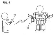
- the assist device of the present invention when utilized in order to perform risky operations, operations in circumstances where human operations are difficult, e.g., in particular circumstances such as outer space and deep ocean, the assist device can be operated in a safe place for a human body, so that safety of the human body can be maintained.
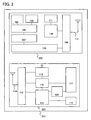
- an assist device 101 of the present invention includes a detecting portion 102 and an assist device driving portion 103.
- the detecting portion 102 includes a first sensor 100 which detects a biosignal, an amplifier circuit 106 which amplifies the detected biosignal, an A/D converter circuit 107 which converts the amplified signal into a digital signal, a central arithmetic processing circuit 108 which processes the signal, a transmitting/receiving circuit 109 for communicating with the assist device driving portion, an antenna 112, a battery 111 for driving these circuits, and a charging circuit 110 for charging the battery 111.
- the following can be used: embedding the detecting portion 102 in the body, putting the detecting portion 102 on the outside of the body so that detecting portion 102 is wrapped around a portion detecting a biosignal, incorporating the detecting portion 102 in a socket which connects the assist device driving portion 103 and the human body, and the like.
- the method for fixing the detecting portion 102 is not limited to the above-described modes.
- each of the amplifier circuit 106, the A/D converter circuit 107, the central arithmetic processing circuit 108, the transmitting/receiving circuit 109, the antenna 112, the battery 111, and the charging circuit 110 is thin and soft like a film and the implantable detecting portion 102 be covered with a material which is safe of the human body, such as silicon.
- a material which is safe of the human body such as titanium, platinum, or gold is preferably used as a metal which is necessary to be exposed to the detecting portion 102. Accordingly, the detecting portion 102 can be permanently put in the body.
- the assist device driving portion 103 can be easily changed in accordance with growth stages or applications.
- a junction between the detecting portion 102 and the assist device driving portion 103 is separated at a skin surface and data can be transmitted without using a connection terminal or the like, a connection terminal is not exposed and bathing, swimming, and wet work taking off the assist device driving portion 103 can be performed.
- corrosion, electric leakage, and the like can be prevented and there are advantages in beauty, infection prevention, and the like.
- the first sensor 100 is preferably provided at a position where the first sensor 100 can easily detect a biosignal which is to be detected.
- a biosignal which is to be detected for controlling the assist device driving portion 103 there are one or more of a myoelectric potential, a neural potential generated in accordance with an instruction to " move a certain portion of the body" which is issued from the brain, change in movement of a muscle or a tendon, pressure generated on a skin surface or in the body, speed, and an angle, and the like.
- a myoelectric potential electrode is used for the first sensor 100.
- a neural potential detecting element is used for the first sensor 100.
- a sensor which detects displacement is used for the first sensor 100.
- the sensor which detects displacement are a pressure sensor, an acceleration sensor, an angular velocity sensor, and a bending resistor. Since a weak signal can also be detected by using a MEMS for the sensor which detects displacement, the sensor which detects displacement is small and has high sensitivity.
- the amplifier circuit 106 When a signal detected by the first sensor 100 is input to the amplifier circuit 106, the amplifier circuit 106 amplifies the signal to a potential which is suitable for signal processing. Generally, the amplifier circuit 106 is formed using a circuit using differential amplification.
- the A/D converter circuit 107 is a circuit which converts a signal generated by the amplifier circuit 106 into a digital signal which can be used in the central arithmetic processing circuit 108.
- the central arithmetic processing circuit 108 provided in the detecting portion 102 performs pattern recognition based on a plurality of A/D converted digital signals; determines a series of operations of a joint included in the assist device driving portion 103, such as flection, extension, pronation, supination, abduction, and adduction, which is necessary for the user; and outputs a digital signal corresponding to the operation. Note that in order to realize a plurality of joint operations at the same time in the assist device driving portion 103, it is preferable that a signal having a plurality of channels be output at the same time.
- pattern recognition may be performed using a central arithmetic processing circuit 115 provided in the assist device driving portion 103. In this case, the central arithmetic processing circuit 108 provided in the detecting portion 102 is not necessary.
- the first sensor 100, the amplifier circuit 106, the A/D converter circuit 107, the central arithmetic processing circuit 108 provided in the detecting portion 102, the transmitting/receiving circuit 109, and the charging circuit 110 can be made smaller by being integrated and using CMOS transistor technology, they are suitable for being embedded in the body.
- the detecting portion 102 can be thinned, which is preferable.
- the transmitting/receiving circuit 109 provided in the detecting portion 102 includes circuits for wireless communication, such as a demodulation circuit 201, a decoding circuit 202, a logic arithmetic control circuit (a logic circuit) 203, a memory circuit 204, an encoding circuit 205, and a modulation circuit 206, and wirelessly communicates with the assist device driving portion 103.
- the transmitting/receiving circuit 109 provided in the detecting portion 102 includes a transmitting portion which transmits a signal having a single channel or a plurality of channels to the transmitting/receiving circuit 113 provided in the assist device driving portion 103, a receiving portion which receives an electromagnetic wave or an electric field from the transmitting/receiving circuit 113 provided in the assist device driving portion 103 and outputs it to the charging circuit 110, and the like.
- the transmitting portion performs phase shift keying of a digital signal having a plurality of channels and transmits the digital signal having the plurality of channels to the antenna 114 provided in the assist device driving portion 103 through the antenna 112 provided in the detecting portion 102 by an electromagnetic wave using orthogonal frequency division multiplexing.
- the transmitting portion can transmit digital signals using a coiled antenna for channels which are necessary for communication by an electromagnetic induction method.
- the transmitting portion can also perform optical communication.
- the detecting portion 102 and the assist device driving portion 103 are electrically separated as described above, safety of the user can be improved.
- communication can be performed through a skin using an infrared ray or the like.
- a transmitting/receiving circuit provided in a myoelectric potential detecting portion is preferably provided close under the skin.
- a transmission antenna and a reception antenna may be separately provided.
- the antenna 112 provided in the detecting portion 102 can perform transmission and reception using one antenna.
- the antenna may be mounted inside or on a surface of the detecting portion 102, or can be separately provided outside.
- a coiled antenna for channels which are necessary for transmission and reception of data can be provided.
- a light-emitting portion and a light-receiving portion for transmitting and receiving a signal for driving the assist device driving portion 103 are provided as well as a reception antenna for receiving an electromagnetic wave for generating power.
- the charging circuit 110 provided in the detecting portion 102 includes a rectifier circuit 207 which converts input AC current into DC current, a current-voltage control circuit (also referred to as a regulator) 208 which makes rectified power into voltage suitable for charging, a charging control circuit 209 which controls voltage output to the battery 111, and the like (see FIG. 4B ).
- a rectifier circuit 207 which converts input AC current into DC current
- a current-voltage control circuit also referred to as a regulator
- a charging control circuit 209 which controls voltage output to the battery 111, and the like (see FIG. 4B ).
- the detecting portion 102 in order to reduce a burden on the body to be embedded with the detecting portion 102, it is preferable that the detecting portion 102 be as small as possible.
- One of elements which determine the size of the detecting portion 102 is the battery 111. Since the battery 111 can be made smaller as power consumption of the detecting portion 102 is lower, a structure in which the number of signal processing performed by the central arithmetic processing circuit 108 provided in the detecting portion 102 is reduced and necessary signal processing is performed by the central arithmetic processing circuit 115 provided in the assist device driving portion 103 can be used, for example. Alternatively, a method can be employed in which the battery 111 of the detecting portion 102 is made smaller and charging is frequently performed at short time intervals.
- the assist device preferably has a function of saving power by stopping the detecting portion 102.
- a structure can be used in which an instruction to stop operations of the detecting portion 102 or an instruction to stop operations of the detecting portion 102 from the assist device detecting portion 103 can be given by determining whether the transmitting/receiving circuit 109 included in the detecting portion 102 and the transmitting/receiving circuit 113 included in the assist device driving portion 103 are in the range of a distance where communication can be performed.
- the transmitting/receiving circuit 109 of the detecting portion 102 receives an electromagnetic wave transmitted from the antenna 114 provided in the assist device driving portion 103 through the antenna 112 provided in the detecting portion 102, and outputs obtained AC current to the charging circuit 110.
- a structure can be used in which displacement current which is obtained by receiving change in magnetic flux generated from a coiled antenna provided in the assist device driving portion 103 by a coiled antenna provided in the detecting portion 102 is output to the charging circuit 110.
- the assist device 101 of the present invention includes the transmitting/receiving circuits for wireless communication and the wireless charging means (an RF battery) as described above, the assist device driving portion 103 and the detecting portion 102 can be electrically separated. In addition, conductive part of the detecting portion 102 can be made not to be exposed. Therefore, the assist device 101 of the present invention can be an assist device which is safe for the user and is water-resistant.
- a rechargeable secondary battery can be used for the battery 111 provided in the detecting portion 102.
- an electric-double layer capacitor having a collector electrode, a polarizable electrode, a separator, or an electrolytic solution can be used.
- an electrolytic solution and an electrode which are safe for the human body is preferably selected.
- the assist device driving portion 103 includes a driving portion 117 for operations, a drive control circuit 120 for driving and controlling the driving portion 117, a second sensor 200 for detecting pressure, temperature, or the like, a central arithmetic processing circuit 115 which processes a driving control signal, a signal from the sensor, or the like, a transmitting/receiving circuit 113 for receiving a signal from the detecting portion 102 and transmitting an electromagnetic wave for charging to the detecting portion 102, a battery 119 for driving the assist device driving portion 103, and a charging circuit 118 for charging the battery 119.
- the assist device driving portion 103 transmits power of the battery 119 wirelessly through the transmitting/receiving circuit 113. Therefore, the transmitting/receiving 113 preferably includes an oscillator for transmitting power in addition to the structure of the transmitting/receiving circuit 109 of the detecting portion 102.
- the assist device driving portion 103 includes a cover which entirely covers the assist device driving portion 103.
- the assist device driving portion 103 is connected to the assist device or the user by a socket using silicon.
- the assist device driving portion 103 is fixed by a known method, for example, by fixing the assist device driving portion 103 to the assist device or the user using a band.
- the driving portion 117 includes a driving mechanism having a skeleton and a joint, a wire, a sleeve, a motor for pressing and pulling the wire, an artificial muscle, and the like.
- a signal from the central arithmetic processing circuit 115 provided in the assist device driving portion 103 is input to the drive control circuit 120, and current and voltage which are necessary for operations of the motor or the artificial muscle of the driving portion 117 are generated.
- the second sensor 200 detecting pressure and temperature which are external stimuli may be provided on a surface of the assist device driving portion 103.
- a temperature sensor can detect temperature of an object which is touched by the assist device driving portion 103.
- a structure can also be used in which the risky condition of the assist device can be known by using warning indication using light or sound. Note that depending on applications of the assist device, a structure without a temperature sensor can be used.
- pressure applied to the assist device driving portion 103 can be detected.
- a sensor which is formed using MEMS (micro electro mechanical system) technology can be used, for example.
- MEMS micro electro mechanical system
- a sensor which is formed using MEMS technology is small, lightweight, and highly-sensitive. Therefore, weight of the assist device driving portion 103 can be reduced and movement of the assist device can be approximated to movement of real extremities.
- the transmitting/receiving circuit 113 provided in the assist device driving portion 103 includes a transmitting portion which transmits an electromagnetic wave or an electric field to the detecting portion 102, and a receiving portion which receives and demodulates the electromagnetic wave, the electric field, or light transmitted from the detecting portion 102, decodes the electromagnetic wave, the electric field, or light transmitted from the detecting portion 102 into a digital signal, and outputs the digital signal.
- the transmitting/receiving circuit 113 provided in the assist device driving portion 103 includes circuits for wireless communication, such as a demodulation circuit, a decoding circuit, a logic arithmetic control circuit (a logic circuit), a memory circuit, an encoding circuit, and a modulation circuit, and wirelessly communicates with the detecting portion 102.
- the transmitting portion of the transmitting/receiving circuit 113 transmits an electromagnetic wave using an antenna in order to charge the battery 111 of the detecting portion 102.
- the transmitting portion of the transmitting/receiving circuit 113 can transmit power using a coiled antenna by an electromagnetic induction method.
- a dipole antenna or a patch antenna is used by a radio wave method.
- the receiving portion of the transmitting/receiving circuit 113 can have a structure in which phase shift keying and decoding of a transmitted signal are performed using orthogonal frequency division multiplexing, and the signal is output to the central arithmetic processing circuit 115 as a digital signal having a plurality of channels.
- the receiving portion of the transmitting/receiving circuit 113 can have a structure in which demodulation and decoding of a transmitted signal are performed using a coiled antenna for channels which are necessary for communication by an electromagnetic induction method, and a digital signal having a plurality of channels is output to the central arithmetic processing circuit 115.
- the receiving portion of the transmitting/receiving circuit 113 can have a structure in which demodulation and decoding of an optical signal are performed, and a digital signal having a plurality of channels is output to the central arithmetic processing circuit 115.
- the assist device of the present invention can have a structure in which the assist device driving portion 103 and the detecting portion 102 communicate with each other using various methods.
- Data on a biosignal which is transmitted from the detecting portion 102 and is received by the transmitting/receiving circuit 113 provided in the assist device driving portion 103 is input to the central arithmetic processing circuit 115 provided in the assist device driving portion 103; the central arithmetic processing circuit 115 provided in the assist device driving portion 103 performs pattern recognition based on this data; and the central arithmetic processing circuit 115 provided in the assist device driving portion 103 determines a series of operations of a joint included in the assist device driving portion 103, such as flection, extension, pronation, supination, abduction, and adduction, which is necessary for the user.
- a signal is output to the drive control circuit 120.
- the arithmetic processing circuit 115 provided in the assist device driving portion 103 may have a learning function of pattern recognition.
- the arithmetic processing circuit 115 provided in the assist device driving portion 103 can have a function of learning based on the amount and an operation result of a biosignal input to the detecting portion 102, and determining a parameter which is suitable for the user of the assist device 101 to perform operations.
- the charging circuit 118 provided in the assist device driving portion 103 includes a rectifier circuit which converts AC current input from an external power supply into DC current, a current-voltage control circuit for making rectified power into a suitable value for charging, a charging control circuit which controls power supplied to the battery 119, and the like.
- the power input from the external power supply is stored in the battery 119 through the charging circuit 118.
- the battery 119 which is charged as described above supplies power to each part of the assist device driving portion 103 in order to drive the whole assist device driving portion 103.
- the battery 119 provided in the assist device driving portion 103 can also have a structure in which an electromagnetic wave which is transmitted from an external charger is received through the antenna 114 provided in the assist device driving portion 103, obtained AC current is output to the charging circuit 118 provided in the assist device driving portion 103 to change the battery 119 provided in the assist device driving portion 103.
- a structure can be used in which displacement current which is obtained by receiving change in magnetic flux generated from a coiled antenna included in the external charger by the coiled antenna provided in the assist device driving portion 103 is output to the charging circuit 118 provided in the assist device driving portion 103.
- the assist device driving portion 103 needs high power because it includes the driving portion 117 which includes the motor, the artificial muscle, or the like. However, it is preferable that the battery 119 provided in the assist device driving portion 103 be as lightweight as possible.
- the assist device driving portion 103 is water-resistant to some extent, such as covering the assist device driving portion 103 with a cover having rubber packing after unplugging the outlet.
- the assist device 101 When the assist device 101 is water-resistant as described above, danger of an electric shock or electric leakage is removed and quality of life of the user can be improved.
- a battery which is similar to the battery 111 of the detecting portion 102 can be used for the battery 119.
- a wireless charging means an RF battery
- the assist device driving portion 103 which has a high voltage portion and the detecting portion 102 which is in contact with a human body are electrically separated, so that the assist device which has high security can be provided.
- the assist device 101 since a connection terminal is not necessary by performing communication between the detecting portion 102 and the assist device driving portion 103 wirelessly, the assist device 101 which can be easily changed in accordance with growth stages or necessity can be provided.
- a myoelectric artificial limb 221 of the present invention includes a myoelectric potential detecting portion 222 and an artificial limb driving portion 223.
- the myoelectric potential detecting portion 222 includes a myoelectric potential electrode 104 which detects a myoelectric potential, a reference electrode 105 which detects noise other than the myoelectric potential, the amplifier circuit 106 which amplifies the detected myoelectric potential, the A/D converter circuit 107 which converts the amplified signal into a digital signal, the central arithmetic processing circuit 108 which processes the signal, the transmitting/receiving circuit 109 for communicating with the artificial limb driving portion, the antenna 112, the battery 111 for driving the circuits, and the charging circuit 110 for charging the battery.
- the following can be used: embedding the myoelectric potential detecting portion 222 in the body, putting the myoelectric potential detecting portion 222 on the outside of the body so that the myoelectric potential detecting portion 222 is wrapped around a portion detecting a myoelectric potential, incorporating the myoelectric potential detecting portion 222 in a socket which connects the artificial limb driving portion 223 and the body, and the like.
- the method for fixing the myoelectric potential detecting portion 222 is not limited to this mode.
- FIG. 3 shows an example in which the artificial limb driving portion 223 is embedded in an arm amputated at a forearm portion.
- the myoelectric potential detecting portion 222 When the myoelectric potential detecting portion 222 is embedded in the human body, a myoelectric potential is detected without involving a skin, and data processing of the detected signal is performed, even a small signal can be detected with high accuracy and a more complicated artificial limb can be controlled.
- the myoelectric potential detecting portion 222 When the myoelectric potential detecting portion 222 is attached to the body, in the case of detecting a myoelectric potential on a skin surface, the detected myoelectric potential corresponds to a myoelectric potential obtained by overlapping myoelectric potentials generated by a plurality of muscles which are close to the skin.
- the myoelectric potential detecting portion 222 in the case of embedding the myoelectric potential detecting portion 222 in the body, a myoelectric potential of a particular muscle can be detected, and there is a possibility that complicated and flexible movement of the artificial limb can be realized by comprehensively judging pieces of data on respective muscles.
- a polarized potential generated between a myoelectric potential electrode attached to the skin surface and an electrolyte such as sweat on the skin, or noise caused by vibration of an electrode wiring, or a fluorescent lamp, a home electric appliance, a machine tool, or the like which is around the electrode is mixed, which is inevitable.
- each of the amplifier circuit 106, the A/D converter circuit 107, the central arithmetic processing circuit 108, the transmitting/receiving circuit 109, the antenna 112, the battery 111, and the charging circuit 110 is thin and soft like a film and the implantable myoelectric potential detecting portion 222 be covered with a material which is safe for the human body, such as silicon.
- a material which is safe for the human body such as titanium, platinum, or gold can be used as a metal which is necessary to be exposed to the myoelectric potential detecting portion 222. Accordingly, the myoelectric potential detecting portion 222 can be permanently put in the body.
- the myoelectric potential detecting portion 222 is formed using any of the above-described materials, the artificial limb driving portion 223 can be easily changed in accordance with growth stages or applications.
- a terminal or the like is not exposed to the skin surface, bathing, swimming, and wet work taking off the artificial limb driving portion 223 can be performed.
- corrosion, electric leakage, and the like can be prevented and there are advantages in beauty, infection prevention, and the like.
- the myoelectric potential electrode 104 is preferably provided in a belly muscle which is close to a tendon of a muscle. This is because a myoelectric potential is generated from the central of a muscle toward tendons at opposite ends.
- the reference electrode 105 has a function of removing noise or a signal which is mixed into a myoelectric potential detected by the myoelectric potential electrode 104. Since it is necessary to detect an object which is similar to such a signal or noise adversely affecting detection of a myoelectric potential by the reference electrode 105, the reference electrode 105 is preferably provided near a muscle which is to be detected and in a joint, a tendon, or the like which has less influence by the myoelectric potential.
- Circuits which are similar to those of Embodiment Mode 1 can be used for the amplifier circuit 106, the A/D converter circuit 107, the central arithmetic processing circuit 108 provided in the myoelectric potential detecting portion 222, the transmitting/receiving circuit 109, and the charging circuit 110. Since the amplifier circuit 106, the A/D converter circuit 107, and the central arithmetic processing circuit 108 provided in the myoelectric potential detecting portion 222, can be made smaller by being integrated and using CMOS transistor technology, they are suitable for being embedded in the body. When an n-channel thin film transistor and a p-channel thin film transistor are used for a CMOS transistor, the myoelectric potential detecting portion 222 can be thinned, which is preferable.
- a transmission antenna and a reception antenna may be separately provided.
- the antenna 112 provided in the myoelectric potential detecting portion 222 can perform transmission and reception using one antenna.
- the antenna may be mounted inside or on a surface of the myoelectric potential detecting portion 222, or can be separately provided outside.
- a coiled antenna for channels which are necessary for transmission and reception of data can be provided.
- a reception antenna for receiving a radio wave for power is provided.
- Circuits which are similar to the charging circuit 110 and the transmitting/receiving circuit 109 described in Embodiment Mode 1 can be used for the charging circuit 110 and the transmitting/receiving circuit 109 provided in the myoelectric potential detecting portion 222.
- the myoelectric artificial limb 221 of the present invention includes the transmitting/receiving circuits for wireless communication and the wireless charging means (an RF battery) as described above, the artificial limb driving portion 223 and the myoelectric potential detecting portion 222 can be electrically separated. In addition, conductive part of the myoelectric potential detecting portion 222 can be made not to be exposed. Therefore, the myoelectric artificial limb 221 of the present invention can be an artificial limb which is safe for the user and is water-resistant.
- a rechargeable secondary battery can be used for the battery 111 provided in the myoelectric potential detecting portion 222.
- an electric-double layer capacitor having a collector electrode, a polarizable electrode, a separator, or an electrolytic solution can be used.
- an electrolytic solution or an electrode which is safe for the human body is preferably selected.
- the artificial limb driving portion 223 includes the driving portion 117 for operations, the drive control circuit 120 for driving and controlling the driving portion 117, a varied sensor 116 for detecting pressure, temperature, or the like, the central arithmetic processing circuit 115 which processes a driving control signal, a signal from the sensor, or the like, the transmitting/receiving circuit 113 for receiving a signal from the myoelectric potential detecting portion 222 and transmitting an electromagnetic wave for charging to the myoelectric potential detecting portion 222, the battery 119 for driving the artificial limb driving portion 223, and the charging circuit 118 for charging the battery 119.
- the artificial limb driving portion 223 includes a cover which covers all the artificial limb driving portion 223.
- the artificial limb driving portion 223 is connected to an extremity stump portion by a socket using silicon and is fixed to the body of the user by a known method such as fixing the artificial limb driving portion 223 to an upper extremity or an lower extremity using a band.
- the artificial limb driving portion 223 is preferably fixed so that it does not disturb operation of the artificial limb and other portions.
- the driving portion 117 includes a driving mechanism having a skeleton and a joint, a wire, a sleeve, a motor for pressing and pulling the wire, an artificial muscle, and the like.
- a mechanism which is similar to driving of an actual limb for the driving mechanism.
- a tendon runs inside of a synovial sheath in a finger portion of an actual limb, and the tendon stops at a proximal phalanx, a middle phalanx, a distal phalanx, and a sheath of each finger depending on functions of the tendon. Then, the tendon moves when each muscle stretches, and each joint connected to the tendon moves.
- a method can be used in which a cable which is fixed to each finger of the driving mechanism is inserted inside of a lubricated sleeve, and each joint of the driving mechanism is driven by pressing and pulling the cable by a motor or an artificial muscle, for example.
- each joint of the driving mechanism is driven using a cable
- the number of motors can be reduced and degree of freedom which is more than the number of motors can be realized because it is not necessary to provide a motor in each joint.
- power consumption and weight can be reduced.
- an actuator which is formed using a high molecule can be used for the artificial muscle.
- the artificial muscle power consumption and weight can be further reduced compared with the case of using the motor.
- the sensor 116 detecting pressure and temperature which are external stimuli may be provided on a surface of the artificial limb driving portion 223.
- a temperature sensor can detect temperature of an object which is touched by the artificial limb driving portion 223.
- a structure can also be used in which the user of the myoelectric artificial limb 221 can know temperature around the artificial limb driving portion 223 by a method of reproducing a sense on a skin surface such as an extremity stump portion using a heater, applying an appropriate stimulus to a sensory nerve, or the like.
- a structure can also be used in which the user of the artificial limb can know the risky condition by using warning indication using light or sound. Note that depending on applications of the artificial limb, a structure without a temperature sensor can be used.
- pressure applied to the artificial limb device driving portion 223 can be detected.
- a human performs operations of grasping and picking using a hand
- hardness and elasticity of an object to be grasped are predicted based on sight, experience, and the like, and pressure which should be applied to a finger is determined.
- a muscle moves while always feeding back data on whether the hand touches an object or how much pressure is applied to the object by a tactile sense of the finger, i.e., pressure.
- the artificial limb driving portion 223 can have a structure in which data on a tactile sense is given to the user of the artificial limb by stimulating a sensory nerve based on data obtained by the pressure sensor.
- a structure can be employed in which excess and deficiency of grip force at the time of an operation such as grip are adjusted depending on operation patterns of the user of the artificial limb.
- the amount of adjustment is determined by the central arithmetic processing circuit 115 provided in the artificial limb driving portion 223.
- the present invention is not limited to this mode, and the amount of adjustment may be determined by the central arithmetic processing circuit 108 provided in the myoelectric potential detecting portion 222 or the like.
- a sensor which is formed using MEMS (micro electro mechanical system) technology can be used, for example.
- MEMS micro electro mechanical system
- a sensor which is formed using MEMS technology is small, lightweight, and highly-sensitive. Therefore, weight of the artificial limb driving portion 223 can be reduced, a thin finger can be realized, and movement of the myoelectric artificial limb can be approximated to movement of real extremities.
- the drive control circuit 120, the transmitting/receiving circuit 113, the charging circuit 118, and the battery 119 provided in the artificial limb driving portion 223 can be used similarly to Embodiment Mode 1.
- a receiving portion of the transmitting/receiving circuit 113 has a structure in which phase shift keying and decoding of a transmitted signal are performed using orthogonal frequency division multiplexing, and the signal is output to the central arithmetic processing circuit 115 as a digital signal having a plurality of channels.
- the receiving portion of the transmitting/receiving circuit 113 can have a structure in which demodulation and decoding of a transmitted signal are performed using a coiled antenna for channels which are necessary for communication using an electromagnetic induction method, and a digital signal having a plurality of channels is output to the central arithmetic processing circuit 115.
- the receiving portion of the transmitting/receiving circuit 113 can have a structure in which demodulation and decoding of an optical signal are performed, and a digital signal having a plurality of channels is output to the central arithmetic processing circuit 115.
- the myoelectric artificial limb of the present invention can have a structure in which the artificial limb driving portion 223 and the myoelectric potential detecting portion 222 communicate with each other using various methods.
- Data on a myoelectric potential which is transmitted from the myoelectric potential detecting portion 222 and is received by the transmitting/receiving circuit 113 provided in the artificial limb driving portion 223 is input to the central arithmetic processing circuit 115 of the artificial limb driving portion 223; the central arithmetic processing circuit 115 of the artificial limb driving portion 223 performs pattern recognition based on this data; and the central arithmetic processing circuit 115 of the artificial limb driving portion 223 determines a series of operations of a joint included in the artificial limb driving portion 223, such as flection, extension, pronation, supination, abduction, and adduction, which is necessary for the user.
- a signal is output to the drive control circuit 120.
- data from the sensor 116 such as the temperature sensor, the pressure sensor, or the like provided in the artificial limb driving portion 223 is input to the central arithmetic processing circuit 115 of the artificial limb driving portion 223; the central arithmetic processing circuit 115 of the artificial limb driving portion 223 judges intention of the user of the artificial limb such as grasping or picking by a result of pattern recognition; and the central arithmetic processing circuit 115 of the artificial limb driving portion 223 adjusts power generated by the motor or the artificial muscle when needed.
- the arithmetic processing circuit 115 provided in the artificial limb driving portion 223 may have a learning function of pattern recognition.
- the arithmetic processing circuit 115 provided in the artificial limb driving portion 223 can have a function of learning based on the amount and an operation result of a myoelectric potential input to the myoelectric potential detecting portion 222, determining a parameter which is suitable for the user of the artificial limb to perform operations.
- the charging circuit 118 provided in the artificial limb driving portion 223 includes a rectifier circuit which converts AC current input from an external power supply into DC current, a current-voltage control circuit for making rectified power into a suitable value for charging, a charging control circuit which controls power supplied to the battery 119, and the like.
- the power input from the external power supply is stored in the battery 119 through the charging circuit 118.
- the battery 119 which is charged as described above supplies power to each part of the artificial limb driving portion 223 in order to drive the whole artificial limb driving portion 223.
- the battery 119 provided in the artificial limb driving portion 223 can also have a structure in which an electromagnetic wave which is transmitted from an external charger is received through the antenna 114 provided in the artificial limb driving portion 223, obtained AC current is output to the charging circuit 118 provided in the artificial limb driving portion 223 to change the battery 119 provided in the artificial limb driving portion 223.
- a structure can be used in which change in magnetic flux generated from a coiled antenna included in the external charger is received by the coiled antenna provided in the artificial limb driving portion 223, and the received displacement current is output to the charging circuit 118 provided in the artificial limb driving portion 223.
- the artificial driving portion 223 needs high power because it includes the driving portion 117 which includes the motor, the artificial muscle, or the like. However, it is preferable that the battery 119 provided in the artificial limb driving portion 223 be as lightweight as possible.
- the myoelectric potential detecting portion 222 which is to be embedded in the body is preferably as small as possible in order to reduce a burden on the body to be embedded with the myoelectric potential detecting portion 222.
- One of elements which determine the size of the myoelectric potential detecting portion 222 can be the battery 111. Since the battery 111 can be made smaller as power consumption of the myoelectric potential detecting portion 222 is lower, a structure in which the number of signal processing performed by the central arithmetic processing circuit 108 provided in the myoelectric potential detecting portion 222 is reduced and necessary signal processing is performed by the central arithmetic processing circuit 115 provided in the artificial limb driving portion 223 can be used, for example. Alternatively, a method can be employed in which the battery 111 of the myoelectric potential detecting portion 222 is made smaller and charging is frequently performed at short time intervals.
- the artificial limb preferably has a function of saving power by stopping the myoelectric potential detecting portion 222.
- a structure can be used in which an instruction to stop operations of the myoelectric potential detecting portion 222 or an instruction to stop operations of the myoelectric potential detecting portion 222 from the artificial limb detecting portion 223 can be given by determining whether the transmitting/receiving circuit 109 included in the myoelectric potential detecting portion 222 and the transmitting/receiving circuit 113 included in the artificial limb driving portion 223 are in the range of a distance where communication can be performed.
- the myoelectric artificial limb 221 When the myoelectric artificial limb 221 is water-resistant as described above, danger of an electric shock or electric leakage is removed, bathing, swimming, sports with sweating, and the like while putting on the myoelectric artificial limb 221 can be performed, and quality of life of the user can be improved.
- a potential detected by the myoelectric potential electrode 104 of the myoelectric potential detecting portion 222 is amplified by the amplifier circuit 106 and the detected potential is converted into a digital signal by the A/D converter circuit 107, a series of operations of a joint included in the artificial limb driving portion 223 is determined by the central arithmetic processing circuit 108, and a digital signal corresponding to the operation is output.
- the transmitting/receiving circuit 109 modulates the digital signal and transmits the modulated digital signal to the antenna 114 provided in the artificial limb driving portion 223 through the antenna 112 provided in the myoelectric potential detecting portion 222 using an electromagnetic wave.
- a signal transmitted from the myoelectric potential detecting portion 222 is received by the transmitting/receiving circuit 113 through the antenna 114.
- data on a myoelectric potential which is transmitted from the myoelectric potential detecting portion 222 and is received by the transmitting/receiving circuit 113 is input to the central arithmetic processing circuit 115; pattern recognition is performed based on this data; and a series of operations of a joint included in the artificial limb driving portion 223, such as flection, extension, pronation, supination, abduction, and adduction, which is necessary for the user, is determined.
- the drive control circuit 120 generates current and voltage which are necessary for operations of the motor or the artificial limb of the driving portion 117 from the central arithmetic processing circuit 115 provided in the artificial limb driving portion 223.
- the driving portion 117 includes a skeleton, a joint mechanism, and a driving mechanism.
- the driving portion 117 may include a protective cover.
- the skeleton corresponds to a human bone.
- the joint mechanism corresponds to a human joint. Therefore, the joint mechanism is provided between skeletons (there is the case in which an end of a skeleton functions as the joint mechanism).
- the driving mechanism corresponds to a human muscle.
- the driving mechanism uses a motor or an artificial muscle as a power source.
- the amount and the speed of movement of the motor or the artificial muscle are controlled by the drive control circuit 120.
- the case in which the driving portion is driven mainly using a motor is described.
- Silicon rubber may be used for the protective cover for beauty, dust prevention, water resistance, insulation, or the like.
- plastic can be used for lightweight, and these materials can be used properly depending on purposes.
- FIGS. 11 to 14 structures of the driving portion 117 are described with reference to FIGS. 11 to 14 using simple models.
- the driving portion 117 is a model having an opening and closing mechanism for sandwiching an object.
- FIG 11 is a perspective view of the driving portion 117.
- FIGS. 12A and 12B are top views of the driving portion 117.
- FIG 13 is a diagram of the joint mechanism.
- the driving portion 117 includes a movable skeleton 311, a fixed skeleton 312, wires 313a and 313b, and a driving portion 316.
- the movable skeleton 311 and the fixed skeleton 312 include a joint mechanism 319 so that ends of respective skeletons are combined with each other and can move (therefore, in this case, part of the skeletons forms the joint mechanism).
- the driving portion drives the fixed skeleton 312 by the driving mechanism and the joint mechanism so that the movable skeleton 311 opens and closes.
- the joint mechanism 319 is provided so that the movable skeleton 311 and the fixed skeleton 312 are combined like a hinge. Therefore, movable skeleton-side joint holes 321 and a fixed skeleton-side joint hole 322 are provided at the end of the movable skeleton and the end of the fixed skeleton, respectively, and the joint mechanism includes a pin 323 which is to pass through these joint holes.
- an uniaxial operation an opening and closing operation
- the movable skeleton 311 includes wire fixing tools 314, and the movable skeleton 311 and the fixed skeleton 312 include wire drawing-in pipes 317 and 318 for passing the wire inside.
- the wire can be provided not inside the skeletons but outside the skeletons and driving can be performed. In that case, wire drawing-in pipes are not necessary. Further, in that case, wire fixing tools may also be provided outside the skeletons. In this embodiment mode, an example in which a wire is provided inside the skeletons is shown.
- the driving portion 316 includes two wires 313a and 313b and the wires 313a and 313b are connected to the above-described two wire fixing tools 314.
- the movable skeleton 311 and the fixed skeleton 312 include the wire drawing-in pipes 317 and 318 for passing the two wires 313a and 313b.
- the wires 313a and 313b fixed to the wire fixing tools 314 of the movable skeleton 311 pass inside the fixed skeleton 312 through the joint mechanism and are connected to the driving portion 316.
- the driving portion 316 includes a pulley 331, a spring 332, a gear 333, a worm gear 334, a motor 335, and the like.
- a position where the driving mechanism is provided is not limited, an example in which the driving portion 316 is provided in the fixed skeleton 312 is shown in this embodiment mode.
- the driving portion 316 can be made smaller.
- the wires 313a and 313b which pass through the movable skeleton 311 and the fixed skeleton 312 are wound around the pulley 331. Ends of the wires 313a and 313b are connected to the spring 332.
- the spring 332 is fixed inside the fixed skeleton 312 (when likening to a muscle included in the human body, the spring 332 is fixed to an origin of a flexor and an extensor)
- FIG 12 B shows a view in which the wire 313b is wound around the pulley 331, the wire 313a is wound around another pulley 331 similarly.
- the spring 332 prevents the wires 313a and 313b from slack and being pulled firmly of by tension of the spring 332. Therefore, in the case where a driving portion which performs simple operations is acceptable, a spring is not necessary and an end of a wire which is wound around the pulley may be directly fixed to the fixed bone 312. However, when a wire is fixed through a spring, a margin can be given to an operation of flection or extension, so that more favorable movement can be realized.
- the pulley 331 is fixed to the gear 333 and the gear 333 engages with worm gear 334.
- the worm gear 334 is fixed to the motor 335.
- rotation of the motor 335 is transmitted to rotation of the pulley 331, and the wires 313a and 313b can be pulled and loosened.
- the movable skeleton 311 can be moved. For example, as shown in FIGS. 14A and 14B , when the wire 313b fixed to the inside wire fixing tool is pulled, the movable skeleton 311 moves so as to be in contact with the fixed skeleton 312 side, i.e., performs a picking operation. In addition, when the wire 313a fixed to the outside wire fixing tool is pulled, the movable skeleton 311 moves so as to be separate from the fixed skeleton 312, i.e., performing an opening operation.
- the movable skeleton 311 opens in a direction which is opposite to gravity, and the movable electrode 316 closes without application of force for opening, only a wire for opening (the wire fixed to the outside wire fixing tool) can be provided.
- driving may be performed using two wires; however, by fixing one of operations as described above and having a structure of an operation such as performing or not performing an opposite operation, the wires and the driving mechanism can be collected. Therefore, the number of components of the driving portion can be reduced, so that the driving portion can be reduced in size and weight.
- the assist device of the present invention is used as a human artificial limb.
- a simple uniaxial operation such as opening and closing is performed.
- a human's hand performs complicated and delicate operations such as holding, picking, pressing a button, and the like.
- the assist device 101 of the present invention is used as a driving portion of an artificial limb having a skeleton which is close to a human bone, i.e., an artificial limb which can reproduce movement of the limb is described below.
- each part forming the skeleton is referred to as " ⁇ skeleton".
- ⁇ skeleton a name of each part forming the skeleton " ⁇ skeleton” corresponds to a name of the human bone " ⁇ bone”.
- the driving portion 117 includes a skeleton, a joint mechanism, a driving mechanism, a wire, and the like, similarly to the above-described example.
- An actual limb includes 19 movable bones, and thus complicated operations of the limb can be realized. It is preferable that a hand portion of the driving portion 117 include 19 movable skeletons similarly to an actual bone also in this example.
- the skeleton includes a skeleton of a hand 410 forming five fingers (the skeleton of the hand 410 includes distal skeletons 412, middle skeletons 413, finger skeletons 411 formed from proximal skeletons 414, and metacarpal skeletons 415.
- a finger skeleton of a first finger is formed of the distal skeleton and the proximal skeleton
- an artificial hand proximal skeleton 420 which is connected the skeleton of the hand 410 through the joint mechanism.
- the finger skeletons 411 and the artificial hand proximal skeleton 420 may be covered with a cover 427.
- a socket 428 which connects the artificial limb driving portion 223 and the human body is provided.
- skeletons are preferably formed using materials which are lightweight and have high durability such as plastic and titanium in order to lighten the assist device and realize nimble operability.
- materials which are lightweight and have high durability such as plastic and titanium in order to lighten the assist device and realize nimble operability.
- the present invention is not limited to these materials.
- the finger skeletons 411 corresponding to a plurality of fingers may be collected into one wide skeleton.
- a structure can be used in which finger skeleton of second to fifth fingers and the metacarpal skeleton are collected and the first finger is independent like a mitten.
- each of the proximal skeletons 414 and the metacarpal skeletons 415 has a columnar shape having the length and a diameter based on each of finger skeletons and metacarpal skeletons. Since an actual finger becomes thinner as an end, each of these skeletons preferably has a columnar shape which becomes thinner as an end.
- each of the finger skeletons and the metacarpal skeletons has the hinge structure described in the above-described example to form a joint mechanism using adjacent skeletons. Note that a joint mechanism is not provided at ends of the distal skeletons (in the diagram, the joint mechanism of the finger skeleton and the like are omitted).
- the joint mechanism of the hinge structure is provided between each of the finger skeletons and the metacarpal skeletons as described above, operations corresponding to flection and extension of a finger can be performed.
- each of the distal skeletons 412 may have a shape in which thickness becomes thinner toward the end.
- a gap for providing a sensor is formed at an end (i.e., a finger tip) of the driving portion 117 and an actual finger has such a structure, which is good for appearance.
- the metacarpal skeletons 415 are located inside of a palm of the artificial hand, the length thereof is not necessarily based on the length of metacarpal bones. Therefore, the length of the metacarpal skeletons is shorter than the length of metacarpal bones, and in a gap therebetween, a joint mechanism between each of the finger skeletons 411 and the carpal skeleton 422, and a driving mechanism for driving each of the finger skeletons 411 can be provided.
- the first finger and the second to fifth fingers have different movable directions and the like.
- the joint mechanism between each of the finger skeletons 411 and the carpal skeleton 422 includes a first joint mechanism provided between a middle finger skeleton of the first finger and the carpal skeleton and a second joint mechanism provided between middle finger skeletons of the second to fifth fingers and the carpal skeleton.
- the first finger Since the first finger performs a rotation operation unlike other fingers, the first finger includes a driving mechanism which drives the first finger through the first joint mechanism.
- a driving mechanism which performs an operation of opening a hand (specifically, an operation of opening the second finger to the first finger side and opening the fourth and fifth finger to the outside of the fifth finger) can be provided.
- this driving mechanism can be formed using a fixed axis of the finger skeleton, a spring for suppressing natural opening of the finger skeleton, a gear engaging with a gear fixed to the metacarpal skeleton, a motor fixed to the gear, and the like.
- a structure can be used in which such a shape of the hand is formed by a shape of the skeleton of the hand and such a driving mechanism is not provided.
- the artificial hand proximal skeleton 420 includes a carpal skeleton 422 which is connected to a joint mechanism 421, a forearm skeleton 424 which is connected to the carpal skeleton 422 through a joint mechanism 423, and a brachio skeleton 426 which is connected to the forearm skeleton 424 through a joint mechanism 425.
- the carpal skeleton 422 can be formed using one skeleton.
- the present invention is not limited to this, and the carpal skeleton 422 may be formed using two or more skeletons.
- an actual forearm bone can perform a pronation operation, a supination operation, and the like by including two bones of a radius and an ulna
- the forearm skeleton 424 can be formed using one skeleton because the driving portion 117 can compensate a pronation operation, a supination operation, and the like by the joint mechanism or the driving mechanism.
- the structure in which the driving portion 117 includes skeletons up to the brachio skeleton 426 in this example needless to say, a brachio skeleton is not necessary when the user of the artificial limb only needs skeletons beyond a forearm.
- a joint there are a uniaxial hinge joint, a biaxial saddle joint, a triaxial carpal joint, and the like depending on functions. Since all the joints of second to fifth fingers and a finger joint of a first finger are uniaxial movements of extension in an actual hand, a joint mechanism of a hinge structure is provided between skeletons thereof.
- a joint of a root of the first finger (a joint between a metacarpal bone and a carpal bone of the first finger) includes a biaxial saddle joint in which orthogonal movement is added to movement of a hinge joint, unlike other fingers. Therefore, a joint mechanism between the metacarpal skeleton and the carpal skeleton of the first finger realizes movement which is similar to that of the actual first finger by including a hinge joint at upper part as a joint according to the biaxial saddle joint and a hinge joint which is orthogonal to it at lower part, or including a joint mechanism of a rotational structure.
- An joint structure having such multi-axial movement is similar to the joint mechanism 423 between the carpal skeleton 422 and the forearm skeleton 424 and the joint mechanism 425 between the forearm skeleton 424 and the brachio skeleton 426.
- Each of the skeletons realizes movement of a joint by pulling (or loosening) a wire passing through the inside. Running and a power source of the wire are described below.
- the distal skeletons 412 includes two wire drawing-in pipes for passing wires inside and wire fixing tools for fixing the wires around the center of the inside of the distal skeletons 412.
- the wire fixing tools are provided on the palm side and the back of the hand side, respectively (when likening to a muscle included in the human body, the wire fixing tools are provided at stop positions of a flexor and an extensor).
- the middle skeletons 413 also include two wire drawing-in pipes and wire fixing tools. However, since extension of the middle skeletons 413 can be substituted for extension of the distal skeletons 412, the middle skeletons 413 can have a structure in which wire fixing tools are included only at a position corresponding to a muscle stop portion on the flexor side.
- each of the proximal skeletons 414 and the metacarpal skeletons 415 include three wire drawing-in pipes and wire fixing tools.
- the plurality of wires fixed to each of the skeletons as described above are connected to the driving mechanism through each of the finger skeletons and the wire drawing-in pipes provided in the metacarpal skeletons 415.
- each of the wires connected to the driving mechanism is rolled up by the pulley, the end thereof is connected to the spring, and the spring is fixed to inside or around the metacarpal skeletons 415 or the carpal skeleton 422 (when likening to the human body, the spring is fixed to an origin of each muscle or around the origin of each muscle).
- a structure without the spring may be used.
- the pulley is fixed to the gear and the gear engages with the worm gear.
- the worm gear is fixed to the motor through a shaft.
- each finger When the wire fixed to the wire fixing tool located at an extensor stop portion is pulled, each finger is bent. Then, when the wire fixed to the wire fixing tool located at the extensor stop portion is pulled, each finger is extended.
- This fixing structure of the wire is similar to the case of driving the artificial hand proximal skeleton.
- the metacarpal skeleton of the first finger needs to rotate in order to perform an operation of picking an object, or the like.
- the driving mechanism which drives the joint mechanism has a rotational axis and a pin of the rotational axis engages with a groove provided in a motor bearing.
- the driving mechanism is fixed.
- the assist device having a function as an artificial hand can be driven.
- the gear and the worm gear preferably has a structure with a little backlash as much as possible (here, a backlash corresponds to a gap between a screw and a gear at the time of dealing a machine. Since this gap is provided, the screw and the gear can freely move. However, when the machine rotates in a certain direction to a reverse direction, there is a possibility that misalignment in size is caused due to the backlash).
- a cog of the gear may be a rotational roller.
- the motor preferably has high positional accuracy, and for example, a stepping motor may be used.
- the driving portion 117 which is driven by passing a wire inside of the skeleton and pulling or loosening it is shown.
- the wire for driving each of the skeletons can be provided on the surface of each of the skeletons.
- an artificial muscle can be used for driving each of the skeletons.
- An artificial muscle contracts by a stimulus such as an electric stimulus or pressure and behaves similarly to a human's muscle.
- an artificial muscle is formed using a conductive high molecule or the like which contracts by voltage application.
- the driving mechanism and the wire can be replaced with this artificial muscle. It is acceptable as long as the artificial muscle is fixed to the origin of the muscle, around the origin of the muscle, or a stop portion of the muscle, similarly to the human's muscle.
- the drive control circuit 120 controls movement of the driving mechanism or the artificial limb by receiving a signal output from the central arithmetic processing circuit 115 provided in the artificial limb driving portion 223 shown in FIG. 2 . Specifically, the drive control circuit 120 generates current and voltage which are necessary for driving the motor included in the driving mechanism shown in FIG. 15 or the artificial muscle.
- first to fifth fingers are described in the upper limb
- first to fifth toes are described in the lower limb.
- the first to fifth toes include finger skeletons and metatarsal skeletons similarly to the skeletons which form the first to fifth fingers, and the metatarsal skeletons are connected to tarsal skeletons through the joint mechanism.
- the tarsal skeletons are connected to crural skeletons through the joint mechanism, and the crural skeletons are connected to femoral skeletons through the joint mechanism.
- an actual crural skeleton includes two bones of a tibial bone and a fibula
- a crural skeleton which forms the driving portion can be formed using one skeleton.
- a structure in which the driving portion includes up to the femoral skeleton is shown in this example, needless to say, a femoral skeleton is not necessary when the user of the artificial limb only needs skeletons beyond a crural skeleton.
- the lower limb includes similar bones to the upper limb, the lower limb does not perform complicated movement compared to the upper limb. Therefore, the structure of the lower limb can be simplified by collecting the bones which form the crus.
- the tarsal skeletons can be formed using one bone (similarly to the carpal skeleton).
- the metatarsal skeletons may be formed using one skeleton.
- the assist device there are a plurality of joints between metatarsal bones and tarsal bones and it is considered that the plurality of joints have important functions for maintaining balance at the time of standing or walking.
- a structure may be used in which the metatarsal skeletons and the tarsal skeletons are formed using a plurality of skeletons and movement of actual bones can be recreated.
- the lower limb can be driven by the wires, the driving mechanism which pulls and loosens the wires, and the joint mechanism provided between the respective skeletons, similarly to the upper limb.
- One end of a wire which substitutes main movement of a muscle is fixed to a stop portion of the muscle, and the other end thereof is fixed to the origin of the muscle through the driving mechanism.
- the joint mechanism provided between the respective skeletons includes uniaxial to triaxial joint mechanism in accordance with each of the joints.
- the myoelectric artificial limb 221 functioning as the upper extremity or the lower extremity can be provided.
- a wireless charging means an RF battery
- power charged in the battery of the artificial limb driving portion 223 can be supplied to the myoelectric potential detecting portion 222 wirelessly. Therefore, the artificial limb driving portion 223 which has a high voltage portion and the myoelectric potential detecting portion 222 which is in contact with a human body are electrically separated, so that the myoelectric artificial limb 221 which has high security can be provided. Further, in the present invention, since connection without using a terminal can be performed by unwiring communication between the myoelectric potential detecting portion 222 and the artificial limb driving portion 223, the myoelectric artificial limb 221 which can be easily changed in accordance with growth stages or applications can be provided.
- an application mode of an assist device which is different from that of Embodiment Mode 2, is described.
- a mode in which remote control of the assist device driving portion can be performed even when a distance between a detecting portion and the assist device driving portion is far is described with reference to FIGS. 1 and 5 .
- the detecting portion 102 is provided in extremities of the user.
- the assist device driving portion 103 is provided in extremities of a driving device (a robot) in which remote control can be performed.
- the first sensor of the detecting portion 102 detects movement of the extremities as a biosignal.
- the biosignal is processed by the amplifier circuit 106, the A/D converter circuit 107, and the central arithmetic processing circuit 108 provided in the detecting portion.
- the processed signal is transmitted from the transmitting/receiving circuit 109 to the assist device driving portion 103 through the antenna 112.
- the signal transmitted from the detecting portion 102 is received by the transmitting/receiving circuit 113 through the antenna 114.
- the signal received by the transmitting/receiving circuit 113 is processed by the central arithmetic processing circuit 115 and the drive control circuit 120 similarly to Embodiment Mode 1, so that the driving portion 117 can be driven.
- power which is obtained from an external power supply or a battery by the assist device driving portion 103 can be supplied to the detecting portion 102.
- the power which is obtained from the external power supply or the battery by the assist device driving portion 103 is transmitted to the detecting portion 102 through the transmitting/receiving circuit 113 and the antenna 114 of the assist device driving portion 103.
- the signal transmitted from the assist device driving portion 103 is received by the transmitting/receiving circuit 109 through the antenna 112.
- the signal received by the transmitting/receiving circuit 109 is processed by the charging circuit 110 similarly to Embodiment Mode 1, so that the battery 111 can be charged.
- the detecting portion 102 does not need a cord from the external power, a cord which is necessary for exchanging signals with the assist device or conveying electromagnetic waves, or the like, so that the detecting portion 102 can be cordless. Accordingly, the detecting portion 102 can be easily used.
- the assist device driving portion 103 can be controlled with high accuracy. Even when a distance between the detecting portion 102 and the assist device driving portion 103 is far, remote control of the assist device driving portion 103 can be performed using a communication repeater.
- the assist device driving portion 103 of the assist device 101 of the present invention when the assist device driving portion 103 of the assist device 101 of the present invention is provided in part of or all the extremities of a robot and in the body of the user of the detecting portion 102, remote control of the assist device driving portion 103 can be performed.
- the assist device driving portion 103 in order to perform operations in particular circumstances such as outer space and deep ocean, risky operations, or the like, can be used as a robot (see FIG 5 ).
- the detecting portion of the assist device can be formed by using a field effect transistor using a semiconductor substrate or an SOI substrate, a structure in which an antenna, a charging circuit, and a transmitting/receiving circuit are provided over the same substrate is described in this embodiment mode.
- a separation layer 1903 is formed over one surface of a substrate 1901 with an insulating film 1902 interposed therebetween.
- an insulating film 1904 functioning as a base film and a semiconductor film 1905 are stacked. Note that the insulating film 1902, the separation layer 1903, the insulating film 1904, and the semiconductor film 1905 can be sequentially formed.
- the substrate 1901 is selected from a glass substrate, a quartz substrate, a metal substrate (e.g., a stainless steel substrate), a ceramic substrate, a semiconductor substrate such as a silicon substrate, or the like.
- a substrate formed using polyethylene terephthalate (PET), polyethylene naphthalate (PEN), polyether sulfone (PES), acryl, or the like can be selected as a plastic substrate.
- PET polyethylene terephthalate
- PEN polyethylene naphthalate
- PES polyether sulfone
- the separation layer 1903 is provided over the entire surface of the substrate 1901 with the insulating film 1902 interposed therebetween; however, when needed, the separation layer 1903 may be selectively provided by photolithography after the separation layer is formed over the entire surface of the substrate 1901.
- the insulating film 1902 and the insulating film 1904 are formed by using an insulating material such as silicon oxide, silicon nitride, silicon oxynitride, or silicon nitride oxide by CVD, sputtering, or the like.
- an insulating material such as silicon oxide, silicon nitride, silicon oxynitride, or silicon nitride oxide by CVD, sputtering, or the like.
- a silicon nitride oxide film may be formed as a first layer
- a silicon oxynitride film may be formed as a second layer.
- a silicon nitride film may be formed as the first layer and a silicon oxide film may be formed as the second layer.
- the insulating film 1902 functions as a blocking layer which prevents an impurity element from being mixed into the separation layer 1903 or an element formed thereover from the substrate 1901.
- the insulating film 1904 functions as a blocking layer which prevents an impurity element from being mixed into an element formed over the separation layer 1903 from the substrate 1901 and the separation layer 1903.
- a metal film, a stacked-structure of a metal film and a metal oxide film, or the like can be used for the separation layer 1903.
- the metal film is formed with a single-layer structure or a stacked-layer structure of a film of an element selected from tungsten (W), molybdenum (Mo), titanium (Ti), tantalum (Ta), niobium (Nb), nickel (Ni), cobalt (Co), zirconium (Zr), zinc (Zn), ruthenium (Ru), rhodium(Rh), palladium (Pd), osmium (Os), iridium (Ir), or silicon (Si), or an alloy material or a compound material which includes any of these elements as a main component.
- these materials can be formed by using various kinds formation methods of a thin film, such as sputtering and CVD.
- a thin film such as sputtering and CVD.
- plasma treatment in oxygen atmosphere or dinitrogen oxide atmosphere is performed or heat treatment in oxygen atmosphere or dinitrogen oxide atmosphere is performed after the above-described metal film is formed, so that oxide or oxynitride of the metal film can be provided on a surface of the metal film.
- plasma treatment is performed on the tungsten film so that a metal oxide film which is formed using tungsten oxide can be provided on a surface of the tungsten film.
- tungsten oxide is denoted by WO x , where x is 2 to 3.
- x is 2 (WO 2 )
- x is 2.5 (W 2 O 5 )
- x is 2.75 (W 4 O 11 )
- x is 3 (WO 3 ), and the like.
- a value of x is not limited to the above-described examples, and which kind of oxide is to be formed may be determined based on the etching rate or the like.
- metal oxide may be formed over the metal film (e.g., tungsten oxide may be formed over tungsten) at the same time as an insulating film of silicon oxide (SiO 2 ) or the like is formed over the metal film by sputtering.
- high-density plasma treatment may be performed as plasma treatment.
- Metal nitride or metal oxynitride may be used in addition to the metal oxide film. In this case, plasma treatment or heat treatment may be performed on the metal film in nitrogen atmosphere or nitrogen and oxygen atmosphere.
- the semiconductor film 1905 is formed with a thickness of 10 to 200 nm (preferably, 30 to 150 nm) by sputtering, LPCVD, plasma CVD, or the like.
- the semiconductor film 1905 is irradiated with laser light to be crystallized.
- the semiconductor film 1905 may be crystallized by a method in which laser light irradiation is combined with thermal crystallization using RTA or an annealing furnace or thermal crystallization using a metal element which promotes crystallization.
- an obtained crystalline semiconductor film is etched into a desired shape to form crystalline semiconductor films 1905a to 1905f as shown in FIG. 6B , and a gate insulating film 1906 is formed so as to cover the crystalline semiconductor films 1905a to 1905f.
- the gate insulating film 1906 is formed by using an insulating material such as silicon oxide, silicon nitride, silicon oxynitride, or silicon nitride oxide by CVD, sputtering, or the like.
- an insulating material such as silicon oxide, silicon nitride, silicon oxynitride, or silicon nitride oxide by CVD, sputtering, or the like.
- a silicon nitride oxide film may be formed as a first layer
- a silicon oxynitride film may be formed as a second layer.
- a silicon nitride film may be formed as the first layer and a silicon oxide film may be formed as the second layer.
- a semiconductor layer having an amorphous structure is formed by a known method (e.g., sputtering, LPCVD, or plasma CVD)
- a resist mask is formed by using a crystalline semiconductor layer which is obtained by performing a known method of crystallization (e.g., laser crystallization, thermal crystallization, or thermal crystallization using a catalyst such as nickel) as a photomask, and then, the crystalline semiconductor layer is etched into a desired shape to form the crystalline semiconductor films 1905a and 1905f.
- a continuous wave laser beam (a CW laser beam) or a pulsed laser beam can be used.
- a laser beam which can be used here laser beams which are emitted from one or a plurality of laser beams from a gas laser such as an Ar laser, a Kr laser, or an excimer laser, a laser using a medium in which one or a plurality of elements of Nd, Yb, Cr, Ti, Ho, Er, Tm, and Ta is added as a dopant into single crystals of YAG, YVO 4 , forsterite (Mg 2 SiO 4 ), YAlO 3 , or GdVO 4 , or polycrystals (ceramic) of YAG, Y 2 O 3 , YVO 4 , YAlO 3 , or GdVO 4 , a glass laser, a ruby laser, an alexandrite laser, a Ti:sapphire laser, a copper
- a crystal having a large particle size By laser beam irradiation with a fundamental wave of such laser beam and a second harmonic wave to a fourth harmonic wave of the fundamental wave of such laser beam, a crystal having a large particle size can be obtained.
- a second harmonic wave (532 nm) or a third harmonic wave (355 nm) of an Nd:YVO 4 laser (having a fundamental wave of 1064 nm) can be used.
- power density of the laser is required to be about 0.01 to 100 MW/cm 2 (preferably, 0.1 to 10 MW/cm 2 ).
- Irradiation is performed by setting the scan speed at about 10 to 2000 cm/sec.
- the using a medium in which one or a plurality of elements of Nd, Yb, Cr, Ti, Ho, Er, Tm, and Ta is added as a dopant into single crystals of YAG, YVO 4 , forsterite (Mg 2 SiO 4 ), YAlO 3 , or GdVO 4 , or polycrystals (ceramic) of YAG, Y 2 O 3 , YVO 4 , YAlO 3 , or GdVO 4 , an Ar ion laser, or the Ti:sapphire laser can be continuously oscillated, and can also be pulsed oscillated with a repetition rate of 10 MHz or more by performing a Q-switch operation, mode locking, or the like.
- a semiconductor film is irradiated with the next pulse during the period in which the semiconductor film is melted by the laser beam and solidified. Accordingly, a solid-fluid interface can be continuously moved in the semiconductor film so that crystal grains which have grown continuously in the scan direction can be obtained, unlike the case of using a pulsed laser with a low repetition rate.
- an SLS (sequential lateral solidification) method may be used as crystallization treatment of the semiconductor layer having an amorphous structure.
- An SLS method is a method in which a sample is irradiated with pulsed excimer laser light through a slit mask.
- an SLS method is a method in which, by performing crystallization by shifting a relative position of a sample and laser light by about the length of a crystal obtained by super lateral growth every one shot, crystals by super lateral growth controlled artificially are sequentially formed.
- the gate insulating film 1906 may be formed by performing the above-described high-density plasma treatment on the semiconductor films 1905a to 1905f and oxidizing or nitriding surfaces thereof.
- the gate insulating film 1906 is formed by plasma treatment with a mixed gas of noble gas such as He, Ar, Kr, or Xe, and oxygen, nitrogen dioxide, ammonia, nitrogen, or hydrogen.
- a mixed gas of noble gas such as He, Ar, Kr, or Xe
- oxygen, nitrogen dioxide, ammonia, nitrogen, or hydrogen When excitation of plasma in this case is performed with introduction of a microwave, plasma with a low electron temperature and high density can be generated.
- oxygen radical there is the case in which OH radical is included
- nitrogen radical there is the case in which NH radical is included
- an insulating film of 1 to 20 nm, typically, 5 to 10 nm is formed over the semiconductor film. Since reaction in this case is solid-phase reaction, interface state density between the insulating film and the semiconductor films can be extremely lowered. Since such plasma treatment directly oxidizes (or nitrides) the semiconductor films (crystalline silicon or polycrystalline silicon), variation in the thickness of the insulating film which is formed can be extremely reduced, ideally. In addition, since oxidization is not strongly performed in the crystal grain boundary of crystalline silicon, an extremely preferable state is obtained. That is, by solid-phase oxidizing the surface of the semiconductor film by plasma treatment shown here, an insulating film with excellent uniformity and low interface state density can be formed without unusual oxidizing reaction in the crystal grain boundary.
- an insulating film formed by high-density plasma treatment may be used for the gate insulating film 1906, or an insulating film such as silicon oxide, silicon oxynitride, or silicon nitride may be deposited to be stacked thereover by CVD utilizing plasma or thermal reaction.
- an insulating film formed by high-density plasma treatment in part or all of a gate insulating film, variations in characteristic can be reduced.
- the semiconductor films 1905a to 1905f which are obtained by scanning in one direction to be crystallized while the semiconductor films are irradiated with a continuous wave laser or laser beam which is emitted with a repetition rate of 10 MHz or more, characteristics such that crystals grow in a scan direction of the beam exist.
- a transistor is arranged by adjusting the scan direction to a channel length direction (a direction in which a carrier flows when a channel formation region is formed) and the above-described gate insulating layer is used, a thin film transistor (a TFT) with little variations in characteristics and high field effect mobility can be obtained.
- first conductive film and a second conductive film are stacked over the gate insulating film 1906.
- the first conductive film is formed with a thickness of 20 to 100 nm by CVD, sputtering, or the like.
- the second conductive film is formed with a thickness of 100 to 400 nm.
- the first conductive film and the second conductive film are formed using an element selected from tantalum (Ta), tungsten (W), titanium (Ti), molybdenum (Mo), aluminum (Al), copper (Cu), chrome (Cr), niobium (Nb), or the like, or an alloy material or a compound material which includes any of these elements as a main component.
- the first conductive film and the second conductive film are formed using a semiconductor material typified by polycrystalline silicon doped with an impurity element such as phosphorus.
- a tantalum nitride film and a tungsten film As an example of a combination of the first conductive film and the second conductive film, a tantalum nitride film and a tungsten film, a tungsten nitride film and a tungsten film, a molybdenum nitride film and a molybdenum film, or the like can be given. Since tungsten and tantalum nitride have high thermal resistance, heat treatment aimed at thermal activation can be performed after the first conductive film and the second conductive film are formed.
- a stacked-layer structure of a molybdenum film, an aluminum film, and a molybdenum film may be used.
- a resist mask is formed by photolithography and a gate electrode 1907 is formed above each of the semiconductor films 1905a to 1905f by etching for forming the gate electrode and a gate line.
- a gate electrode 1907 is formed above each of the semiconductor films 1905a to 1905f by etching for forming the gate electrode and a gate line.
- a stacked-layer structure of a first conductive film 1907a and a second conductive film 1907b is provided as the gate electrode 1907.
- the semiconductor films 1905a to 1905f are doped with an impurity element which imparts n-type conductivity with low concentration by using the gate electrode as a mask by ion doping or ion implantation, and then, the resist mask is selectively formed by photolithography and the semiconductor films 1905a to 1905f are doped with an impurity element which imparts p-type conductivity with high concentration.
- an impurity element which imparts n-type conductivity phosphorus (P), arsenic (As), or the like can be used.
- As an impurity element which imparts p-type conductivity boron (B), aluminum (Al), gallium (Ga), or the like can be used.
- phosphorus (P) is used as the impurity element which imparts n-type conductivity, and phosphorus (P) is selectively introduced into the semiconductor films 1905a to 1905f so as to be included therein with a concentration of 1 ⁇ 10 15 to 1 ⁇ 10 19 /cm 3 to form an impurity region 1908 having n-type conductivity.
- boron (B) is used as the impurity element which imparts p-type conductivity, and boron (B) is selectively introduced into the semiconductor films 1905c and 1905e so as to be included therein with a concentration of 1 ⁇ 10 19 to 1 ⁇ 10 20 /cm 3 to form an impurity region 1909 which imparts p-type conductivity.
- a gate insulating film is formed so as to cover the semiconductor film 1906 and the gate electrode 1907.
- the insulating film is formed with a single-layer structure or a stacked-layer structure of a film including an inorganic material such as silicon, silicon oxide, or silicon nitride, or a film including an organic material such as an organic resin by plasma CVD, sputtering, or the like.
- the insulating film is selectively etched by anisotropic etching which is based on a perpendicular direction to form an insulating film 1910 (also referred to as a sidewall) which is in contact with a side of the gate electrode 1907.
- the insulating film 1910 is used as a doping mask when a LDD (lightly doped drain) region is formed.
- the semiconductor films 1905a, 1905b, 1905d, and 1905f are doped with an impurity element which imparts n-type conductivity with high concentration by using the resist mask, which is formed by photolithography as well as the gate electrode 1907 and the insulating film 1910 as masks, and an impurity region 1911 having n-type conductivity is formed.
- phosphorus (P) is used as the impurity element which imparts n-type conductivity, and phosphorus (P) is selectively introduced into the semiconductor films 1905a, 1905b, 1905d, and 1905f so as to be included therein with a concentration of 1 ⁇ 10 19 to 1 ⁇ 10 20 /cm 3 to form the impurity region 1911, the concentration of n-type impurity element of which is higher than that of the impurity region 1908.
- n-channel thin film transistors 1900a, 1900b, 1900d, and 1900f and p-channel thin film transistors 1900c and 1900e are formed.
- n-channel thin film transistor 1900a a channel formation region is formed in a region of the semiconductor film 1905a which overlaps with the gate electrode 1907; the impurity region 1911 forming a source region or a drain region is formed in a region of the semiconductor film 1905a which does not overlap with the gate electrode 1907 and the insulating film 1910; and a low concentration impurity region (an LDD region) is formed in a region of the semiconductor film 1905a which overlaps with the insulating film 1907 and between the channel formation region and the impurity region 1911.
- a channel formation region, a low concentration impurity region, and the impurity region 1911 are formed in each of the n-channel thin film transistors 1900b, 1900d, and 1900f.
- a channel formation region is formed in a region of the semiconductor film 1905c which overlaps with the gate electrode 1907 and the impurity region 1909 forming a source region or a drain region is formed in a region of the semiconductor film 1905a which does not overlap with the gate electrode 1907.
- the p-channel thin film transistor 1900e a channel formation region and an impurity region 1909 are formed. Note that although an LDD region is not provided in each of the p-channel thin film transistors 1900c and 1900e here, an LDD region may be provided in each of the p-channel thin film transistors or a structure in which an LDD region is not provided in each of the n-channel thin film transistors may also be used.
- an insulating film is formed with a single-layer structure or a stacked-layer structure so as to cover the semiconductor films 1905a to 1905f, the gate electrode 1907, and the like, and conductive films 1913 which are electrically connected to the impurity regions 1909 and 1911 forming the source regions or the drain regions of the thin film transistors 1900a to 1900f are formed over the insulating film.
- the insulating film is formed with a single-layer structure or a stacked-layer structure using an inorganic material such as silicon oxide or silicon nitride, an organic material such as polyimide, polyamide, benzocyclobutene, acryl, or epoxy, a siloxane material, or the like by CVD, sputtering, SOG, a droplet discharge method, a screen printing method, or the like.
- the insulating film is formed with a two-layer structure, and a silicon nitride oxide film is formed as a first-layer insulating film 1912a and a silicon oxynitride film is formed as a second-layer insulating film 1912b.
- the conductive films 1913 form source electrodes or drain electrodes of the thin film transistors 1900a to 1900f.
- heat treatment aimed at recovery of crystallinity of the semiconductor films, activation of the impurity element which has been added to the semiconductor films, or hydrogenation of the semiconductor films may be performed before the insulating films 1912a and 1912b are formed or after one or a plurality of thin films of the insulating films 1912a and 1912b are formed.
- Thermal anneal, laser anneal, RTA, or the like may be applied to heat treatment.
- the conductive film 1913 is formed with a single-layer structure or a stacked-layer structure of an element selected from aluminum (Al), tungsten (W), titanium (Ti), tantalum (Ta), molybdenum (Mo), nickel (Ni), platinum (Pt), copper (Cu), gold (Au), silver (Ag), manganese (Mn), neodymium (Nd), carbon (C), or silicon (Si), or an alloy material or a compound material which includes any of these elements as a main component.
- An alloy material which includes aluminum as a main component corresponds to a material which includes aluminum as a main component and includes nickel, or an alloy material which includes aluminum as a main component and includes nickel and one of or both carbon and silicon, for example.
- a stacked-layer structure of a barrier film, an aluminum silicon film, and a barrier film or a stacked-layer structure of a barrier film, an aluminum silicon film, a titanium nitride film, and a barrier film may be used, for example.
- a barrier film corresponds to a thin film formed using titanium, titanium nitride, molybdenum, or molybdenum nitride. Since aluminum and aluminum silicon have low resistance values and are inexpensive, aluminum and aluminum silicon are suitable for a material for forming the conductive film 1913.
- the barrier films are provided in an upper layer and a lower layer, generation of a hillock of aluminum or aluminum silicon can be prevented.
- a barrier film is formed with titanium which is an element having a high reducing property, even when a thin natural oxide film is formed over the crystalline semiconductor films, the natural oxide film can be chemically reduced and an excellent contact with the crystalline semiconductor films can be obtained.
- an insulating film 1914 is formed so as to cover the conductive films 1913, and conductive films 1915a and 1915b which are each electrically connected to the conductive films 1913 forming the source electrodes or the drain electrodes of the thin film transistors 1900a and 1900f are formed over the insulating film 1914.
- conductive films 1916a and 1916b which are each electrically connected to the conductive films 1913 forming the source electrodes or the drain electrodes of the thin film transistors 1900b and 1900e are formed.
- the conductive films 1915a and 1915b and the conductive films 1916a and 1916b may be formed by using the same material and at the same time.
- the conductive films 1915a and 1915b and the conductive films 1916a and 1916b can be formed with any of the materials described for the conductive film 1913.
- a conductive film 1917 functioning as an antenna is formed so as to be electrically connected to the conductive films 1916a and 1916b.
- conductive films 1931a and 1931b which are electrically connected to the conductive films 1915a and 1915b respectively are formed.
- the conductive film 1917 functioning as an antenna corresponds to the antenna described in the aforementioned embodiment mode.
- the thin film transistors 1900b to 1900e function as the transmitting/receiving circuits described in the aforementioned embodiment mode.
- the conductive films 1931a and 1931b can function as wirings which are electrically connected to the battery in a latter step.
- an insulating film 1918 which covers the conductive films 1917, 1931a, and 1931b is formed.
- a conductive film is separately formed so as to be electrically connected to the amplifier circuit 106, and the conductive film is used as a wiring which is connected to the myoelectric potential electrode 104 and the reference electrode 105 shown in FIG 2 .
- the conductive films 1917, 1931a, and 1931b are formed using a conductive material by using CVD, sputtering, a printing method such as a screen printing method or a gravure printing method, a droplet discharge method, a dispenser method, a metal plating method, or the like.
- the conductive material is formed with a single-layer structure or a stacked-layer structure of an element selected from aluminum (Al), titanium (Ti), silver (Ag), copper (Cu), gold (Au), platinum (Pt), nickel (Ni), palladium (Pd), tantalum (Ta), or molybdenum (Mo), or an alloy material or a compound material which includes any of these elements as a main component.
- the conductive film 1917 can be provided by selectively printing a conductive paste where a conductive particle having a particle size of several nm to several ten ⁇ m is dissolved or dispersed in an organic resin.
- a conductive particle metal particles of one or more of silver (Ag), gold (Au), copper (Cu), nickel (Ni), platinum (Pt), palladium (Pd), tantalum (Ta), molybdenum (Mo), titanium (Ti), and the like, a fine particle of silver halide, or a dispersing nano particle can be used.
- organic resin included in the conductive paste one or more selected from organic resins functioning as a binder, a solvent, a dispersive agent, and a coating member of the metal particles can be used.
- organic resins functioning as a binder, a solvent, a dispersive agent, and a coating member of the metal particles
- an organic resin such as an epoxy resin or a silicone resin can be given as an example of the organic resin included in the conductive paste.
- baking is preferably performed after the conductive paste is pushed out.
- the conductive film can be obtained by baking it with temperatures in the range of 150 to 300°C to cure.
- a fine particle which includes solder or lead-free solder as a main component may also be used. In this case, it is preferable that a fine particle having a particle size of 20 ⁇ m or less be used. Solder or lead-free solder has an advantage such as low cost.
- the insulating films 1914 and 1918 can be provided with a single-layer structure or a stacked-layer structure formed using an insulating film including oxygen or nitrogen such as silicon oxide, silicon nitride, silicon oxynitride, or silicon nitride oxide, a film including carbon such as DLC (diamond like carbon), an organic material such as epoxy, polyimide, polyamide, polyvinyl phenol, benzocyclobutene, or acryl, or a siloxane material such as a siloxane resin.
- an insulating film including oxygen or nitrogen such as silicon oxide, silicon nitride, silicon oxynitride, or silicon nitride oxide
- a film including carbon such as DLC (diamond like carbon)
- an organic material such as epoxy, polyimide, polyamide, polyvinyl phenol, benzocyclobutene, or acryl
- siloxane material such as a siloxane resin.
- opening portions 1932a and 1932b are formed in the insulating film 1918 so that surfaces of the conductive films 1931a and 1931b are exposed.
- opening portions are formed in a layer which includes the thin film transistors 1900a to 1900f, the conductive film 1917, the insulating film 1918, and the like (hereinafter described as an element formation layer 1919) by laser light irradiation.
- the element formation layer 1919 is separated from the substrate 1901.
- the element formation layer 1919 can be separated from the substrate 1901 by using physical force after an opening portion is formed in a region excluding the thin film transistors 1900a to 1900f by laser light irradiation (e.g., UV light).
- the separation layer 1903 may be selectively removed by introducing an etching agent into the formed opening portion. Gas or liquid including halogen fluoride or an interhalogen compound is used as the etching agent.
- the element formation layer 1919 is in the condition that it is separated from the substrate 1901.
- the separation layer 1903 may be partially kept without being removed entirely. Therefore, consumption of the etching agent can be suppressed and a processing time which is necessary for removing the separation layer 1903 can be shortened.
- the element formation layer 1919 can be held over the substrate 1901 even after the separation layer 1903 is separated from the substrate 1901. Further, when the substrate 1901 from which the element formation layer 1919 is separated is recycled, cost can be reduced.
- the element formation layer 1919 is separated from the adhesive material 1920. Accordingly, here, an adhesive material having weak adhesiveness is used as the adhesive material 1920. Subsequently, conductive films 1934a and 1934b which are electrically connected to the conductive films 1931a and 1931b through the opening portions 1932a and 1932b respectively are selectively formed.
- a material and a formation method which are similar to those of the conductive film 1917 can be used for the conductive films 1934a and 1934b as appropriate.
- the element formation layer 1919 may be separated from the substrate 1901 after the conductive films 1934a and 1934b are formed.
- the first housing 1921 is formed using a biologically inactive material.
- a housing formed using a conductive material such as titanium, platinum, or gold, or a housing formed using an insulating material such as an organic resin or ceramic may be used.
- a film formed using any of the above-described materials may be used as the first housing 1921.
- the artificial limb driving portion 223, which is thin, lightweight, and can be easily fit in the body with little irregularity, can be manufactured.
- an antistatic material a material to which countermeasures against static electricity is applied in order to prevent static electricity or the like
- an antistatic material metal, indium tin oxide (ITO), and a surface active agent such as an ampholytic surface active agent, a cationic surface active agent, or a nonionic surface active agent can be used.
- a resin material including a cross-linking polymer which has a carboxyl group and quaternary ammonium base as a side chain or the like can also be used. When such a material is attached to the housing, kneading such a material into the housing, or coating the housing with such a material, electrification can be prevented.
- the element formation layer 1919 is cut into each element. Cutting can be performed by using a laser irradiation apparatus, a dicing apparatus, a scribe apparatus, or the like.
- the plurality of elements formed over one substrate are cut respectively by laser light irradiation.
- the cut elements are electrically connected to connection terminals of the battery.
- the amplifier circuit 106 and the myoelectric potential electrode 104 are electrically connected.
- the amplifier circuit 106 and the reference electrode 105 are electrically connected.
- the conductive films 1934a and 1934b provided in the element formation layer 1919 are connected to conductive films 1936a and 1936b which are provided on a substrate 1935 and serve as connection terminals of the battery, respectively.
- connection between the conductive film 1934a and the conductive film 1936a or connection between the conductive film 1934b and the conductive film 1936b the case is shown in which the conductive film 1934a and the conductive film 1936a or the conductive film 1934b and the conductive film 1936b are electrically connected by pressure bonding with a material having adhesiveness such as an ACF (anisotropic conductive film) or an ACP (anisotropic conductive paste).
- a material having adhesiveness such as an ACF (anisotropic conductive film) or an ACP (anisotropic conductive paste).
- ACF anisotropic conductive film
- ACP anisotropic conductive paste
- the conductive film 1934a and the conductive film 1936a or the conductive film 1934b and the conductive film 1936b can be connected by using a conductive adhesive agent such as a silver paste, a copper paste, or a carbon paste, a solder junction, or the like.
- a conductive adhesive agent such as a silver paste, a copper paste, or a carbon paste, a solder junction, or the like.
- the first housing 1921 and the second housing 1922 are attached to each other by performing one of or both heat treatment and pressure treatment. Any of the materials for the first housing 1921 can be used for the second housing 1922 as appropriate. Note that when the first housing 1921 and the second housing 1922 are attached to each other, the myoelectric potential electrode 104 and the reference electrode 105 are provided so as to protrude outside of the housings. In addition, the first housing 1921 and the second housing 1922 may be attached to each other so as to obtain vacuum therebetween.
- connection between the battery 119 and the charging circuit 118, connection between the myoelectric potential electrode 104 and the amplifier circuit 106, and connection between the reference electrode 105 and the amplifier circuit 106 may be performed before the element formation layer 1919 is separated from the substrate 1901 (a stage of FIG. 8A or FIG. 8B ), or may be performed after the element formation layer 1919 is sealed with the first housing 1921 and the second housing 1922 (a stage of FIG. 10B ).
- the assist device 101 can be manufactured at lower cost.
- the myoelectric potential detecting portion 222 of the myoelectric artificial limb 211 can be manufactured. Note that although a step in which separation is performed after an element such as a thin film transistor is formed over a substrate is shown in this embodiment mode, the myoelectric potential detecting portion 222 of the myoelectric artificial limb 211 may be directly commercialized without performing separation. Further, after an element such as a thin film transistor is formed over a glass substrate, the glass substrate is polished from a surface which is opposite to a surface over which the element is formed; or after a MOS transistor is formed using a semiconductor substrate formed using Si or the like, the semiconductor substrate is polished. Thus, the myoelectric potential detecting portion 222 of the myoelectric artificial limb 211 can be thinned and made smaller.
- the method for manufacturing the myoelectric potential detecting portion 222 of the myoelectric artificial limb 221 described in this embodiment mode can be applied to the method for manufacturing the detecting portion 102 of the assist device 101 described in other embodiment modes in this specification.
- the detecting portion 102 it is acceptable as long as the first sensor 100 is provided instead of the myoelectric potential detecting portion 222.
- This application is based on Japanese Patent Application serial No. 2007-029916 filed with Japan Patent Office on February 9, 2007.
Claims (11)
- Dispositif d'aide comprenant une portion de détection et une portion de commande de dispositif d'aide,
dans lequel la portion de détection (102) comprend:un premier circuit central de traitement arithmétique (108);un détecteur (100) relié au premier circuit central de traitement arithmétique (108);un premier circuit de transmission et de réception (109) relié au premier circuit central de traitement arithmétique (108);un premier circuit de charge (110) relié au premier circuit de transmission et de réception;une première batterie (111) reliée au premier circuit de charge (110); etune première antenne (112) reliée au premier circuit de transmission et de réception (109),dans lequel la portion de commande de dispositif d'aide (103) comprend:un second circuit central de traitement arithmétique (115);une portion de commande reliée au second circuit central de traitement arithmétique (115);un second circuit de transmission et de réception (113) relié au second circuit central de traitement arithmétique (115);une seconde batterie (119) reliée au second circuit central de traitement arithmétique (115);un second circuit de charge (118) relié à la seconde batterie (119); etune seconde antenne (114) reliée au second circuit de transmission et de réception, etdans lequel, en usage, une onde électromagnétique peut être transmise entre la première antenne (112) et la seconde antenne (114), et
dans lequel le premier circuit de transmission et de réception est adapté pour recevoir une onde électromagnétique transmise de la seconde antenne (114) fournie dans la portion de commande de dispositif d'aide (103) à travers la première antenne (112) et est adapté pour transmettre un courant alternatif obtenu au premier circuit de charge (110),
dans lequel le second circuit de transmission et de réception (113) est adapté pour transmettre une onde électromagnétique en utilisant la seconde antenne (114) afin de charger la première batterie de la portion de détection (102),
caractérisé en ce que
la seconde antenne (114) est une antenne dipôle ou une antenne patch. - Dispositif d'aide selon la revendication 1,
dans lequel le détecteur est une électrode de potentiel myoélectrique et une électrode de référence; et
dans lequel la portion de commande de dispositif d'aide est une portion de commande de membres artificiels. - Dispositif d'aide selon la revendication 1,
dans lequel le détecteur est un détecteur de potentiel neural ou un détecteur de déplacement; et
dans lequel la portion de commande de dispositif d'aide est une portion de commande de membres artificiels. - Dispositif d'aide selon la revendication 3, dans lequel le détecteur de déplacement est l'un d'un détecteur de pression, d'un détecteur d'accélération, d'un détecteur de vitesse angulaire, et d'une résistance courbée.
- Dispositif d'aide de la revendication 1,
dans lequel la portion de détection comprend aussi:un circuit convertisseur analogique-numérique (107) relié au premier circuit central de traitement arithmétique (108);un premier détecteur (100) relié au circuit convertisseur analogique-numérique (107); etdans lequel la portion de commande de dispositif d'aide comprend aussi:un circuit de commande (120) relié au second circuit central de traitement arithmétique (115);un second détecteur (200) relié au second circuit central de traitement arithmétique 115); etdans lequel la portion de commande (117) est reliée à la seconde batterie (119) et au circuit de commande (120); etdans lequel le second circuit de transmission et de réception (113) est relié au second circuit central de traitement arithmétique (115), à la seconde batterie (119) et au second circuit de charge (118). - Dispositif d'aide de la revendication 5,
dans lequel le premier détecteur (100) est relié à un circuit amplificateur (106);
dans lequel le circuit amplificateur (106) est relié au circuit convertisseur analogique-numérique (107);
dans lequel le circuit convertisseur analogique-numérique (107) est relié au premier circuit central de traitement arithmétique (108);
dans lequel le premier circuit de transmission et de réception (109) est relié au premier circuit central de traitement arithmétique (108) et au premier circuit de charge (110);
dans lequel le premier circuit de charge (110) est relié à la première batterie (111);
dans lequel la première batterie (111) alimente un intérieur de la portion de détection (102) en électricité;
dans lequel le second circuit central de traitement arithmétique (115) est relié au circuit de commande (120) et au second détecteur (200);
dans lequel le circuit de commande (120) est relié à la portion de commande (117);
dans lequel le second circuit de transmission et de réception (113) est relié au second circuit central de traitement arithmétique (115) et au second circuit de charge (118);
dans lequel le second circuit de charge (118) est relié à la seconde batterie (119); et
dans lequel la seconde batterie (119) alimente un intérieur de la portion de commande de dispositif d'aide en électricité. - Dispositif d'aide selon la revendication 5, dans lequel le premier détecteur est une électrode de potentiel myoélectrique et une électrode de référence; et
dans lequel la portion de commande de dispositif d'aide est une portion de commande de membres artificiels. - Dispositif d'aide selon la revendication 5, dans lequel le premier détecteur est un détecteur de potentiel neural ou un détecteur de déplacement; et
dans lequel la portion de commande de dispositif d'aide est une portion de commande de membres artificiels. - Dispositif d'aide selon la revendication 8, dans lequel le détecteur de déplacement est l'un d'un détecteur de pression, d'un détecteur d'accélération, d'un détecteur de vitesse angulaire, et d'une résistance courbée.
- Dispositif d'aide selon la revendication 5, dans lequel la seconde batterie est chargée par une source d'alimentation externe à travers le second circuit de charge.
- Dispositif d'aide selon la revendication 5, dans lequel la première batterie est chargée par des ondes électromagnétiques reçues par le premier circuit de transmission et de réception à travers le premier circuit de charge.
Applications Claiming Priority (1)
| Application Number | Priority Date | Filing Date | Title |
|---|---|---|---|
| JP2007029916 | 2007-02-09 |
Publications (2)
| Publication Number | Publication Date |
|---|---|
| EP1955679A1 EP1955679A1 (fr) | 2008-08-13 |
| EP1955679B1 true EP1955679B1 (fr) | 2013-11-06 |
Family
ID=39468792
Family Applications (1)
| Application Number | Title | Priority Date | Filing Date |
|---|---|---|---|
| EP08002060.5A Not-in-force EP1955679B1 (fr) | 2007-02-09 | 2008-02-04 | Dispositif d'aide |
Country Status (3)
| Country | Link |
|---|---|
| US (1) | US8585775B2 (fr) |
| EP (1) | EP1955679B1 (fr) |
| JP (1) | JP5337386B2 (fr) |
Families Citing this family (24)
| Publication number | Priority date | Publication date | Assignee | Title |
|---|---|---|---|---|
| US7750852B2 (en) * | 2007-04-13 | 2010-07-06 | Semiconductor Energy Laboratory Co., Ltd. | Semiconductor device |
| JP4438887B1 (ja) * | 2008-09-26 | 2010-03-24 | トヨタ自動車株式会社 | 電動車両及び電動車両の充電制御方法 |
| KR101051349B1 (ko) * | 2009-06-02 | 2011-07-22 | 한국표준과학연구원 | 초광대역 무선통신 기능을 갖는 촉각센서모듈 및 그 촉각센서모듈을 이용한 초광대역 무선통신방법 |
| WO2011062042A1 (fr) * | 2009-11-20 | 2011-05-26 | Semiconductor Energy Laboratory Co., Ltd. | Dispositif à semi-conducteur |
| WO2011091399A2 (fr) * | 2010-01-25 | 2011-07-28 | The Board Of Governors For Higher Education, State Of Rhode Island And Providence Plantations | Systèmes et procédés de réalisation d'interface de machine neuronale pour jambes artificielles |
| TWM384453U (en) * | 2010-03-02 | 2010-07-11 | Winharbor Technology Co Ltd | Pull-resistant illuminating/heat generating structure capable of being charged in wireless manner |
| KR101371359B1 (ko) | 2012-03-20 | 2014-03-19 | 한국과학기술연구원 | 의수 제어를 위한 말초신경 인터페이스 시스템 및 방법 |
| JP5882145B2 (ja) * | 2012-06-22 | 2016-03-09 | 独立行政法人国立高等専門学校機構 | 電動義手 |
| US10183857B2 (en) * | 2012-08-21 | 2019-01-22 | Robert Bosch Gmbh | MEMS pressure sensor with multiple membrane electrodes |
| US9647997B2 (en) | 2013-03-13 | 2017-05-09 | Nagrastar, Llc | USB interface for performing transport I/O |
| USD729808S1 (en) * | 2013-03-13 | 2015-05-19 | Nagrastar Llc | Smart card interface |
| USD758372S1 (en) * | 2013-03-13 | 2016-06-07 | Nagrastar Llc | Smart card interface |
| US9888283B2 (en) | 2013-03-13 | 2018-02-06 | Nagrastar Llc | Systems and methods for performing transport I/O |
| USD759022S1 (en) * | 2013-03-13 | 2016-06-14 | Nagrastar Llc | Smart card interface |
| JP6006708B2 (ja) * | 2013-10-21 | 2016-10-12 | 独立行政法人国立高等専門学校機構 | 電動義手 |
| TWI474769B (zh) * | 2014-03-04 | 2015-02-21 | Cheng Uei Prec Ind Co Ltd | 電源裝置及其組合方法 |
| USD780763S1 (en) | 2015-03-20 | 2017-03-07 | Nagrastar Llc | Smart card interface |
| USD864968S1 (en) | 2015-04-30 | 2019-10-29 | Echostar Technologies L.L.C. | Smart card interface |
| US11077556B2 (en) * | 2015-12-14 | 2021-08-03 | Parker-Hannifin Corporation | Safety monitoring and control system and methods for a legged mobility exoskeleton device |
| DE102016107615B3 (de) * | 2016-04-25 | 2017-10-12 | Cavos Bagatelle Verwaltungs Gmbh & Co. Kg | Prothese |
| SE542072C2 (en) * | 2017-06-19 | 2020-02-18 | Tendo Ab | A device for pivoting a body member around a joint |
| CN107769325A (zh) * | 2017-11-15 | 2018-03-06 | 佛山市洛克威特科技有限公司 | 一种外骨骼充电装置 |
| DE102017131190B4 (de) * | 2017-12-22 | 2019-09-26 | Otto Bock Healthcare Products Gmbh | System aus mehreren orthopädietechnischen Komponenten sowie Verfahren zur Steuerung eines solchen Systems |
| WO2021229374A1 (fr) * | 2020-05-15 | 2021-11-18 | 株式会社半導体エネルギー研究所 | Dispositif à semi-conducteur |
Citations (1)
| Publication number | Priority date | Publication date | Assignee | Title |
|---|---|---|---|---|
| WO1998037926A1 (fr) * | 1997-02-26 | 1998-09-03 | Alfred E. Mann Foundation For Scientific Research | Dispositif implantable sur un patient et fonctionnant sur batterie |
Family Cites Families (37)
| Publication number | Priority date | Publication date | Assignee | Title |
|---|---|---|---|---|
| US51238A (en) * | 1865-11-28 | 1865-11-28 | Improvement in artificial arms | |
| US3405715A (en) * | 1966-10-20 | 1968-10-15 | Medtronic Inc | Implantable electrode |
| US4685925A (en) * | 1984-10-22 | 1987-08-11 | Northwestern University | Voluntary opening prehension device |
| DE4416509C1 (de) | 1994-05-10 | 1995-11-23 | Bock Orthopaed Ind | Verfahren zur myoelektrischen Steuerung eines Kunstgliedes |
| EP0760285B1 (fr) * | 1995-09-04 | 1999-03-03 | Sharp Kabushiki Kaisha | Tête d'enregistrement par jet d'encre utilisant un fluide électrovisqueux pour régler la décharge de l'encre |
| US6164284A (en) | 1997-02-26 | 2000-12-26 | Schulman; Joseph H. | System of implantable devices for monitoring and/or affecting body parameters |
| US6208894B1 (en) | 1997-02-26 | 2001-03-27 | Alfred E. Mann Foundation For Scientific Research And Advanced Bionics | System of implantable devices for monitoring and/or affecting body parameters |
| US7460911B2 (en) | 1997-02-26 | 2008-12-02 | Alfred E. Mann Foundation For Scientific Research | System and method suitable for treatment of a patient with a neurological deficit by sequentially stimulating neural pathways using a system of discrete implantable medical devices |
| US8555894B2 (en) | 1997-02-26 | 2013-10-15 | Alfred E. Mann Foundation For Scientific Research | System for monitoring temperature |
| US6695885B2 (en) | 1997-02-26 | 2004-02-24 | Alfred E. Mann Foundation For Scientific Research | Method and apparatus for coupling an implantable stimulator/sensor to a prosthetic device |
| US8684009B2 (en) | 1997-02-26 | 2014-04-01 | Alfred E. Mann Foundation For Scientific Research | System for determining relative distance(s) and/or angle(s) between at least two points |
| US7114502B2 (en) | 1997-02-26 | 2006-10-03 | Alfred E. Mann Foundation For Scientific Research | Battery-powered patient implantable device |
| US20050075682A1 (en) | 1997-02-26 | 2005-04-07 | Schulman Joseph H. | Neural device for sensing temperature |
| US7107103B2 (en) | 1997-02-26 | 2006-09-12 | Alfred E. Mann Foundation For Scientific Research | Full-body charger for battery-powered patient implantable device |
| EP1702648B1 (fr) | 1997-03-27 | 2015-03-18 | The Alfred E Mann Foundation for Scientific Research | Système comprenant des appareils implantables pour surveiller et modifier des paramètres physiologiques d'un patient |
| AU7098698A (en) | 1997-03-27 | 1998-10-22 | Alfred E. Mann Foundation For Scientific Research | System of implantable devices for monitoring and/or affecting body parameters |
| US5843142A (en) | 1997-03-27 | 1998-12-01 | Sultan; Hashem | Voice activated loco motor device and method of use for spinal cord injuries |
| JPH11113866A (ja) | 1997-10-13 | 1999-04-27 | Nabco Ltd | 筋電センサ |
| US7302296B1 (en) | 1999-07-06 | 2007-11-27 | Neurostream Technologies, Inc. | Electrical stimulation system and methods for treating phantom limb pain and for providing sensory feedback to an amputee from a prosthetic limb |
| WO2001002054A2 (fr) | 1999-07-06 | 2001-01-11 | Neurostream Technologies, Inc. | Systeme de stimulation electrique, traitements des douleurs illusionelles des amputes et procede permettant de conferer a un ampute une reaction sensorielle a travers une prothese |
| AU6686400A (en) * | 1999-08-20 | 2001-03-19 | Ronald R. Riso | Emg control of prosthesis |
| JP2001167197A (ja) | 1999-12-08 | 2001-06-22 | Oki Electric Ind Co Ltd | 自動情報収集端末システム |
| US20040006264A1 (en) * | 2001-11-20 | 2004-01-08 | Mojarradi Mohammad M. | Neural prosthetic micro system |
| EP1343112A1 (fr) | 2002-03-08 | 2003-09-10 | EndoArt S.A. | Dispositif implantable |
| AU2003236750B2 (en) | 2002-08-22 | 2006-08-10 | Victhom Human Bionics Inc. | Actuated leg prosthesis for above-knee amputees |
| CN100384391C (zh) | 2002-08-22 | 2008-04-30 | 维克多姆人体机械公司 | 下肢假体和控制其致动机构的方法及设备 |
| US7736394B2 (en) | 2002-08-22 | 2010-06-15 | Victhom Human Bionics Inc. | Actuated prosthesis for amputees |
| JP2005034508A (ja) | 2003-07-17 | 2005-02-10 | Nabco Ltd | 無線利用の義足調整システム |
| EP2064992A2 (fr) | 2003-08-22 | 2009-06-03 | Alfred E. Mann Foundation for Scientific Research | Système pour déterminer une distance et un angle relatif entre au moins deux points |
| EP1508296A1 (fr) | 2003-08-22 | 2005-02-23 | Alfred E. Mann Foundation for Scientific Research | Un système pour surveiller la température |
| US20060155386A1 (en) | 2005-01-10 | 2006-07-13 | Wells David L | Electromyographic sensor |
| US20060293578A1 (en) * | 2005-02-03 | 2006-12-28 | Rennaker Robert L Ii | Brian machine interface device |
| US7255577B2 (en) * | 2005-04-14 | 2007-08-14 | International Business Machines Corporation | Protective cover for DIMM circuit card |
| US7551967B1 (en) * | 2005-05-19 | 2009-06-23 | Pacesetter, Inc. | Implantable medical leads and devices having carbon nanotube-based anti-electrostatic coatings and methods for making such leads and devices |
| JP2007011098A (ja) | 2005-07-01 | 2007-01-18 | Kansei Devices:Kk | 電力無線供給式表示装置 |
| US9022293B2 (en) * | 2006-08-31 | 2015-05-05 | Semiconductor Energy Laboratory Co., Ltd. | Semiconductor device and power receiving device |
| US7808206B2 (en) | 2006-10-31 | 2010-10-05 | Semiconductor Energy Laboratory Co., Ltd. | Electric power charge and discharge system |
-
2008
- 2008-02-04 EP EP08002060.5A patent/EP1955679B1/fr not_active Not-in-force
- 2008-02-06 US US12/068,451 patent/US8585775B2/en active Active
- 2008-02-06 JP JP2008026142A patent/JP5337386B2/ja not_active Expired - Fee Related
Patent Citations (1)
| Publication number | Priority date | Publication date | Assignee | Title |
|---|---|---|---|---|
| WO1998037926A1 (fr) * | 1997-02-26 | 1998-09-03 | Alfred E. Mann Foundation For Scientific Research | Dispositif implantable sur un patient et fonctionnant sur batterie |
Also Published As
| Publication number | Publication date |
|---|---|
| JP5337386B2 (ja) | 2013-11-06 |
| EP1955679A1 (fr) | 2008-08-13 |
| US20080211302A1 (en) | 2008-09-04 |
| US8585775B2 (en) | 2013-11-19 |
| JP2008212652A (ja) | 2008-09-18 |
Similar Documents
| Publication | Publication Date | Title |
|---|---|---|
| EP1955679B1 (fr) | Dispositif d'aide | |
| US11633151B2 (en) | Method and apparatus for versatile minimally invasive neuromodulators | |
| EP3558209B1 (fr) | Dispositif d'assistance électrique pour rééducation de la main | |
| Nurmikko | Challenges for large-scale cortical interfaces | |
| US20100268055A1 (en) | Self-Anchoring MEMS Intrafascicular Neural Electrode | |
| US9402749B2 (en) | Method of controlling a prosthesis | |
| US11737896B2 (en) | Wirelessly-powered implantable EMG recording system | |
| US20080177353A1 (en) | Cochlear implant device, extracorporeal sound collector, and cochlear implant system having the same | |
| US20060212097A1 (en) | Method and device for treatment of medical conditions and monitoring physical movements | |
| US20060121639A1 (en) | Microfabricated devices for wireless data and power transfer | |
| WO2006009129A1 (fr) | Unite de traitement de signal biologique, memoire sans fil, systeme de traitement de signal biologique et systeme de commande du dispositif a commander | |
| NO326147B1 (no) | Medisinsk implanteringsapparat med tradlos energioverforing | |
| WO2002057994A3 (fr) | Systeme et procede de communication urgente entre un dispositif medical implantable et un systeme informatique pour fournisseur de soins de sante | |
| JP2022527987A (ja) | 可変振幅および波形による小型バイオデバイスへの磁気電気データおよび給電 | |
| JP2007125104A (ja) | センサ信号インターフェース装置とそれを用いたロボット用インターフェースシステム | |
| JP4933944B2 (ja) | 生体情報検出センサ装置 | |
| US20140163641A1 (en) | Muscle stimulation system | |
| EP2552539B1 (fr) | Implant rétinien et prothèse visuelle incorporant un tel implant | |
| US20140257560A1 (en) | Bio-neuro and artifical intelligence controlled robotic apparatus, system and method | |
| US20220021467A1 (en) | Ultrasonic Communication Phased Array | |
| WO2022015696A2 (fr) | Communication ultrasonore dans des implants réglables | |
| US11311373B2 (en) | Ophthalmic system including accommodating intraocular lens and remote component and related methods of use | |
| CN109864838B (zh) | 穿戴式弹性刚性复合杆件假肢手指 | |
| KR101128341B1 (ko) | 사용자 의도 추종형 사이보그 시스템 | |
| JP6315543B2 (ja) | 義肢および義手 |
Legal Events
| Date | Code | Title | Description |
|---|---|---|---|
| PUAI | Public reference made under article 153(3) epc to a published international application that has entered the european phase |
Free format text: ORIGINAL CODE: 0009012 |
|
| AK | Designated contracting states |
Kind code of ref document: A1 Designated state(s): AT BE BG CH CY CZ DE DK EE ES FI FR GB GR HR HU IE IS IT LI LT LU LV MC MT NL NO PL PT RO SE SI SK TR |
|
| AX | Request for extension of the european patent |
Extension state: AL BA MK RS |
|
| 17P | Request for examination filed |
Effective date: 20081119 |
|
| 17Q | First examination report despatched |
Effective date: 20090128 |
|
| AKX | Designation fees paid |
Designated state(s): DE FI FR GB NL |
|
| GRAP | Despatch of communication of intention to grant a patent |
Free format text: ORIGINAL CODE: EPIDOSNIGR1 |
|
| INTG | Intention to grant announced |
Effective date: 20130529 |
|
| GRAS | Grant fee paid |
Free format text: ORIGINAL CODE: EPIDOSNIGR3 |
|
| GRAA | (expected) grant |
Free format text: ORIGINAL CODE: 0009210 |
|
| AK | Designated contracting states |
Kind code of ref document: B1 Designated state(s): DE FI FR GB NL |
|
| REG | Reference to a national code |
Ref country code: GB Ref legal event code: FG4D |
|
| REG | Reference to a national code |
Ref country code: DE Ref legal event code: R096 Ref document number: 602008028481 Country of ref document: DE Effective date: 20140102 |
|
| REG | Reference to a national code |
Ref country code: NL Ref legal event code: VDEP Effective date: 20131106 |
|
| PG25 | Lapsed in a contracting state [announced via postgrant information from national office to epo] |
Ref country code: FI Free format text: LAPSE BECAUSE OF FAILURE TO SUBMIT A TRANSLATION OF THE DESCRIPTION OR TO PAY THE FEE WITHIN THE PRESCRIBED TIME-LIMIT Effective date: 20131106 Ref country code: NL Free format text: LAPSE BECAUSE OF FAILURE TO SUBMIT A TRANSLATION OF THE DESCRIPTION OR TO PAY THE FEE WITHIN THE PRESCRIBED TIME-LIMIT Effective date: 20131106 |
|
| REG | Reference to a national code |
Ref country code: DE Ref legal event code: R097 Ref document number: 602008028481 Country of ref document: DE |
|
| PLBE | No opposition filed within time limit |
Free format text: ORIGINAL CODE: 0009261 |
|
| STAA | Information on the status of an ep patent application or granted ep patent |
Free format text: STATUS: NO OPPOSITION FILED WITHIN TIME LIMIT |
|
| 26N | No opposition filed |
Effective date: 20140807 |
|
| GBPC | Gb: european patent ceased through non-payment of renewal fee |
Effective date: 20140206 |
|
| REG | Reference to a national code |
Ref country code: DE Ref legal event code: R097 Ref document number: 602008028481 Country of ref document: DE Effective date: 20140807 |
|
| REG | Reference to a national code |
Ref country code: FR Ref legal event code: ST Effective date: 20141031 |
|
| PG25 | Lapsed in a contracting state [announced via postgrant information from national office to epo] |
Ref country code: GB Free format text: LAPSE BECAUSE OF NON-PAYMENT OF DUE FEES Effective date: 20140206 Ref country code: FR Free format text: LAPSE BECAUSE OF NON-PAYMENT OF DUE FEES Effective date: 20140228 |
|
| PGFP | Annual fee paid to national office [announced via postgrant information from national office to epo] |
Ref country code: DE Payment date: 20210119 Year of fee payment: 14 |
|
| REG | Reference to a national code |
Ref country code: DE Ref legal event code: R119 Ref document number: 602008028481 Country of ref document: DE |
|
| PG25 | Lapsed in a contracting state [announced via postgrant information from national office to epo] |
Ref country code: DE Free format text: LAPSE BECAUSE OF NON-PAYMENT OF DUE FEES Effective date: 20220901 |