EP1950884A1 - Filter adjusting method, filter adjusting device, and filter circuit - Google Patents
Filter adjusting method, filter adjusting device, and filter circuit Download PDFInfo
- Publication number
- EP1950884A1 EP1950884A1 EP06797226A EP06797226A EP1950884A1 EP 1950884 A1 EP1950884 A1 EP 1950884A1 EP 06797226 A EP06797226 A EP 06797226A EP 06797226 A EP06797226 A EP 06797226A EP 1950884 A1 EP1950884 A1 EP 1950884A1
- Authority
- EP
- European Patent Office
- Prior art keywords
- filter
- analog filter
- pseudo
- output
- random
- Prior art date
- Legal status (The legal status is an assumption and is not a legal conclusion. Google has not performed a legal analysis and makes no representation as to the accuracy of the status listed.)
- Withdrawn
Links
Images




Classifications
-
- H—ELECTRICITY
- H03—ELECTRONIC CIRCUITRY
- H03H—IMPEDANCE NETWORKS, e.g. RESONANT CIRCUITS; RESONATORS
- H03H11/00—Networks using active elements
- H03H11/02—Multiple-port networks
- H03H11/04—Frequency selective two-port networks
- H03H11/12—Frequency selective two-port networks using amplifiers with feedback
- H03H11/1291—Current or voltage controlled filters
-
- H—ELECTRICITY
- H03—ELECTRONIC CIRCUITRY
- H03H—IMPEDANCE NETWORKS, e.g. RESONANT CIRCUITS; RESONATORS
- H03H11/00—Networks using active elements
- H03H11/02—Multiple-port networks
- H03H11/04—Frequency selective two-port networks
- H03H11/12—Frequency selective two-port networks using amplifiers with feedback
- H03H11/1217—Frequency selective two-port networks using amplifiers with feedback using a plurality of operational amplifiers
- H03H11/1252—Two integrator-loop-filters
-
- H—ELECTRICITY
- H03—ELECTRONIC CIRCUITRY
- H03H—IMPEDANCE NETWORKS, e.g. RESONANT CIRCUITS; RESONATORS
- H03H2210/00—Indexing scheme relating to details of tunable filters
- H03H2210/02—Variable filter component
- H03H2210/025—Capacitor
-
- H—ELECTRICITY
- H03—ELECTRONIC CIRCUITRY
- H03H—IMPEDANCE NETWORKS, e.g. RESONANT CIRCUITS; RESONATORS
- H03H2210/00—Indexing scheme relating to details of tunable filters
- H03H2210/03—Type of tuning
- H03H2210/036—Stepwise
Definitions
- the present invention generally relates to filter circuits as well as filter adjustment methods and filter adjustment apparatuses for adjusting the characteristics of analog filters, and particularly relates to filter circuits as well as filter adjustment methods and filter adjustment apparatuses for adjusting the characteristics of analog filters.
- analog filters are often used to allow the passage of signals only in a preferred frequency band.
- analog filters there has been a need to implement an analog filter on a semiconductor chip in response to the demand for size reduction of apparatuses.
- Patent Document 1 Japanese Patent Application Publication No. 3-114391
- the problem is that a phase comparator, a loop filter, a DC amplifier, and so on are all analog circuits, so that variations in these adjustment-purpose circuits affect the frequency characteristics of the filter.
- the adjustment process may be digitized in order to improve adjustment accuracy.
- an AD converter and a DA converter are required, and, the number of bits needs to be large for the purpose of providing high accuracy. This results in the size of the circuits being large.
- Such digitization cannot be employed because the provision of the adjustment circuits on the same chip that carries the filter results in a large chip size.
- a filter adjustment method of adjusting characteristics of an analog filter includes: supplying a pseudo-random code to the analog filter; computing a cross-correlation between an output of the analog filter and the pseudo-random code; and adjusting characteristics of the analog filter based on the cross-correlation.
- the cross-correlation may be an exclusive-OR value between the output of the analog filter and the pseudo-random code.
- the cross-correlation computing circuit may include a logic circuit to perform a logical operation between the output of the analog filter and the pseudo-random code generated by the pseudo-random-code generating unit, and may include a counter to count an output of the logic circuit, wherein the adjustment unit may adjust the characteristics of the analog filter based on the count obtained by the counter.
- the logic circuit may perform an exclusive-OR operation between the output of the analog filter and the pseudo-random code.
- a filter circuit includes: an analog filter to receive an input signal supplied to an input terminal and to output from an output terminal an output signal obtained by removing or passing desired frequency components in the input signal; a pseudo-random-code generating unit to supply a pseudo-random code to the input terminal of the analog filter; a cross-correlation computing circuit to compute a cross-correlation between an output signal output from the output terminal of the analog filter and the pseudo-random code; and an adjustment unit to adjust characteristics of the analog filter based on the cross-correlation.
- the cross-correlation computing circuit may include a logic circuit to perform a logical operation between the output of the analog filter and the pseudo-random code generated by the pseudo-random-code generating unit, and may include a counter to produce a count obtained by counting an output of the logic circuit, wherein the adjustment unit may adjust the characteristics of the analog filter based on the count obtained by the counter.
- the logic circuit may perform an exclusive-OR operation between the output of the analog filter and the pseudo-random code.
- a cross-correlation between the output of the analog filter and the pseudo-random pattern is computed, and the characteristics of the analog filter are adjusted based on the computed cross-correlation. This makes it possible to evaluate and adjust the characteristics of the analog filter without digitizing the output of the analog filter. Accordingly, the adjustment circuit and the analog filter can be implemented on the same semiconductor chip.
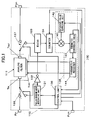
- Fig. 1 is a drawing showing the system configuration of a filter circuit according to an embodiment of the present invention.
- a filter circuit 100 of this embodiment includes an analog filter 111 and a filter adjustment apparatus 112.
- the analog filter 111 receives an input signal supplied to an input terminal Tin, and removes or passes only desired frequency components in the input signal for output from an output terminal Tout.
- the filter adjustment apparatus 112 serves to automatically adjust the characteristics of the analog filter 111.
- the filter adjustment apparatus 112 computes cross-correlation between the output of the analog filter 111 and a pseudo-random pattern to adjust the characteristics of the analog filter based on the computed cross-correlation.
- the filter adjustment apparatus 112 includes a pseudo-random-code generating unit 131, an inverter 132, a logic circuit 133, a counter 134, an adjustment unit 135, switches 136 and 137, and a control unit 138.
- the pseudo-random-code generating unit 131 supplies a pseudo-random code to the input terminal Tin of the analog filter 111.
- the pseudo-random code generated by the pseudo-random-code generating unit 131 may be a Barker sequence code, an M sequence code, a Gold sequence code, a Kasami sequence code, or the like.
- the pseudo-random code generated by the pseudo-random-code generating unit 131 is not limited to these sequence codes, but may be any code as long as it contains various frequency components.
- the pseudo-random code generated by the pseudo-random-code generating unit 131 is supplied to the inverter 132 as well as to the input terminal Tin of the analog filter 111 via the switch 136.
- the inverter 132 inverts the logic of the pseudo-random code generated by the pseudo-random-code generating unit 131 for provision to the logic circuit 133.
- the logic circuit 133 is comprised of an exclusive-OR (EXOR) gate, and produces an exclusive-OR value between the output signal produced at the output terminal Tout of the analog filter 111 and the pseudo-random code generated by the pseudo-random-code generating unit 131.
- EXOR exclusive-OR
- the counter 134 counts the logic output "1" from the logic circuit 133.
- the adjustment unit 135 adjusts the characteristics of the analog filter 111 based on the count obtained by the counter 134.
- the switch 136 is situated between the pseudo-random-code generating unit 131, an input port Pin, and the input terminal Tin of the analog filter 111.
- the switch 136 disconnects the input port Pin as shown by the solid line at the time of adjustment under the control of the control unit 138 to supply the pseudo-random code generated by the pseudo-random-code generating unit 131 to the input terminal Tin of the analog filter 111.
- the switch 136 closes the connection between the input terminal Tin of the analog filter 111 and the pseudo-random-code generating unit 131 as shown by the dotted line at the time of normal operation to connect between the input terminal Tin of the analog filter 111 and the input port Pin.
- the switch 137 is situated between the logic circuit 133, an output port Pout, and the output terminal Tout of the analog filter 111.
- the switch 137 disconnects the output terminal Tout of the analog filter 111 from the output port Pout at the time of adjustment under the control of the control unit 138 to connect the output terminal Tout to the logic circuit 133.
- the switch 137 is controlled to connect the output terminal Tout of the analog filter 111 to the output port Pout at the time of normal operation.
- the control unit 138 controls the operations of the switches 136 and 137 and the adjustment unit 135 in response to an adjustment control signal supplied to a control port Pcnt.
- the adjustment unit 135 includes a subtraction unit 141, a reference-value supplying unit 142, a parameter conversion table 143, and a parameter register 144.
- the subtraction unit 141 subtracts a reference value supplied from the reference-value supplying unit 142 from the count value supplied from the counter 134.
- the outcome of the subtraction obtained by the subtraction unit 141 represents an error from the reference value.
- the output of the subtraction unit 141 is supplied to the parameter conversion table 143 and the control unit 138.
- the parameter conversion table 143 has parameter values stored in advance that are associated with error values deviating from the reference value. Parameter values may be each comprised of a 6-bit bit sequence. The parameter conversion table 143 supplies the parameter value corresponding to the output of the subtraction unit 141 to the parameter register 144.
- the parameter register 144 stores therein the parameter value supplied from the parameter conversion table 143.
- the parameter value stored in the parameter register 144 is supplied in parallel to control input terminals Tcnt of the analog filter 111.
- Fig. 2 is a block diagram of the analog filter 111.
- the analog filter 111 includes first through third active filter circuit units 151 through 153 connected in series, and constitutes a low-pass filter.
- the first active filter circuit unit 151 includes variable capacitance circuits C11 and C12.
- the second active filter circuit unit 152 includes variable capacitance circuits C21 and C22.
- the third active filter circuit unit 153 includes variable capacitance circuits C31 and C32.
- the analog filter 111 is configured such that its frequency characteristics are adjustable by controlling the capacitances of the variable capacitance circuits C11, C12, C21, C22, C31, and C32 in response to control signals supplied to the control input terminals Tcnt.
- Fig. 3 is a drawing showing the circuit configuration of the variable capacitance circuit C11.
- the variable capacitance circuit C11 includes 7 capacitors C110 through C116 and 6 switches 171 through 176, for example.
- the capacitor C111 has a capacitance of 32 pF, for example, and is connected to the switch 171 in series.
- the capacitor C112 has a capacitance of 16 pF, for example, and is connected to the switch 172 in series.
- the capacitor C113 has a capacitance of 8 pF, for example, and is connected to the switch 173 in series.
- the capacitor C114 has a capacitance of 4 pF, for example, and is connected to the switch 174 in series.
- the capacitor C115 has a capacitance of 2 pF, for example, and is connected to the switch 175 in series.
- the capacitor C116 has a capacitance of 1 pF, for example, and is connected to the switch 176 in series.
- the capacitor C110 has a capacitance of 36 pF, for example, and is connected in parallel to the series-connected capacitor C111 and switch 171, the series-connected capacitor C112 and switch 172, the series-connected capacitor C113 and switch 173, the series-connected capacitor C114 and switch 174, the series-connected capacitor C115 and switch 175, and the series-connected capacitor C116 and switch 176.
- the switch 171 receives the value of the first bit among the 6 bits of the parameter value supplied to the control terminal Tcnt.
- the switch 171 becomes ON when the value of the first bit is "1" , and becomes OFF when the value of the first bit is "0".
- the switch 172 receives the value of the second bit among the 6 bits of the parameter value supplied to the control terminal Tcnt.
- the switch 172 becomes ON when the value of the second bit is "1" , and becomes OFF when the value of the second bit is "0" .
- the switch 173 receives the value of the third bit among the 6 bits of the parameter value supplied to the control terminal Tcnt.
- the switch 173 becomes ON when the value of the third bit is "1" , and becomes OFF when the value of the third bit is "0" .
- the switch 174 receives the value of the fourth bit among the 6 bits of the parameter value supplied to the control terminal Tcnt.
- the switch 174 becomes ON when the value of the fourth bit is "1" , and becomes OFF when the value of the fourth bit is "0" .
- the switch 175 receives the value of the fifth bit among the 6 bits of the parameter value supplied to the control terminal Tcnt.
- the switch 175 becomes ON when the value of the fifth bit is "1" , and becomes OFF when the value of the fifth bit is "0".
- the switch 176 receives the value of the sixth bit among the 6 bits of the parameter value supplied to the control terminal Tcnt.
- the switch 176 becomes ON when the value of the sixth bit is "1" , and becomes OFF when the value of the sixth bit is "0".
- the switches 171, 172, 175, and 176 are ON, and the switches 173 and 174 are OFF.
- the capacitance of the variable capacitance circuit C11 is set equal to 87 pF, which is the capacitance obtained by connecting the capacitors C110, C111, C112, C115, and C116 in parallel.
- the switches 171, 173, and 175 are ON, and the switches 172, 174, and 176 are OFF, resulting in the capacitance of the variable capacitance circuit C11 being 42 pF.
- variable capacitance circuits C12, C21, C22, C31, and C32 each have a similar configuration to the variable capacitance circuit C11, so that their capacitances can be changed in response to the parameter value stored in the parameter register 144.
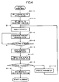
- Fig. 4 is a flowchart showing an adjustment operation performed by the control unit 138.
- Fig. 5 is a drawing showing operating waveforms according to an embodiment of the present invention.
- Fig. 5-(A) shows a Barker sequence code.
- Fig. 5-(B) shows a waveform of the output of the analog filter 111 in response to the Barker sequence code.
- Fig. 5-(C) shows a waveform of the output of the logic circuit 133.
- the control unit 138 controls the parameter conversion table 143 in step S1-1 to set an initial value to the parameter register 144 from the parameter conversion table 143.
- the initial value may be set approximately to a middle value in the range of the variable capacitance of the variable capacitance circuits.
- the range of the variable capacitance of the variable capacitance circuit C11 is from 36 pF to 100 pF, and the middle value in this variable capacitance range is 67 pF.
- the parameter value may thus be set to "101111".
- This parameter value "101111” is set as an initial value for the variable capacitance circuit C11.
- the variable capacitance circuits C12, C21, C22, C31, and C32 each have their initial value set similarly to the manner in which the initial value is set for the variable capacitance circuit C11.
- the control unit 138 switches the switch 136 in step S1-2 to supply the output of the pseudo-random-code generating unit 131 to the input terminal Tin of the analog filter 111, and, also, switches the switch 137 to connect the output terminal Tout of the analog filter 111 to the logic circuit 133.
- the control unit 138 resets the output of the counter 134 to "0" in step S1-3.
- the control unit 138 activates the pseudo-random-code generating unit 131 in step S1-4.
- the pseudo-random-code generating unit 131 generates a pseudo-random code specified by the control unit 138.
- the pseudo-random code generated by the pseudo-random-code generating unit 131 is supplied to the input terminal Tin of the analog filter 111 via the switch 136, and is also supplied to the logic circuit 133 after logic inversion by the inverter 132.
- the input terminal Tin of the analog filter 111 receives a Barker sequence code as shown in Fig. 5-(A) .
- the Barker sequence code passing through the analog filter 111 is output as a waveform as shown in Fig. 5-(B) due to the frequency characteristics set in the analog filter 111.
- the waveform as shown in Fig. 5-(B) output from the analog filter 111 is supplied to the logic circuit 133.
- the logic circuit 133 produces an exclusive-OR value between the signal obtained by inverting the Barker sequence code and the output signal of the analog filter 111.
- the output of the logic circuit 133 assumes "1" and “0” alternating at predetermined sampling frequencies as shown in Fig. 5-(C) .
- the counter 134 counts the output logic value "1" of the logic circuit 133 shown in Fig. 5-(C) .
- the control unit 138 checks in step S1-5 whether pseudo-random codes are generated N times, which is a number specified in advance. Upon finding in step S1-5 that pseudo-random codes have been generated N times, the control unit 138 controls the pseudo-random-code generating unit 131 in step S1-6 to stop the generation of pseudo-random codes.
- the control unit 138 controls the counter 134 and the reference-value supplying unit 142 in step S1-7 to compute an error that is a difference between the count of the counter 134 and the reference value of the reference-value supplying unit 142.
- the control unit 138 determines that the adjustment of the analog filter 111 is not necessary. In this case, the control unit 138 switches the switch 136 to couple the input port Pin to the input terminal Tin of the analog filter 111, and also switches the switch 137 to couple the output terminal Tout of the analog filter 111 to the output port Pout.
- step S1-8 the control unit 138 supplies the error value to the parameter conversion table 143 in step S1-10 to set a 6-bit parameter value corresponding to the error value to the parameter register 144, thereby adjusting the frequency characteristics of the analog filter 111.
- the procedure returns to step S1-3. Subsequently, a check as to the need of the adjustment of frequency characteristics of the analog filter 111 is performed again.
- the setting of a parameter value in the parameter register 144 as described above causes the variable capacitance circuits C11, C12, C21, C22, C31, and C32 of the analog filter 111 to assume capacitance values corresponding to the parameter value set in the parameter register 144. This makes it possible to adjust the frequency characteristics of the analog filter 111.
- the control unit 138 repeats steps S1-3 through S1-8 until the error falls within the tolerable range.
- Fig. 6 is a drawing showing an example of the relationship between the cutoff frequency of the analog filter 111 and the count of the counter 134.
- the count of the counter 134 may be " 319 " for cutoff frequencies of 6.98 MHz and 6.99 MHz, "351” for cutoff frequencies of 7.01 MHz and 7.02 MHz, and "335" for a cutoff frequency of 7.00 MHz.
- the cutoff frequency of the analog filter 111 is to be set to 7.00 MHz
- the reference value supplied from the reference-value supplying unit 142 to the subtraction unit 141 is set to "335" . If the frequency characteristics at present are such that the cutoff frequency is 6.98 MHz or 6.99 MHz, the count becomes 319.
- a negative error causes such a parameter value to be selected that the capacitances of the variable capacitance circuits C11, C12, C21, C22, C31, and C32 are changed to increase the cutoff frequency of the analog filter 111.
- a positive error causes such a parameter value to be selected that the capacitances of the variable capacitance circuits C11, C12, C21, C22, C31, and C32 are changed to decrease the cutoff frequency of the analog filter 111.
- the frequency characteristics of the analog filter 111 can be evaluated without digitizing the output of the analog filter 111, and the parameter of the analog filter 111 can be adjusted based on this evaluation.
- This makes it possible to provide the filter adjustment apparatus 112 having a relatively simple configuration, so that the filter adjustment apparatus 112 can be implemented on the same semiconductor chip that carries the analog filter 111.
- the adjustment of the analog filter 111 can be automatically performed at constant time intervals upon power-on. This makes it possible to attain desired frequency characteristics through automatic adjustment even when parameters are changed with temporal deterioration in the circuit.
- an output obtained by performing logical operation between the output of the analog filter and a pseudo-random code is counted by the counter, the count of which is then used to perform filter adjustment.
- various modifications may be made as it suffices to compute a cross-correlation between the analog filter and a pseudo-random code.
- a CCD charge coupled device
- the like may be employed to compute a cross-correlation between the output of an analog filter and a pseudo-random code.
- an active low-pass filter serves as the analog filter 111.
- the analog filter 111 is not limited to a low-pass filter.
- the present invention is applicable to filters having other frequency characteristics such as a high-pass filter, a band-pass filter, a band-eliminate filter, etc.
- an error is converted by use of the parameter conversion table 143.
- a parameter value may be obtained through computation from an error.
- the present invention is applicable to filter circuits as well as filter adjustment methods and filter adjustment apparatuses for adjusting the characteristics of analog filters.
Landscapes
- Networks Using Active Elements (AREA)
Abstract
The object is to provide a filter circuit as well as a filter adjustment method and a filter adjustment apparatus that can adjust the characteristics of an analog filter by use of a simple configuration.
A filter adjustment method of adjusting the characteristics of an analog filter (111) includes supplying a pseudo-random code to the analog filter (111), computing a cross-correlation between an output of the analog filter (111) and the pseudo-random code, and adjusting the characteristics of the analog filter based on the computed cross-correlation.
Description
- The present invention generally relates to filter circuits as well as filter adjustment methods and filter adjustment apparatuses for adjusting the characteristics of analog filters, and particularly relates to filter circuits as well as filter adjustment methods and filter adjustment apparatuses for adjusting the characteristics of analog filters.
- In electronic apparatuses such as communication equipment, analog filters are often used to allow the passage of signals only in a preferred frequency band. In recent years, there has been a need to implement an analog filter on a semiconductor chip in response to the demand for size reduction of apparatuses.
- Conventional analog filters require adjustment in order to control frequency characteristics attributable to variation in the parameters of device components. It is customary to adjust the frequency characteristics of an analog filter by use of an outside part or the like. When an outside capacitance is used to adjust an analog filter, for example, the chip tends to become large because of the need to provide terminals for coupling to the adjustment-purpose capacitance. In consideration of this, there is a need to implement an automatic adjustment circuit for automatically adjusting the frequency characteristics of an analog filter on the same semiconductor chip that carries the analog filter.
- Conventional automatic adjustment is performed by supplying a reference signal to a filter, comparing phases between the output of the filter and the reference signal, and controlling the transfer function of the filter based on the phase comparison (see
Patent Document 1, for example). - [Patent Document 1] Japanese Patent Application Publication No.
3-114391 - In the conventional filter adjustment methods, the problem is that a phase comparator, a loop filter, a DC amplifier, and so on are all analog circuits, so that variations in these adjustment-purpose circuits affect the frequency characteristics of the filter. The adjustment process may be digitized in order to improve adjustment accuracy. For such digitization, however, an AD converter and a DA converter are required, and, the number of bits needs to be large for the purpose of providing high accuracy. This results in the size of the circuits being large. Such digitization cannot be employed because the provision of the adjustment circuits on the same chip that carries the filter results in a large chip size.
- It is an object of the present invention to provide a filter circuit as well as a filter adjustment method and a filter adjustment apparatus that can perform automatic adjustment by use of a simple configuration.
- According to a characteristic aspect of the invention, a filter adjustment method of adjusting characteristics of an analog filter includes: supplying a pseudo-random code to the analog filter; computing a cross-correlation between an output of the analog filter and the pseudo-random code; and adjusting characteristics of the analog filter based on the cross-correlation.
- The cross-correlation may be an exclusive-OR value between the output of the analog filter and the pseudo-random code.
- According to another characteristic aspect of the invention, a filter adjustment apparatus for adjusting characteristics of an analog filter includes: a pseudo-random-code generating unit to supply a pseudo-random code to the analog filter; a cross-correlation computing circuit to compute a cross-correlation between an output of the analog filter and the pseudo-random code generated by the pseudo-random-code generating unit; and an adjustment unit to adjust characteristics of the analog filter based on the cross-correlation.
- The cross-correlation computing circuit may include a logic circuit to perform a logical operation between the output of the analog filter and the pseudo-random code generated by the pseudo-random-code generating unit, and may include a counter to count an output of the logic circuit, wherein the adjustment unit may adjust the characteristics of the analog filter based on the count obtained by the counter.
- The logic circuit may perform an exclusive-OR operation between the output of the analog filter and the pseudo-random code.
- According to another characteristic aspect of the invention, a filter circuit includes: an analog filter to receive an input signal supplied to an input terminal and to output from an output terminal an output signal obtained by removing or passing desired frequency components in the input signal; a pseudo-random-code generating unit to supply a pseudo-random code to the input terminal of the analog filter; a cross-correlation computing circuit to compute a cross-correlation between an output signal output from the output terminal of the analog filter and the pseudo-random code; and an adjustment unit to adjust characteristics of the analog filter based on the cross-correlation.
- The cross-correlation computing circuit may include a logic circuit to perform a logical operation between the output of the analog filter and the pseudo-random code generated by the pseudo-random-code generating unit, and may include a counter to produce a count obtained by counting an output of the logic circuit, wherein the adjustment unit may adjust the characteristics of the analog filter based on the count obtained by the counter.
- The logic circuit may perform an exclusive-OR operation between the output of the analog filter and the pseudo-random code.
- According to an embodiment of the present invention, a cross-correlation between the output of the analog filter and the pseudo-random pattern is computed, and the characteristics of the analog filter are adjusted based on the computed cross-correlation. This makes it possible to evaluate and adjust the characteristics of the analog filter without digitizing the output of the analog filter. Accordingly, the adjustment circuit and the analog filter can be implemented on the same semiconductor chip.
-
-
Fig. 1 is a drawing showing the system configuration of a filter circuit according to an embodiment of the present invention. -
Fig. 2 is a block diagram of theanalog filter 111 shown inFig. 1 . -
Fig. 3 is a drawing showing the circuit configuration of the variable capacitance circuit C11 shown inFig. 2 . -
Fig. 4 is a flowchart showing the procedure of an adjustment operation performed by thecontrol unit 138 shown inFig. 1 . -
Fig. 5 is a drawing showing the operating waveforms of a filter circuit according to an embodiment of the present invention. -
Fig. 6 is a drawing showing an example of the relationship between the cutoff frequency of theanalog filter 111 and the count of thecounter 134. -
- 100
- filter circuit
- 111
- analog filter
- 112
- filter adjustment apparatus
- 131
- pseudo-random-code generating unit
- 132
- inverter
- 133
- logic circuit
- 134
- counter
- 135
- adjustment unit
- 136, 137
- switch
- 138
- control unit
- 141
- subtraction unit
- 142
- reference-value supplying unit
- 143
- parameter conversion table
- 144
- parameter register
-
Fig. 1 is a drawing showing the system configuration of a filter circuit according to an embodiment of the present invention. - A
filter circuit 100 of this embodiment includes ananalog filter 111 and afilter adjustment apparatus 112. - The
analog filter 111 receives an input signal supplied to an input terminal Tin, and removes or passes only desired frequency components in the input signal for output from an output terminal Tout. - The
filter adjustment apparatus 112 serves to automatically adjust the characteristics of theanalog filter 111. Thefilter adjustment apparatus 112 computes cross-correlation between the output of theanalog filter 111 and a pseudo-random pattern to adjust the characteristics of the analog filter based on the computed cross-correlation. Thefilter adjustment apparatus 112 includes a pseudo-random-code generating unit 131, aninverter 132, alogic circuit 133, acounter 134, anadjustment unit 135,switches control unit 138. - The pseudo-random-
code generating unit 131 supplies a pseudo-random code to the input terminal Tin of theanalog filter 111. The pseudo-random code generated by the pseudo-random-code generating unit 131 may be a Barker sequence code, an M sequence code, a Gold sequence code, a Kasami sequence code, or the like. The pseudo-random code generated by the pseudo-random-code generating unit 131 is not limited to these sequence codes, but may be any code as long as it contains various frequency components. - The pseudo-random code generated by the pseudo-random-
code generating unit 131 is supplied to theinverter 132 as well as to the input terminal Tin of theanalog filter 111 via theswitch 136. Theinverter 132 inverts the logic of the pseudo-random code generated by the pseudo-random-code generating unit 131 for provision to thelogic circuit 133. - The
logic circuit 133 is comprised of an exclusive-OR (EXOR) gate, and produces an exclusive-OR value between the output signal produced at the output terminal Tout of theanalog filter 111 and the pseudo-random code generated by the pseudo-random-code generating unit 131. - The
counter 134 counts the logic output "1" from thelogic circuit 133. Theadjustment unit 135 adjusts the characteristics of theanalog filter 111 based on the count obtained by thecounter 134. - The
switch 136 is situated between the pseudo-random-code generating unit 131, an input port Pin, and the input terminal Tin of theanalog filter 111. Theswitch 136 disconnects the input port Pin as shown by the solid line at the time of adjustment under the control of thecontrol unit 138 to supply the pseudo-random code generated by the pseudo-random-code generating unit 131 to the input terminal Tin of theanalog filter 111. Theswitch 136 closes the connection between the input terminal Tin of theanalog filter 111 and the pseudo-random-code generating unit 131 as shown by the dotted line at the time of normal operation to connect between the input terminal Tin of theanalog filter 111 and the input port Pin. - The
switch 137 is situated between thelogic circuit 133, an output port Pout, and the output terminal Tout of theanalog filter 111. Theswitch 137 disconnects the output terminal Tout of theanalog filter 111 from the output port Pout at the time of adjustment under the control of thecontrol unit 138 to connect the output terminal Tout to thelogic circuit 133. Theswitch 137 is controlled to connect the output terminal Tout of theanalog filter 111 to the output port Pout at the time of normal operation. - The
control unit 138 controls the operations of theswitches adjustment unit 135 in response to an adjustment control signal supplied to a control port Pcnt. - The
adjustment unit 135 includes asubtraction unit 141, a reference-value supplying unit 142, a parameter conversion table 143, and aparameter register 144. - The
subtraction unit 141 subtracts a reference value supplied from the reference-value supplying unit 142 from the count value supplied from thecounter 134. The outcome of the subtraction obtained by thesubtraction unit 141 represents an error from the reference value. The output of thesubtraction unit 141 is supplied to the parameter conversion table 143 and thecontrol unit 138. - The parameter conversion table 143 has parameter values stored in advance that are associated with error values deviating from the reference value. Parameter values may be each comprised of a 6-bit bit sequence. The parameter conversion table 143 supplies the parameter value corresponding to the output of the
subtraction unit 141 to theparameter register 144. - The
parameter register 144 stores therein the parameter value supplied from the parameter conversion table 143. The parameter value stored in theparameter register 144 is supplied in parallel to control input terminals Tcnt of theanalog filter 111. -
Fig. 2 is a block diagram of theanalog filter 111. - The
analog filter 111 includes first through third activefilter circuit units 151 through 153 connected in series, and constitutes a low-pass filter. The first activefilter circuit unit 151 includes variable capacitance circuits C11 and C12. The second activefilter circuit unit 152 includes variable capacitance circuits C21 and C22. The third activefilter circuit unit 153 includes variable capacitance circuits C31 and C32. - The
analog filter 111 is configured such that its frequency characteristics are adjustable by controlling the capacitances of the variable capacitance circuits C11, C12, C21, C22, C31, and C32 in response to control signals supplied to the control input terminals Tcnt. -
Fig. 3 is a drawing showing the circuit configuration of the variable capacitance circuit C11. - The variable capacitance circuit C11 includes 7 capacitors C110 through C116 and 6
switches 171 through 176, for example. - The capacitor C111 has a capacitance of 32 pF, for example, and is connected to the
switch 171 in series. The capacitor C112 has a capacitance of 16 pF, for example, and is connected to theswitch 172 in series. The capacitor C113 has a capacitance of 8 pF, for example, and is connected to theswitch 173 in series. The capacitor C114 has a capacitance of 4 pF, for example, and is connected to theswitch 174 in series. The capacitor C115 has a capacitance of 2 pF, for example, and is connected to theswitch 175 in series. The capacitor C116 has a capacitance of 1 pF, for example, and is connected to theswitch 176 in series. - The capacitor C110 has a capacitance of 36 pF, for example, and is connected in parallel to the series-connected capacitor C111 and switch 171, the series-connected capacitor C112 and switch 172, the series-connected capacitor C113 and switch 173, the series-connected capacitor C114 and switch 174, the series-connected capacitor C115 and switch 175, and the series-connected capacitor C116 and
switch 176. - The
switch 171 receives the value of the first bit among the 6 bits of the parameter value supplied to the control terminal Tcnt. Theswitch 171 becomes ON when the value of the first bit is "1" , and becomes OFF when the value of the first bit is "0". - The
switch 172 receives the value of the second bit among the 6 bits of the parameter value supplied to the control terminal Tcnt. Theswitch 172 becomes ON when the value of the second bit is "1" , and becomes OFF when the value of the second bit is "0" . - The
switch 173 receives the value of the third bit among the 6 bits of the parameter value supplied to the control terminal Tcnt. Theswitch 173 becomes ON when the value of the third bit is "1" , and becomes OFF when the value of the third bit is "0" . - The
switch 174 receives the value of the fourth bit among the 6 bits of the parameter value supplied to the control terminal Tcnt. Theswitch 174 becomes ON when the value of the fourth bit is "1" , and becomes OFF when the value of the fourth bit is "0" . - The
switch 175 receives the value of the fifth bit among the 6 bits of the parameter value supplied to the control terminal Tcnt. Theswitch 175 becomes ON when the value of the fifth bit is "1" , and becomes OFF when the value of the fifth bit is "0". - The
switch 176 receives the value of the sixth bit among the 6 bits of the parameter value supplied to the control terminal Tcnt. Theswitch 176 becomes ON when the value of the sixth bit is "1" , and becomes OFF when the value of the sixth bit is "0". - When the parameter value is "110011" , for example, the
switches switches switches switches - In this manner, the use of the parameter value stored in the
parameter register 144 can change the capacitance of the capacitor C11. The variable capacitance circuits C12, C21, C22, C31, and C32 each have a similar configuration to the variable capacitance circuit C11, so that their capacitances can be changed in response to the parameter value stored in theparameter register 144. - In the following, an adjustment operation will be described.
-
Fig. 4 is a flowchart showing an adjustment operation performed by thecontrol unit 138.Fig. 5 is a drawing showing operating waveforms according to an embodiment of the present invention.Fig. 5-(A) shows a Barker sequence code.Fig. 5-(B) shows a waveform of the output of theanalog filter 111 in response to the Barker sequence code.Fig. 5-(C) shows a waveform of the output of thelogic circuit 133. - The
control unit 138 controls the parameter conversion table 143 in step S1-1 to set an initial value to theparameter register 144 from the parameter conversion table 143. The initial value may be set approximately to a middle value in the range of the variable capacitance of the variable capacitance circuits. To be specific, the range of the variable capacitance of the variable capacitance circuit C11 is from 36 pF to 100 pF, and the middle value in this variable capacitance range is 67 pF. The parameter value may thus be set to "101111". This parameter value "101111" is set as an initial value for the variable capacitance circuit C11. The variable capacitance circuits C12, C21, C22, C31, and C32 each have their initial value set similarly to the manner in which the initial value is set for the variable capacitance circuit C11. - The
control unit 138 switches theswitch 136 in step S1-2 to supply the output of the pseudo-random-code generating unit 131 to the input terminal Tin of theanalog filter 111, and, also, switches theswitch 137 to connect the output terminal Tout of theanalog filter 111 to thelogic circuit 133. Thecontrol unit 138 resets the output of thecounter 134 to "0" in step S1-3. - The
control unit 138 activates the pseudo-random-code generating unit 131 in step S1-4. The pseudo-random-code generating unit 131 generates a pseudo-random code specified by thecontrol unit 138. The pseudo-random code generated by the pseudo-random-code generating unit 131 is supplied to the input terminal Tin of theanalog filter 111 via theswitch 136, and is also supplied to thelogic circuit 133 after logic inversion by theinverter 132. The input terminal Tin of theanalog filter 111 receives a Barker sequence code as shown inFig. 5-(A) . - The Barker sequence code passing through the
analog filter 111 is output as a waveform as shown inFig. 5-(B) due to the frequency characteristics set in theanalog filter 111. - The waveform as shown in
Fig. 5-(B) output from theanalog filter 111 is supplied to thelogic circuit 133. Thelogic circuit 133 produces an exclusive-OR value between the signal obtained by inverting the Barker sequence code and the output signal of theanalog filter 111. The output of thelogic circuit 133 assumes "1" and "0" alternating at predetermined sampling frequencies as shown inFig. 5-(C) . Thecounter 134 counts the output logic value "1" of thelogic circuit 133 shown inFig. 5-(C) . - The
control unit 138 checks in step S1-5 whether pseudo-random codes are generated N times, which is a number specified in advance. Upon finding in step S1-5 that pseudo-random codes have been generated N times, thecontrol unit 138 controls the pseudo-random-code generating unit 131 in step S1-6 to stop the generation of pseudo-random codes. - The
control unit 138 controls thecounter 134 and the reference-value supplying unit 142 in step S1-7 to compute an error that is a difference between the count of thecounter 134 and the reference value of the reference-value supplying unit 142. Upon finding in step S1-8 that the error is within a tolerable range, thecontrol unit 138 determines that the adjustment of theanalog filter 111 is not necessary. In this case, thecontrol unit 138 switches theswitch 136 to couple the input port Pin to the input terminal Tin of theanalog filter 111, and also switches theswitch 137 to couple the output terminal Tout of theanalog filter 111 to the output port Pout. - Further, upon finding in step S1-8 that the error is outside the tolerable range, the
control unit 138 supplies the error value to the parameter conversion table 143 in step S1-10 to set a 6-bit parameter value corresponding to the error value to theparameter register 144, thereby adjusting the frequency characteristics of theanalog filter 111. After this adjustment, the procedure returns to step S1-3. Subsequently, a check as to the need of the adjustment of frequency characteristics of theanalog filter 111 is performed again. - The setting of a parameter value in the
parameter register 144 as described above causes the variable capacitance circuits C11, C12, C21, C22, C31, and C32 of theanalog filter 111 to assume capacitance values corresponding to the parameter value set in theparameter register 144. This makes it possible to adjust the frequency characteristics of theanalog filter 111. - The
control unit 138 repeats steps S1-3 through S1-8 until the error falls within the tolerable range. -
Fig. 6 is a drawing showing an example of the relationship between the cutoff frequency of theanalog filter 111 and the count of thecounter 134. - As shown in
Fig. 6 , for example, the count of thecounter 134 may be " 319 " for cutoff frequencies of 6.98 MHz and 6.99 MHz, "351" for cutoff frequencies of 7.01 MHz and 7.02 MHz, and "335" for a cutoff frequency of 7.00 MHz. - In this case, if the cutoff frequency of the
analog filter 111 is to be set to 7.00 MHz, the reference value supplied from the reference-value supplying unit 142 to thesubtraction unit 141 is set to "335" . If the frequency characteristics at present are such that the cutoff frequency is 6.98 MHz or 6.99 MHz, the count becomes 319. The error output from thesubtraction unit 141 is -14 (=319-335) in this case. If the frequency characteristics at any given time are such that the cutoff frequency is 7.01 MHz or 7.02 MHz, the count becomes 351. The error output from thesubtraction unit 141 is 16 (=351-335) in this case. - A negative error causes such a parameter value to be selected that the capacitances of the variable capacitance circuits C11, C12, C21, C22, C31, and C32 are changed to increase the cutoff frequency of the
analog filter 111. A positive error causes such a parameter value to be selected that the capacitances of the variable capacitance circuits C11, C12, C21, C22, C31, and C32 are changed to decrease the cutoff frequency of theanalog filter 111. - According to the embodiment, the frequency characteristics of the
analog filter 111 can be evaluated without digitizing the output of theanalog filter 111, and the parameter of theanalog filter 111 can be adjusted based on this evaluation. This makes it possible to provide thefilter adjustment apparatus 112 having a relatively simple configuration, so that thefilter adjustment apparatus 112 can be implemented on the same semiconductor chip that carries theanalog filter 111. - Further, with this configuration in which the
analog filter 111 and thefilter adjustment apparatus 112 are implemented on the same semiconductor chip, the adjustment of theanalog filter 111 can be automatically performed at constant time intervals upon power-on. This makes it possible to attain desired frequency characteristics through automatic adjustment even when parameters are changed with temporal deterioration in the circuit. - In the present embodiment, an output obtained by performing logical operation between the output of the analog filter and a pseudo-random code is counted by the counter, the count of which is then used to perform filter adjustment. Needless to say, however, various modifications may be made as it suffices to compute a cross-correlation between the analog filter and a pseudo-random code. For example, a CCD (charge coupled device) or the like may be employed to compute a cross-correlation between the output of an analog filter and a pseudo-random code.
- In the present embodiment, further, a description has been given with reference to an example in which an active low-pass filter serves as the
analog filter 111. Notwithstanding this, theanalog filter 111 is not limited to a low-pass filter. The present invention is applicable to filters having other frequency characteristics such as a high-pass filter, a band-pass filter, a band-eliminate filter, etc. - In the present embodiment, moreover, an error is converted by use of the parameter conversion table 143. Alternatively, a parameter value may be obtained through computation from an error.
- The present invention is applicable to filter circuits as well as filter adjustment methods and filter adjustment apparatuses for adjusting the characteristics of analog filters.
- This international application claims foreign priority to Japanese Patent Application No.
2005-333084 filed on November 17, 2005
Claims (8)
- A filter adjustment method of adjusting characteristics of an analog filter, comprising:supplying a pseudo-random code to the analog filter;computing a cross-correlation between an output of the analog filter and the pseudo-random code; andadjusting characteristics of the analog filter based on the cross-correlation.
- The filter adjustment method as claimed in claim 1, wherein the cross-correlation is an exclusive-OR value between the output of the analog filter and the pseudo-random code.
- A filter adjustment apparatus for adjusting characteristics of an analog filter, comprising:a pseudo-random-code generating unit to supply a pseudo-random code to the analog filter;a cross-correlation computing circuit to compute a cross-correlation between an output of the analog filter and the pseudo-random code generated by the pseudo-random-code generating unit; andan adjustment unit to adjust characteristics of the analog filter based on the cross-correlation.
- The filter adjustment apparatus as claimed in claim 3, wherein the cross-correlation computing circuit includes:a logic circuit to perform a logical operation between the output of the analog filter and the pseudo-random code generated by the pseudo-random-code generating unit; anda counter to count an output of the logic circuit,wherein the adjustment unit adjusts the characteristics of the analog filter based on the count obtained by the counter.
- The filter adjustment apparatus as claimed in claim 4, wherein the logic circuit performs an exclusive-OR operation between the output of the analog filter and the pseudo-random code.
- A filter circuit, comprising:an analog filter to receive an input signal supplied to an input terminal and to output from an output terminal an output signal obtained by removing or passing desired frequency components in the input signal;a pseudo-random-code generating unit to supply a pseudo-random code to the input terminal of the analog filter;a cross-correlation computing circuit to compute a cross-correlation between an output signal output from the output terminal of the analog filter and the pseudo-random code; andan adjustment unit to adjust characteristics of the analog filter based on the cross-correlation.
- The filter circuit as claimed in claim 6, wherein the cross-correlation computing circuit includes:a logic circuit to perform a logical operation between the output of the analog filter and the pseudo-random code generated by the pseudo-random-code generating unit; anda counter to produce a count obtained by counting an output of the logic circuit,wherein the adjustment unit adjusts the characteristics of the analog filter based on the count obtained by the counter.
- The filter circuit as claimed in claim 7, wherein the logic circuit performs an exclusive-OR operation between the output of the analog filter and the pseudo-random code.
Applications Claiming Priority (2)
| Application Number | Priority Date | Filing Date | Title |
|---|---|---|---|
| JP2005333084A JP2007142755A (en) | 2005-11-17 | 2005-11-17 | Filter adjustment method, filter adjustment device, and filter circuit |
| PCT/JP2006/317266 WO2007058012A1 (en) | 2005-11-17 | 2006-08-31 | Filter adjusting method, filter adjusting device, and filter circuit |
Publications (2)
| Publication Number | Publication Date |
|---|---|
| EP1950884A1 true EP1950884A1 (en) | 2008-07-30 |
| EP1950884A4 EP1950884A4 (en) | 2009-07-29 |
Family
ID=38048404
Family Applications (1)
| Application Number | Title | Priority Date | Filing Date |
|---|---|---|---|
| EP06797226A Withdrawn EP1950884A4 (en) | 2005-11-17 | 2006-08-31 | Filter adjusting method, filter adjusting device, and filter circuit |
Country Status (4)
| Country | Link |
|---|---|
| US (1) | US20090096515A1 (en) |
| EP (1) | EP1950884A4 (en) |
| JP (1) | JP2007142755A (en) |
| WO (1) | WO2007058012A1 (en) |
Families Citing this family (5)
| Publication number | Priority date | Publication date | Assignee | Title |
|---|---|---|---|---|
| JP2011114622A (en) * | 2009-11-27 | 2011-06-09 | Panasonic Corp | Filter automatic adjustment circuit and method, and radio communication equipment |
| JP5423875B2 (en) | 2010-03-23 | 2014-02-19 | 富士通株式会社 | Variable frequency filter |
| JP5517808B2 (en) * | 2010-07-22 | 2014-06-11 | 三菱電機株式会社 | Filter device |
| JP6310222B2 (en) * | 2013-10-04 | 2018-04-11 | 日本電信電話株式会社 | Filter |
| US10270428B1 (en) * | 2018-01-22 | 2019-04-23 | Allegro Microsystems, Llc | Filter circuit with dynamic parameter generation |
Family Cites Families (7)
| Publication number | Priority date | Publication date | Assignee | Title |
|---|---|---|---|---|
| JPH03114391A (en) * | 1989-09-28 | 1991-05-15 | Toshiba Corp | Filter automatic adjustment circuit |
| JPH0983294A (en) * | 1995-09-14 | 1997-03-28 | Asahi Kasei Micro Syst Kk | Gm-c filter circuit and gm-c filter adjusting method |
| US6201835B1 (en) * | 1999-03-05 | 2001-03-13 | Burr-Brown Corporation | Frequency-shaped pseudo-random chopper stabilization circuit and method for delta-sigma modulator |
| JP2002359543A (en) * | 2001-06-01 | 2002-12-13 | Matsushita Electric Ind Co Ltd | Filter circuit and mobile communication device using the same |
| US20030067962A1 (en) * | 2001-10-10 | 2003-04-10 | Daniel Yellin | Determining cross-correlation between spreading sequences |
| US6825713B2 (en) * | 2001-12-11 | 2004-11-30 | International Business Machines Corporation | System and method for bandwidth estimation of an integrated filter |
| US6965275B2 (en) * | 2004-02-13 | 2005-11-15 | Infineon Technologies Ag | Method and apparatus for tuning a filter |
-
2005
- 2005-11-17 JP JP2005333084A patent/JP2007142755A/en active Pending
-
2006
- 2006-08-31 WO PCT/JP2006/317266 patent/WO2007058012A1/en not_active Ceased
- 2006-08-31 US US12/093,386 patent/US20090096515A1/en not_active Abandoned
- 2006-08-31 EP EP06797226A patent/EP1950884A4/en not_active Withdrawn
Also Published As
| Publication number | Publication date |
|---|---|
| JP2007142755A (en) | 2007-06-07 |
| US20090096515A1 (en) | 2009-04-16 |
| EP1950884A4 (en) | 2009-07-29 |
| WO2007058012A1 (en) | 2007-05-24 |
Similar Documents
| Publication | Publication Date | Title |
|---|---|---|
| US7737730B2 (en) | Method of detecting the frequency of an input clock signal of an integrated circuit and integrated circuit | |
| KR20120065369A (en) | Sensor device | |
| CN108270443B (en) | Frequency management for interference reduction of a/D converters powered by switching power converters | |
| TWI678068B (en) | Radio frequency signal amplification device and front-end module | |
| CN110829839A (en) | Power supply control device and control apparatus | |
| US20050168294A1 (en) | Highly stable integrated time reference | |
| US20090096515A1 (en) | Filter adjustment method and filter adjustment apparatus as well as filter circuit | |
| US7675356B2 (en) | Digital controlled filter system and filtering method | |
| JPH0837564A (en) | Device for generating accounting signal in communication system | |
| US20010045864A1 (en) | Method and arrangement for calibrating an active filter | |
| CN112213620B (en) | Harmonic distortion test circuit of communication device | |
| CN105379117B (en) | Systems for generating analog signals | |
| CN113726332A (en) | Phase-locked loop circuit reference spurious elimination method, phase-locked loop circuit reference spurious elimination device and phase-locked loop system | |
| CN100559711C (en) | Method and device for adjusting active filter | |
| CN112114264B (en) | Battery electric quantity detection system | |
| KR20220095708A (en) | All Digital Optical Signal Detection Circuit Using a Counter Inside a Clock Data Recovery IC | |
| US6122495A (en) | Device and method for digitizing a receiver signal strength indicator (RSSI) signal | |
| US12524203B2 (en) | Adding circuit for multi-channel signals and implementation method of adding circuit for multi-channel signals | |
| US6894580B2 (en) | Filter tuner system and method | |
| EP2278715A1 (en) | Inexpensively improving resolution and reducing noise of low-noise signals | |
| CN216561575U (en) | Current transducer circuit | |
| US20020177430A1 (en) | Circuit configuration for metering pulse recognition | |
| US7049987B2 (en) | Arrangement for generating a clock signal for a sigma-delta analog-to-digital converter | |
| US9341661B2 (en) | Tone detector | |
| US20080150626A1 (en) | Time variant filter with reduced settling time |
Legal Events
| Date | Code | Title | Description |
|---|---|---|---|
| PUAI | Public reference made under article 153(3) epc to a published international application that has entered the european phase |
Free format text: ORIGINAL CODE: 0009012 |
|
| 17P | Request for examination filed |
Effective date: 20080506 |
|
| AK | Designated contracting states |
Kind code of ref document: A1 Designated state(s): DE FR GB |
|
| DAX | Request for extension of the european patent (deleted) | ||
| RBV | Designated contracting states (corrected) |
Designated state(s): DE FR GB |
|
| A4 | Supplementary search report drawn up and despatched |
Effective date: 20090629 |
|
| RIC1 | Information provided on ipc code assigned before grant |
Ipc: H03H 11/12 20060101AFI20090623BHEP |
|
| STAA | Information on the status of an ep patent application or granted ep patent |
Free format text: STATUS: THE APPLICATION IS DEEMED TO BE WITHDRAWN |
|
| 18D | Application deemed to be withdrawn |
Effective date: 20100114 |