EP1947918A2 - Electronic device and method of manufacturing same - Google Patents
Electronic device and method of manufacturing same Download PDFInfo
- Publication number
- EP1947918A2 EP1947918A2 EP07121152A EP07121152A EP1947918A2 EP 1947918 A2 EP1947918 A2 EP 1947918A2 EP 07121152 A EP07121152 A EP 07121152A EP 07121152 A EP07121152 A EP 07121152A EP 1947918 A2 EP1947918 A2 EP 1947918A2
- Authority
- EP
- European Patent Office
- Prior art keywords
- film
- substrate
- conductor pattern
- electronic device
- circuit chip
- Prior art date
- Legal status (The legal status is an assumption and is not a legal conclusion. Google has not performed a legal analysis and makes no representation as to the accuracy of the status listed.)
- Granted
Links
Images



Classifications
-
- H—ELECTRICITY
- H05—ELECTRIC TECHNIQUES NOT OTHERWISE PROVIDED FOR
- H05K—PRINTED CIRCUITS; CASINGS OR CONSTRUCTIONAL DETAILS OF ELECTRIC APPARATUS; MANUFACTURE OF ASSEMBLAGES OF ELECTRICAL COMPONENTS
- H05K3/00—Apparatus or processes for manufacturing printed circuits
- H05K3/30—Assembling printed circuits with electric components, e.g. with resistors
-
- H—ELECTRICITY
- H05—ELECTRIC TECHNIQUES NOT OTHERWISE PROVIDED FOR
- H05K—PRINTED CIRCUITS; CASINGS OR CONSTRUCTIONAL DETAILS OF ELECTRIC APPARATUS; MANUFACTURE OF ASSEMBLAGES OF ELECTRICAL COMPONENTS
- H05K3/00—Apparatus or processes for manufacturing printed circuits
- H05K3/30—Assembling printed circuits with electric components, e.g. with resistors
- H05K3/32—Assembling printed circuits with electric components, e.g. with resistors electrically connecting electric components or wires to printed circuits
- H05K3/34—Assembling printed circuits with electric components, e.g. with resistors electrically connecting electric components or wires to printed circuits by soldering
- H05K3/3494—Heating processes for reflow soldering
-
- H—ELECTRICITY
- H05—ELECTRIC TECHNIQUES NOT OTHERWISE PROVIDED FOR
- H05K—PRINTED CIRCUITS; CASINGS OR CONSTRUCTIONAL DETAILS OF ELECTRIC APPARATUS; MANUFACTURE OF ASSEMBLAGES OF ELECTRICAL COMPONENTS
- H05K13/00—Apparatus or processes specially adapted for manufacturing or adjusting assemblages of electric components
- H05K13/04—Mounting of components, e.g. of leadless components
-
- H—ELECTRICITY
- H10—SEMICONDUCTOR DEVICES; ELECTRIC SOLID-STATE DEVICES NOT OTHERWISE PROVIDED FOR
- H10W—GENERIC PACKAGES, INTERCONNECTIONS, CONNECTORS OR OTHER CONSTRUCTIONAL DETAILS OF DEVICES COVERED BY CLASS H10
- H10W72/00—Interconnections or connectors in packages
- H10W72/071—Connecting or disconnecting
- H10W72/072—Connecting or disconnecting of bump connectors
-
- H—ELECTRICITY
- H10—SEMICONDUCTOR DEVICES; ELECTRIC SOLID-STATE DEVICES NOT OTHERWISE PROVIDED FOR
- H10W—GENERIC PACKAGES, INTERCONNECTIONS, CONNECTORS OR OTHER CONSTRUCTIONAL DETAILS OF DEVICES COVERED BY CLASS H10
- H10W74/00—Encapsulations, e.g. protective coatings
- H10W74/01—Manufacture or treatment
- H10W74/012—Manufacture or treatment of encapsulations on active surfaces of flip-chip devices, e.g. forming underfills
-
- H—ELECTRICITY
- H10—SEMICONDUCTOR DEVICES; ELECTRIC SOLID-STATE DEVICES NOT OTHERWISE PROVIDED FOR
- H10W—GENERIC PACKAGES, INTERCONNECTIONS, CONNECTORS OR OTHER CONSTRUCTIONAL DETAILS OF DEVICES COVERED BY CLASS H10
- H10W74/00—Encapsulations, e.g. protective coatings
- H10W74/10—Encapsulations, e.g. protective coatings characterised by their shape or disposition
- H10W74/15—Encapsulations, e.g. protective coatings characterised by their shape or disposition on active surfaces of flip-chip devices, e.g. underfills
-
- H—ELECTRICITY
- H05—ELECTRIC TECHNIQUES NOT OTHERWISE PROVIDED FOR
- H05K—PRINTED CIRCUITS; CASINGS OR CONSTRUCTIONAL DETAILS OF ELECTRIC APPARATUS; MANUFACTURE OF ASSEMBLAGES OF ELECTRICAL COMPONENTS
- H05K1/00—Printed circuits
- H05K1/18—Printed circuits structurally associated with non-printed electric components
- H05K1/189—Printed circuits structurally associated with non-printed electric components characterised by the use of flexible or folded printed circuits
-
- H—ELECTRICITY
- H05—ELECTRIC TECHNIQUES NOT OTHERWISE PROVIDED FOR
- H05K—PRINTED CIRCUITS; CASINGS OR CONSTRUCTIONAL DETAILS OF ELECTRIC APPARATUS; MANUFACTURE OF ASSEMBLAGES OF ELECTRICAL COMPONENTS
- H05K2201/00—Indexing scheme relating to printed circuits covered by H05K1/00
- H05K2201/10—Details of components or other objects attached to or integrated in a printed circuit board
- H05K2201/10613—Details of electrical connections of non-printed components, e.g. special leads
- H05K2201/10621—Components characterised by their electrical contacts
- H05K2201/10674—Flip chip
-
- H—ELECTRICITY
- H05—ELECTRIC TECHNIQUES NOT OTHERWISE PROVIDED FOR
- H05K—PRINTED CIRCUITS; CASINGS OR CONSTRUCTIONAL DETAILS OF ELECTRIC APPARATUS; MANUFACTURE OF ASSEMBLAGES OF ELECTRICAL COMPONENTS
- H05K2201/00—Indexing scheme relating to printed circuits covered by H05K1/00
- H05K2201/10—Details of components or other objects attached to or integrated in a printed circuit board
- H05K2201/10613—Details of electrical connections of non-printed components, e.g. special leads
- H05K2201/10954—Other details of electrical connections
- H05K2201/10977—Encapsulated connections
-
- H—ELECTRICITY
- H05—ELECTRIC TECHNIQUES NOT OTHERWISE PROVIDED FOR
- H05K—PRINTED CIRCUITS; CASINGS OR CONSTRUCTIONAL DETAILS OF ELECTRIC APPARATUS; MANUFACTURE OF ASSEMBLAGES OF ELECTRICAL COMPONENTS
- H05K2203/00—Indexing scheme relating to apparatus or processes for manufacturing printed circuits covered by H05K3/00
- H05K2203/01—Tools for processing; Objects used during processing
- H05K2203/0195—Tool for a process not provided for in H05K3/00, e.g. tool for handling objects using suction, for deforming objects, for applying local pressure
-
- H—ELECTRICITY
- H05—ELECTRIC TECHNIQUES NOT OTHERWISE PROVIDED FOR
- H05K—PRINTED CIRCUITS; CASINGS OR CONSTRUCTIONAL DETAILS OF ELECTRIC APPARATUS; MANUFACTURE OF ASSEMBLAGES OF ELECTRICAL COMPONENTS
- H05K2203/00—Indexing scheme relating to apparatus or processes for manufacturing printed circuits covered by H05K3/00
- H05K2203/02—Details related to mechanical or acoustic processing, e.g. drilling, punching, cutting, using ultrasound
- H05K2203/0278—Flat pressure, e.g. for connecting terminals with anisotropic conductive adhesive
-
- H—ELECTRICITY
- H05—ELECTRIC TECHNIQUES NOT OTHERWISE PROVIDED FOR
- H05K—PRINTED CIRCUITS; CASINGS OR CONSTRUCTIONAL DETAILS OF ELECTRIC APPARATUS; MANUFACTURE OF ASSEMBLAGES OF ELECTRICAL COMPONENTS
- H05K3/00—Apparatus or processes for manufacturing printed circuits
- H05K3/30—Assembling printed circuits with electric components, e.g. with resistors
- H05K3/303—Assembling printed circuits with electric components, e.g. with resistors with surface mounted components
- H05K3/305—Affixing by adhesive
-
- H—ELECTRICITY
- H05—ELECTRIC TECHNIQUES NOT OTHERWISE PROVIDED FOR
- H05K—PRINTED CIRCUITS; CASINGS OR CONSTRUCTIONAL DETAILS OF ELECTRIC APPARATUS; MANUFACTURE OF ASSEMBLAGES OF ELECTRICAL COMPONENTS
- H05K3/00—Apparatus or processes for manufacturing printed circuits
- H05K3/38—Improvement of the adhesion between the insulating substrate and the metal
- H05K3/381—Improvement of the adhesion between the insulating substrate and the metal by special treatment of the substrate
-
- H—ELECTRICITY
- H10—SEMICONDUCTOR DEVICES; ELECTRIC SOLID-STATE DEVICES NOT OTHERWISE PROVIDED FOR
- H10W—GENERIC PACKAGES, INTERCONNECTIONS, CONNECTORS OR OTHER CONSTRUCTIONAL DETAILS OF DEVICES COVERED BY CLASS H10
- H10W72/00—Interconnections or connectors in packages
- H10W72/071—Connecting or disconnecting
- H10W72/0711—Apparatus therefor
- H10W72/07141—Means for applying energy, e.g. ovens or lasers
-
- H—ELECTRICITY
- H10—SEMICONDUCTOR DEVICES; ELECTRIC SOLID-STATE DEVICES NOT OTHERWISE PROVIDED FOR
- H10W—GENERIC PACKAGES, INTERCONNECTIONS, CONNECTORS OR OTHER CONSTRUCTIONAL DETAILS OF DEVICES COVERED BY CLASS H10
- H10W72/00—Interconnections or connectors in packages
- H10W72/071—Connecting or disconnecting
- H10W72/073—Connecting or disconnecting of die-attach connectors
-
- H—ELECTRICITY
- H10—SEMICONDUCTOR DEVICES; ELECTRIC SOLID-STATE DEVICES NOT OTHERWISE PROVIDED FOR
- H10W—GENERIC PACKAGES, INTERCONNECTIONS, CONNECTORS OR OTHER CONSTRUCTIONAL DETAILS OF DEVICES COVERED BY CLASS H10
- H10W72/00—Interconnections or connectors in packages
- H10W72/071—Connecting or disconnecting
- H10W72/073—Connecting or disconnecting of die-attach connectors
- H10W72/07331—Connecting techniques
- H10W72/07332—Compression bonding, e.g. thermocompression bonding
-
- H—ELECTRICITY
- H10—SEMICONDUCTOR DEVICES; ELECTRIC SOLID-STATE DEVICES NOT OTHERWISE PROVIDED FOR
- H10W—GENERIC PACKAGES, INTERCONNECTIONS, CONNECTORS OR OTHER CONSTRUCTIONAL DETAILS OF DEVICES COVERED BY CLASS H10
- H10W72/00—Interconnections or connectors in packages
- H10W72/071—Connecting or disconnecting
- H10W72/073—Connecting or disconnecting of die-attach connectors
- H10W72/07331—Connecting techniques
- H10W72/07337—Connecting techniques using a polymer adhesive, e.g. an adhesive based on silicone or epoxy
- H10W72/07338—Connecting techniques using a polymer adhesive, e.g. an adhesive based on silicone or epoxy hardening the adhesive by curing, e.g. thermosetting
-
- H—ELECTRICITY
- H10—SEMICONDUCTOR DEVICES; ELECTRIC SOLID-STATE DEVICES NOT OTHERWISE PROVIDED FOR
- H10W—GENERIC PACKAGES, INTERCONNECTIONS, CONNECTORS OR OTHER CONSTRUCTIONAL DETAILS OF DEVICES COVERED BY CLASS H10
- H10W90/00—Package configurations
- H10W90/701—Package configurations characterised by the relative positions of pads or connectors relative to package parts
- H10W90/721—Package configurations characterised by the relative positions of pads or connectors relative to package parts of bump connectors
- H10W90/724—Package configurations characterised by the relative positions of pads or connectors relative to package parts of bump connectors between a chip and a stacked insulating package substrate, interposer or RDL
-
- H—ELECTRICITY
- H10—SEMICONDUCTOR DEVICES; ELECTRIC SOLID-STATE DEVICES NOT OTHERWISE PROVIDED FOR
- H10W—GENERIC PACKAGES, INTERCONNECTIONS, CONNECTORS OR OTHER CONSTRUCTIONAL DETAILS OF DEVICES COVERED BY CLASS H10
- H10W90/00—Package configurations
- H10W90/701—Package configurations characterised by the relative positions of pads or connectors relative to package parts
- H10W90/731—Package configurations characterised by the relative positions of pads or connectors relative to package parts of die-attach connectors
- H10W90/734—Package configurations characterised by the relative positions of pads or connectors relative to package parts of die-attach connectors between a chip and a stacked insulating package substrate, interposer or RDL
-
- Y—GENERAL TAGGING OF NEW TECHNOLOGICAL DEVELOPMENTS; GENERAL TAGGING OF CROSS-SECTIONAL TECHNOLOGIES SPANNING OVER SEVERAL SECTIONS OF THE IPC; TECHNICAL SUBJECTS COVERED BY FORMER USPC CROSS-REFERENCE ART COLLECTIONS [XRACs] AND DIGESTS
- Y10—TECHNICAL SUBJECTS COVERED BY FORMER USPC
- Y10T—TECHNICAL SUBJECTS COVERED BY FORMER US CLASSIFICATION
- Y10T29/00—Metal working
- Y10T29/49—Method of mechanical manufacture
- Y10T29/49002—Electrical device making
- Y10T29/49117—Conductor or circuit manufacturing
-
- Y—GENERAL TAGGING OF NEW TECHNOLOGICAL DEVELOPMENTS; GENERAL TAGGING OF CROSS-SECTIONAL TECHNOLOGIES SPANNING OVER SEVERAL SECTIONS OF THE IPC; TECHNICAL SUBJECTS COVERED BY FORMER USPC CROSS-REFERENCE ART COLLECTIONS [XRACs] AND DIGESTS
- Y10—TECHNICAL SUBJECTS COVERED BY FORMER USPC
- Y10T—TECHNICAL SUBJECTS COVERED BY FORMER US CLASSIFICATION
- Y10T29/00—Metal working
- Y10T29/49—Method of mechanical manufacture
- Y10T29/49002—Electrical device making
- Y10T29/49117—Conductor or circuit manufacturing
- Y10T29/49124—On flat or curved insulated base, e.g., printed circuit, etc.
-
- Y—GENERAL TAGGING OF NEW TECHNOLOGICAL DEVELOPMENTS; GENERAL TAGGING OF CROSS-SECTIONAL TECHNOLOGIES SPANNING OVER SEVERAL SECTIONS OF THE IPC; TECHNICAL SUBJECTS COVERED BY FORMER USPC CROSS-REFERENCE ART COLLECTIONS [XRACs] AND DIGESTS
- Y10—TECHNICAL SUBJECTS COVERED BY FORMER USPC
- Y10T—TECHNICAL SUBJECTS COVERED BY FORMER US CLASSIFICATION
- Y10T29/00—Metal working
- Y10T29/49—Method of mechanical manufacture
- Y10T29/49002—Electrical device making
- Y10T29/49117—Conductor or circuit manufacturing
- Y10T29/49124—On flat or curved insulated base, e.g., printed circuit, etc.
- Y10T29/4913—Assembling to base an electrical component, e.g., capacitor, etc.
-
- Y—GENERAL TAGGING OF NEW TECHNOLOGICAL DEVELOPMENTS; GENERAL TAGGING OF CROSS-SECTIONAL TECHNOLOGIES SPANNING OVER SEVERAL SECTIONS OF THE IPC; TECHNICAL SUBJECTS COVERED BY FORMER USPC CROSS-REFERENCE ART COLLECTIONS [XRACs] AND DIGESTS
- Y10—TECHNICAL SUBJECTS COVERED BY FORMER USPC
- Y10T—TECHNICAL SUBJECTS COVERED BY FORMER US CLASSIFICATION
- Y10T29/00—Metal working
- Y10T29/49—Method of mechanical manufacture
- Y10T29/49002—Electrical device making
- Y10T29/49117—Conductor or circuit manufacturing
- Y10T29/49169—Assembling electrical component directly to terminal or elongated conductor
Definitions
- the present invention relates to an electronic device and a method of manufacturing the electronic device and, more particularly, to an electronic device wherein a circuit chip is mounted on a film-like substrate and a method of manufacturing the electronic device.
- an electronic device wherein a circuit chip is mounted on a substrate, such as a printed wiring substrate.
- This electronic device is used in such applications where it is built into an electronic apparatus to control the apparatus or is operated on a stand-alone basis to exchange information with an external apparatus.
- RFID radio frequency identification
- various types of RFID tags for contactlessly exchanging information with an external apparatus as typified by a reader/writer, using radio waves.
- RFID tags there has been proposed an RFID tag wherein a conductor pattern and an IC chip for radio communication are mounted on a base sheet. It has been conceived to use this type of RFID tag in such a manner that the tag is attached to an article or the like to, for example, identify the article by exchanging information about the article with an external apparatus.
- an RFID tag employing a film made of, for example, a resin material, such as polyethylene-terephthalate (PET), as a material of a substrate on which an IC chip is mounted (For example, see Japanese Patent Laid-Open No. 2001-156110 ).
- a resin material such as polyethylene-terephthalate (PET)
- PET polyethylene-terephthalate
- Fig. 5 is a schematic view intended to explain a method of manufacturing an RFID tag in a conventional technique.
- Fig. 5 sequentially shows in Parts (a) to (d) thereof respective steps for manufacturing an RFID tag.
- a substrate 91 wherein a conductor pattern 912 functioning as an antenna of the RFID tag is formed on a film 911 made of PET, and then a thermoset adhesive 93p which is hardened by heating is attached onto this substrate 91, as shown in Part (a) of Fig. 5 .
- an IC chip 92 is mounted on the substrate 91 in a part to which the thermoset adhesive 93p has been attached.
- Bumps 921 to be connected to the conductor pattern 912 are formed on the IC chip 92.
- the IC chip 92 is mounted on the substrate 91 so that the bumps 921 positionally align with the conductor pattern 912.
- the substrate 91 whereon the IC chip 92 is mounted is clamped by a heating apparatus 8 from both the film 911 side and the IC chip 92 side of the substrate 91, with a supporting stage 82 and a heating head 81 of the heating apparatus 80, respectively.
- the thermoset adhesive 93p is heated and hardened by the heating head 81 of the heating apparatus 8 abutting on the IC chip 92 side.
- the IC chip 92 is fixed to the substrate 91 with the bumps 921 in contact with the conductor pattern 912, thereby completing a small-sized lightweight RFID tag.
- the glass transition point of PET which is the material of the film 911
- the glass transition point of PET is approximately 67°C and, wherefore, the upper temperature limit of PET is low
- the film 911 is liable to deformation due to heating applied when hardening the thermoset adhesive 93p.
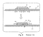
- Fig. 6 is a schematic view intended to explain the condition of the substrate in a heating step shown in Part (d) of Fig. 5 .
- thermoset adhesive 93p being hardened is fluidized along with the deformation of the film 911, air bubbles occur within the thermoset adhesive 93p and remain as voids 931 even after the thermoset adhesive 93p has hardened.
- the voids within the hardened thermoset adhesive 93p decrease adhesion strength between the IC chip 92 and the substrate 91, thereby degrading the reliability of the RFID tag.
- the problem of reliability degradation due to the occurrence of such voids as described above is not limited to RFID tags but is common to electronic devices wherein a circuit chip is mounted on a film-like substrate.
- the present invention has been made in view of the above circumstances and provides an electronic device having reliability enhanced by suppressing the occurrence of voids and a method of manufacturing the electronic device.
- the substrate may be clamped by the presser section and the support section in the step of heating.
- the film is prevented from becoming deformed when being melted by heating since the surface of the film abutting on the support section has been roughened and, therefore, frictional force against the deviational movement of the film increases. Consequently, voids due to film deformation are prevented from being produced within the thermoset adhesive, thereby enhancing the reliability of the electronic device.
- manufacturing costs decrease since the production yield of the electronic device improves.
- the support section has a surface abutting on the film and being coarser than the film prior to being roughened in the step of roughening.
- the electronic device is an RFID tag that makes the conductor pattern function as a communications antenna and carries out wireless communication via the conductor pattern using the circuit chip.
- the method of manufacturing an electronic device is suitable for the manufacture of RFID tags.
- the electronic device in accordance with an embodiment of the present invention includes:
- thermoset adhesive Since the film of the electronic device has been surface-roughened, the film is prevented from becoming deformed when heating by clamping the film side and the circuit chip side thereof by a heating apparatus in a manufacturing process. Consequently, according to the electronic device, reliability increases since there are fewer voids in the thermoset adhesive.
- the conductor pattern functions as a communications antenna and the circuit chip carries out wireless communication via the conductor pattern.
- an electronic device having reliability enhanced by preventing voids from being produced and a method of manufacturing the electronic device.
- Fig. 1 is a perspective view illustrating an RFID tag in accordance with one embodiment of the present invention.
- the RFID tag 1 shown in Fig. 1 includes a substrate 11 wherein a metal antenna pattern 112 is formed on a film 111 made of a PET material, an IC chip 12 mounted on the substrate 11, and a thermoset adhesive 13 for joining the substrate 11 and the IC chip 12.
- a substrate 11 wherein a metal antenna pattern 112 is formed on a film 111 made of a PET material, an IC chip 12 mounted on the substrate 11, and a thermoset adhesive 13 for joining the substrate 11 and the IC chip 12.
- an underside surface 11b opposite to a mounting surface 11a on which the IC chip 12 is mounted is surface-roughened as described later.
- the RFID tag 1 of the present embodiment is an electronic device which contactlessly exchanges information with a reader/writer not shown in the figure.
- the RFID tag 1 receives electromagnetic field energy emitted by the reader/writer at the antenna pattern 112 as electric energy by which the IC chip 12 is driven.
- the antenna pattern 112 functions as a communications antenna and the IC chip 12 carries out wireless communication via the antenna pattern 112.
- the RFID tag 1 corresponds to one example of the electronic device according to the present invention
- the antenna pattern 112 corresponds to one example of the conductor pattern according to the present invention
- the IC chip 12 corresponds to one example of the circuit chip according to the present invention.
- the RFID tag used in the present application may be considered as an internal constituent member (inlay) for RFID tags and therefore may, in some cases, be referred to as an inlay for RFID tags among persons skilled in the technical filed of the present application.
- the RFID tag may be referred to as a wireless IC tag.
- a contactless IC card is included in the RFID tag.
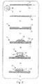
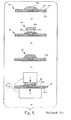
- Figs. 2 and 3 are schematic views illustrating steps of manufacturing an RFID tag in accordance with one embodiment of the present invention.
- Fig. 2 respective steps of manufacturing the RFID tag 1 are sequentially shown in Farts (a) to (f) of the figure, whereas in Fig. 3 , steps subsequent to the steps of Fig. 2 are sequentially shown in Parts (g) and (h) of the figure.
- the dimension in the thickness direction of the RFID tag 1 and the IC chip 12 are represented more exaggeratingly than those shown in Fig. 1 .
- a film 111 made of a PET material is first prepared in a surface-roughening step shown in Part (a) of Fig. 2 , an underside surface 11b opposite to a mounting surface 11a on which an IC chip is to be mounted is mechanically ground using a grinding apparatus S.
- the underside surface 11b of the film 111 is surface-roughened as shown in Part (b) of Fig. 2 .
- the antenna pattern 112 is formed on the mounting surface 11a of the film 111. While the antenna pattern 112 is formed by forming a copper layer on the film 111 and a resist layer thereon and etching the resist layer, it is also possible to adopt other methods, such as silver paste printing, as a specific method of forming the antenna pattern 112. In the conductor-forming step shown in Part (c) of Fig. 2 , there is obtained the substrate 11 wherein the antenna pattern 112 is formed on the film 111 made of a PET material.
- thermoset adhesive 13p in liquid form is attached onto the substrate 11.
- the thermoset adhesive i3p is applied to an area, among the areas of the mounting surface 11a of the substrate 11 whereon the antenna pattern 1 12 is formed, in which the IC chip 12 is to be mounted and to the periphery of the area.
- the IC chip 12 is placed on a part of the substrate 11 to which the thermoset adhesive 13p is attached.
- the IC chip 12 is mounted on the substrate 11 using a flip-chip technique. That is, the IC chip 12 is mounted on the substrate 11 via the thermoset adhesive 13p, while being positioned so that a surface 12a thereof whereon a circuit is formed faces the substrate 11.
- the IC chip 12 is mounted on the substrate 11 with the bumps 121 positionally aligned with the antenna pattern 112.
- the substrate 11 whereon the IC chip 12 is mounted is clamped by a heating apparatus 2 from both the film 111 side and the IC chip 12 side of the substrate 11.
- the heating apparatus 2 has a heating head 21 and a heating stage 22 for clamping the substrate 11.
- the heating head 21 contains a heater not shown in the figure.
- the heating head 21 abuts on the IC chip 12 and the heating stage 22 abuts on the film 111.
- the heating head 21 corresponds to one example of the presser section according to the present invention
- the heating stage 22 corresponds to one example of the support section according to the present invention.
- Fig. 4 is a perspective view schematically illustrating a structure of the heating apparatus.
- the heating stage 22 that the heating apparatus 2 is provided with is such that a surface 22a thereof abutting on the film 111 is surface-roughened so as to be coarser than the film 111 prior to being subjected to the surface-roughening step shown in Part (a) of Fig. 2 .
- the substrate 11 whereon the IC chip 12 is mounted is clamped by the heating stage 22 and the heating head 21 in the clamping step shown in Part (g) of Fig. 3 . Consequently, the bumps 121 come into a state of sure contact with the antenna pattern 112.
- the heating head 21 is made to generate heat so that the thermoset adhesive 13p is heated and hardened.
- the IC chip 12 is fixed to the substrate 11 with the bumps 121 in contact with the antenna pattern 112.
- the underside surface 11b of the surface-roughened film 111 abuts on the heating stage 22.
- the surface 22a of the heating stage 22 on which the film 111 abuts is coarser than the underside surface 11b of the film 111 prior to being subjected to the surface-roughening step.
- thermoset adhesive 13p there is provided even greater frictional force against the deviational movement of the film 111, thereby preventing the film 111 from becoming deformed even when melted by heating. Accordingly, voids due to film deformation are prevented from being produced within the thermoset adhesive 13p.
- the present invention is not limited to a manufacturing method intended for an RFID tag, as long as the method is directed at manufacturing an electronic device wherein a circuit chip is mounted on a film-like substrate.
- the present invention is also applied to, for example, a method of manufacturing an ultra-thin IC card and a method of manufacturing a printed circuit board device wherein a circuit chip is fixed with a thermoset adhesive onto a flexible printed circuit (FPC) used as a substrate.
- FPC flexible printed circuit
- the present invention is not limited to this case.
- the surface-roughening step may be, for example, such that surface-roughening is carried out by means of treatment in a plasma atmosphere or by means of chemical treatment using chemicals.
- the film composing the substrate of the RFID tag is made of a PET material
- the film of the electronic device targeted by the present invention is not limited to the PET material but may be made of a material selected from a group consisting of a polyester material, a polyolefin material, a polycarbonate material, an acrylic material, and the like.
- the presser section of the present invention is combined with a heating source, and that the heating stage does not generate heat
- the present invention is not limited to this case.
- the heating source may be combined with the support section, or may be provided as a part independent of the presser section and the support section.
Landscapes
- Engineering & Computer Science (AREA)
- Manufacturing & Machinery (AREA)
- Microelectronics & Electronic Packaging (AREA)
- Credit Cards Or The Like (AREA)
- Wire Bonding (AREA)
- Encapsulation Of And Coatings For Semiconductor Or Solid State Devices (AREA)
- Electric Connection Of Electric Components To Printed Circuits (AREA)
Abstract
Description
- The present invention relates to an electronic device and a method of manufacturing the electronic device and, more particularly, to an electronic device wherein a circuit chip is mounted on a film-like substrate and a method of manufacturing the electronic device.
- Conventionally, there is widely known an electronic device wherein a circuit chip is mounted on a substrate, such as a printed wiring substrate. This electronic device is used in such applications where it is built into an electronic apparatus to control the apparatus or is operated on a stand-alone basis to exchange information with an external apparatus. As an example of the electronic device, there are known various types of radio frequency identification (RFID) tags for contactlessly exchanging information with an external apparatus as typified by a reader/writer, using radio waves. As a type of these RFID tags, there has been proposed an RFID tag wherein a conductor pattern and an IC chip for radio communication are mounted on a base sheet. It has been conceived to use this type of RFID tag in such a manner that the tag is attached to an article or the like to, for example, identify the article by exchanging information about the article with an external apparatus.
- There is a demand to reduce the size and weight of RFID tags and, in particular, to make them thinner, more flexible and less costly. In response to this demand, there has been proposed an RFID tag employing a film made of, for example, a resin material, such as polyethylene-terephthalate (PET), as a material of a substrate on which an IC chip is mounted (For example, see
Japanese Patent Laid-Open No. 2001-156110 -
Fig. 5 is a schematic view intended to explain a method of manufacturing an RFID tag in a conventional technique. -
Fig. 5 sequentially shows in Parts (a) to (d) thereof respective steps for manufacturing an RFID tag. - In order to manufacture an RFID tag, there is first prepared a
substrate 91 wherein aconductor pattern 912 functioning as an antenna of the RFID tag is formed on afilm 911 made of PET, and then athermoset adhesive 93p which is hardened by heating is attached onto thissubstrate 91, as shown in Part (a) ofFig. 5 . - Next, as shown in Part (b) of
Fig. 5 , anIC chip 92 is mounted on thesubstrate 91 in a part to which thethermoset adhesive 93p has been attached.Bumps 921 to be connected to theconductor pattern 912 are formed on theIC chip 92. As shown in Part (c) ofFig. 5 , theIC chip 92 is mounted on thesubstrate 91 so that thebumps 921 positionally align with theconductor pattern 912. - Next, as shown in Part (d) of
Fig. 5 , thesubstrate 91 whereon theIC chip 92 is mounted is clamped by aheating apparatus 8 from both thefilm 911 side and theIC chip 92 side of thesubstrate 91, with a supportingstage 82 and aheating head 81 of the heating apparatus 80, respectively. Then, thethermoset adhesive 93p is heated and hardened by theheating head 81 of theheating apparatus 8 abutting on theIC chip 92 side. In this way, theIC chip 92 is fixed to thesubstrate 91 with thebumps 921 in contact with theconductor pattern 912, thereby completing a small-sized lightweight RFID tag. - However, since the glass transition point of PET, which is the material of the
film 911, is approximately 67°C and, wherefore, the upper temperature limit of PET is low, thefilm 911 is liable to deformation due to heating applied when hardening thethermoset adhesive 93p. -
Fig. 6 is a schematic view intended to explain the condition of the substrate in a heating step shown in Part (d) ofFig. 5 . - If a heating treatment is carried out with the
IC chip 92 mounted on thesubstrate 91 as shown in Part (a) ofFig. 6 , the temperature of thesubstrate 91 rises and thefilm 911 becomes deformed, as shown in Part (b) ofFig. 6 . If thethermoset adhesive 93p being hardened is fluidized along with the deformation of thefilm 911, air bubbles occur within thethermoset adhesive 93p and remain asvoids 931 even after thethermoset adhesive 93p has hardened. The voids within the hardenedthermoset adhesive 93p decrease adhesion strength between theIC chip 92 and thesubstrate 91, thereby degrading the reliability of the RFID tag. - The problem of reliability degradation due to the occurrence of such voids as described above is not limited to RFID tags but is common to electronic devices wherein a circuit chip is mounted on a film-like substrate.
- The present invention has been made in view of the above circumstances and provides an electronic device having reliability enhanced by suppressing the occurrence of voids and a method of manufacturing the electronic device.
- A method of manufacturing an electronic device according to an embodiment of the present invention includes the steps of:
- roughening an underside surface of a film made of a resin material, which is opposite to a mounting surface of the film, the mounting surface being a surface on which, a circuit chip is to be mounted;
- forming a conductor pattern on the mounting surface of the film, thereby obtaining a substrate made of the film on which the conductor pattern is formed;
- attaching a thermoset adhesive to a surface of the substrate, on which surface the conductor pattern is formed;
- mounting the circuit chip to be connected to the conductor pattern on the substrate via the thermoset adhesive;
- clamping the substrate by a heating apparatus having a presser section and a support section for heating the thermoset adhesive, such that the presser section abuts on the circuit chip mounted on the substrate and the support section abuts on the underside surface of the film roughened in the step of roughening; and
- fixing the circuit chip to the conductor pattern by heating and hardening the thermoset adhesive using the heating apparatus.
- In the method of manufacturing an electronic device, the substrate may be clamped by the presser section and the support section in the step of heating. At this time, the film is prevented from becoming deformed when being melted by heating since the surface of the film abutting on the support section has been roughened and, therefore, frictional force against the deviational movement of the film increases. Consequently, voids due to film deformation are prevented from being produced within the thermoset adhesive, thereby enhancing the reliability of the electronic device. In addition, manufacturing costs decrease since the production yield of the electronic device improves.
- In the method of manufacturing an electronic device, preferably, the support section has a surface abutting on the film and being coarser than the film prior to being roughened in the step of roughening.
- As the result of not only the film on the manufactured side but also the surface of the support section of an apparatus on the manufacturing side being roughened, frictional force against the deviational movement of the film increases further, thereby further preventing the film from becoming deformed when being melted by heating.
- In addition, in the method of manufacturing an electronic device, preferably, the electronic device is an RFID tag that makes the conductor pattern function as a communications antenna and carries out wireless communication via the conductor pattern using the circuit chip.
- In order to meet requirements for miniaturization and flexibility, there is a demand to make thinner the film of RFID tags attached to merchandise or cards when they are in use. The method of manufacturing an electronic device is suitable for the manufacture of RFID tags.
- Furthermore, the electronic device in accordance with an embodiment of the present invention includes:
- a substrate in which a conductor pattern is formed on a film made of a resin material and a surface of the substrate opposite to a surface whereon the conductor pattern is formed is roughened; and
- a circuit chip mounted on the substrate via a thermoset adhesive and electrically connected to the conductor pattern.
- Since the film of the electronic device has been surface-roughened, the film is prevented from becoming deformed when heating by clamping the film side and the circuit chip side thereof by a heating apparatus in a manufacturing process. Consequently, according to the electronic device, reliability increases since there are fewer voids in the thermoset adhesive.
- It should not here that in the electronic device, preferably, the conductor pattern functions as a communications antenna and the circuit chip carries out wireless communication via the conductor pattern.
- As heretofore described, according to embodiments of the present invention, there are realized an electronic device having reliability enhanced by preventing voids from being produced and a method of manufacturing the electronic device.
- Embodiments of the present invention will be described in detail based on the following figures, wherein:
-
Fig. 1 is a perspective view illustrating an RFID tag in accordance with one embodiment of the present invention; -
Fig. 2 is a schematic view illustrating a process of manufacturing an RFID tag in accordance with one embodiment of the present invention; -
Fig. 3 is a schematic view illustrating a process subsequent to the process illustrated inFig. 2 ; -
Fig. 4 is a perspective view schematically illustrating a structure of a heating apparatus; -
Fig. 5 is a schematic view intended to explain a method of manufacturing an RFID tag in a conventional technique; and -
Fig. 6 is a schematic view intended to explain the condition of the substrate in a heating step shown inFig. 5 . - Hereinafter, embodiments of the present invention will be described with reference to the accompanying drawings.
-
Fig. 1 is a perspective view illustrating an RFID tag in accordance with one embodiment of the present invention. - The RFID tag 1 shown in
Fig. 1 includes asubstrate 11 wherein ametal antenna pattern 112 is formed on afilm 111 made of a PET material, anIC chip 12 mounted on thesubstrate 11, and athermoset adhesive 13 for joining thesubstrate 11 and theIC chip 12. Of the two surfaces of thesubstrate 11, anunderside surface 11b opposite to amounting surface 11a on which theIC chip 12 is mounted is surface-roughened as described later. - The RFID tag 1 of the present embodiment is an electronic device which contactlessly exchanges information with a reader/writer not shown in the figure. The RFID tag 1 receives electromagnetic field energy emitted by the reader/writer at the
antenna pattern 112 as electric energy by which theIC chip 12 is driven. Theantenna pattern 112 functions as a communications antenna and theIC chip 12 carries out wireless communication via theantenna pattern 112. - Note here that the RFID tag 1 corresponds to one example of the electronic device according to the present invention, the
antenna pattern 112 corresponds to one example of the conductor pattern according to the present invention, and theIC chip 12 corresponds to one example of the circuit chip according to the present invention. - Also note that the RFID tag used in the present application may be considered as an internal constituent member (inlay) for RFID tags and therefore may, in some cases, be referred to as an inlay for RFID tags among persons skilled in the technical filed of the present application. Alternatively, the RFID tag may be referred to as a wireless IC tag. In addition, a contactless IC card is included in the RFID tag.
- Hereinafter, a method of manufacturing the RFID tag 1 will be described.
-
Figs. 2 and3 are schematic views illustrating steps of manufacturing an RFID tag in accordance with one embodiment of the present invention. - In
Fig. 2 , respective steps of manufacturing the RFID tag 1 are sequentially shown in Farts (a) to (f) of the figure, whereas inFig. 3 , steps subsequent to the steps ofFig. 2 are sequentially shown in Parts (g) and (h) of the figure. For ease of viewing the figures, the dimension in the thickness direction of the RFID tag 1 and theIC chip 12 are represented more exaggeratingly than those shown inFig. 1 . - In order to manufacture the RFID tag 1, a
film 111 made of a PET material is first prepared in a surface-roughening step shown in Part (a) ofFig. 2 , anunderside surface 11b opposite to a mountingsurface 11a on which an IC chip is to be mounted is mechanically ground using a grinding apparatus S. Thus, theunderside surface 11b of thefilm 111 is surface-roughened as shown in Part (b) ofFig. 2 . - Next, in a conductor-forming step shown in Part (c) of
Fig. 2 , theantenna pattern 112 is formed on the mountingsurface 11a of thefilm 111. While theantenna pattern 112 is formed by forming a copper layer on thefilm 111 and a resist layer thereon and etching the resist layer, it is also possible to adopt other methods, such as silver paste printing, as a specific method of forming theantenna pattern 112. In the conductor-forming step shown in Part (c) ofFig. 2 , there is obtained thesubstrate 11 wherein theantenna pattern 112 is formed on thefilm 111 made of a PET material. - Next, in an adhesion step shown in Part (d) of
Fig. 2 , a thermoset adhesive 13p in liquid form is attached onto thesubstrate 11. The thermoset adhesive i3p is applied to an area, among the areas of the mountingsurface 11a of thesubstrate 11 whereon the antenna pattern 1 12 is formed, in which theIC chip 12 is to be mounted and to the periphery of the area. - Next, in a mounting step shown in Parts (e) and (f) of
Fig. 2 , theIC chip 12 is placed on a part of thesubstrate 11 to which the thermoset adhesive 13p is attached. TheIC chip 12 is mounted on thesubstrate 11 using a flip-chip technique. That is, theIC chip 12 is mounted on thesubstrate 11 via the thermoset adhesive 13p, while being positioned so that asurface 12a thereof whereon a circuit is formed faces thesubstrate 11. On thesurface 12a whereon the circuit of theIC chip 12 is formed, there are formedbumps 121 to be connected to theantenna pattern 112. As shown in Part (f) ofFig. 2 , theIC chip 12 is mounted on thesubstrate 11 with thebumps 121 positionally aligned with theantenna pattern 112. - Next, in a clamping step shown in Part (g) of
Fig. 2 , thesubstrate 11 whereon theIC chip 12 is mounted is clamped by aheating apparatus 2 from both thefilm 111 side and theIC chip 12 side of thesubstrate 11. Theheating apparatus 2 has aheating head 21 and aheating stage 22 for clamping thesubstrate 11. Theheating head 21 contains a heater not shown in the figure. In the clamping step, theheating head 21 abuts on theIC chip 12 and theheating stage 22 abuts on thefilm 111. Theheating head 21 corresponds to one example of the presser section according to the present invention, and theheating stage 22 corresponds to one example of the support section according to the present invention. -
Fig. 4 is a perspective view schematically illustrating a structure of the heating apparatus. - The
heating stage 22 that theheating apparatus 2 is provided with is such that asurface 22a thereof abutting on thefilm 111 is surface-roughened so as to be coarser than thefilm 111 prior to being subjected to the surface-roughening step shown in Part (a) ofFig. 2 . - Referring back to
Fig. 3 to continue explanation, thesubstrate 11 whereon theIC chip 12 is mounted is clamped by theheating stage 22 and theheating head 21 in the clamping step shown in Part (g) ofFig. 3 . Consequently, thebumps 121 come into a state of sure contact with theantenna pattern 112. - Next, in the heating step shown in Part (h) of
Fig. 3 , theheating head 21 is made to generate heat so that the thermoset adhesive 13p is heated and hardened. As the result of the thermoset adhesive 13p being hardened, theIC chip 12 is fixed to thesubstrate 11 with thebumps 121 in contact with theantenna pattern 112. In this heating step, theunderside surface 11b of the surface-roughenedfilm 111 abuts on theheating stage 22. In addition, thesurface 22a of theheating stage 22 on which thefilm 111 abuts is coarser than theunderside surface 11b of thefilm 111 prior to being subjected to the surface-roughening step. Accordingly, there is provided even greater frictional force against the deviational movement of thefilm 111, thereby preventing thefilm 111 from becoming deformed even when melted by heating. Accordingly, voids due to film deformation are prevented from being produced within the thermoset adhesive 13p. - When the heating step shown in Part (h) of
Fig. 3 is finished, the RFID tag 1 (seeFig. 1 ) is completed. - While an explanation has been made of a method of manufacturing an RFID tag and an example of a heating apparatus in the above-described embodiment, the present invention is not limited to a manufacturing method intended for an RFID tag, as long as the method is directed at manufacturing an electronic device wherein a circuit chip is mounted on a film-like substrate. The present invention is also applied to, for example, a method of manufacturing an ultra-thin IC card and a method of manufacturing a printed circuit board device wherein a circuit chip is fixed with a thermoset adhesive onto a flexible printed circuit (FPC) used as a substrate.
- Furthermore, while in the above-described embodiment, an explanation has been made on the premise that the
underside surface 11b of thefilm 111 is mechanically ground using the grinding apparatus S in the surface-roughening step, , the present invention is not limited to this case. Alternatively, the surface-roughening step may be, for example, such that surface-roughening is carried out by means of treatment in a plasma atmosphere or by means of chemical treatment using chemicals. - In addition, while in the above-described embodiment, an explanation has been made on the premise that the film composing the substrate of the RFID tag is made of a PET material, the film of the electronic device targeted by the present invention is not limited to the PET material but may be made of a material selected from a group consisting of a polyester material, a polyolefin material, a polycarbonate material, an acrylic material, and the like.
- While in the above-described embodiment, an explanation has been made on the premise that the presser section of the present invention is combined with a heating source, and that the heating stage does not generate heat, the present invention is not limited to this case. Alternatively, the heating source may be combined with the support section, or may be provided as a part independent of the presser section and the support section.
Claims (5)
- A method of manufacturing an electronic device, comprising the steps of:roughening an underside surface of a film made of a resin material, which is opposite to a mounting surface of the film, the mounting surface being a surface on which a circuit chip is to be mounted;forming a conductor pattern on the mounting surface of the film, thereby obtaining a substrate made of the film on which the conductor pattern is formed;attaching a thermoset adhesive to a surface of the substrate, on which surface the conductor pattern is formed;mounting the circuit chip to be connected to the conductor pattern on the substrate via the thermoset adhesive;clamping the substrate by a heating apparatus having a presser section and a support section for heating the thermoset adhesive, such that the presser section abuts on the circuit chip mounted on the substrate and the support section abuts on the underside surface of the film roughened in the step of roughening; andfixing the circuit chip to the conductor pattern by heating and hardening the thermoset adhesive using the heating apparatus.
- The method of manufacturing an electronic device according to claim 1, wherein the support section has a surface abutting on the film and being coarser than the film prior to being roughened in the step of roughening.
- The method of manufacturing an electronic device according to any preceding claim, wherein the electronic device is an RFID tag that makes the conductor pattern function as a communications antenna and carries out wireless communication via the conductor pattern using the circuit chip.
- An electronic device comprising:a substrate in which a conductor pattern is formed on a film made of a resin material and a surface of the substrate opposite to a surface whereon the conductor pattern is formed is roughened; anda circuit chip mounted on the substrate via a thermoset adhesive and electrically connected to the conductor pattern.
- The electronic device according to claim 4, wherein the conductor pattern functions as a communications antenna, and
the circuit chip carries out wireless communication via the conductor pattern.
Applications Claiming Priority (1)
| Application Number | Priority Date | Filing Date | Title |
|---|---|---|---|
| JP2007009261A JP5029026B2 (en) | 2007-01-18 | 2007-01-18 | Manufacturing method of electronic device |
Publications (3)
| Publication Number | Publication Date |
|---|---|
| EP1947918A2 true EP1947918A2 (en) | 2008-07-23 |
| EP1947918A3 EP1947918A3 (en) | 2009-10-14 |
| EP1947918B1 EP1947918B1 (en) | 2010-10-13 |
Family
ID=39387240
Family Applications (1)
| Application Number | Title | Priority Date | Filing Date |
|---|---|---|---|
| EP07121152A Not-in-force EP1947918B1 (en) | 2007-01-18 | 2007-11-20 | Electronic device and method of manufacturing same |
Country Status (7)
| Country | Link |
|---|---|
| US (1) | US8356406B2 (en) |
| EP (1) | EP1947918B1 (en) |
| JP (1) | JP5029026B2 (en) |
| KR (1) | KR100923943B1 (en) |
| CN (1) | CN100593364C (en) |
| DE (1) | DE602007009785D1 (en) |
| TW (1) | TWI336223B (en) |
Families Citing this family (1)
| Publication number | Priority date | Publication date | Assignee | Title |
|---|---|---|---|---|
| CN111541020B (en) * | 2020-05-08 | 2021-08-10 | 北京航空航天大学 | Antenna based on liquid-gas phase change actuator and preparation method thereof |
Family Cites Families (36)
| Publication number | Priority date | Publication date | Assignee | Title |
|---|---|---|---|---|
| JPS57128948A (en) | 1981-02-02 | 1982-08-10 | Sharp Corp | Electronic part |
| JPS60236250A (en) | 1984-05-10 | 1985-11-25 | Toshiba Corp | Manufacture of ic card |
| JPS62216259A (en) * | 1986-03-17 | 1987-09-22 | Fujitsu Ltd | Manufacture and structure of hybrid integrated circuit |
| US6303873B1 (en) * | 1995-10-31 | 2001-10-16 | Ibiden Co., Ltd. | Electronic part module and process for manufacturing the same |
| US5872338A (en) * | 1996-04-10 | 1999-02-16 | Prolinx Labs Corporation | Multilayer board having insulating isolation rings |
| JPH1041694A (en) * | 1996-07-25 | 1998-02-13 | Sharp Corp | Substrate mounting structure of semiconductor element and mounting method thereof |
| KR100328807B1 (en) * | 1998-05-08 | 2002-03-14 | 가네코 히사시 | Resin structure in which manufacturing cost is cheap and sufficient adhesive strength can be obtained and method of manufacturing it |
| WO2000002243A1 (en) * | 1998-07-01 | 2000-01-13 | Seiko Epson Corporation | Semiconductor device, method of manufacture, circuit board, and electronic device |
| KR100855529B1 (en) * | 1998-09-03 | 2008-09-01 | 이비덴 가부시키가이샤 | Multilayer printed wiring board and method for manufacturing the same |
| JP2000138387A (en) | 1998-10-29 | 2000-05-16 | Dainippon Printing Co Ltd | Surface protection sheet for solar cell module and solar cell module using the same |
| US6117059A (en) * | 1998-11-07 | 2000-09-12 | Branson Ultrasonics Corporation | Method of manufacturing a filtration bag |
| US6353420B1 (en) * | 1999-04-28 | 2002-03-05 | Amerasia International Technology, Inc. | Wireless article including a plural-turn loop antenna |
| KR100940764B1 (en) * | 1999-09-14 | 2010-02-10 | 소니 케미카루 앤드 인포메이션 디바이스 가부시키가이샤 | Anisotropic conductive connector and manufacturing method |
| JP3365367B2 (en) * | 1999-09-14 | 2003-01-08 | ソニーケミカル株式会社 | COG mounting products and connection materials |
| US6421013B1 (en) * | 1999-10-04 | 2002-07-16 | Amerasia International Technology, Inc. | Tamper-resistant wireless article including an antenna |
| JP3451373B2 (en) * | 1999-11-24 | 2003-09-29 | オムロン株式会社 | Manufacturing method of data carrier capable of reading electromagnetic wave |
| EP1143378A1 (en) * | 2000-04-04 | 2001-10-10 | Smartag (S) Pte. Ltd. | Method for manufacturing of RFID inlet |
| WO2002056378A1 (en) * | 2001-01-11 | 2002-07-18 | Matsushita Electric Industrial Co., Ltd. | Circuit board and production method therefor |
| JP3866058B2 (en) * | 2001-07-05 | 2007-01-10 | シャープ株式会社 | Semiconductor device, wiring board and tape carrier |
| JP2003141486A (en) | 2001-11-08 | 2003-05-16 | Oji Paper Co Ltd | Non-contact IC card and method of manufacturing the same |
| JP3791431B2 (en) * | 2002-02-26 | 2006-06-28 | セイコーエプソン株式会社 | Mounting structure manufacturing equipment |
| JP3823845B2 (en) * | 2002-02-26 | 2006-09-20 | セイコーエプソン株式会社 | Mounting structure |
| JP4606709B2 (en) | 2003-07-11 | 2011-01-05 | アスリートFa株式会社 | Electronic component bonding method and electronic component bonding apparatus |
| JP3533665B1 (en) * | 2002-12-17 | 2004-05-31 | オムロン株式会社 | A method for manufacturing an electronic component module and a method for manufacturing a data carrier capable of reading electromagnetic waves. |
| JP4065799B2 (en) * | 2003-03-12 | 2008-03-26 | 株式会社ルネサステクノロジ | Ultrasonic bonding apparatus and method |
| JP4567988B2 (en) * | 2004-02-05 | 2010-10-27 | 株式会社日立製作所 | Paper-like RFID tag and manufacturing method thereof |
| US7090946B2 (en) * | 2004-02-19 | 2006-08-15 | Maxwell Technologies, Inc. | Composite electrode and method for fabricating same |
| JP4791708B2 (en) * | 2004-06-23 | 2011-10-12 | リンテック株式会社 | Adhesive resin material for mounting electronic components, electronic device using the same, and method for producing the adhesive resin material for mounting electronic components |
| JP4385895B2 (en) * | 2004-08-26 | 2009-12-16 | カシオ計算機株式会社 | Bonding equipment |
| JP4676196B2 (en) * | 2004-12-16 | 2011-04-27 | 富士通株式会社 | RFID tag |
| JP2006253269A (en) | 2005-03-09 | 2006-09-21 | Mitsui Mining & Smelting Co Ltd | Printed wiring board, semiconductor device and plasma display device |
| JP4750450B2 (en) * | 2005-04-05 | 2011-08-17 | 富士通株式会社 | RFID tag |
| JP2008040904A (en) * | 2006-08-08 | 2008-02-21 | Hitachi Ltd | RFID tag and reading method thereof |
| US20080149371A1 (en) * | 2006-12-22 | 2008-06-26 | Angstrom Power Inc. | Flexible circuit |
| JP2008177351A (en) * | 2007-01-18 | 2008-07-31 | Fujitsu Ltd | Electronic device and method for manufacturing electronic device |
| JP4860494B2 (en) * | 2007-01-18 | 2012-01-25 | 富士通株式会社 | Manufacturing method of electronic device |
-
2007
- 2007-01-18 JP JP2007009261A patent/JP5029026B2/en not_active Expired - Fee Related
- 2007-11-13 TW TW096142827A patent/TWI336223B/en not_active IP Right Cessation
- 2007-11-13 US US11/983,931 patent/US8356406B2/en not_active Expired - Fee Related
- 2007-11-20 DE DE602007009785T patent/DE602007009785D1/en active Active
- 2007-11-20 EP EP07121152A patent/EP1947918B1/en not_active Not-in-force
- 2007-12-06 KR KR1020070126036A patent/KR100923943B1/en not_active Expired - Fee Related
- 2007-12-07 CN CN200710195966A patent/CN100593364C/en not_active Expired - Fee Related
Also Published As
| Publication number | Publication date |
|---|---|
| JP5029026B2 (en) | 2012-09-19 |
| EP1947918B1 (en) | 2010-10-13 |
| KR100923943B1 (en) | 2009-10-29 |
| US8356406B2 (en) | 2013-01-22 |
| KR20080068529A (en) | 2008-07-23 |
| TWI336223B (en) | 2011-01-11 |
| DE602007009785D1 (en) | 2010-11-25 |
| EP1947918A3 (en) | 2009-10-14 |
| CN101227799A (en) | 2008-07-23 |
| JP2008177349A (en) | 2008-07-31 |
| US20090114435A1 (en) | 2009-05-07 |
| CN100593364C (en) | 2010-03-03 |
| TW200833205A (en) | 2008-08-01 |
Similar Documents
| Publication | Publication Date | Title |
|---|---|---|
| EP1956873B1 (en) | RFID tag and method of manufacturing the same | |
| US20080202678A1 (en) | Production method of electronic apparatus, production method of electronic equipment in which electronic apparatus is packaged, and production method of article in which electronic apparatus is mounted | |
| EP2063383A1 (en) | RFID tag and method of manufacturing the same | |
| KR100945771B1 (en) | Manufacturing method of electronic device | |
| CN100481122C (en) | RFID tag and method of manufacturing the same | |
| EP1947918B1 (en) | Electronic device and method of manufacturing same | |
| CN100416606C (en) | Radio frequency identification tag, module assembly and method for manufacturing radio frequency identification tag | |
| JP2008177350A (en) | Electronic device manufacturing method and manufacturing apparatus | |
| JP2000137781A (en) | Card type electronic circuit board and method of manufacturing the same | |
| JP4085790B2 (en) | IC card manufacturing method | |
| KR20080084767A (en) | Electronic card module and its manufacturing method | |
| EP2053548A1 (en) | RFID tag and manufacturing method thereof | |
| JP2003203944A (en) | Non-contact communication device module and method of manufacturing the same | |
| JP2021140671A (en) | RFID inlay |
Legal Events
| Date | Code | Title | Description |
|---|---|---|---|
| PUAI | Public reference made under article 153(3) epc to a published international application that has entered the european phase |
Free format text: ORIGINAL CODE: 0009012 |
|
| AK | Designated contracting states |
Kind code of ref document: A2 Designated state(s): AT BE BG CH CY CZ DE DK EE ES FI FR GB GR HU IE IS IT LI LT LU LV MC MT NL PL PT RO SE SI SK TR |
|
| AX | Request for extension of the european patent |
Extension state: AL BA HR MK RS |
|
| PUAL | Search report despatched |
Free format text: ORIGINAL CODE: 0009013 |
|
| AK | Designated contracting states |
Kind code of ref document: A3 Designated state(s): AT BE BG CH CY CZ DE DK EE ES FI FR GB GR HU IE IS IT LI LT LU LV MC MT NL PL PT RO SE SI SK TR |
|
| AX | Request for extension of the european patent |
Extension state: AL BA HR MK RS |
|
| 17P | Request for examination filed |
Effective date: 20091230 |
|
| GRAP | Despatch of communication of intention to grant a patent |
Free format text: ORIGINAL CODE: EPIDOSNIGR1 |
|
| AKX | Designation fees paid |
Designated state(s): DE FR GB |
|
| GRAS | Grant fee paid |
Free format text: ORIGINAL CODE: EPIDOSNIGR3 |
|
| GRAA | (expected) grant |
Free format text: ORIGINAL CODE: 0009210 |
|
| AK | Designated contracting states |
Kind code of ref document: B1 Designated state(s): DE FR GB |
|
| REG | Reference to a national code |
Ref country code: GB Ref legal event code: FG4D |
|
| REF | Corresponds to: |
Ref document number: 602007009785 Country of ref document: DE Date of ref document: 20101125 Kind code of ref document: P |
|
| PLBE | No opposition filed within time limit |
Free format text: ORIGINAL CODE: 0009261 |
|
| STAA | Information on the status of an ep patent application or granted ep patent |
Free format text: STATUS: NO OPPOSITION FILED WITHIN TIME LIMIT |
|
| 26N | No opposition filed |
Effective date: 20110714 |
|
| REG | Reference to a national code |
Ref country code: DE Ref legal event code: R097 Ref document number: 602007009785 Country of ref document: DE Effective date: 20110714 |
|
| PGFP | Annual fee paid to national office [announced via postgrant information from national office to epo] |
Ref country code: GB Payment date: 20131120 Year of fee payment: 7 Ref country code: FR Payment date: 20131108 Year of fee payment: 7 Ref country code: DE Payment date: 20131113 Year of fee payment: 7 |
|
| REG | Reference to a national code |
Ref country code: DE Ref legal event code: R119 Ref document number: 602007009785 Country of ref document: DE |
|
| GBPC | Gb: european patent ceased through non-payment of renewal fee |
Effective date: 20141120 |
|
| REG | Reference to a national code |
Ref country code: FR Ref legal event code: ST Effective date: 20150731 |
|
| PG25 | Lapsed in a contracting state [announced via postgrant information from national office to epo] |
Ref country code: GB Free format text: LAPSE BECAUSE OF NON-PAYMENT OF DUE FEES Effective date: 20141120 Ref country code: DE Free format text: LAPSE BECAUSE OF NON-PAYMENT OF DUE FEES Effective date: 20150602 |
|
| PG25 | Lapsed in a contracting state [announced via postgrant information from national office to epo] |
Ref country code: FR Free format text: LAPSE BECAUSE OF NON-PAYMENT OF DUE FEES Effective date: 20141201 |