EP1947689A2 - High temperature fine grain aluminium heater - Google Patents
High temperature fine grain aluminium heater Download PDFInfo
- Publication number
- EP1947689A2 EP1947689A2 EP08000957A EP08000957A EP1947689A2 EP 1947689 A2 EP1947689 A2 EP 1947689A2 EP 08000957 A EP08000957 A EP 08000957A EP 08000957 A EP08000957 A EP 08000957A EP 1947689 A2 EP1947689 A2 EP 1947689A2
- Authority
- EP
- European Patent Office
- Prior art keywords
- substrate support
- aluminum
- heating element
- stem
- casting
- Prior art date
- Legal status (The legal status is an assumption and is not a legal conclusion. Google has not performed a legal analysis and makes no representation as to the accuracy of the status listed.)
- Withdrawn
Links
Images



Classifications
-
- H—ELECTRICITY
- H10—SEMICONDUCTOR DEVICES; ELECTRIC SOLID-STATE DEVICES NOT OTHERWISE PROVIDED FOR
- H10P—GENERIC PROCESSES OR APPARATUS FOR THE MANUFACTURE OR TREATMENT OF DEVICES COVERED BY CLASS H10
- H10P72/00—Handling or holding of wafers, substrates or devices during manufacture or treatment thereof
- H10P72/70—Handling or holding of wafers, substrates or devices during manufacture or treatment thereof for supporting or gripping
- H10P72/76—Handling or holding of wafers, substrates or devices during manufacture or treatment thereof for supporting or gripping using mechanical means, e.g. clamps or pinches
- H10P72/7604—Handling or holding of wafers, substrates or devices during manufacture or treatment thereof for supporting or gripping using mechanical means, e.g. clamps or pinches the wafers being placed on a susceptor, stage or support
- H10P72/7616—Handling or holding of wafers, substrates or devices during manufacture or treatment thereof for supporting or gripping using mechanical means, e.g. clamps or pinches the wafers being placed on a susceptor, stage or support characterised by a coating, a hardness or a material
-
- C—CHEMISTRY; METALLURGY
- C23—COATING METALLIC MATERIAL; COATING MATERIAL WITH METALLIC MATERIAL; CHEMICAL SURFACE TREATMENT; DIFFUSION TREATMENT OF METALLIC MATERIAL; COATING BY VACUUM EVAPORATION, BY SPUTTERING, BY ION IMPLANTATION OR BY CHEMICAL VAPOUR DEPOSITION, IN GENERAL; INHIBITING CORROSION OF METALLIC MATERIAL OR INCRUSTATION IN GENERAL
- C23C—COATING METALLIC MATERIAL; COATING MATERIAL WITH METALLIC MATERIAL; SURFACE TREATMENT OF METALLIC MATERIAL BY DIFFUSION INTO THE SURFACE, BY CHEMICAL CONVERSION OR SUBSTITUTION; COATING BY VACUUM EVAPORATION, BY SPUTTERING, BY ION IMPLANTATION OR BY CHEMICAL VAPOUR DEPOSITION, IN GENERAL
- C23C16/00—Chemical coating by decomposition of gaseous compounds, without leaving reaction products of surface material in the coating, i.e. chemical vapour deposition [CVD] processes
- C23C16/44—Chemical coating by decomposition of gaseous compounds, without leaving reaction products of surface material in the coating, i.e. chemical vapour deposition [CVD] processes characterised by the method of coating
- C23C16/458—Chemical coating by decomposition of gaseous compounds, without leaving reaction products of surface material in the coating, i.e. chemical vapour deposition [CVD] processes characterised by the method of coating characterised by the method used for supporting substrates in the reaction chamber
- C23C16/4581—Chemical coating by decomposition of gaseous compounds, without leaving reaction products of surface material in the coating, i.e. chemical vapour deposition [CVD] processes characterised by the method of coating characterised by the method used for supporting substrates in the reaction chamber characterised by material of construction or surface finish of the means for supporting the substrate
-
- C—CHEMISTRY; METALLURGY
- C23—COATING METALLIC MATERIAL; COATING MATERIAL WITH METALLIC MATERIAL; CHEMICAL SURFACE TREATMENT; DIFFUSION TREATMENT OF METALLIC MATERIAL; COATING BY VACUUM EVAPORATION, BY SPUTTERING, BY ION IMPLANTATION OR BY CHEMICAL VAPOUR DEPOSITION, IN GENERAL; INHIBITING CORROSION OF METALLIC MATERIAL OR INCRUSTATION IN GENERAL
- C23C—COATING METALLIC MATERIAL; COATING MATERIAL WITH METALLIC MATERIAL; SURFACE TREATMENT OF METALLIC MATERIAL BY DIFFUSION INTO THE SURFACE, BY CHEMICAL CONVERSION OR SUBSTITUTION; COATING BY VACUUM EVAPORATION, BY SPUTTERING, BY ION IMPLANTATION OR BY CHEMICAL VAPOUR DEPOSITION, IN GENERAL
- C23C16/00—Chemical coating by decomposition of gaseous compounds, without leaving reaction products of surface material in the coating, i.e. chemical vapour deposition [CVD] processes
- C23C16/44—Chemical coating by decomposition of gaseous compounds, without leaving reaction products of surface material in the coating, i.e. chemical vapour deposition [CVD] processes characterised by the method of coating
- C23C16/458—Chemical coating by decomposition of gaseous compounds, without leaving reaction products of surface material in the coating, i.e. chemical vapour deposition [CVD] processes characterised by the method of coating characterised by the method used for supporting substrates in the reaction chamber
- C23C16/4582—Rigid and flat substrates, e.g. plates or discs
- C23C16/4583—Rigid and flat substrates, e.g. plates or discs the substrate being supported substantially horizontally
- C23C16/4586—Elements in the interior of the support, e.g. electrodes, heating or cooling devices
-
- H—ELECTRICITY
- H10—SEMICONDUCTOR DEVICES; ELECTRIC SOLID-STATE DEVICES NOT OTHERWISE PROVIDED FOR
- H10P—GENERIC PROCESSES OR APPARATUS FOR THE MANUFACTURE OR TREATMENT OF DEVICES COVERED BY CLASS H10
- H10P72/00—Handling or holding of wafers, substrates or devices during manufacture or treatment thereof
- H10P72/04—Apparatus for manufacture or treatment
- H10P72/0431—Apparatus for thermal treatment
- H10P72/0432—Apparatus for thermal treatment mainly by conduction
-
- H—ELECTRICITY
- H10—SEMICONDUCTOR DEVICES; ELECTRIC SOLID-STATE DEVICES NOT OTHERWISE PROVIDED FOR
- H10P—GENERIC PROCESSES OR APPARATUS FOR THE MANUFACTURE OR TREATMENT OF DEVICES COVERED BY CLASS H10
- H10P72/00—Handling or holding of wafers, substrates or devices during manufacture or treatment thereof
- H10P72/70—Handling or holding of wafers, substrates or devices during manufacture or treatment thereof for supporting or gripping
-
- H—ELECTRICITY
- H10—SEMICONDUCTOR DEVICES; ELECTRIC SOLID-STATE DEVICES NOT OTHERWISE PROVIDED FOR
- H10P—GENERIC PROCESSES OR APPARATUS FOR THE MANUFACTURE OR TREATMENT OF DEVICES COVERED BY CLASS H10
- H10P72/00—Handling or holding of wafers, substrates or devices during manufacture or treatment thereof
- H10P72/70—Handling or holding of wafers, substrates or devices during manufacture or treatment thereof for supporting or gripping
- H10P72/76—Handling or holding of wafers, substrates or devices during manufacture or treatment thereof for supporting or gripping using mechanical means, e.g. clamps or pinches
- H10P72/7604—Handling or holding of wafers, substrates or devices during manufacture or treatment thereof for supporting or gripping using mechanical means, e.g. clamps or pinches the wafers being placed on a susceptor, stage or support
- H10P72/7624—Handling or holding of wafers, substrates or devices during manufacture or treatment thereof for supporting or gripping using mechanical means, e.g. clamps or pinches the wafers being placed on a susceptor, stage or support characterised by the mechanical construction of the susceptor, stage or support
-
- H—ELECTRICITY
- H10—SEMICONDUCTOR DEVICES; ELECTRIC SOLID-STATE DEVICES NOT OTHERWISE PROVIDED FOR
- H10P—GENERIC PROCESSES OR APPARATUS FOR THE MANUFACTURE OR TREATMENT OF DEVICES COVERED BY CLASS H10
- H10P72/00—Handling or holding of wafers, substrates or devices during manufacture or treatment thereof
- H10P72/70—Handling or holding of wafers, substrates or devices during manufacture or treatment thereof for supporting or gripping
- H10P72/76—Handling or holding of wafers, substrates or devices during manufacture or treatment thereof for supporting or gripping using mechanical means, e.g. clamps or pinches
- H10P72/7604—Handling or holding of wafers, substrates or devices during manufacture or treatment thereof for supporting or gripping using mechanical means, e.g. clamps or pinches the wafers being placed on a susceptor, stage or support
- H10P72/7626—Handling or holding of wafers, substrates or devices during manufacture or treatment thereof for supporting or gripping using mechanical means, e.g. clamps or pinches the wafers being placed on a susceptor, stage or support characterised by the construction of the shaft
Definitions
- the invention generally relates to a substrate support for use in semiconductor processing, and more specifically to an aluminum substrate support suitable for use in high temperature semiconductor processing systems.
- Integrated circuits have evolved into complex devices that can include millions of transistors, capacitors and resistors on a single chip.
- the evolution of chip designs continually requires faster circuitry and greater circuit density that demand increasingly precise fabrication processes.
- One fabrication process frequently used is chemical vapor deposition (CVD).
- Chemical vapor deposition is generally employed to deposit a thin film on a substrate, such as a semiconductor wafer.
- Chemical vapor deposition is generally accomplished by introducing a precursor gas in to a vacuum chamber.
- the precursor gas is typically directed through a showerhead situated near the top of the chamber.
- the precursor gas reacts to form a layer of material on a surface of the substrate that is positioned on a heated substrate support.
- Purge gas is routed through holes in the support to the edge of the substrate to prevent deposition at the substrate's edge that may cause the substrate to adhere to the support or flake off during processing. Volatile by-products produced during the reaction are pumped from the chamber through an exhaust system.
- a precursor gas that may be used to form tungsten generally includes tungsten hexafluoride (WF 6 ) and silane. As the silane and tungsten hexafluoride mix, some "stray" tungsten (i.e., tungsten that does not deposit on the substrate) deposits on the showerhead and other chamber components. The stray tungsten film builds on the showerhead and may become a source of contamination in the chamber. Eventually, the stray tungsten may clog the holes in the showerhead that facilitate the passage of the precursor gas therethrough necessitating the showerhead be removed and cleaned or replaced. Chemical vapor deposition chambers also often require periodic cleaning after depositing other materials, for example dielectric materials such as SiO 2 .
- fluorine based chemistries are generally used to clean (i.e ., etch away) the stray tungsten film.
- the fluorine base chemistry also reacts to form a layer of aluminum fluoride (AlFx) on the heated support that is commonly made of aluminum.
- AlFx aluminum fluoride
- the aluminum fluoride (AlFx) layer if present in a controlled and uniform state, provides a protective coating and sacrificial layer over the heated support.
- AlFx aluminum fluoride
- forged substrate supports are forgings or castings. Forging processes are difficult to control and, as such, forged substrate supports generally exhibit a wide range of material properties, such as a wide range of grain sizes. Casting processes can also exhibit control difficulties which can result in a wide range of material properties, such as a wide range of grain sizes.
- the inventors have discovered that forged and cast substrate supports exhibiting large grain sizes have poor aluminum fluoride (AlFx) performance, i.e., the aluminum fluoride (AlFx) film has large amounts of defects, high particle generation and, consequently, short service life.
- AlFx aluminum fluoride
- the heater body and stem joint of the substrate support must be configured to enable the use of such heaters at high temperatures.
- the substrate support may be utilized at process temperatures ranging upward of 400 to 480 degrees Celsius, which is well in excess of recommended aluminum operational temperatures. Weld cracking may promote failure of the adhered aluminum fluoride (AlFx) films, along with vacuum leakage problems.
- an aluminum heated substrate support suitable for use in high temperature substrate processing systems and method for fabricating the same are provided.
- an aluminum heated substrate support can include an aluminum body, a heating element embedded in the body and a stem coupled to the body.
- the aluminum body has an average grain size less than about 250 ⁇ m.
- the stem is coupled to a bottom of the body using a fully penetrated lap weld joint.
- an aluminum heated substrate support can include a cast aluminum body having an embedded heating element.
- the cast aluminum body includes a grain enhancer that produces an average grain size less than about 250 ⁇ m.
- the grain enhancer is titanium (Ti). In one embodiment, between about 0.03 to about 0.1 weight percent of grain enhancer is utilized to produce an average grain size less than about 250 ⁇ m.
- a stem may be coupled to a bottom of the body using a fully penetrated lap weld joint.
- an aluminum heated substrate support can include an aluminum body fabricated from rolled wrought plate stock having an average grain size less than about 250 ⁇ m.
- the body has a mechanically embedded heating element disposed therein.
- Figure 1 is a vertical sectional view of one embodiment of a heated substrate support suitable for use with high temperature processing environments
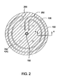
- Figure 2 is a horizontal sectional view of the heated substrate support of Figure 1 ;
- FIG. 3 vertical partial sectional view of another embodiment of a heated substrate support suitable for use with high temperature processing environments
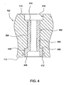
- Figure 4 is a partial sectional view of the heated substrate support taken along section line 4--4 of Figure 2 ;
- Figure 5 is a flow diagram of one embodiment of a method 500 of fabricating a heated substrate support.
- Figure 1 depicts one embodiment of heated aluminum substrate support 100 suitable for use at high temperatures in a semiconductor processing system (not shown).
- a semiconductor processing system that may be adapted to utilize the invention is a CENTURA ® CVD processing system, available from Applied Materials, Inc., located in Santa Clara, California. It is contemplated that the heated aluminum substrate support 100 of the present invention may be utilized in other processing systems, including those available from other manufacturers.
- the heated aluminum substrate support 100 includes a disk-like body 102, a stem 104 and a heating element 106.
- the stem 104 is generally tubular member having a first end 132 that is coupled to the body 102 and an opposing second end 134.
- the stem 104 includes a mounting flange 136 disposed at the first end 132 for coupling the stem 104 to a bottom surface 112 the body 102, as further discussed below.
- the stem 104 also includes an upper main shaft 138 and a lower main shaft 140.
- the upper main shaft 138 has a diameter greater than the lower main shaft 140.
- the lower main shaft 140 includes an annular rib 142 that extends outward to approximately the diameter of the upper main shaft 138.
- Two ceramic heater tubes 130 are disposed within the stem 104.
- the tubes 130 are coupled to an internal flange 144 of the stem 104 disposed proximate the second end 134.
- a conductive rod 146 is disposed through each tube 130 and coupled to respective heater leads 108.
- a connector pin 148 is brazed or otherwise coupled to the conductive rod 146. The pin 148 extends beyond the tube 130 to facilitate coupling power the heating element 106.
- a guide tube 150 is also provided through the stem 104 to facilitate placement of a sensor (not shown) in the body 102.
- the tube 150 extends into a blind hole 152 formed in the bottom surface 112 of the body 102.
- the body 102 is fabricated from aluminum and has an average grain size less than about 250 ⁇ m.
- An average grain size less than about 250 ⁇ m ensures a more uniform dispersion of impurities within the aluminum material comprising the body 102.
- the grain size of the body 102 ensures a more uniform dispersion of impurities by increasing the grain boundary surface area and limiting the size of the point defects caused by the impurities sitting at the grain boundaries.
- the body 102 will have fewer and more dispersed point defects, and correspondingly, fewer and more dispersed initation points for aluminum flouride AlFx film defects comparied to conventional supports, thereby resulting in reduced particle generation and longer support service life.
- An unanticipated benefit of the small grain size is the improved consistancy, repeatablity and quality of an anodic coating covering some embodiments of the body 102.
- the improved unformity and quality of the anodic coating provides improved heater performance.
- the body 102 has an average grain size of less than about 250 ⁇ m may be obtained in a number of ways, of which an examplary is described below. It is contemplated that the average grain size of less than about 250 ⁇ m may be obtained in other ways that benefit from the invention. In embodiments wherein the body 102 is forged, the forgings may be graded by grain size such that only bodies having an average grain size less than about 250 ⁇ m are selected for further fabrication into the aluminum substrate support 100.
- the body 102 is casted in a manner that yields an average grain size of less than about 250 ⁇ m.
- the body 102 may be casted from substantially pure aluminum having an appropriate amount of a grain enhancer added to obtain the desired grain size.
- the grain enhancer is titanium (Ti). In one embodiment, between about 0.03 to about 0.1 weight percent of grain enhancer, such as titanium (Ti), may be utilized to produce an average grain size less than about 250 ⁇ m.
- the heating element 106 is disposed in, embedded or otherwise coupled to the body 102.
- the heating element 106 may be a resistive heater, a conduit for circulating a heat transfer fluid or other suitable heat generator.
- the heating element 106 is capable of elevating the temperature of the body 102 to about 480 degrees Celsius.
- the heating element 106 is a resistive heater having leads 108 extending from the bottom surface 112 of the body 102.
- the leads 108 exit the body 102 in a region circumscribed by the stem 104 and are routed though the stem 104 to facilitate coupling the heating element 106 to a power source for powering the heater.
- the heating element 106 is positioned in the center of the body 102, i.e ., substantially equidistant from the bottom surface 112 and an opposing top surface 114 of the body 102. It is contemplated that the heating element 106 may be positioned in other orientations.
- the heating element 106 is generally arranged in a double loop 202 routed radially outward of lift pin holes 204.
- a mid-point 206 of the heating element 106 is generally positioned substantially equidistant from two adjacent lift pin holes 204.
- the heating element 106 may be casted in place, embedded within a groove or disposed in the body 102 in another fashion.
- Figure 3 depicts a partial sectional view of a body 302 having the heating element 106 embedded within a groove 304.
- the body 302 is substantially similar to the body 102 described above.
- the groove 304 may be formed in the body 302 during the casting, forging or other body forming process. Alternatively, the groove 304 may be machined or otherwise formed in the body 302 after the blank of the body 302 is fabricated.
- the body 302 is fabricated from a cold-worked aluminum stock plate, such as 6061- T651 wrought tooling plate, and has the groove 304 machined therein.
- the heating element 106 is disposed in the groove 304, in one example, by 6061- T651 wrought tooling plate, and has the groove 304 machined therein.
- the groove 304 may be sized accommodate the heating element 106 therein, and in one embodiment, the groove 304 may be sized such that the heating element 106 is press-fit or closely fit into the groove 304.
- a cap 306 closes the groove 304 to capture the heating element 106 therein.
- the cap 306 may be welded to the body 302 using any suitable technique that produces a leak-tight joint between the body 302 and cap 306, such as an electron beam weld.
- the cap 306 and groove 304 geometry allows for the electron beam weld to fully penetrate into body material below the cap 306 to change the stress application point to an orientation perpendicular to the vertical orientation of the weld which greatly reduces leak potential.
- the weld between the body 302 to the stem 104 is also depicted in Figure 3 .
- the body 102 and the stem 104 depicted in Figure 1 may be similarly coupled.
- the body 302 includes a recess 308 configured to accept a mounting flange 136 formed at the first end 132 of the stem 104.
- the mounting flange 136 includes an angled wall 312 that flares outward from the upper main shaft 138 of the stem 104 to an outer flange wall 314.
- the outer flange wall 314 is generally circular in form and includes a lip 316 extending radially outward from an end of the flange wall 314 opposite the angled wall 312.
- the lip 316 is dimensioned to fit closely to and/or press-fit into the sidewalls 310 of the recess 308.
- the exposed end of the weld 322 is not machined after welding.
- the weld 322 also fully penetrates through the lip 316 to the stem 104 and bottom 318 of the body recess 308 (as shown by phantom line 320), which results in the stress application point 324 of the weld 322 to be located at the side of the weld 322 along the plane of the first end 132 of the stem 104.
- the lip 316 becomes a sacrificial backing to form the weld root in material homogenous to the stem 104, thus eliminating the formation of a crack tip which can shorten life expectancy of the substrate support 302.
- the positioning of the stress application point 324 to the side of the weld 322 greatly increases the life cycle of the weld 322.
- the substrate support of the present invention may be utilized in applications having a temperature in excess of 400 and up to 480 degrees Celsius, the resistance of the weld 322 to failure due to the angular offset, in this case about 90 degrees, between the plane of the weld 322 and the stress application point, provides a substantial improvement over conventional butt jointed designs.
- the body 102 of the substrate support 100 generally includes a blind hole 160 formed in the center of the upper surface 114 of the body 102.
- the hole 160 is utilized for locating a ceramic cover plate (not shown) upon which a substrate will rest during processing. It ensures good thermal contact between the ceramic cover plate and the body 102, as the upper surface 114 is roughened, for example, between 46 ⁇ in and 62 ⁇ in RMS.
- FIG 4 is a partial sectional view of the substrate support 100 taken along section line 4--4 of Figure 2 to illustrate a lift pin guide 402 disposed in the lift pin holes 204 of the body 102.
- the guide 402 has a tubular ceramic body 404 having a shoulder 406 formed near a lower end 408.
- the shoulder 406 is faced against a ledge 410 formed in the lift pin holes 204.
- An annular tab 412 formed in the bottom surface 112 of the body 102 is pressed radially inward against the lower end 408 of the guide 402 to lock the guide 402 within the lift pin hole 204.
- An upper surface 414 of the guide 402 is generally recessed from the upper surface 114 of the body 102.
- a counter bore 416, concentric with the lift pin holes 204, is provided in the upper surface 114 of the body 102 to accommodate the distal end of the lift pin (not shown) when recessed below the surface 114.
- the fine grain substrate supports described above have demonstrated excellent aluminum fluoride film performance and extended service life as compared to conventional large grain supports, particularly at process temperatures ranging upward of 400 to 480 degrees Celsius, which is well in excess of recommended aluminum operational temperatures.
- a substrate support having an average grain size of about 500 ⁇ m exhibited a fair amount of aluminum fluoride film defects (and consequently, unacceptable particle generation) after about 21,000 wafer process cycles while a substrate support having an average grain size of about 180 ⁇ m exhibited almost no aluminum fluoride film defects after about 335,000 wafer process cycles.
- Figure 5 is a flow diagram of one embodiment of a method 500 of fabricating a heated substrate support.
- the method 500 begins at step 502 by forming an aluminum body having an average grain size of about 250 ⁇ m.
- forming step 502 may include casting the body with a grain enhancer.
- a titanium or other suitable grain enhancer may be utilized. In one embodiment, between about 0.03 to about 0.1 weight percent of a titanium grain enhancer is utilized.
- forming step 502 may include grading aluminum bodies to select only bodies having an average grain size of about 250 ⁇ m are selected for further fabrication.
- the bodies may be fabricated by forging, casting or other method.
- the formed body is a rolled aluminum plate.
- the forming step includes heating element is installed in the body.
- the heating element is cast in plate.
- the heating element is disposed in a groove formed in the body. The groove may be capped using an electron beam weld or other suitable method.
- the stem is welded to the body.
- the stem is welded to the body using a lap joint that fully penetrates the stem and body so that the stress application point to the weld is substantially perpendicular to the vertical orientation of the weld.
- the body and/or stem and/or selected surfaces thereof may be textured.
- the upper surface of the body is textured.
- selected portions of the body may be coated.
- the body is anodized while the stem is masked so that it remains a bare aluminum surface.
- the body and stem are seasoned with a layer of aluminum fluoride (AlFx).
- an aluminum heated substrate support and method for manufacturing the same has been provided that allows for improved processing of substrates in hot processing environments.
- the fine grain structure of the substrate support body ensures a more uniform dispersion of impurities by increasing the grain boundary surface area and limiting the size of the point defects caused by the impurities sitting at the grain boundaries, resulting in fewer defeat points from which aluminum fluoride film failure or particle generation may be initiated.
- the fine grain body results in excellent anodic coating and robust heater performance, which is advantageously repeatable substrate support to substrate support.
- the fine grain structured substrate support provides superior aluminum fluoride film performance and correspondingly extended service life over conventional designs.
- the improved weld joint between the stem and body of the present invention reduces the probability of weld failure over conventional designs, thereby further extending the service life of the inventive substrate support.
- the invention is also directed to an apparatus for carrying out the disclosed methods and including apparatus parts for performing each described method steps. These method steps may be performed by way of hardware components, a computer programmed by appropriate software, by any combination of the two or in any other manner. Furthermore, the invention is also directed to methods by which the described apparatus operates. It includes method steps for carrying out every function of the apparatus.
Landscapes
- Chemical & Material Sciences (AREA)
- General Chemical & Material Sciences (AREA)
- Chemical Kinetics & Catalysis (AREA)
- Engineering & Computer Science (AREA)
- Materials Engineering (AREA)
- Mechanical Engineering (AREA)
- Metallurgy (AREA)
- Organic Chemistry (AREA)
- Container, Conveyance, Adherence, Positioning, Of Wafer (AREA)
- Resistance Heating (AREA)
- Chemical Vapour Deposition (AREA)
Abstract
Description
- The invention generally relates to a substrate support for use in semiconductor processing, and more specifically to an aluminum substrate support suitable for use in high temperature semiconductor processing systems.
- Integrated circuits have evolved into complex devices that can include millions of transistors, capacitors and resistors on a single chip. The evolution of chip designs continually requires faster circuitry and greater circuit density that demand increasingly precise fabrication processes. One fabrication process frequently used is chemical vapor deposition (CVD).
- Chemical vapor deposition is generally employed to deposit a thin film on a substrate, such as a semiconductor wafer. Chemical vapor deposition is generally accomplished by introducing a precursor gas in to a vacuum chamber. The precursor gas is typically directed through a showerhead situated near the top of the chamber. The precursor gas reacts to form a layer of material on a surface of the substrate that is positioned on a heated substrate support. Purge gas is routed through holes in the support to the edge of the substrate to prevent deposition at the substrate's edge that may cause the substrate to adhere to the support or flake off during processing. Volatile by-products produced during the reaction are pumped from the chamber through an exhaust system.
- One material frequently formed on substrates using a chemical vapor deposition process is tungsten. A precursor gas that may be used to form tungsten generally includes tungsten hexafluoride (WF6) and silane. As the silane and tungsten hexafluoride mix, some "stray" tungsten (i.e., tungsten that does not deposit on the substrate) deposits on the showerhead and other chamber components. The stray tungsten film builds on the showerhead and may become a source of contamination in the chamber. Eventually, the stray tungsten may clog the holes in the showerhead that facilitate the passage of the precursor gas therethrough necessitating the showerhead be removed and cleaned or replaced. Chemical vapor deposition chambers also often require periodic cleaning after depositing other materials, for example dielectric materials such as SiO2.
- To extend the interval in time between the routine maintenance of the showerhead, fluorine based chemistries are generally used to clean (i.e., etch away) the stray tungsten film. The fluorine base chemistry also reacts to form a layer of aluminum fluoride (AlFx) on the heated support that is commonly made of aluminum. The aluminum fluoride (AlFx) layer, if present in a controlled and uniform state, provides a protective coating and sacrificial layer over the heated support. However, if the aluminum fluoride (AlFx) growth becomes random or excessive between different areas of the heated support, the AlFx layer can become defect ridden, and/or form selectively at initiation sites that generate flakes and particles, thus detrimentally becoming a particle generation and contamination source.
- Many conventional aluminum substrate supports are forgings or castings. Forging processes are difficult to control and, as such, forged substrate supports generally exhibit a wide range of material properties, such as a wide range of grain sizes. Casting processes can also exhibit control difficulties which can result in a wide range of material properties, such as a wide range of grain sizes. The inventors have discovered that forged and cast substrate supports exhibiting large grain sizes have poor aluminum fluoride (AlFx) performance, i.e., the aluminum fluoride (AlFx) film has large amounts of defects, high particle generation and, consequently, short service life. Thus, it would be beneficial to produce an aluminum heated substrate support having an advantageous grain size distribution that does enhance the performance of adhered aluminum fluoride (AIFx) films.
- Moreover, the heater body and stem joint of the substrate support must be configured to enable the use of such heaters at high temperatures. As the substrate support may be utilized at process temperatures ranging upward of 400 to 480 degrees Celsius, which is well in excess of recommended aluminum operational temperatures. Weld cracking may promote failure of the adhered aluminum fluoride (AlFx) films, along with vacuum leakage problems.
- Therefore, there is a need in the art for an improved heated support suitable for use in chemical vapor deposition processes.
- The aforementioned problems are at least partly solved by a substrate support as laid out in claim 1, a substrate support as laid out in claim 8 and a method as laid out in claim 11. Further aspects, details, features and embodiments are evident from the dependent claims, the description and the accompanying drawings.
- An aluminum heated substrate support suitable for use in high temperature substrate processing systems and method for fabricating the same are provided. In some embodiments, an aluminum heated substrate support can include an aluminum body, a heating element embedded in the body and a stem coupled to the body. The aluminum body has an average grain size less than about 250 µm. The stem is coupled to a bottom of the body using a fully penetrated lap weld joint.
- In some other embodiments, an aluminum heated substrate support can include a cast aluminum body having an embedded heating element. The cast aluminum body includes a grain enhancer that produces an average grain size less than about 250 µm. In certain embodiments, the grain enhancer is titanium (Ti). In one embodiment, between about 0.03 to about 0.1 weight percent of grain enhancer is utilized to produce an average grain size less than about 250 µm. A stem may be coupled to a bottom of the body using a fully penetrated lap weld joint.
- In some other embodiments, an aluminum heated substrate support can include an aluminum body fabricated from rolled wrought plate stock having an average grain size less than about 250 µm. The body has a mechanically embedded heating element disposed therein.
- The accompanying drawings relate to embodiments of the invention and are described in the following:
-
Figure 1 is a vertical sectional view of one embodiment of a heated substrate support suitable for use with high temperature processing environments; -
Figure 2 is a horizontal sectional view of the heated substrate support ofFigure 1 ; -
Figure 3 vertical partial sectional view of another embodiment of a heated substrate support suitable for use with high temperature processing environments; -
Figure 4 is a partial sectional view of the heated substrate support taken alongsection line 4--4 ofFigure 2 ; and -
Figure 5 is a flow diagram of one embodiment of amethod 500 of fabricating a heated substrate support. - It is to be noted, however, that the appended drawings illustrate only typical embodiments of this invention and are therefore not to be considered limiting of its scope, for the invention may admit to other equally effective embodiments. It is also contemplated that features of one embodiment may be beneficially utilized in other embodiments without further recitation.
-
Figure 1 depicts one embodiment of heated aluminum substrate support 100 suitable for use at high temperatures in a semiconductor processing system (not shown). One suitable semiconductor processing system that may be adapted to utilize the invention is a CENTURA® CVD processing system, available from Applied Materials, Inc., located in Santa Clara, California. It is contemplated that the heated aluminum substrate support 100 of the present invention may be utilized in other processing systems, including those available from other manufacturers. - The heated
aluminum substrate support 100 includes a disk-like body 102, astem 104 and aheating element 106. Thestem 104 is generally tubular member having afirst end 132 that is coupled to thebody 102 and an opposingsecond end 134. Thestem 104 includes amounting flange 136 disposed at thefirst end 132 for coupling thestem 104 to abottom surface 112 thebody 102, as further discussed below. Thestem 104 also includes an uppermain shaft 138 and a lowermain shaft 140. The uppermain shaft 138 has a diameter greater than the lowermain shaft 140. The lowermain shaft 140 includes anannular rib 142 that extends outward to approximately the diameter of the uppermain shaft 138. - Two
ceramic heater tubes 130 are disposed within thestem 104. Thetubes 130 are coupled to aninternal flange 144 of thestem 104 disposed proximate thesecond end 134. Aconductive rod 146 is disposed through eachtube 130 and coupled to respective heater leads 108. Aconnector pin 148 is brazed or otherwise coupled to theconductive rod 146. Thepin 148 extends beyond thetube 130 to facilitate coupling power theheating element 106. - A
guide tube 150 is also provided through thestem 104 to facilitate placement of a sensor (not shown) in thebody 102. In the embodiment depicted inFigure 1 , thetube 150 extends into ablind hole 152 formed in thebottom surface 112 of thebody 102. - The
body 102 is fabricated from aluminum and has an average grain size less than about 250 µm. An average grain size less than about 250 µm ensures a more uniform dispersion of impurities within the aluminum material comprising thebody 102. The grain size of thebody 102 ensures a more uniform dispersion of impurities by increasing the grain boundary surface area and limiting the size of the point defects caused by the impurities sitting at the grain boundaries. Thus, thebody 102 will have fewer and more dispersed point defects, and correspondingly, fewer and more dispersed initation points for aluminum flouride AlFx film defects comparied to conventional supports, thereby resulting in reduced particle generation and longer support service life. An unanticipated benefit of the small grain size is the improved consistancy, repeatablity and quality of an anodic coating covering some embodiments of thebody 102. The improved unformity and quality of the anodic coating provides improved heater performance. - The
body 102 has an average grain size of less than about 250 µm may be obtained in a number of ways, of which an examplary is described below. It is contemplated that the average grain size of less than about 250 µm may be obtained in other ways that benefit from the invention. In embodiments wherein thebody 102 is forged, the forgings may be graded by grain size such that only bodies having an average grain size less than about 250 µm are selected for further fabrication into thealuminum substrate support 100. - In some embodiments, the
body 102 is casted in a manner that yields an average grain size of less than about 250 µm. Thebody 102 may be casted from substantially pure aluminum having an appropriate amount of a grain enhancer added to obtain the desired grain size. In certain embodiments, the grain enhancer is titanium (Ti). In one embodiment, between about 0.03 to about 0.1 weight percent of grain enhancer, such as titanium (Ti), may be utilized to produce an average grain size less than about 250 µm. - The
heating element 106 is disposed in, embedded or otherwise coupled to thebody 102. Theheating element 106 may be a resistive heater, a conduit for circulating a heat transfer fluid or other suitable heat generator. In some embodiments, theheating element 106 is capable of elevating the temperature of thebody 102 to about 480 degrees Celsius. - In one embodiment, the
heating element 106 is a resistiveheater having leads 108 extending from thebottom surface 112 of thebody 102. The leads 108 exit thebody 102 in a region circumscribed by thestem 104 and are routed though thestem 104 to facilitate coupling theheating element 106 to a power source for powering the heater. - In the embodiment depicted in
Figure 1 , theheating element 106 is positioned in the center of thebody 102, i.e., substantially equidistant from thebottom surface 112 and an opposingtop surface 114 of thebody 102. It is contemplated that theheating element 106 may be positioned in other orientations. - Referring to the sectional view of the
body 102 depicted inFigure 2 , theheating element 106 is generally arranged in adouble loop 202 routed radially outward of lift pin holes 204. A mid-point 206 of theheating element 106 is generally positioned substantially equidistant from two adjacent lift pin holes 204. Theheating element 106 may be casted in place, embedded within a groove or disposed in thebody 102 in another fashion. -
Figure 3 depicts a partial sectional view of abody 302 having theheating element 106 embedded within agroove 304. Thebody 302 is substantially similar to thebody 102 described above. Thegroove 304 may be formed in thebody 302 during the casting, forging or other body forming process. Alternatively, thegroove 304 may be machined or otherwise formed in thebody 302 after the blank of thebody 302 is fabricated. - In the embodiment depicted in
Figure 3 , thebody 302 is fabricated from a cold-worked aluminum stock plate, such as 6061- T651 wrought tooling plate, and has thegroove 304 machined therein. Theheating element 106 is disposed in thegroove 304, in one example, by 6061- T651 wrought tooling plate, and has thegroove 304 machined therein. Thegroove 304 may be sized accommodate theheating element 106 therein, and in one embodiment, thegroove 304 may be sized such that theheating element 106 is press-fit or closely fit into thegroove 304. - A
cap 306 closes thegroove 304 to capture theheating element 106 therein. Thecap 306 may be welded to thebody 302 using any suitable technique that produces a leak-tight joint between thebody 302 andcap 306, such as an electron beam weld. Thecap 306 and groove 304 geometry allows for the electron beam weld to fully penetrate into body material below thecap 306 to change the stress application point to an orientation perpendicular to the vertical orientation of the weld which greatly reduces leak potential. - The weld between the
body 302 to thestem 104 is also depicted inFigure 3 . Thebody 102 and thestem 104 depicted inFigure 1 may be similarly coupled. Thebody 302 includes arecess 308 configured to accept a mountingflange 136 formed at thefirst end 132 of thestem 104. - The mounting
flange 136 includes anangled wall 312 that flares outward from the uppermain shaft 138 of thestem 104 to anouter flange wall 314. Theouter flange wall 314 is generally circular in form and includes alip 316 extending radially outward from an end of theflange wall 314 opposite theangled wall 312. Thelip 316 is dimensioned to fit closely to and/or press-fit into thesidewalls 310 of therecess 308. Aweld 322, shown here as a lap joint, fills the gap defined between thesidewalls 310 of therecess 308 and theflange wall 314 of thestem 104. The exposed end of theweld 322 is not machined after welding. Theweld 322 also fully penetrates through thelip 316 to thestem 104 andbottom 318 of the body recess 308 (as shown by phantom line 320), which results in thestress application point 324 of theweld 322 to be located at the side of theweld 322 along the plane of thefirst end 132 of thestem 104. Thus, thelip 316 becomes a sacrificial backing to form the weld root in material homogenous to thestem 104, thus eliminating the formation of a crack tip which can shorten life expectancy of thesubstrate support 302. The positioning of thestress application point 324 to the side of theweld 322 greatly increases the life cycle of theweld 322. As the substrate support of the present invention may be utilized in applications having a temperature in excess of 400 and up to 480 degrees Celsius, the resistance of theweld 322 to failure due to the angular offset, in this case about 90 degrees, between the plane of theweld 322 and the stress application point, provides a substantial improvement over conventional butt jointed designs. - Returning to
Figure 1 , thebody 102 of thesubstrate support 100 generally includes ablind hole 160 formed in the center of theupper surface 114 of thebody 102. Thehole 160 is utilized for locating a ceramic cover plate (not shown) upon which a substrate will rest during processing. It ensures good thermal contact between the ceramic cover plate and thebody 102, as theupper surface 114 is roughened, for example, between 46 µin and 62 µin RMS. -
Figure 4 is a partial sectional view of thesubstrate support 100 taken alongsection line 4--4 ofFigure 2 to illustrate alift pin guide 402 disposed in the lift pin holes 204 of thebody 102. Theguide 402 has a tubularceramic body 404 having ashoulder 406 formed near alower end 408. Theshoulder 406 is faced against aledge 410 formed in the lift pin holes 204. Anannular tab 412 formed in thebottom surface 112 of thebody 102 is pressed radially inward against thelower end 408 of theguide 402 to lock theguide 402 within thelift pin hole 204. Anupper surface 414 of theguide 402 is generally recessed from theupper surface 114 of thebody 102. A counter bore 416, concentric with the lift pin holes 204, is provided in theupper surface 114 of thebody 102 to accommodate the distal end of the lift pin (not shown) when recessed below thesurface 114. - The fine grain substrate supports described above have demonstrated excellent aluminum fluoride film performance and extended service life as compared to conventional large grain supports, particularly at process temperatures ranging upward of 400 to 480 degrees Celsius, which is well in excess of recommended aluminum operational temperatures. For example, a substrate support having an average grain size of about 500 µm exhibited a fair amount of aluminum fluoride film defects (and consequently, unacceptable particle generation) after about 21,000 wafer process cycles while a substrate support having an average grain size of about 180 µm exhibited almost no aluminum fluoride film defects after about 335,000 wafer process cycles.
-
Figure 5 is a flow diagram of one embodiment of amethod 500 of fabricating a heated substrate support. Themethod 500 begins atstep 502 by forming an aluminum body having an average grain size of about 250 µm. - In one embodiment, forming
step 502 may include casting the body with a grain enhancer. A titanium or other suitable grain enhancer may be utilized. In one embodiment, between about 0.03 to about 0.1 weight percent of a titanium grain enhancer is utilized. - In another embodiment, forming
step 502 may include grading aluminum bodies to select only bodies having an average grain size of about 250 µm are selected for further fabrication. The bodies may be fabricated by forging, casting or other method. In one embodiment, the formed body is a rolled aluminum plate. - The forming step includes heating element is installed in the body. In some embodiments wherein the body is casted, the heating element is cast in plate. In other embodiments wherein the body is casted, forged or a rolled aluminum plate, the heating element is disposed in a groove formed in the body. The groove may be capped using an electron beam weld or other suitable method.
- At
step 504, the stem is welded to the body. In one embodiment, the stem is welded to the body using a lap joint that fully penetrates the stem and body so that the stress application point to the weld is substantially perpendicular to the vertical orientation of the weld. - At an
optional step 506, the body and/or stem and/or selected surfaces thereof may be textured. In one embodiment, the upper surface of the body is textured. - At an
optional step 508, selected portions of the body may be coated. In one embodiment, the body is anodized while the stem is masked so that it remains a bare aluminum surface. In another embodiment, the body and stem are seasoned with a layer of aluminum fluoride (AlFx). - Thus, an aluminum heated substrate support and method for manufacturing the same has been provided that allows for improved processing of substrates in hot processing environments. The fine grain structure of the substrate support body ensures a more uniform dispersion of impurities by increasing the grain boundary surface area and limiting the size of the point defects caused by the impurities sitting at the grain boundaries, resulting in fewer defeat points from which aluminum fluoride film failure or particle generation may be initiated. Additionally, the fine grain body results in excellent anodic coating and robust heater performance, which is advantageously repeatable substrate support to substrate support. Thus, the fine grain structured substrate support provides superior aluminum fluoride film performance and correspondingly extended service life over conventional designs. Moreover, the improved weld joint between the stem and body of the present invention reduces the probability of weld failure over conventional designs, thereby further extending the service life of the inventive substrate support.
- While the foregoing is directed to some embodiments of the present invention, other and further embodiments of the invention may be devised without departing from the basic scope thereof, and the scope thereof is determined by the claims that follow.
- The invention is also directed to an apparatus for carrying out the disclosed methods and including apparatus parts for performing each described method steps. These method steps may be performed by way of hardware components, a computer programmed by appropriate software, by any combination of the two or in any other manner. Furthermore, the invention is also directed to methods by which the described apparatus operates. It includes method steps for carrying out every function of the apparatus.
Claims (18)
- A substrate support suitable for use in a semiconductor processing system, the substrate support comprising:an aluminum body having an average grain size less than about 250 µm;a heating element embedded in the body; anda stem coupled to a bottom of the body by a fully penetrated lap weld joint.
- The substrate support of claim 1 wherein the heating element further comprises:leads extending into the stem.
- The substrate support of claim 1 further comprising:a ceramic guide disposed in a lift pin hole formed through the body.
- The substrate support of claim 1, where the body further comprises:a grain enhancer.
- The substrate support of claim 1, where the body further comprises:a titanium grain enhancer.
- The substrate support of claim 1, where the body further comprises:between about 0.03 to about 0.1 weight percent of a titanium grain enhancer.
- The substrate support of claim 1, where the body is cast or forged
- A substrate support suitable for use in a semiconductor processing system, the substrate support comprising:a rolled aluminum body having an average grain size less than about 250 µm; anda heating element disposed in the body.
- The substrate support of claim 8, where the body further comprises:a 6061- T651 wrought tooling plate having a groove machined therein, wherein the heating element is disposed in the groove.
- The substrate support of claim 8, further comprising:a stem coupled to a bottom of the body by a fully penetrated lap weld joint.
- A method for fabricating a substrate support suitable for using in high temperature substrate processing environments, the method comprising:selecting an aluminum body having an average grain size less than about 250 µm, the body having a top surface having a center blind hole and an opposing bottom surface; andlap welding a tubular stem into a recess formed in the bottom surface of the body, wherein a lip of the stem forms a sacrificial backing to form a weld root, and wherein leads of a heating element disposed in the body extend into the tube.
- The method of claim 11, wherein the selecting further comprises:selecting a forged body having an average grain size less than about 250 µm from a plurality of forged bodies including bodies having an average grain size greater than about 250 µm.
- The method of claim 11 further comprising:casting the body.
- The method of claim 13, wherein casting further comprises:casting the body from an aluminum material containing a grain enhancer.
- The method of claim 13, wherein casting further comprises:casting the body from an aluminum material containing a titanium grain enhancer.
- The method of claim 13, wherein casting further comprisies:casting the body from an aluminum material containing between about 0.03 to about 0.1 weight percent of a titanium grain enhancer.
- The method of claim 11 further comprising:forming a groove configured to accept the heating element in a rolled aluminum plate to form the body.
- The method of claim 11 further comprising:forming a groove configured to accept the heating element in a 6061-T651 wrought aluminum tooling plate to form the body.
Applications Claiming Priority (2)
| Application Number | Priority Date | Filing Date | Title |
|---|---|---|---|
| US88561207P | 2007-01-18 | 2007-01-18 | |
| US88562207P | 2007-01-18 | 2007-01-18 |
Publications (2)
| Publication Number | Publication Date |
|---|---|
| EP1947689A2 true EP1947689A2 (en) | 2008-07-23 |
| EP1947689A3 EP1947689A3 (en) | 2011-03-30 |
Family
ID=39183077
Family Applications (1)
| Application Number | Title | Priority Date | Filing Date |
|---|---|---|---|
| EP08000957A Withdrawn EP1947689A3 (en) | 2007-01-18 | 2008-01-18 | High temperature fine grain aluminium heater |
Country Status (5)
| Country | Link |
|---|---|
| EP (1) | EP1947689A3 (en) |
| JP (1) | JP5544061B2 (en) |
| KR (1) | KR101059060B1 (en) |
| SG (1) | SG144830A1 (en) |
| TW (1) | TWI478214B (en) |
Families Citing this family (2)
| Publication number | Priority date | Publication date | Assignee | Title |
|---|---|---|---|---|
| KR102278081B1 (en) * | 2019-06-27 | 2021-07-19 | 세메스 주식회사 | Apparatus and Method for treating substrate |
| WO2021247627A1 (en) * | 2020-06-03 | 2021-12-09 | Lam Research Corporation | Monobloc pedestal for efficient heat transfer |
Family Cites Families (9)
| Publication number | Priority date | Publication date | Assignee | Title |
|---|---|---|---|---|
| JPH06326081A (en) * | 1993-05-17 | 1994-11-25 | Fuji Electric Co Ltd | Heating device for dry thin film processing equipment |
| JP3746878B2 (en) * | 1997-07-23 | 2006-02-15 | 株式会社神戸製鋼所 | Al alloy for semiconductor manufacturing equipment with excellent gas corrosion resistance and plasma corrosion resistance, and excellent heat resistance for aluminum manufacturing equipment and materials for semiconductor manufacturing equipment |
| JP4627392B2 (en) * | 2001-09-26 | 2011-02-09 | 株式会社アルバック | Vacuum processing apparatus and vacuum processing method |
| US7048814B2 (en) * | 2002-02-08 | 2006-05-23 | Applied Materials, Inc. | Halogen-resistant, anodized aluminum for use in semiconductor processing apparatus |
| JP4010170B2 (en) * | 2002-04-11 | 2007-11-21 | ソニー株式会社 | Method for manufacturing photoelectric conversion element |
| JP4008401B2 (en) * | 2003-09-22 | 2007-11-14 | 日本碍子株式会社 | Manufacturing method of substrate mounting table |
| JP2005109169A (en) * | 2003-09-30 | 2005-04-21 | Ngk Insulators Ltd | Substrate heating apparatus and manufacturing method thereof |
| JP4133958B2 (en) * | 2004-08-04 | 2008-08-13 | 日本発条株式会社 | Apparatus for heating or cooling a workpiece and method for manufacturing the same |
| US20060075970A1 (en) * | 2004-10-13 | 2006-04-13 | Guenther Rolf A | Heated substrate support and method of fabricating same |
-
2008
- 2008-01-11 SG SG200800277-6A patent/SG144830A1/en unknown
- 2008-01-15 TW TW097101540A patent/TWI478214B/en active
- 2008-01-16 JP JP2008006487A patent/JP5544061B2/en active Active
- 2008-01-18 EP EP08000957A patent/EP1947689A3/en not_active Withdrawn
- 2008-01-18 KR KR1020080005778A patent/KR101059060B1/en active Active
Also Published As
| Publication number | Publication date |
|---|---|
| EP1947689A3 (en) | 2011-03-30 |
| KR101059060B1 (en) | 2011-08-24 |
| SG144830A1 (en) | 2008-08-28 |
| TWI478214B (en) | 2015-03-21 |
| JP2008177572A (en) | 2008-07-31 |
| KR20080068592A (en) | 2008-07-23 |
| JP5544061B2 (en) | 2014-07-09 |
| TW200903593A (en) | 2009-01-16 |
Similar Documents
| Publication | Publication Date | Title |
|---|---|---|
| JP6909034B2 (en) | Baffle plate and shower head assembly and corresponding manufacturing method | |
| US20030148035A1 (en) | Article for use in a semiconductor processing chamber and method of fabricating same | |
| US6761771B2 (en) | Semiconductor substrate-supporting apparatus | |
| KR100296533B1 (en) | Tungsten nucleation method during tungsten CVD process performed by WF6 reduction in vacuum chamber without the use of silane | |
| US8540819B2 (en) | Ceramic heater | |
| US7674726B2 (en) | Parts for deposition reactors | |
| US9917001B2 (en) | High temperature fine grain aluminum heater | |
| EP1081744A2 (en) | Method and apparatus for preventing edge deposition | |
| US6383302B2 (en) | Apparatus and method for manufacturing semiconductor device | |
| JP4815724B2 (en) | Shower head structure and film forming apparatus | |
| JPH1074705A (en) | High temperature susceptor | |
| US20220336192A1 (en) | Metal component and manufacturing method thereof and process chamber having the metal component | |
| KR20210153149A (en) | electrostatic chuck system | |
| US20170137924A1 (en) | Interior material for thin film deposition device and method for manufacturing same | |
| WO2021257225A1 (en) | High temperature face plate for deposition application | |
| EP1947689A2 (en) | High temperature fine grain aluminium heater | |
| US20060182886A1 (en) | Method and system for improved delivery of a precursor vapor to a processing zone | |
| JP3170248B2 (en) | Semiconductor substrate holding device | |
| CN101230451A (en) | High temperature fine particle aluminum heater | |
| TWI518819B (en) | Extended chamber liner to improve the average time between process chamber cleaning | |
| JP2008270400A (en) | Wafer holder for semiconductor manufacturing apparatus and semiconductor manufacturing apparatus equipped with the same | |
| US12125734B2 (en) | Vacuum seal for electrostatic chuck | |
| US10727092B2 (en) | Heated substrate support ring | |
| US20250313933A1 (en) | Method for operating film forming device and film forming device | |
| JP2891991B1 (en) | Plasma CVD equipment |
Legal Events
| Date | Code | Title | Description |
|---|---|---|---|
| PUAI | Public reference made under article 153(3) epc to a published international application that has entered the european phase |
Free format text: ORIGINAL CODE: 0009012 |
|
| AK | Designated contracting states |
Kind code of ref document: A2 Designated state(s): AT BE BG CH CY CZ DE DK EE ES FI FR GB GR HR HU IE IS IT LI LT LU LV MC MT NL NO PL PT RO SE SI SK TR |
|
| AX | Request for extension of the european patent |
Extension state: AL BA MK RS |
|
| PUAL | Search report despatched |
Free format text: ORIGINAL CODE: 0009013 |
|
| AK | Designated contracting states |
Kind code of ref document: A3 Designated state(s): AT BE BG CH CY CZ DE DK EE ES FI FR GB GR HR HU IE IS IT LI LT LU LV MC MT NL NO PL PT RO SE SI SK TR |
|
| AX | Request for extension of the european patent |
Extension state: AL BA MK RS |
|
| RIC1 | Information provided on ipc code assigned before grant |
Ipc: H02N 13/00 20060101ALI20110222BHEP Ipc: C23C 16/458 20060101ALI20110222BHEP Ipc: H01L 21/683 20060101ALI20110222BHEP Ipc: H01L 21/687 20060101AFI20080327BHEP |
|
| AKY | No designation fees paid | ||
| REG | Reference to a national code |
Ref country code: DE Ref legal event code: R108 |
|
| STAA | Information on the status of an ep patent application or granted ep patent |
Free format text: STATUS: THE APPLICATION IS DEEMED TO BE WITHDRAWN |
|
| REG | Reference to a national code |
Ref country code: DE Ref legal event code: R108 Effective date: 20111207 |
|
| 18D | Application deemed to be withdrawn |
Effective date: 20110730 |