EP1947658A1 - Toroidal inductor design for improved Q - Google Patents
Toroidal inductor design for improved Q Download PDFInfo
- Publication number
- EP1947658A1 EP1947658A1 EP08000854A EP08000854A EP1947658A1 EP 1947658 A1 EP1947658 A1 EP 1947658A1 EP 08000854 A EP08000854 A EP 08000854A EP 08000854 A EP08000854 A EP 08000854A EP 1947658 A1 EP1947658 A1 EP 1947658A1
- Authority
- EP
- European Patent Office
- Prior art keywords
- type
- coil
- conductive
- elongated
- segment
- Prior art date
- Legal status (The legal status is an assumption and is not a legal conclusion. Google has not performed a legal analysis and makes no representation as to the accuracy of the status listed.)
- Withdrawn
Links
- 238000013461 design Methods 0.000 title description 5
- 239000004020 conductor Substances 0.000 claims abstract description 75
- 239000000758 substrate Substances 0.000 claims abstract description 70
- 238000000034 method Methods 0.000 claims abstract description 28
- 239000011162 core material Substances 0.000 claims abstract description 9
- 239000000919 ceramic Substances 0.000 description 49
- 239000010410 layer Substances 0.000 description 44
- 239000000463 material Substances 0.000 description 7
- 230000015572 biosynthetic process Effects 0.000 description 4
- 238000004519 manufacturing process Methods 0.000 description 4
- 229920000106 Liquid crystal polymer Polymers 0.000 description 2
- 239000004977 Liquid-crystal polymers (LCPs) Substances 0.000 description 2
- 238000012545 processing Methods 0.000 description 2
- JBRZTFJDHDCESZ-UHFFFAOYSA-N AsGa Chemical compound [As]#[Ga] JBRZTFJDHDCESZ-UHFFFAOYSA-N 0.000 description 1
- 239000004593 Epoxy Substances 0.000 description 1
- 229910002601 GaN Inorganic materials 0.000 description 1
- 229910001218 Gallium arsenide Inorganic materials 0.000 description 1
- JMASRVWKEDWRBT-UHFFFAOYSA-N Gallium nitride Chemical compound [Ga]#N JMASRVWKEDWRBT-UHFFFAOYSA-N 0.000 description 1
- GPXJNWSHGFTCBW-UHFFFAOYSA-N Indium phosphide Chemical compound [In]#P GPXJNWSHGFTCBW-UHFFFAOYSA-N 0.000 description 1
- XUIMIQQOPSSXEZ-UHFFFAOYSA-N Silicon Chemical compound [Si] XUIMIQQOPSSXEZ-UHFFFAOYSA-N 0.000 description 1
- 238000010344 co-firing Methods 0.000 description 1
- 238000007796 conventional method Methods 0.000 description 1
- 230000000694 effects Effects 0.000 description 1
- 229910052732 germanium Inorganic materials 0.000 description 1
- GNPVGFCGXDBREM-UHFFFAOYSA-N germanium atom Chemical compound [Ge] GNPVGFCGXDBREM-UHFFFAOYSA-N 0.000 description 1
- 239000002241 glass-ceramic Substances 0.000 description 1
- 229910052737 gold Inorganic materials 0.000 description 1
- 238000003698 laser cutting Methods 0.000 description 1
- 238000010329 laser etching Methods 0.000 description 1
- 238000003754 machining Methods 0.000 description 1
- 238000003801 milling Methods 0.000 description 1
- 229920001721 polyimide Polymers 0.000 description 1
- 229920006254 polymer film Polymers 0.000 description 1
- 238000012805 post-processing Methods 0.000 description 1
- 238000004080 punching Methods 0.000 description 1
- 238000007650 screen-printing Methods 0.000 description 1
- 239000004065 semiconductor Substances 0.000 description 1
- 229910052710 silicon Inorganic materials 0.000 description 1
- 239000010703 silicon Substances 0.000 description 1
- 229910052709 silver Inorganic materials 0.000 description 1
- 239000002356 single layer Substances 0.000 description 1
- 238000012360 testing method Methods 0.000 description 1
- 238000004804 winding Methods 0.000 description 1
Images




Classifications
-
- H—ELECTRICITY
- H01—ELECTRIC ELEMENTS
- H01F—MAGNETS; INDUCTANCES; TRANSFORMERS; SELECTION OF MATERIALS FOR THEIR MAGNETIC PROPERTIES
- H01F17/00—Fixed inductances of the signal type
- H01F17/0006—Printed inductances
- H01F17/0033—Printed inductances with the coil helically wound around a magnetic core
-
- H—ELECTRICITY
- H01—ELECTRIC ELEMENTS
- H01F—MAGNETS; INDUCTANCES; TRANSFORMERS; SELECTION OF MATERIALS FOR THEIR MAGNETIC PROPERTIES
- H01F17/00—Fixed inductances of the signal type
- H01F17/0006—Printed inductances
- H01F17/0013—Printed inductances with stacked layers
-
- H—ELECTRICITY
- H01—ELECTRIC ELEMENTS
- H01F—MAGNETS; INDUCTANCES; TRANSFORMERS; SELECTION OF MATERIALS FOR THEIR MAGNETIC PROPERTIES
- H01F17/00—Fixed inductances of the signal type
- H01F17/04—Fixed inductances of the signal type with magnetic core
- H01F17/06—Fixed inductances of the signal type with magnetic core with core substantially closed in itself, e.g. toroid
- H01F17/062—Toroidal core with turns of coil around it
-
- H—ELECTRICITY
- H01—ELECTRIC ELEMENTS
- H01F—MAGNETS; INDUCTANCES; TRANSFORMERS; SELECTION OF MATERIALS FOR THEIR MAGNETIC PROPERTIES
- H01F27/00—Details of transformers or inductances, in general
- H01F27/28—Coils; Windings; Conductive connections
- H01F27/2804—Printed windings
- H01F2027/2814—Printed windings with only part of the coil or of the winding in the printed circuit board, e.g. the remaining coil or winding sections can be made of wires or sheets
-
- Y—GENERAL TAGGING OF NEW TECHNOLOGICAL DEVELOPMENTS; GENERAL TAGGING OF CROSS-SECTIONAL TECHNOLOGIES SPANNING OVER SEVERAL SECTIONS OF THE IPC; TECHNICAL SUBJECTS COVERED BY FORMER USPC CROSS-REFERENCE ART COLLECTIONS [XRACs] AND DIGESTS
- Y10—TECHNICAL SUBJECTS COVERED BY FORMER USPC
- Y10T—TECHNICAL SUBJECTS COVERED BY FORMER US CLASSIFICATION
- Y10T29/00—Metal working
- Y10T29/49—Method of mechanical manufacture
- Y10T29/49002—Electrical device making
- Y10T29/4902—Electromagnet, transformer or inductor
-
- Y—GENERAL TAGGING OF NEW TECHNOLOGICAL DEVELOPMENTS; GENERAL TAGGING OF CROSS-SECTIONAL TECHNOLOGIES SPANNING OVER SEVERAL SECTIONS OF THE IPC; TECHNICAL SUBJECTS COVERED BY FORMER USPC CROSS-REFERENCE ART COLLECTIONS [XRACs] AND DIGESTS
- Y10—TECHNICAL SUBJECTS COVERED BY FORMER USPC
- Y10T—TECHNICAL SUBJECTS COVERED BY FORMER US CLASSIFICATION
- Y10T29/00—Metal working
- Y10T29/49—Method of mechanical manufacture
- Y10T29/49002—Electrical device making
- Y10T29/4902—Electromagnet, transformer or inductor
- Y10T29/49073—Electromagnet, transformer or inductor by assembling coil and core
Definitions
- the inventive arrangements relate generally to inductors and more particularly to toroidal inductors.
- Embedded toroidal inductors are known in the art.
- U.S. Patent No. 6,990,729 to Pleskach et al. discloses a method for forming an embedded toroidal inductor. The method includes the step of forming in a ceramic substrate a first plurality of conductive vias radially spaced a first distance from a central axis so as to define an inner circumference.
- a second plurality of conductive vias is formed radially spaced a second distance about the central axis so as to define an outer circumference.
- a first plurality of conductive traces forming an electrical connection between substantially adjacent ones of the first and second plurality of conductive vias is formed on a first surface of the ceramic substrate.
- a second plurality of conductive traces forming an electrical connection between circumferentially offset ones of the first and second plurality of conductive vias is formed on a second surface of the ceramic substrate opposed from the first surface to define a three dimensional toroidal coil.
- DCR direct current resistance
- the invention concerns an inductor and method for forming an inductor.
- the inductor comprises a coil formed from an elongated conductor extending around a core material and defining a plurality of turns.
- the elongated conductor includes one or more coil segments of a first type.
- Each coil segment of the first type is comprised of a plurality of elongated parallel conductors spaced apart and electrically connected by conductive links at predetermined intervals along their respective lengths.
- Each of the elongated parallel conductors is comprised of a conductive trace disposed on a surface of a substrate.
- the conductive links are formed from vias defined in a substrate.
- the inductor is comprised of one or more coil segments of a second type.
- Each coil segment of the second type is formed of a single conductor.
- the single conductor comprising the coil segment of the second type comprises a conductive via formed in a substrate.
- the coil segment of the first type and the coil segment of the second type are arranged in a series configuration to form the elongated conductor.
- the elongated conductor is comprised of a plurality of coil segments of the first type and a plurality of coil segments of the second type.
- Each coil segment of the second type defines a series electrical connection between coil segments of the first type.
- the inductor can include a coil formed from an elongated conductor extending around a core material and defining a plurality of turns.
- the elongated conductor includes a plurality of coil segments arranged in an alternating pattern of a first type segment and a second type segment.
- the first type segment comprises a plurality of parallel conductors spaced apart and electrically connected at predetermined intervals along a length of the plurality of parallel conductors.
- the second type segment comprises a single elongated conductor comprised of conductive vias formed in a substrate.
- the conductive traces are connected at the predetermined intervals by one or more conductive vias.
- the invention can also comprise a method for forming an inductor.
- the method includes forming a coil from an elongated conductor extending around a core material to define a plurality of turns.
- the method also includes the step of forming the elongated conductor to include at least one coil segment of a first type comprised of a plurality of elongated parallel conductors spaced apart.
- the elongated parallel conductors are electrically connected by means of conductive links spaced at predetermined intervals along a length of the plurality of elongated parallel conductors.
- each of the parallel conductors is formed as a conductive trace disposed on a surface of the substrate.
- the conductive links are formed from vias defined in a substrate.
- the method can also include the step of forming the elongated conductor of at least one coil segment of a second type.
- the coil segment of the second type is formed of a single conductor.
- Each coil segment of the second type is formed as a conductive via formed in a substrate.
- one or more coil segments of the first type and one or more coil segments of the second type are arranged in a series configuration to form the elongated conductor.
- the method includes the step of forming with at least one coil segment of the second type a series electrical connection between a plurality of the coil segments of the first type.
- the method can include forming an elongated conductor which extends a plurality of turns around a core material to define a coil.
- the elongated conductor is selected to include a plurality of coil segments arranged in an alternating pattern of a first type segment and a second type segment.
- the first type segment is selected to include a plurality of parallel conductors spaced apart and electrically connected to each other at predetermined intervals along a length of the plurality of parallel conductors.
- the second type segment includes a single conductor.
- the method further comprises forming the second type segments as conductive vias disposed within a substrate.
- each parallel conductor is formed as a conductive trace disposed on a surface of a substrate.
- the conductive traces are connected at the predetermined intervals by one or more conductive vias.
- the invention concerns an improved toroidal inductor integrated within a ceramic substrate and a method of making same.
- the substrate is described herein as a ceramic substrate.
- substrate is described herein as a ceramic substrate.
- substrate is described herein as a ceramic substrate.
- substrate is not limited in this regard.
- Substrates formed of other materials can also be used.
- such materials include, but are not limited to liquid crystal polymer (LCP), polymer film, polyimide film, epoxy laminates, or semiconductor materials such as silicon, gallium arsenide, gallium nitride, germanium or indium phosphide.
- the inductor 100 comprises a coil formed of an elongated conductor defining a plurality of turns and extending around a core material 103.
- the improved toroidal coil structure includes a plurality of coil segments arranged in an alternating pattern.
- the coil segments include a first type coil segment 101 and a second type coil segment 102.
- the first type coil segment 101 is comprised of a plurality of elongated parallel conductors 104, 105.
- a first elongated parallel conductor 104 forms a first parallel conductor pair with a second elongated parallel conductor 105.
- the parallel conductors 104, 105 are spaced apart from each other and electrically connected at locations along their elongated length by at least one first conductive link 108.
- the second type coil segments 102 provide a series electrical connection between spaced apart ones of the first type coil segment 101.
- a first type coil segment 101 is formed of a single conductive trace disposed on a surface of a substrate.
- conductive traces have a relatively low cross sectional area. Accordingly, they tend to have a relatively high resistance.
- this problem is overcome by using a plurality of elongated parallel conductors 104, 105 to decrease the direct current resistance.
- Conventional embedded toroidal inductors do not make use of separate parallel conductors to form a first type coil segment 101.
- conductive links 108 are used to minimize the effect of any capacitance that might otherwise exist as between the elongated parallel conductors 104, 105.
- the second type coil segments 102 can be formed as conductor filled vias using conventional circuit board manufacturing techniques.
- the method can begin with step 202 by forming a suitably sized piece of an unfired ceramic substrate layer 300.
- the ceramic substrate layer 300 can be any of a variety of commercially available glass ceramic substrates designed to be calcined at 800°C to 1,050°C. This class of materials is commonly referred to as low-temperature co-fired ceramics (LTCC). Such LTCC materials have a number of advantages that make them especially useful as substrates for RF systems.
- low temperature 951 co-fire Green TapeTM from Dupont ® is Au and Ag compatible, and it has a thermal coefficient of expansion (TCE) and relative strength that are suitable for many applications.
- TCE thermal coefficient of expansion
- Other similar types of ceramic tapes can also be used.
- the size of the ceramic tape can be determined by a variety of factors depending upon the particular application. For example, if the toroidal inductor is to form part of a larger RF circuit, the ceramic tape can be sized to accommodate the RF circuit in which the toroidal inductor forms a component.
- a first plurality of conductive vias 302 and a via 312 can be formed in the unfired ceramic substrate layer 300.
- This step can be performed using conventional techniques.
- vias can be formed by punching, laser cutting, or etching holes in the unfired ceramic substrate layer 300.
- the first plurality of conductive vias 302 can be radially spaced a first distance d1 from a central axis 401 so as to define an inner circumference of a toroidal inductor.
- a second plurality of conductive vias 304 can be similarly formed radially spaced a second distance d2 about the central axis 401 so as to define an outer circumference.
- the vias can extend substantially between opposing surfaces 306, 408 of the ceramic substrate layer 300.
- Each conductive via 302 can be positioned radially adjacent to a conductive via 304.
- radially adjacent means that two vias that are approximately radially aligned relative to central axis 401 and positioned adjacent to each other.
- Vias 302A and 304A are examples of radially adjacent vias.
- radially adjacent conductive vias are not necessarily precisely aligned radially.
- Such radially adjacent vias can also include vias that are offset circumferentially from one another to some degree.
- vias 302A and 304B represent circumferentially offset vias. As can be seen in FIG. 3 , circumferentially offset vias are not aligned radially.
- the via holes of the first and second pluralities of conductive vias 302, 304 are filled with conductive paste or any other suitable conductive element.
- the process can continue in step 210 by disposing a first plurality of conductive traces 510 on ceramic substrate layer 300.
- the first plurality of conductive traces 510 on surface 306 form electrical connections between respective ones of the first plurality of conductive vias and second plurality of conductive vias that are substantially radially adjacent, as defined earlier.
- additional conductive traces 514 and 516 can also be added to facilitate in the formation of electrical terminals.
- the conductive traces 510 can be formed using conventional PCB methods which are known to the skilled artisan, such as thick film screen printing, photoengraving, and PCB milling.
- a third plurality of conductive vias 803 are formed at predetermined intervals through the second ceramic substrate layer 700.
- the third plurality of vias 803 is located within a predetermined area which corresponds to each of the respective lengths of second conductive traces 710 (discussed below). This concept is best understood by referring to FIG. 8B .
- each trace 710 has the third plurality of vias 803 positioned at locations along the length of the trace 710 and at opposing ends of the trace 710.
- the third plurality of conductive vias 803 are filled with conductive paste or any other suitable conductive element.
- a second plurality of conductive traces 710 is provided on surface 706 of the second substrate layer 700.
- additional conductive trace 717 can also be added to facilitate in the formation of electrical terminals.
- the second plurality of conductive traces 710 is arranged so that when the first and second ceramic substrate layers 300, 700 are aligned and stacked as shown in FIGS. 9 and 10 , the traces 710 on surface 706 will provide an electrical connection between circumferentially offset ones of the first and second pluralities of conductive vias 302, 304.
- a fourth plurality of conductive vias 1203 are formed at predetermined intervals through the third ceramic substrate layer 1100.
- the hole locations are defined within the respective lengths of third conductive traces 1110 (discussed below).
- the fourth plurality of conductive vias 1203 are filled with conductive paste or any other suitable conductive element.
- the third plurality of conductive traces 1110 is provided on surface 1106 of the third substrate layer 1100.
- additional conductive traces 1114, 1116 can also be added to facilitate in the formation of electrical terminals.
- the third plurality of conductive traces 1110 is arranged so that when the ceramic substrate layers 300 and 1100 are aligned and stacked as shown in FIGS. 13 and 14 , the traces 1110 on surface 1106 and the conductive traces 510 on surface 306 define a plurality of elongated parallel conductors.
- the elongated parallel conductors are aligned with each other, spaced apart and electrically connected by conductive links defined by the fourth plurality of conductive vias 1203.
- a fourth ceramic substrate layer 1500 is formed in step 224.
- a fourth plurality of conductive traces 1510 is provided on surface 1506 of the fourth substrate layer 1500.
- the fourth plurality of conductive traces 1510 are arranged in the same manner as the second plurality of conductive traces 710.
- additional conductive trace 1517 can also be added to facilitate in the formation of electrical terminals.
- the fourth plurality of conductive traces 1510 is arranged so that when the ceramic substrate layers 700 and 1500 are aligned and stacked as shown in FIGS. 17 and 18 , the traces 710 on surface 706 and the conductive traces 1510 on surface 1506 define a plurality of elongated parallel conductors.
- the elongated parallel conductors are aligned with each other, spaced apart, and electrically connected by conductive links defined by the fourth plurality of conductive vias 1203.
- the combination of elongated parallel conductors and conductive links serves to lower the direct current resistance in the system by increasing the effective cross-sectional area of the traces, hence improving the quality factor (Q) of the inductor.
- Q quality factor
- the improved toroidal inductor design had a lower DCR value as compared to conventional toroidal inductors. Specifically, the DCR value was reduced by nearly one-half.
- the conductive traces 510, 710, 1110, and 1510 can be formed of any suitable conductive film, paste, or ink that is compatible with the co-firing process for the selected LTCC material. Such materials are commercially available from a variety of sources. Further, it should be noted that for purposes of consistency with standard LTCC processing, each of the ceramic substrate layers shown in FIGS. 6 , 8A , 12 , and 16 contain conductive traces disposed on one side of each ceramic substrate layer only. However, the invention is not so limited. Those skilled in the art will appreciate that it is possible for the conductive traces to instead be disposed on opposing sides of a single layer of ceramic tape. Such alternative arrangements are intended to be within the scope of the invention. For example, such an alternative arrangement is shown in FIG.
- FIG. 19 shows second ceramic substrate layer 700, which includes conductive traces 710 and 1510 disposed on opposing sides.
- the various LTCC layers 300, 700, 1100, and 1500 can be stacked and aligned with one another, as well as laminated by utilizing conventional processing techniques.
- FIG. 18 In their stacked configuration shown in FIG. 18 , the conductive vias 302, 304, 803, 1203 and the conductive traces 510, 710, 1110, and 1510 in FIG. 18 together define a three dimensional conductive toroidal coil 100, which is best illustrated by the schematic representation in FIG. 1 .
- FIG. 1 is useful for understanding the toroidal coil structure of the inventive arrangements.
- the invention herein is not limited to the precise arrangement or pattern of vias 302, 304, 803, 1203 and traces 510, 710,1110,1510 illustrated in FIG. 18 .
- any pattern, geometry, and number of vias and traces formed in the ceramic substrate layer can be used provided that it generally results in a substantially toroidal coil arrangement of the kind similar to that illustrated in FIG. 1
- FIGS. 1 and 3-19 there is shown a toroidal coil in which the parallel conductive traces are comprised of only two elongated parallel conductors 104, 105. It should be understood, however, that the invention is not limited in this regard. Three or more parallel elongated conductors can also be used, with each elongated parallel conductor conductively linked with an adjacent layer by means of a plurality of conductive links disposed along the elongated length of each elongated parallel conductor.
- the combination of additional conductive vias 312 and additional conductive traces 514, 516, 717, 1114, 1116, and 1517 can be provided to define a set of electrical contacts for the toroidal inductor.
Landscapes
- Engineering & Computer Science (AREA)
- Power Engineering (AREA)
- Microelectronics & Electronic Packaging (AREA)
- Coils Or Transformers For Communication (AREA)
- Manufacturing Cores, Coils, And Magnets (AREA)
Abstract
A toroidal inductor (100) and method of forming same. The invention is intended to decrease the direct current resistance (DCR) of the toroidal inductor circuit. Thus, an increase in the quality factor (Q) of the circuit is produced. The toroidal inductor includes a coil formed from an elongated conductor extending around a core material and defining a plurality of turns. The elongated conductor is comprised of one or more coil segments. The coil segments are arranged in an alternating pattern of a first type segment (101) and a second type segment (102). Each of the coil segments of the first type includes a plurality of elongated parallel conductors (104, 105) spaced apart and electrically connected by conductive links (108) at predetermined intervals along their respective lengths. The coil segments of the second type are formed of a single conductor defined by a conductive via (302, 304) formed in the substrate.
Description
- The inventive arrangements relate generally to inductors and more particularly to toroidal inductors.
- Embedded toroidal inductors are known in the art. For example,
U.S. Patent No. 6,990,729 to Pleskach et al. discloses a method for forming an embedded toroidal inductor. The method includes the step of forming in a ceramic substrate a first plurality of conductive vias radially spaced a first distance from a central axis so as to define an inner circumference. A second plurality of conductive vias is formed radially spaced a second distance about the central axis so as to define an outer circumference. A first plurality of conductive traces forming an electrical connection between substantially adjacent ones of the first and second plurality of conductive vias is formed on a first surface of the ceramic substrate. Further, a second plurality of conductive traces forming an electrical connection between circumferentially offset ones of the first and second plurality of conductive vias is formed on a second surface of the ceramic substrate opposed from the first surface to define a three dimensional toroidal coil. - In conventional embedded inductor designs of the prior art, there are two components that comprise the toroidal inductor coil: conductive traces and conductive vias. Of these two components, the conductive traces account for the vast majority of the direct current resistance (DCR) due to their very small cross sectional area in comparison to the conductive vias. DCR is defined as the resistance of the inductor winding as measured using direct current. Notably, an increase in the value of DCR will cause a decrease in the quality factor (Q) of the inductor.
- Since Q is a measure of the relative losses in an inductor, the higher the DCR, the lower the Q in the system. In many applications, it is desirable to provide an inductor with very high Q. Therefore, what is needed is an improved toroidal inductor design that can reduce the direct current resistance of the inductor and thereby increase Q. At the same time, the design should not increase the x-y plane size of the toroidal footprint or require any additional machining or post processing steps.
- The invention concerns an inductor and method for forming an inductor. The inductor comprises a coil formed from an elongated conductor extending around a core material and defining a plurality of turns. The elongated conductor includes one or more coil segments of a first type. Each coil segment of the first type is comprised of a plurality of elongated parallel conductors spaced apart and electrically connected by conductive links at predetermined intervals along their respective lengths. Each of the elongated parallel conductors is comprised of a conductive trace disposed on a surface of a substrate. Moreover, the conductive links are formed from vias defined in a substrate.
- Further, the inductor is comprised of one or more coil segments of a second type. Each coil segment of the second type is formed of a single conductor. In particular, the single conductor comprising the coil segment of the second type comprises a conductive via formed in a substrate. The coil segment of the first type and the coil segment of the second type are arranged in a series configuration to form the elongated conductor.
- According to one aspect of the invention, the elongated conductor is comprised of a plurality of coil segments of the first type and a plurality of coil segments of the second type. Each coil segment of the second type defines a series electrical connection between coil segments of the first type.
- According to yet another aspect of the invention, the inductor can include a coil formed from an elongated conductor extending around a core material and defining a plurality of turns. The elongated conductor includes a plurality of coil segments arranged in an alternating pattern of a first type segment and a second type segment. The first type segment comprises a plurality of parallel conductors spaced apart and electrically connected at predetermined intervals along a length of the plurality of parallel conductors. The second type segment comprises a single elongated conductor comprised of conductive vias formed in a substrate. In addition, the conductive traces are connected at the predetermined intervals by one or more conductive vias.
- The invention can also comprise a method for forming an inductor. The method includes forming a coil from an elongated conductor extending around a core material to define a plurality of turns. The method also includes the step of forming the elongated conductor to include at least one coil segment of a first type comprised of a plurality of elongated parallel conductors spaced apart. The elongated parallel conductors are electrically connected by means of conductive links spaced at predetermined intervals along a length of the plurality of elongated parallel conductors. Moreover, each of the parallel conductors is formed as a conductive trace disposed on a surface of the substrate. The conductive links are formed from vias defined in a substrate.
- The method can also include the step of forming the elongated conductor of at least one coil segment of a second type. The coil segment of the second type is formed of a single conductor. Each coil segment of the second type is formed as a conductive via formed in a substrate. Furthermore, one or more coil segments of the first type and one or more coil segments of the second type are arranged in a series configuration to form the elongated conductor. According to one aspect, the method includes the step of forming with at least one coil segment of the second type a series electrical connection between a plurality of the coil segments of the first type.
- According to yet another aspect of the invention, the method can include forming an elongated conductor which extends a plurality of turns around a core material to define a coil. The elongated conductor is selected to include a plurality of coil segments arranged in an alternating pattern of a first type segment and a second type segment. The first type segment is selected to include a plurality of parallel conductors spaced apart and electrically connected to each other at predetermined intervals along a length of the plurality of parallel conductors. The second type segment includes a single conductor. The method further comprises forming the second type segments as conductive vias disposed within a substrate. Moreover, each parallel conductor is formed as a conductive trace disposed on a surface of a substrate. The conductive traces are connected at the predetermined intervals by one or more conductive vias.
-
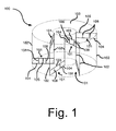
FIG. 1 is a schematic representation that is useful for understanding the structure of an improved toroidal inductor. -
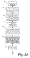
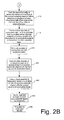
FIGS. 2A and2B illustrate a flow chart that is useful for understanding the method of making the present invention. -
FIG. 3 is a top view of a ceramic substrate layer with vias formed therein that is useful for understanding the invention. -
FIG. 4 is a cross-sectional view of the ceramic substrate layer ofFIG. 3 , taken along line 4-4. -
FIG. 5 is a top view of the ceramic substrate layer inFIG. 3 after the application of a pattern of conductive traces. -
FIG. 6 is a cross-sectional view of the ceramic substrate layer ofFIG. 5 , taken along line 6-6. -
FIG. 7 is a top view of a second ceramic substrate layer that is useful for understanding the invention. -
FIG. 8A is a cross-sectional view of the second ceramic substrate layer ofFIG. 7 , taken along theline 8A-8A. -
FIG. 8B is a partial expanded cross-sectional view of the second ceramic substrate layer ofFIG. 7 , taken along theline 8B-8B. -
FIG. 9 is a cross-sectional view showing the first ceramic substrate layer being positioned on top of the second ceramic substrate layer. -
FIG. 10 is a cross-sectional view of the first and second ceramic substrate layers in a stacked configuration that is useful for understanding the invention. -
FIG. 11 is a top view of a third ceramic substrate layer that is useful for understanding the invention. -
FIG. 12 is a cross-sectional view of the third ceramic substrate layer ofFIG. 11 , taken along the line 12-12. -
FIG. 13 is a cross-sectional view showing the third ceramic substrate layer being positioned on top of the first and second ceramic substrate layers. -
FIG. 14 is a cross-sectional view of the first, second and third ceramic substrate layers in a stacked configuration that is useful for understanding the invention. -
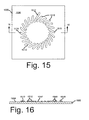
FIG. 15 is a top view of a fourth ceramic substrate layer that is useful for understanding the invention. -
FIG. 16 is a cross-sectional view of the fourth ceramic substrate layer ofFIG. 15 , taken along the line 16-16. -
FIG. 17 is a cross-sectional view showing the fourth substrate layer being positioned underneath the first, second, and third ceramic substrate layers. -
FIG. 18 is a cross-sectional view of the first, second, third, and fourth ceramic substrate layers in a stacked configuration that is useful for understanding the invention. -
FIG. 19 is a cross-sectional view of a second alternative embodiment of the toroidal inductor shown inFIG. 18 . - The invention concerns an improved toroidal inductor integrated within a ceramic substrate and a method of making same. For convenience, the substrate is described herein as a ceramic substrate. However, it should be understood that the invention is not limited in this regard. Substrates formed of other materials can also be used. For example, such materials include, but are not limited to liquid crystal polymer (LCP), polymer film, polyimide film, epoxy laminates, or semiconductor materials such as silicon, gallium arsenide, gallium nitride, germanium or indium phosphide.
- Referring to
FIG. 1 , a schematic representation of the improvedtoroidal inductor 100 is shown. Theinductor 100 comprises a coil formed of an elongated conductor defining a plurality of turns and extending around acore material 103. The improved toroidal coil structure includes a plurality of coil segments arranged in an alternating pattern. The coil segments include a firsttype coil segment 101 and a secondtype coil segment 102. The firsttype coil segment 101 is comprised of a plurality of elongatedparallel conductors parallel conductor 104 forms a first parallel conductor pair with a second elongatedparallel conductor 105. Theparallel conductors conductive link 108. The secondtype coil segments 102 provide a series electrical connection between spaced apart ones of the firsttype coil segment 101. - In a conventional embedded toroidal inductor, a first
type coil segment 101 is formed of a single conductive trace disposed on a surface of a substrate. However, such conductive traces have a relatively low cross sectional area. Accordingly, they tend to have a relatively high resistance. In the present invention, this problem is overcome by using a plurality of elongatedparallel conductors type coil segment 101. In the present invention,conductive links 108 are used to minimize the effect of any capacitance that might otherwise exist as between the elongatedparallel conductors type coil segments 102 can be formed as conductor filled vias using conventional circuit board manufacturing techniques. - A method for manufacturing a toroidal inductor having the form shown in
FIG. 1 shall now be described in the flowchart inFIGS. 2A and2B and with reference toFIGS. 1 and3-19 . Referring now toFIGS. 3 and 4 , the method can begin withstep 202 by forming a suitably sized piece of an unfiredceramic substrate layer 300. Theceramic substrate layer 300 can be any of a variety of commercially available glass ceramic substrates designed to be calcined at 800°C to 1,050°C. This class of materials is commonly referred to as low-temperature co-fired ceramics (LTCC). Such LTCC materials have a number of advantages that make them especially useful as substrates for RF systems. For example, low temperature 951 co-fire Green TapeTM from Dupont® is Au and Ag compatible, and it has a thermal coefficient of expansion (TCE) and relative strength that are suitable for many applications. Other similar types of ceramic tapes can also be used. The size of the ceramic tape can be determined by a variety of factors depending upon the particular application. For example, if the toroidal inductor is to form part of a larger RF circuit, the ceramic tape can be sized to accommodate the RF circuit in which the toroidal inductor forms a component. - A first plurality of
conductive vias 302 and a via 312 can be formed in the unfiredceramic substrate layer 300. This step can be performed using conventional techniques. For example, vias can be formed by punching, laser cutting, or etching holes in the unfiredceramic substrate layer 300. As shown inFIGS. 3 and 4 , the first plurality ofconductive vias 302 can be radially spaced a first distance d1 from acentral axis 401 so as to define an inner circumference of a toroidal inductor. Instep 206, a second plurality ofconductive vias 304 can be similarly formed radially spaced a second distance d2 about thecentral axis 401 so as to define an outer circumference. As shown inFIG. 4 , the vias can extend substantially between opposingsurfaces ceramic substrate layer 300. Each conductive via 302 can be positioned radially adjacent to a conductive via 304. - In general, the term "radially adjacent" means that two vias that are approximately radially aligned relative to
central axis 401 and positioned adjacent to each other.Vias FIG. 3 , circumferentially offset vias are not aligned radially. Instep 208, the via holes of the first and second pluralities ofconductive vias - Referring now to
FIGS. 5 and 6 , the process can continue instep 210 by disposing a first plurality ofconductive traces 510 onceramic substrate layer 300. The first plurality ofconductive traces 510 onsurface 306 form electrical connections between respective ones of the first plurality of conductive vias and second plurality of conductive vias that are substantially radially adjacent, as defined earlier. Moreover, additionalconductive traces - Referring now to
FIGS. 7, 8A, and 8B , the process continues by forming a secondceramic substrate layer 700. Instep 212, a third plurality ofconductive vias 803 are formed at predetermined intervals through the secondceramic substrate layer 700. The third plurality ofvias 803 is located within a predetermined area which corresponds to each of the respective lengths of second conductive traces 710 (discussed below). This concept is best understood by referring toFIG. 8B . As shown inFIG. 8B , eachtrace 710 has the third plurality ofvias 803 positioned at locations along the length of thetrace 710 and at opposing ends of thetrace 710. Instep 214, the third plurality ofconductive vias 803 are filled with conductive paste or any other suitable conductive element. Instep 216, a second plurality ofconductive traces 710 is provided onsurface 706 of thesecond substrate layer 700. Moreover, additionalconductive trace 717 can also be added to facilitate in the formation of electrical terminals. The second plurality ofconductive traces 710 is arranged so that when the first and second ceramic substrate layers 300, 700 are aligned and stacked as shown inFIGS. 9 and 10 , thetraces 710 onsurface 706 will provide an electrical connection between circumferentially offset ones of the first and second pluralities ofconductive vias - Referring now to
FIGS. 11 and 12 , the process continues by forming a thirdceramic substrate layer 1100. Instep 218, a fourth plurality ofconductive vias 1203 are formed at predetermined intervals through the thirdceramic substrate layer 1100. The hole locations are defined within the respective lengths of third conductive traces 1110 (discussed below). Instep 220, the fourth plurality ofconductive vias 1203 are filled with conductive paste or any other suitable conductive element. Instep 222, the third plurality ofconductive traces 1110 is provided onsurface 1106 of thethird substrate layer 1100. Moreover, additionalconductive traces - The third plurality of
conductive traces 1110 is arranged so that when the ceramic substrate layers 300 and 1100 are aligned and stacked as shown inFIGS. 13 and 14 , thetraces 1110 onsurface 1106 and the conductive traces 510 onsurface 306 define a plurality of elongated parallel conductors. The elongated parallel conductors are aligned with each other, spaced apart and electrically connected by conductive links defined by the fourth plurality ofconductive vias 1203. - Referring now to
FIGS. 15 and 16 , the process continues by forming a fourthceramic substrate layer 1500. Instep 224, a fourth plurality ofconductive traces 1510 is provided onsurface 1506 of thefourth substrate layer 1500. The fourth plurality ofconductive traces 1510 are arranged in the same manner as the second plurality of conductive traces 710. Moreover, additionalconductive trace 1517 can also be added to facilitate in the formation of electrical terminals. - The fourth plurality of
conductive traces 1510 is arranged so that when the ceramic substrate layers 700 and 1500 are aligned and stacked as shown inFIGS. 17 and 18 , thetraces 710 onsurface 706 and theconductive traces 1510 onsurface 1506 define a plurality of elongated parallel conductors. The elongated parallel conductors are aligned with each other, spaced apart, and electrically connected by conductive links defined by the fourth plurality ofconductive vias 1203. The combination of elongated parallel conductors and conductive links serves to lower the direct current resistance in the system by increasing the effective cross-sectional area of the traces, hence improving the quality factor (Q) of the inductor. For example, in testing using standard DCR measuring instruments, the improved toroidal inductor design had a lower DCR value as compared to conventional toroidal inductors. Specifically, the DCR value was reduced by nearly one-half. - The conductive traces 510, 710, 1110, and 1510 can be formed of any suitable conductive film, paste, or ink that is compatible with the co-firing process for the selected LTCC material. Such materials are commercially available from a variety of sources. Further, it should be noted that for purposes of consistency with standard LTCC processing, each of the ceramic substrate layers shown in
FIGS. 6 ,8A ,12 , and16 contain conductive traces disposed on one side of each ceramic substrate layer only. However, the invention is not so limited. Those skilled in the art will appreciate that it is possible for the conductive traces to instead be disposed on opposing sides of a single layer of ceramic tape. Such alternative arrangements are intended to be within the scope of the invention. For example, such an alternative arrangement is shown inFIG. 19 , where structure common toFIG. 18 is identified using like reference numerals.FIG. 19 shows secondceramic substrate layer 700, which includesconductive traces step 226, thevarious LTCC layers - In their stacked configuration shown in
FIG. 18 , theconductive vias conductive traces FIG. 18 together define a three dimensional conductivetoroidal coil 100, which is best illustrated by the schematic representation inFIG. 1 . In particular,FIG. 1 is useful for understanding the toroidal coil structure of the inventive arrangements. In this regard, it should be understood that the invention herein is not limited to the precise arrangement or pattern ofvias FIG. 18 . Instead, any pattern, geometry, and number of vias and traces formed in the ceramic substrate layer can be used provided that it generally results in a substantially toroidal coil arrangement of the kind similar to that illustrated inFIG. 1 - In
FIGS. 1 and3-19 there is shown a toroidal coil in which the parallel conductive traces are comprised of only two elongatedparallel conductors - Referring back to
FIGS. 3 ,5 ,7 , and11 , the combination of additionalconductive vias 312 and additionalconductive traces step 228 in accordance with a temperature and time appropriate for the particular type of ceramic tape to sinter and densify.
Claims (17)
- An inductor, comprising:a coil formed from an elongated conductor extending around a core material and defining a plurality of turns;said elongated conductor comprised of at least one coil segment of a first type, each said coil segment of said first type comprised of a plurality of elongated parallel conductors spaced apart and electrically connected by conductive links at predetermined intervals along their respective lengths.
- The inductor according to claim 1, wherein said elongated conductor is further comprised of at least one coil segment of a second type, said coil segment of said second type formed of a single conductor.
- The inductor according to claim 2, wherein said coil segment of said first type and said coil segment of said second type are arranged in a series configuration to form said elongated conductor.
- The inductor according to claim 3, wherein said elongated conductor is comprised of a plurality of said coil segments of said first type and a plurality of said coil segments of said second type, each said coil segment of said second type defining a series electrical connection between coil segments of said first type.
- The inductor according to claim 2, wherein each said single conductor comprising said coil segment of said second type is comprised of a conductive via formed in a substrate.
- The inductor according to claim 1, wherein each of said elongated parallel conductors is comprised of a conductive trace disposed on a surface of a substrate.
- The inductor according to claim 1 wherein said conductive links are formed from vias defined in a substrate.
- An inductor, comprising:a coil formed from an elongated conductor extending around a core material and defining a plurality of turns;said elongated conductor comprised of a plurality of coil segments arranged in an alternating pattern of a first type segment and a second type segment, said first type segment comprising a plurality of parallel conductors spaced apart and electrically connected at predetermined intervals along a length of said plurality of parallel conductors and said second type segment comprising a single elongated conductor.
- The inductor according to claim 8, wherein said second type segments are comprised of conductive vias formed in a substrate.
- The inductor according to claim 8, wherein each said parallel conductor is comprised of a conductive trace disposed on a surface of a substrate, and said conductive traces are connected at said predetermined intervals by at least one conductive via.
- A method for forming an inductor, comprising:forming a coil from an elongated conductor extending around a core material to define a plurality of turns;forming said elongated conductor to include at least one coil segment of a first type comprised of a plurality of elongated parallel conductors spaced apart; andelectrically connecting said elongated parallel conductors by means of conductive links spaced at predetermined intervals along a length of said plurality of elongated parallel conductors.
- The method according to claim 11, further comprising forming said elongated conductor of at least one coil segment of a second type, said coil segment of said second type formed of a single conductor.
- The method according to claim 12, further comprising arranging said at least one coil segment of said first type and said at least one coil segment of said second type in a series configuration to form said elongated conductor.
- The method according to claim 13, further comprising forming with said at least one coil segment of said second type a series electrical connection between a plurality of said coil segments of said first type.
- The method according to claim 12, further comprising forming each said coil segment of said second type as a conductive via formed in a substrate.
- The method according to claim 11, further comprising forming each of said parallel conductors as a conductive trace disposed on a surface of a substrate.
- The method according to claim 11 further comprising forming said conductive links from vias defined in a substrate.
Applications Claiming Priority (1)
| Application Number | Priority Date | Filing Date | Title |
|---|---|---|---|
| US11/624,321 US7304558B1 (en) | 2007-01-18 | 2007-01-18 | Toroidal inductor design for improved Q |
Publications (1)
| Publication Number | Publication Date |
|---|---|
| EP1947658A1 true EP1947658A1 (en) | 2008-07-23 |
Family
ID=38775442
Family Applications (1)
| Application Number | Title | Priority Date | Filing Date |
|---|---|---|---|
| EP08000854A Withdrawn EP1947658A1 (en) | 2007-01-18 | 2008-01-17 | Toroidal inductor design for improved Q |
Country Status (4)
| Country | Link |
|---|---|
| US (1) | US7304558B1 (en) |
| EP (1) | EP1947658A1 (en) |
| JP (1) | JP2008177574A (en) |
| CA (1) | CA2618688C (en) |
Cited By (1)
| Publication number | Priority date | Publication date | Assignee | Title |
|---|---|---|---|---|
| DE102008062870A1 (en) * | 2008-12-17 | 2010-07-01 | Würth Elektronik eiSos Gmbh & Co. KG | Inductance component for use on printed circuit board for producing coil surrounding coil cores, has u-shaped conductor sections arranged in housing, and brackets whose ends are connectably formed for formation of coil surrounding core |
Families Citing this family (15)
| Publication number | Priority date | Publication date | Assignee | Title |
|---|---|---|---|---|
| US7436282B2 (en) * | 2004-12-07 | 2008-10-14 | Multi-Fineline Electronix, Inc. | Miniature circuitry and inductive components and methods for manufacturing same |
| TWI416557B (en) * | 2004-12-07 | 2013-11-21 | Multi Fineline Electronix Inc | Micro-transformer, multilayer printed wiring, wiring, and method for forming plated through holes and insulated conductor vias |
| DE102006025194A1 (en) * | 2006-05-29 | 2007-12-06 | Endress + Hauser Conducta Gesellschaft für Mess- und Regeltechnik mbH + Co. KG | Inductive conductivity sensor for measuring electrical conductivity of medium, has toroidal coils, which enclose continuous opening that is subjected to medium, and several conductor sections, which are connected by through connections |
| US7524731B2 (en) * | 2006-09-29 | 2009-04-28 | Freescale Semiconductor, Inc. | Process of forming an electronic device including an inductor |
| WO2008152641A2 (en) * | 2007-06-12 | 2008-12-18 | Advanced Magnetic Solutions Ltd. | Magnetic induction devices and methods for producing them |
| JP5902440B2 (en) * | 2011-10-31 | 2016-04-13 | 京セラ株式会社 | Inductor parts and electronic devices |
| US9431473B2 (en) | 2012-11-21 | 2016-08-30 | Qualcomm Incorporated | Hybrid transformer structure on semiconductor devices |
| US10002700B2 (en) | 2013-02-27 | 2018-06-19 | Qualcomm Incorporated | Vertical-coupling transformer with an air-gap structure |
| US9634645B2 (en) | 2013-03-14 | 2017-04-25 | Qualcomm Incorporated | Integration of a replica circuit and a transformer above a dielectric substrate |
| US9449753B2 (en) | 2013-08-30 | 2016-09-20 | Qualcomm Incorporated | Varying thickness inductor |
| US9906318B2 (en) | 2014-04-18 | 2018-02-27 | Qualcomm Incorporated | Frequency multiplexer |
| CN207098945U (en) | 2014-11-12 | 2018-03-13 | 株式会社村田制作所 | Power module and its installation structure |
| WO2016147845A1 (en) * | 2015-03-16 | 2016-09-22 | 株式会社村田製作所 | Inductor component |
| US9947456B2 (en) | 2015-11-24 | 2018-04-17 | The University Of North Carolina At Charlotte | High power density printed circuit board (PCB) embedded inductors |
| JP6838548B2 (en) * | 2017-12-07 | 2021-03-03 | 株式会社村田製作所 | Coil parts and their manufacturing methods |
Citations (1)
| Publication number | Priority date | Publication date | Assignee | Title |
|---|---|---|---|---|
| US20030112114A1 (en) | 2001-12-13 | 2003-06-19 | International Business Machines Corporation | Embedded inductor and method of making |
Family Cites Families (16)
| Publication number | Priority date | Publication date | Assignee | Title |
|---|---|---|---|---|
| JPS63272020A (en) * | 1987-04-30 | 1988-11-09 | Harada Kogyo Kk | Toroidal coil device and manufacture thereof |
| US5055816A (en) * | 1989-06-26 | 1991-10-08 | Motorola, Inc. | Method for fabricating an electronic device |
| DE4027994A1 (en) * | 1990-09-04 | 1992-03-05 | Gw Elektronik Gmbh | HF MAGNETIC COIL ARRANGEMENT AND METHOD FOR THEIR PRODUCTION |
| US5781091A (en) * | 1995-07-24 | 1998-07-14 | Autosplice Systems Inc. | Electronic inductive device and method for manufacturing |
| JP4030028B2 (en) * | 1996-12-26 | 2008-01-09 | シチズン電子株式会社 | SMD type circuit device and manufacturing method thereof |
| US6054914A (en) | 1998-07-06 | 2000-04-25 | Midcom, Inc. | Multi-layer transformer having electrical connection in a magnetic core |
| US6198374B1 (en) | 1999-04-01 | 2001-03-06 | Midcom, Inc. | Multi-layer transformer apparatus and method |
| US6820321B2 (en) * | 2000-09-22 | 2004-11-23 | M-Flex Multi-Fineline Electronix, Inc. | Method of making electronic transformer/inductor devices |
| JP2002289436A (en) * | 2001-03-28 | 2002-10-04 | Niigata Seimitsu Kk | Inductance element |
| JP2004006458A (en) * | 2002-05-31 | 2004-01-08 | Canon Inc | coil |
| WO2004112138A1 (en) * | 2003-06-16 | 2004-12-23 | Nec Corporation | Semiconductor device and method for manufacturing same |
| US6990729B2 (en) | 2003-09-05 | 2006-01-31 | Harris Corporation | Method for forming an inductor |
| JP2005259878A (en) * | 2004-03-10 | 2005-09-22 | Murata Mfg Co Ltd | Laminated coil component |
| US7196607B2 (en) * | 2004-03-26 | 2007-03-27 | Harris Corporation | Embedded toroidal transformers in ceramic substrates |
| JP4682606B2 (en) * | 2004-12-07 | 2011-05-11 | ソニー株式会社 | Inductance element, manufacturing method thereof, and wiring board |
| JP2006173145A (en) * | 2004-12-10 | 2006-06-29 | Sharp Corp | Inductors, resonant circuits, semiconductor integrated circuits, oscillators, communication devices |
-
2007
- 2007-01-18 US US11/624,321 patent/US7304558B1/en active Active
-
2008
- 2008-01-16 CA CA2618688A patent/CA2618688C/en not_active Expired - Fee Related
- 2008-01-17 EP EP08000854A patent/EP1947658A1/en not_active Withdrawn
- 2008-01-17 JP JP2008007778A patent/JP2008177574A/en active Pending
Patent Citations (1)
| Publication number | Priority date | Publication date | Assignee | Title |
|---|---|---|---|---|
| US20030112114A1 (en) | 2001-12-13 | 2003-06-19 | International Business Machines Corporation | Embedded inductor and method of making |
Cited By (1)
| Publication number | Priority date | Publication date | Assignee | Title |
|---|---|---|---|---|
| DE102008062870A1 (en) * | 2008-12-17 | 2010-07-01 | Würth Elektronik eiSos Gmbh & Co. KG | Inductance component for use on printed circuit board for producing coil surrounding coil cores, has u-shaped conductor sections arranged in housing, and brackets whose ends are connectably formed for formation of coil surrounding core |
Also Published As
| Publication number | Publication date |
|---|---|
| CA2618688C (en) | 2012-03-13 |
| JP2008177574A (en) | 2008-07-31 |
| US7304558B1 (en) | 2007-12-04 |
| CA2618688A1 (en) | 2008-07-18 |
Similar Documents
| Publication | Publication Date | Title |
|---|---|---|
| CA2618688C (en) | Toroidal inductor design for improved q | |
| TWI321327B (en) | Embedded toroidal inductor | |
| US7513031B2 (en) | Method for forming an inductor in a ceramic substrate | |
| CN1938794B (en) | Embedded toroidal transformers in ceramic substrates | |
| US7449987B2 (en) | Transformer and associated method of making | |
| US20140218883A1 (en) | Electronic module allowing fine tuning after assembly | |
| KR101215303B1 (en) | Electronic device comprising ltcc inductor | |
| KR101057567B1 (en) | Related Manufacturing Methods Using Transformers and Liquid Crystal Polymer (LCP) Materials | |
| CN109511213A (en) | Circuit board and flat surface transformer | |
| US20140334120A1 (en) | Electronic module allowing fine tuning after assembly | |
| JP2000188475A (en) | Manufacture of ceramic multilayer substrate | |
| JP2005136878A (en) | High frequency filter |
Legal Events
| Date | Code | Title | Description |
|---|---|---|---|
| PUAI | Public reference made under article 153(3) epc to a published international application that has entered the european phase |
Free format text: ORIGINAL CODE: 0009012 |
|
| 17P | Request for examination filed |
Effective date: 20080117 |
|
| AK | Designated contracting states |
Kind code of ref document: A1 Designated state(s): AT BE BG CH CY CZ DE DK EE ES FI FR GB GR HR HU IE IS IT LI LT LU LV MC MT NL NO PL PT RO SE SI SK TR |
|
| AX | Request for extension of the european patent |
Extension state: AL BA MK RS |
|
| AKX | Designation fees paid |
Designated state(s): DE FR GB |
|
| STAA | Information on the status of an ep patent application or granted ep patent |
Free format text: STATUS: THE APPLICATION HAS BEEN WITHDRAWN |
|
| 18W | Application withdrawn |
Effective date: 20121019 |